US10027916B2 - Solid-state imaging device and electronic apparatus - Google Patents
Solid-state imaging device and electronic apparatus Download PDFInfo
- Publication number
- US10027916B2 US10027916B2 US15/314,976 US201515314976A US10027916B2 US 10027916 B2 US10027916 B2 US 10027916B2 US 201515314976 A US201515314976 A US 201515314976A US 10027916 B2 US10027916 B2 US 10027916B2
- Authority
- US
- United States
- Prior art keywords
- amplification transistors
- transistor
- resistance
- amplification
- selection transistor
- Prior art date
- Legal status (The legal status is an assumption and is not a legal conclusion. Google has not performed a legal analysis and makes no representation as to the accuracy of the status listed.)
- Active
Links
- 238000003384 imaging method Methods 0.000 title claims abstract description 56
- 230000003321 amplification Effects 0.000 claims abstract description 175
- 238000003199 nucleic acid amplification method Methods 0.000 claims abstract description 175
- 238000006243 chemical reaction Methods 0.000 claims abstract description 21
- 238000009792 diffusion process Methods 0.000 claims abstract description 21
- 238000000926 separation method Methods 0.000 claims description 7
- 238000005516 engineering process Methods 0.000 abstract description 23
- 230000002542 deteriorative effect Effects 0.000 abstract description 8
- 238000010586 diagram Methods 0.000 description 17
- 230000000875 corresponding effect Effects 0.000 description 15
- 230000003247 decreasing effect Effects 0.000 description 14
- 239000000758 substrate Substances 0.000 description 8
- 239000004065 semiconductor Substances 0.000 description 7
- 230000006866 deterioration Effects 0.000 description 3
- 229920006395 saturated elastomer Polymers 0.000 description 3
- 230000000295 complement effect Effects 0.000 description 2
- 230000006870 function Effects 0.000 description 2
- 239000011159 matrix material Substances 0.000 description 2
- 229910044991 metal oxide Inorganic materials 0.000 description 2
- 150000004706 metal oxides Chemical class 0.000 description 2
- 230000003287 optical effect Effects 0.000 description 2
- 230000002093 peripheral effect Effects 0.000 description 2
- 230000035945 sensitivity Effects 0.000 description 2
- 230000015572 biosynthetic process Effects 0.000 description 1
- 230000002596 correlated effect Effects 0.000 description 1
- 230000000694 effects Effects 0.000 description 1
- 238000005468 ion implantation Methods 0.000 description 1
- 230000004048 modification Effects 0.000 description 1
- 238000012986 modification Methods 0.000 description 1
- 238000005070 sampling Methods 0.000 description 1
- 230000000087 stabilizing effect Effects 0.000 description 1
Images


Classifications
-
- H04N5/37457—
-
- H—ELECTRICITY
- H04—ELECTRIC COMMUNICATION TECHNIQUE
- H04N—PICTORIAL COMMUNICATION, e.g. TELEVISION
- H04N25/00—Circuitry of solid-state image sensors [SSIS]; Control thereof
- H04N25/70—SSIS architectures; Circuits associated therewith
- H04N25/76—Addressed sensors, e.g. MOS or CMOS sensors
- H04N25/77—Pixel circuitry, e.g. memories, A/D converters, pixel amplifiers, shared circuits or shared components
- H04N25/778—Pixel circuitry, e.g. memories, A/D converters, pixel amplifiers, shared circuits or shared components comprising amplifiers shared between a plurality of pixels, i.e. at least one part of the amplifier must be on the sensor array itself
-
- H—ELECTRICITY
- H01—ELECTRIC ELEMENTS
- H01L—SEMICONDUCTOR DEVICES NOT COVERED BY CLASS H10
- H01L27/00—Devices consisting of a plurality of semiconductor or other solid-state components formed in or on a common substrate
- H01L27/14—Devices consisting of a plurality of semiconductor or other solid-state components formed in or on a common substrate including semiconductor components sensitive to infrared radiation, light, electromagnetic radiation of shorter wavelength or corpuscular radiation and specially adapted either for the conversion of the energy of such radiation into electrical energy or for the control of electrical energy by such radiation
- H01L27/144—Devices controlled by radiation
- H01L27/146—Imager structures
- H01L27/14601—Structural or functional details thereof
- H01L27/14603—Special geometry or disposition of pixel-elements, address-lines or gate-electrodes
-
- H—ELECTRICITY
- H01—ELECTRIC ELEMENTS
- H01L—SEMICONDUCTOR DEVICES NOT COVERED BY CLASS H10
- H01L27/00—Devices consisting of a plurality of semiconductor or other solid-state components formed in or on a common substrate
- H01L27/14—Devices consisting of a plurality of semiconductor or other solid-state components formed in or on a common substrate including semiconductor components sensitive to infrared radiation, light, electromagnetic radiation of shorter wavelength or corpuscular radiation and specially adapted either for the conversion of the energy of such radiation into electrical energy or for the control of electrical energy by such radiation
- H01L27/144—Devices controlled by radiation
- H01L27/146—Imager structures
- H01L27/14601—Structural or functional details thereof
- H01L27/14609—Pixel-elements with integrated switching, control, storage or amplification elements
- H01L27/14612—Pixel-elements with integrated switching, control, storage or amplification elements involving a transistor
- H01L27/14614—Pixel-elements with integrated switching, control, storage or amplification elements involving a transistor having a special gate structure
-
- H—ELECTRICITY
- H01—ELECTRIC ELEMENTS
- H01L—SEMICONDUCTOR DEVICES NOT COVERED BY CLASS H10
- H01L27/00—Devices consisting of a plurality of semiconductor or other solid-state components formed in or on a common substrate
- H01L27/14—Devices consisting of a plurality of semiconductor or other solid-state components formed in or on a common substrate including semiconductor components sensitive to infrared radiation, light, electromagnetic radiation of shorter wavelength or corpuscular radiation and specially adapted either for the conversion of the energy of such radiation into electrical energy or for the control of electrical energy by such radiation
- H01L27/144—Devices controlled by radiation
- H01L27/146—Imager structures
- H01L27/14601—Structural or functional details thereof
- H01L27/14641—Electronic components shared by two or more pixel-elements, e.g. one amplifier shared by two pixel elements
-
- H—ELECTRICITY
- H01—ELECTRIC ELEMENTS
- H01L—SEMICONDUCTOR DEVICES NOT COVERED BY CLASS H10
- H01L27/00—Devices consisting of a plurality of semiconductor or other solid-state components formed in or on a common substrate
- H01L27/14—Devices consisting of a plurality of semiconductor or other solid-state components formed in or on a common substrate including semiconductor components sensitive to infrared radiation, light, electromagnetic radiation of shorter wavelength or corpuscular radiation and specially adapted either for the conversion of the energy of such radiation into electrical energy or for the control of electrical energy by such radiation
- H01L27/144—Devices controlled by radiation
- H01L27/146—Imager structures
- H01L27/14643—Photodiode arrays; MOS imagers
-
- H—ELECTRICITY
- H04—ELECTRIC COMMUNICATION TECHNIQUE
- H04N—PICTORIAL COMMUNICATION, e.g. TELEVISION
- H04N25/00—Circuitry of solid-state image sensors [SSIS]; Control thereof
- H04N25/60—Noise processing, e.g. detecting, correcting, reducing or removing noise
-
- H—ELECTRICITY
- H04—ELECTRIC COMMUNICATION TECHNIQUE
- H04N—PICTORIAL COMMUNICATION, e.g. TELEVISION
- H04N25/00—Circuitry of solid-state image sensors [SSIS]; Control thereof
- H04N25/60—Noise processing, e.g. detecting, correcting, reducing or removing noise
- H04N25/616—Noise processing, e.g. detecting, correcting, reducing or removing noise involving a correlated sampling function, e.g. correlated double sampling [CDS] or triple sampling
-
- H—ELECTRICITY
- H04—ELECTRIC COMMUNICATION TECHNIQUE
- H04N—PICTORIAL COMMUNICATION, e.g. TELEVISION
- H04N25/00—Circuitry of solid-state image sensors [SSIS]; Control thereof
- H04N25/60—Noise processing, e.g. detecting, correcting, reducing or removing noise
- H04N25/618—Noise processing, e.g. detecting, correcting, reducing or removing noise for random or high-frequency noise
-
- H—ELECTRICITY
- H04—ELECTRIC COMMUNICATION TECHNIQUE
- H04N—PICTORIAL COMMUNICATION, e.g. TELEVISION
- H04N25/00—Circuitry of solid-state image sensors [SSIS]; Control thereof
- H04N25/60—Noise processing, e.g. detecting, correcting, reducing or removing noise
- H04N25/67—Noise processing, e.g. detecting, correcting, reducing or removing noise applied to fixed-pattern noise, e.g. non-uniformity of response
- H04N25/671—Noise processing, e.g. detecting, correcting, reducing or removing noise applied to fixed-pattern noise, e.g. non-uniformity of response for non-uniformity detection or correction
- H04N25/677—Noise processing, e.g. detecting, correcting, reducing or removing noise applied to fixed-pattern noise, e.g. non-uniformity of response for non-uniformity detection or correction for reducing the column or line fixed pattern noise
-
- H—ELECTRICITY
- H04—ELECTRIC COMMUNICATION TECHNIQUE
- H04N—PICTORIAL COMMUNICATION, e.g. TELEVISION
- H04N25/00—Circuitry of solid-state image sensors [SSIS]; Control thereof
- H04N25/70—SSIS architectures; Circuits associated therewith
- H04N25/76—Addressed sensors, e.g. MOS or CMOS sensors
- H04N25/77—Pixel circuitry, e.g. memories, A/D converters, pixel amplifiers, shared circuits or shared components
-
- H04N5/357—
Definitions
- the present technology relates to a solid-state imaging device and an electronic apparatus, in particularly to a solid-state imaging device and electronic apparatus that realize a high frame rate image capture.
- a layout of transistors may cause a variation of sensitivity among a plurality of photodiodes within a shared pixel.
- a high frame rate image capture is performed by a digital video camera in the related art in order to acquire a slow motion video, and capture an object to be imaged that moves quickly in sports broadcasting or the like.
- CMOS Complementary Metal Oxide Semiconductor
- transconductance gm of the amplification transistor may be increased.
- a gate length L of the amplification transistor may be decreased or a gate width W thereof may be increased.
- Patent Document 1 Japanese Patent Application Laid-open No. 2013-62789
- the gate length L of the amplification transistor is decreased, or the gate width W thereof is increased, a random noise of the amplification transistor may be increased or a saturated signal amount of a pixel may be decreased, which may result in a deteriorated image quality.
- the present technology is made in view of the circumstances as described above to realize a high frame rate image capture without deteriorating an image quality.
- a solid-state imaging device includes one or more photoelectric conversion units; a floating diffusion that holds a charge accumulated on the photoelectric conversion units; a plurality of amplification transistors that read out a signal corresponding to the charge held by the floating diffusion; and a vertical signal line to which the signal read out by the amplification transistor is output, and the plurality of amplification transistors are connected in parallel.
- a selection transistor that outputs the signal read out by the plurality of amplification transistors to the vertical signal line may be further included.
- the number of the selection transistor may be the same or less as the number of the plurality of amplification transistors.
- the plurality of amplification transistors may be connected to the vertical signal line via the selection transistor.
- the plurality of amplification transistors may be formed on an identical active region.
- the plurality of amplification transistors may be formed on different active regions, and an element separation region may be formed between the different active regions.
- a threshold voltage of the selection transistor may be set lower than a threshold voltage of the plurality of amplification transistors.
- a load transistor connected to the vertical signal line may by further included.
- On-resistance of the load transistor may be set smaller than a sum of on-resistance of the plurality of amplification transistors and on-resistance of the selection transistor.
- the on-resistance of the load transistor may be set smaller than the sum of the on-resistance of the plurality of amplification transistors and the on-resistance of the selection transistor by setting the threshold voltage of the load transistor lower.
- the on-resistance of the load transistor may be set smaller than the sum of the on-resistance of the plurality of amplification transistors and the on-resistance of the selection transistor by setting the threshold voltage of the load transistor higher.
- the on-resistance of the load transistor may be set smaller than the sum of the on-resistance of the plurality of amplification transistors and the on-resistance of the selection transistor by setting a load current value of the load transistor smaller.
- An electronic apparatus includes a solid-state imaging device, including one or more photoelectric conversion units, a floating diffusion that holds a charge accumulated on the photoelectric conversion units, a plurality of amplification transistors that read out a signal corresponding to the charge held by the floating diffusion, and a vertical signal line to which the signal read out by the amplification transistor is output, the plurality of amplification transistors being connected in parallel.
- a solid-state imaging device including one or more photoelectric conversion units, a floating diffusion that holds a charge accumulated on the photoelectric conversion units, a plurality of amplification transistors that read out a signal corresponding to the charge held by the floating diffusion, and a vertical signal line to which the signal read out by the amplification transistor is output, the plurality of amplification transistors are connected in parallel.
- FIGS. 1A, 1B, 1C are views for explaining problems of a solid-state imaging device in the related art.
- FIG. 2 is a block diagram of a solid-state imaging device to which the present technology is applied.
- FIG. 3 is a circuit diagram showing a configuration example of a pixel of the solid-state imaging device.
- FIGS. 4A, 4B are plan views showing a layout example of a pixel of the solid-state imaging device.
- FIG. 5 is a circuit diagram showing a configuration example of a pixel of the solid-state imaging device.
- FIGS. 6A, 6B are plan views showing a layout example of a pixel of the solid-state imaging device.
- FIG. 7 is a circuit diagram showing a configuration example of a pixel sharing type pixel.
- FIGS. 8A, 8B are plan views showing a layout example of a pixel sharing type pixel.
- FIG. 9 is a circuit diagram showing a configuration example of a pixel sharing type pixel.
- FIG. 10A, 10B are plan views showing a configuration example of a pixel sharing type pixel.
- FIG. 11 is a circuit diagram showing a part of a pixel configuration in the related art.
- FIG. 12 is a circuit diagram showing a part of a pixel configuration to which the present technology is applied.
- FIG. 13 is a view for explaining linearity deterioration of a gain of a selection transistor.
- FIGS. 14A, 14B, 14C are views for explaining on-resistance variation of a load MOS transistor.
- FIGS. 15A, 15B are views showing a specific example of decreasing on-resistance of the load MOS transistor.
- FIGS. 16A, 16B are views showing a specific example of decreasing on-resistance of the load MOS transistor.
- FIGS. 17A, 17B are views showing a specific example of decreasing on-resistance of the load MOS transistor.
- FIG. 18 is a block diagram showing a configuration example of an electronic apparatus to which the present technology is applied.
- FIGS. 1A, 1B, 1C are plan views showing a layout example of a pixel of a solid-state imaging device in the related art.
- FIG. 1A shows four pixels 11 , each pixel 11 shares four pixels of vertical two pixels and horizontal two pixels.
- Each pixel 11 includes a photodiode (PD) 21 as a photoelectric conversion unit, transfer transistor 22 , a floating diffusion (FD) 23 , a reset transistor 24 , an amplification transistor 25 , and a selection transistor 26 .
- PD photodiode
- FD 23 floating diffusion
- reset transistor 24 reset transistor
- amplification transistor 25 amplification transistor
- selection transistor 26 selection transistor
- transconductance gm of an amplification transistor may be increased. It is also known that the transconductance gm is increased by decreasing a gate length L of the amplification transistor or increasing a gate width W thereof.
- a random noise of the amplification transistor is inversely proportional to a product of the gate length L and the gate width W of the amplification transistor. Accordingly, as shown FIG. 1B , when the gate length L of the amplification transistor 25 is decreased, the random noise of the amplification transistor 25 is increased.
- the gate length L of the amplification transistor is decreased or the gate width W thereof is increased, which may deteriorate an image quality.
- FIG. 2 is a block diagram showing an embodiment of a solid-state imaging device to which the present technology is applied.
- CMOS Complementary Metal Oxide Semiconductor
- FIG. 2 is a block diagram showing an embodiment of a solid-state imaging device to which the present technology is applied.
- CMOS Complementary Metal Oxide Semiconductor
- FIG. 2 is a block diagram showing an embodiment of a solid-state imaging device to which the present technology is applied.
- CMOS Complementary Metal Oxide Semiconductor
- the present technology is not limited to be applied to the surface irradiation type CMOS image sensor, and is also applicable to a rear surface irradiation type CMOS image sensor, other amplifying type solid-state imaging device, or a charge transfer type solid-state imaging device such as a CCD (Charge Coupled Device) image sensor.
- CCD Charge Coupled Device
- a CMOS image sensor 50 shown in FIG. 2 has a configuration that includes a pixel array unit 51 formed on a semiconductor substrate (not shown), and a peripheral circuit unit accumulated on the same semiconductor substrate of the pixel array unit 51 .
- the peripheral circuit unit is configured of a vertical driving unit 52 , a column processing unit 53 , a horizontal driving unit 54 , and a system control unit 55 , for example.
- the CMOS image sensor 50 includes a signal processing unit 58 and a data storing unit 59 .
- the pixel array unit 51 has a configuration that unit pixels (hereinafter referred to simply as “pixels”) are two-dimensionally arrayed in a row direction and a column direction, i.e., in a matrix.
- Each pixel includes a photoelectric conversion unit that generates and accumulates light charges corresponding to an amount of light received.
- the row direction represents an arrangement direction (horizontal direction) of the pixels in a pixel row
- the column direction represents an arrangement direction (vertical direction) of the pixels in a pixel column.
- pixel driving lines 56 are wired along the row direction for every pixel row, and vertical signal lines 57 are wired along the column direction for every pixel column to the pixel arrangement in the matrix.
- the pixel driving lines 56 transmit driving signals for driving when the signals are read-out from the pixels.
- the vertical driving unit 52 is configured of a shift resistor, an address decoder and the like, and drives all respective pixels of the pixel array unit 51 at the same time, in a row unit, or the like. In other words, the vertical driving unit 52 configures a driving unit for driving each pixel of the pixel array unit 51 together with the system control unit 55 that controls the vertical driving unit 52 .
- the signal output from each unit pixel in the pixel column selectively driven by the vertical driving unit 52 is input to the column processing unit 53 through each of the vertical signal lines 57 for every pixel column.
- the column processing unit 53 performs predetermined signal processing to the signal output from each pixel in a selection column through the vertical signal lines 57 for every pixel column of the pixel array unit 51 , and temporary holds a signal-processed pixel signal.
- the column processing unit 53 performs at least a noise removal processing, for example, CDS (Correlated Double Sampling) processing as the signal processing.
- CDS Correlated Double Sampling
- a fixed pattern noise characteristic to the pixel such as a reset noise, a threshold variation of the amplification transistor within the pixel or the like is removed.
- AD Analog-Digital
- the horizontal driving unit 54 is configured of a shift resistor, an address decoder and the like, and selects in turn a unit circuit corresponding to the pixel column of the column processing unit 53 . By the selective scanning of the horizontal driving unit 54 , a pixel signal processed for every unit circuit in the column processing unit 53 is output in turn.
- the system control unit 55 is configured of a timing generator that generates a variety of timing signals or the like, and performs a drive control of the vertical driving unit 52 , the column processing unit 53 , the horizontal driving unit 54 and the like on the basis of the variety of timing signals generated by the timing generator.
- the signal processing unit 58 has at least an arithmetic processing function, and performs various signal processing such as arithmetic processing on a pixel signal output from the column processing unit 53 .
- the data storing unit 59 temporary stores data needed for the signal processing at the signal processing unit 58 .
- the signal processing unit 58 and the data storing unit 59 may be mounted on the same substrate (semiconductor substrate) as the CMOS image sensor 50 , or may be disposed on a separate substrate from the CMOS image sensor 50 .
- each processing of the signal processing unit 58 and the data storing unit 59 may be performed as external signal processing unit disposed on a separate substrate from the CMOS image sensor 50 , e.g., processing by the DSP (Digital Signal Processor) circuit or software.
- DSP Digital Signal Processor
- CMOS image sensor 50 when the CMOS image sensor 50 is the rear surface irradiation type CMOS image sensor, it may be configured as a laminate type CMOS image sensor where a semiconductor substrate including the pixel array unit 51 is adhered to a semiconductor substrate including a logic circuit.
- FIG. 3 is a circuit diagram showing a configuration example of a pixel disposed on the pixel array unit 51 .
- the pixel 61 includes a photodiode (PD) 71 as a photoelectric conversion unit, a transfer transistor 72 , a floating diffusion (FD) 73 , a reset transistor 74 , amplification transistors 75 - 1 , 75 - 2 , and a selection transistor 76 .
- PD photodiode
- FD floating diffusion
- reset transistor 74 reset transistor
- amplification transistors 75 - 1 , 75 - 2 the pixel 61 includes a selection transistor 76 .
- any pixel transistor included in the pixel 61 is configured of an n type MOS transistor.
- An anode of the PD 71 is grounded, and a cathode of the PD 71 is connected to a source of the transfer transistor 72 .
- a drain of the transfer transistor 72 is connected to each gate of the amplification transistors 75 - 1 , 75 - 2 , and connection points configure the FD 73 .
- the reset transistor 74 is connected between a predetermined power source Vdd and the FD 73 .
- Each drain of the amplification transistors 75 - 1 , 75 - 2 are connected to the predetermined power source Vdd, and each source of the amplification transistors 75 - 1 , 75 - 2 is connected to a drain of the selection transistor 76 .
- the amplification transistors 75 - 1 , 75 - 2 are connected in parallel.
- a source of the selection transistor 76 is connected to a vertical signal line (VSL) 77 .
- the vertical signal line 77 is connected to a constant current source 78 such that the amplification transistors 75 - 1 , 75 - 2 and the constant current source 78 configure a source follower circuit.
- a charge accumulated on the PD 71 is transferred to the FD 73 via the transfer transistor 72 , and held.
- the selection transistor 76 is turned on, and the amplification transistors 75 - 1 , 75 - 2 are source-follower driven, respectively.
- the signal corresponding to the charge held in the FD 73 is read out by the amplification transistors 75 - 1 , 75 - 2 as a pixel signal of the pixel 61 , and outputs to the vertical signal line 77 .
- the charge held in the FD 73 is reset by turning out the reset transistor 74 .
- FIGS. 4A, 4B are plan views showing a layout example of the pixel 61 .
- components corresponding to those in FIG. 3 are denoted by the same reference numerals, and thus detailed description thereof will be hereinafter omitted.
- the amplification transistors 75 - 1 , 75 - 2 and the selection transistor 76 are formed on an identical active region.
- the amplification transistor 75 - 1 , the amplification transistor 75 - 2 and the selection transistor 76 are formed on different active regions. Between each of the active regions, an element separation region is formed.
- the power sources Vdd connected to each of the amplification transistors 75 - 1 , 75 - 2 may be disposed in two places.
- the amplification transistors 75 - 1 , 75 - 2 are connected in parallel, which will be equivalent to a state that the gate width W of the amplification transistor is increased.
- the gate width W of the amplification transistor may be increased, and transconductance gm of the amplification transistor may be increased.
- a high frame rate image capture is possible without deteriorating the image quality.
- the signal read out by the amplification transistors 75 - 1 , 75 - 2 is output to the vertical signal line 77 via one selection transistor 76 , but may be output to the vertical signal line 77 via a plurality of selection transistors.
- FIG. 5 is a circuit diagram showing other configuration example of the pixel.
- FIG. 5 components corresponding to those in FIG. 3 are denoted by the same reference numerals, and thus detailed description thereof will be hereinafter omitted.
- the configuration shown in FIG. 5 is different from the configuration shown in FIG. 3 in that two selection transistors 76 - 1 , 76 - 2 are disposed instead of one selection transistor 76 .
- the amplification transistors 75 - 1 , 75 - 2 are connected to the vertical signal line 77 via the selection transistors 76 - 1 , 76 - 2 respectively.
- the selection transistors 76 - 1 , 76 - 2 are driven at the same time so as to output the signals read out by the amplification transistors 75 - 1 , 75 - 2 to the vertical signal line 77 .
- FIGS. 6A, 6B are plan views showing a layout example of the pixel 61 shown in FIG. 5 .
- components corresponding to those in FIG. 5 are denoted by the same reference numerals, and thus detailed description thereof will be hereinafter omitted.
- the amplification transistors 75 - 1 , 75 - 2 and the selection transistors 76 - 1 , 76 - 2 are formed on an identical active region.
- the amplification transistor 75 - 1 and the selection transistor 76 - 1 , and the amplification transistor 75 - 2 and the selection transistor 76 - 2 are formed on different active regions. Between each of the active regions, an element separation region is formed.
- the power sources Vdd connected to each of the amplification transistors 75 - 1 , 75 - 2 may be disposed in two places.
- the amplification transistors 75 - 1 , 75 - 2 are connected in parallel, which will be equivalent to a state that the gate width W of the amplification transistor is increased.
- the transconductance gm of the amplification transistor may be increased. As a result, a high frame rate image capture is possible without deteriorating the image quality.
- present technology is also applicable to a pixel sharing type solid-state imaging device.
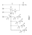
- FIG. 7 is a circuit diagram showing a configuration example of a pixel of a four-pixel sharing type solid-state imaging device including vertical two pixels and horizontal two pixels.
- FIG. 7 components corresponding to those in FIG. 3 are denoted by the same reference numerals, and thus detailed description thereof will be hereinafter omitted.
- four pixels 61 include PDs 71 , transfer transistors 72 , an FD 73 , a reset transistor 74 , amplification transistors 75 - 1 , 75 - 2 , and a selection transistor 76 .
- the FD 73 , the reset transistor 74 , the amplification transistors 75 - 1 , 75 - 2 , and the selection transistor 76 are shared by the four pixels 61 .
- FIGS. 8A, 8B are plan views showing a layout example of the four-pixel sharing type pixel 61 shown in FIG. 7 .
- components corresponding to those in FIG. 7 are denoted by the same reference numerals, and thus detailed description thereof will be hereinafter omitted.
- the amplification transistors 75 - 1 , 75 - 2 and the selection transistor 76 are formed on an identical active region.
- the amplification transistor 75 - 1 , the amplification transistor 75 - 2 , and the selection transistor 76 are formed on different active regions. Between each of the active regions, an element separation region is formed.
- the amplification transistors 75 - 1 , 75 - 2 are disposed not across a plurality of PDs 71 within a common pixel.
- the power sources Vdd connected to each of the amplification transistors 75 - 1 , 75 - 2 may be disposed in two places.
- the amplification transistors 75 - 1 , 75 - 2 are connected in parallel, which will be equivalent to a state that the gate width W of the amplification transistor is increased.
- the transconductance gm of the amplification transistor may be increased. As a result, a high frame rate image capture is possible without deteriorating the image quality.
- FIG. 9 is a circuit diagram showing other configuration example of a pixel sharing type pixel.
- FIG. 9 components corresponding to those in FIG. 7 are denoted by the same reference numerals, and thus detailed description thereof will be hereinafter omitted.
- the configuration shown in FIG. 9 is different from the configuration shown in FIG. 7 in that two selection transistors 76 - 1 , 76 - 2 are disposed instead of one selection transistor 76 .
- the amplification transistors 75 - 1 , 75 - 2 are connected to the vertical signal line 77 via the selection transistors 76 - 1 , 76 - 2 respectively.
- the selection transistors 760 - 1 , 76 - 2 are driven at the same time so as to output the signals read out by the amplification transistors 75 - 1 , 75 - 2 to the vertical signal line 77 .
- FIGS. 10A, 10B are plan views showing a layout example of the pixel sharing type pixel 61 shown in FIG. 9 .
- components corresponding to those in FIG. 9 are denoted by the same reference numerals, and thus detailed description thereof will be hereinafter omitted.
- the amplification transistors 75 - 1 , 75 - 2 and the selection transistors 76 - 1 , 76 - 2 are formed on an identical active region.
- the amplification transistor 75 - 1 and the selection transistor 76 - 1 , and the amplification transistor 75 - 2 and the selection transistor 76 - 2 are formed on different active regions. Between each of the active regions, an element separation region is formed.
- the amplification transistors 75 - 1 , 75 - 2 are disposed not across the plurality of PDs 71 within the common pixel.
- the power sources Vdd connected to each of the amplification transistors 75 - 1 , 75 - 2 may be disposed in two places.
- the amplification transistors 75 - 1 , 75 - 2 are connected in parallel, which will be equivalent to a state that the gate width W of the amplification transistor is increased.
- the transconductance gm of the amplification transistor may be increased. As a result, a high frame rate image capture is possible without deteriorating the image quality.
- two amplification transistors 75 - 1 , 75 - 2 are connected in parallel.
- Three or more amplification transistors may be connected in parallel.
- the number of the selection transistors connected to the plurality of amplification transistors connected in parallel may be the same or less as the amplification transistors. For example, when four amplification transistors are connected in parallel, four selection transistors may be provided that are connected to each of the four amplification transistors, or two selection transistors may be provided, one of them is connected to two amplification transistors.
- the transconductance gm of the amplification transistor may be increased.
- FIG. 11 is a circuit diagram showing a configuration example of a part of a pixel configuration in the related art. In FIG. 11 , only the amplification transistor 75 , the selection transistor 76 , and the constant current source 78 are shown.
- a drain current Isf is represented by the following equation (1).
- K is represented by a product ⁇ Cox of mobility ⁇ and a gate capacity Cox of the amplification transistor 75 .
- FIG. 12 is a circuit diagram showing a configuration example of a part of a pixel configuration including two amplification transistors connected in parallel.
- the amplification transistors 75 - 1 , 75 - 2 , the selection transistor 76 , and the constant current source 78 are shown.
- the amplification transistors 75 - 1 , 75 - 2 , the selection transistor 76 , and the constant current source 78 shown in FIG. 12 have the same specifications and properties as the amplification transistor 75 , the selection transistor 76 , and the constant current source 78 shown in FIG. 11 .
- a drain current Isf is represented by the following equation (2).
- the threshold voltage of the selection transistor is set lower than the threshold voltage of the plurality of the amplification transistors. In this manner, even when the plurality of the amplification transistors are connected in parallel, the voltage between AMP-SEL can be low, whereby it is possible to avoid the linearity deterioration of the selection transistor.
- the threshold voltage of the pixel transistor is controlled by a dope amount upon ion implantation of the transistor formation.
- the threshold voltage of the selection transistor is set lower than the threshold voltage of the amplification transistor, it is possible to avoid the linearity deterioration of the selection transistor.
- FIGS. 14A, 14B, 14C are views for explaining the on-resistance variation of the load MOS transistor as the constant current source.
- FIG. 14A is a circuit diagram showing a part of a pixel configuration including one amplification transistor, and the amplification transistor 75 , the selection transistor 76 , the vertical signal line 77 , and the constant current source 78 are shown.
- FIG. 14B is a circuit diagram showing an equivalent circuit shown in FIG. 14A .
- on-resistance of the amplification transistor 75 is represented by R_amp
- on-resistance of the selection transistor 76 is represented by R_sel
- on-resistance of the load MOS transistor as the constant current source 78 is represented by R_load
- a power supply voltage is represented by Vdd
- a source follower output Vout that is an output of the vertical signal line 77 is represented by the following equation (3).
- Vout R_load R_load + R_amp + R_sel ⁇ Vdd ( 3 )
- on-resistance R_amp of the amplification transistor 75 and on-resistance R_sel of the selection transistor 76 become small, as shown in FIG. 14C .
- the number of jags that are symbols showing the resistance represents a resistance value. The same applies to the following.
- the on-resistance of the load MOS transistor is set smaller than a sum of the on-resistance of the amplification transistor and the on-resistance of the selection transistor.
- the on-resistance R_load of the load MOS transistor shown in FIG. 15A is decreased as shown in FIG. 15B .
- the on-resistance R_amp of the amplification transistor 75 shown in FIG. 16A is increased as shown in FIG. 16B .
- the on-resistance R_amp of the amplification transistor 75 and the on-resistance R_sel of the selection transistor may be increased as shown in FIG. 17B .
- the on-resistance of the load MOS transistor becomes smaller relatively as compared to the on-resistance of the amplification transistor and the on-resistance of the selection transistor.
- the on-resistance of the load MOS transistor becomes not noticeable, and it is possible to inhibit a vertical streak from generating for the pixel column.
- An electronic apparatus 500 shown in FIG. 18 includes an optical lens 501 , a shutter apparatus 502 , a solid-state imaging device 503 , a driving circuit 504 , and a signal processing circuit 505 .
- FIG. 18 shows the configuration that the CMOS image sensor 50 having the pixels in the above-described embodiment is disposed at an electronic apparatus (for example, digital still camera) as the solid-state imaging device 503 .
- the optical lens 501 captures image light (incident light) from an object to be imaged on an imaging surface of the solid-state imaging device 503 . In this manner, a signal charge is accumulated for a certain period of time within the solid-state imaging device 503 .
- the shutter apparatus 502 controls a light irradiation period and a light shield period for the solid-state imaging device 503 .
- the driving circuit 504 supplies the driving signal that controls a signal transfer operation of the solid-state imaging device 503 and a shutter operation of the shutter apparatus 502 .
- the driving signal (timing signal) supplied from the driving circuit 504 the solid-state imaging device 503 performs a signal transfer.
- the signal processing circuit 505 performs a variety of signal processing to the signal output from the solid-state imaging device 503 .
- a video signal on which the signal processing is performed is stored in a storage medium such as a memory or is output to a monitor.
- the solid-state imaging device 503 can realize a high frame rate image capture without deteriorating the image quality. Therefore, it becomes possible to acquire a slow motion video and capture an object to be imaged that moves quickly in sports broadcasting or the like.
- the present technology may have the following configurations.
- a solid-state imaging device including:
- a vertical signal line to which the signal read out by the amplification transistor is output, the plurality of amplification transistors being connected in parallel.
- the selection transistor outputting the signal read out by the plurality of amplification transistors to the vertical signal line, in which
- the plurality of amplification transistors are connected to the vertical signal line via the selection transistor.
- the plurality of amplification transistors are formed on an identical active region.
- the plurality of amplification transistors are formed on different active regions, and
- an element separation region is formed between the different active regions.
- a threshold voltage of the selection transistor is set lower than a threshold voltage of the plurality of amplification transistors.
- on-resistance of the load transistor is set smaller than a sum of on-resistance of the plurality of amplification transistors and on-resistance of the selection transistor.
- the on-resistance of the load transistor is set smaller than the sum of the on-resistance of the plurality of amplification transistors and the on-resistance of the selection transistor by setting the threshold voltage of the load transistor lower.
- the on-resistance of the load transistor is set smaller than the sum of the on-resistance of the plurality of amplification transistors and the on-resistance of the selection transistor by setting the threshold voltage of the load transistor higher.
- the on-resistance of the load transistor is set smaller than the sum of the on-resistance of the plurality of amplification transistors and the on-resistance of the selection transistor by setting a load current value of the load transistor smaller.
- An electronic apparatus including:
- a solid-state imaging device including
Landscapes
- Engineering & Computer Science (AREA)
- Physics & Mathematics (AREA)
- Power Engineering (AREA)
- Electromagnetism (AREA)
- Condensed Matter Physics & Semiconductors (AREA)
- General Physics & Mathematics (AREA)
- Computer Hardware Design (AREA)
- Microelectronics & Electronic Packaging (AREA)
- Multimedia (AREA)
- Signal Processing (AREA)
- Solid State Image Pick-Up Elements (AREA)
- Transforming Light Signals Into Electric Signals (AREA)
Applications Claiming Priority (3)
| Application Number | Priority Date | Filing Date | Title |
|---|---|---|---|
| JP2014123238A JP2016005068A (ja) | 2014-06-16 | 2014-06-16 | 固体撮像装置および電子機器 |
| JP2014-123238 | 2014-06-16 | ||
| PCT/JP2015/066285 WO2015194390A1 (ja) | 2014-06-16 | 2015-06-05 | 固体撮像装置および電子機器 |
Related Parent Applications (1)
| Application Number | Title | Priority Date | Filing Date |
|---|---|---|---|
| PCT/JP2015/066285 A-371-Of-International WO2015194390A1 (ja) | 2014-06-16 | 2015-06-05 | 固体撮像装置および電子機器 |
Related Child Applications (1)
| Application Number | Title | Priority Date | Filing Date |
|---|---|---|---|
| US15/972,307 Continuation US10212376B2 (en) | 2014-06-16 | 2018-05-07 | Solid-state imaging device and electronic apparatus |
Publications (2)
| Publication Number | Publication Date |
|---|---|
| US20170201705A1 US20170201705A1 (en) | 2017-07-13 |
| US10027916B2 true US10027916B2 (en) | 2018-07-17 |
Family
ID=54935379
Family Applications (4)
| Application Number | Title | Priority Date | Filing Date |
|---|---|---|---|
| US15/314,976 Active US10027916B2 (en) | 2014-06-16 | 2015-06-05 | Solid-state imaging device and electronic apparatus |
| US15/972,307 Active US10212376B2 (en) | 2014-06-16 | 2018-05-07 | Solid-state imaging device and electronic apparatus |
| US16/208,962 Active US10491848B2 (en) | 2014-06-16 | 2018-12-04 | Solid-state imaging device and electronic apparatus |
| US16/671,647 Active US11012651B2 (en) | 2014-06-16 | 2019-11-01 | Solid-state imaging device and electronic apparatus |
Family Applications After (3)
| Application Number | Title | Priority Date | Filing Date |
|---|---|---|---|
| US15/972,307 Active US10212376B2 (en) | 2014-06-16 | 2018-05-07 | Solid-state imaging device and electronic apparatus |
| US16/208,962 Active US10491848B2 (en) | 2014-06-16 | 2018-12-04 | Solid-state imaging device and electronic apparatus |
| US16/671,647 Active US11012651B2 (en) | 2014-06-16 | 2019-11-01 | Solid-state imaging device and electronic apparatus |
Country Status (3)
| Country | Link |
|---|---|
| US (4) | US10027916B2 (ja) |
| JP (1) | JP2016005068A (ja) |
| WO (1) | WO2015194390A1 (ja) |
Cited By (3)
| Publication number | Priority date | Publication date | Assignee | Title |
|---|---|---|---|---|
| US10491848B2 (en) * | 2014-06-16 | 2019-11-26 | Sony Corporation | Solid-state imaging device and electronic apparatus |
| US11004879B2 (en) * | 2015-02-27 | 2021-05-11 | Sony Corporation | Semiconductor device, solid-state image pickup element, imaging device, and electronic apparatus |
| US11153523B2 (en) * | 2019-09-04 | 2021-10-19 | Canon Kabushiki Kaisha | Image capturing apparatus and method of controlling the same, and storage medium |
Families Citing this family (16)
| Publication number | Priority date | Publication date | Assignee | Title |
|---|---|---|---|---|
| JP6595804B2 (ja) * | 2015-05-27 | 2019-10-23 | ソニーセミコンダクタソリューションズ株式会社 | 固体撮像素子および撮像装置 |
| JP6706481B2 (ja) * | 2015-11-05 | 2020-06-10 | ソニーセミコンダクタソリューションズ株式会社 | 撮像素子 |
| KR20180076845A (ko) | 2016-12-28 | 2018-07-06 | 삼성전자주식회사 | 이미지 센서 |
| JP6815890B2 (ja) * | 2017-02-22 | 2021-01-20 | キヤノン株式会社 | 撮像装置、撮像システム、および、移動体 |
| JP6910814B2 (ja) * | 2017-02-22 | 2021-07-28 | ソニーセミコンダクタソリューションズ株式会社 | 固体撮像装置および電子機器 |
| KR102406996B1 (ko) | 2017-04-07 | 2022-06-08 | 삼성전자주식회사 | 이미지 센서 |
| JP2018207291A (ja) | 2017-06-05 | 2018-12-27 | ソニーセミコンダクタソリューションズ株式会社 | 固体撮像素子および撮像装置 |
| KR102356913B1 (ko) * | 2017-07-03 | 2022-02-03 | 에스케이하이닉스 주식회사 | 이미지 센서 |
| US10079261B1 (en) * | 2017-08-17 | 2018-09-18 | Omnivision Technologies, Inc. | Raised electrode to reduce dark current |
| KR102568744B1 (ko) * | 2018-01-29 | 2023-08-22 | 에스케이하이닉스 주식회사 | 이미지 센서 |
| JP7433863B2 (ja) | 2019-11-27 | 2024-02-20 | キヤノン株式会社 | 光電変換装置、撮像システム、および移動体 |
| US20230269503A1 (en) * | 2020-06-09 | 2023-08-24 | Sony Semiconductor Solutions Corporation | Solid-state imaging device |
| JP2022107201A (ja) * | 2021-01-08 | 2022-07-21 | ソニーセミコンダクタソリューションズ株式会社 | 撮像装置および電子機器 |
| DE112022001486T5 (de) * | 2021-03-15 | 2024-01-25 | Sony Semiconductor Solutions Corporation | Festkörperbildgebungsvorrichtung |
| JP2022149093A (ja) * | 2021-03-25 | 2022-10-06 | ソニーセミコンダクタソリューションズ株式会社 | 固体撮像装置および電子機器 |
| JP2023050707A (ja) * | 2021-09-30 | 2023-04-11 | ソニーセミコンダクタソリューションズ株式会社 | 固体撮像素子および電子機器 |
Citations (9)
| Publication number | Priority date | Publication date | Assignee | Title |
|---|---|---|---|---|
| JPH1126740A (ja) | 1997-06-30 | 1999-01-29 | Toshiba Corp | 固体撮像装置 |
| US20090033782A1 (en) * | 2007-07-31 | 2009-02-05 | Matsushita Electric Industrial Co., Ltd. | Solid-state imaging device and driving method thereof |
| US7858912B2 (en) * | 2002-08-16 | 2010-12-28 | The Hong Kong University Of Science And Technology | Ultra low voltage CMOS image sensor architecture |
| JP2011181595A (ja) | 2010-02-26 | 2011-09-15 | Panasonic Corp | 固体撮像装置およびカメラ |
| US20110273601A1 (en) * | 2010-05-07 | 2011-11-10 | Kabushiki Kaisha Toshiba | Solid-state imaging device |
| US20130050552A1 (en) * | 2011-08-24 | 2013-02-28 | Sony Corporation | Solid-state imaging apparatus, method of manufacturing solid-state imaging apparatus, and electronic apparatus |
| US20130049082A1 (en) * | 2011-08-22 | 2013-02-28 | Sony Corporation | Solid-state imaging device and electronic apparatus |
| US20130256509A1 (en) * | 2012-03-27 | 2013-10-03 | Omnivision Technologies, Inc. | Dual source follower pixel cell architecture |
| US20150103218A1 (en) * | 2007-11-15 | 2015-04-16 | Sony Corporation | Solid-state imaging device and camera system |
Family Cites Families (7)
| Publication number | Priority date | Publication date | Assignee | Title |
|---|---|---|---|---|
| JP4631723B2 (ja) * | 2006-01-27 | 2011-02-16 | ソニー株式会社 | 固体撮像装置 |
| JP5029624B2 (ja) * | 2009-01-15 | 2012-09-19 | ソニー株式会社 | 固体撮像装置及び電子機器 |
| JP6026102B2 (ja) * | 2011-12-07 | 2016-11-16 | ソニーセミコンダクタソリューションズ株式会社 | 固体撮像素子および電子機器 |
| JP2016012903A (ja) * | 2014-06-02 | 2016-01-21 | ソニー株式会社 | 撮像素子、撮像方法、および電子機器 |
| JP2016005068A (ja) * | 2014-06-16 | 2016-01-12 | ソニー株式会社 | 固体撮像装置および電子機器 |
| US9774801B2 (en) * | 2014-12-05 | 2017-09-26 | Qualcomm Incorporated | Solid state image sensor with enhanced charge capacity and dynamic range |
| KR20180076845A (ko) * | 2016-12-28 | 2018-07-06 | 삼성전자주식회사 | 이미지 센서 |
-
2014
- 2014-06-16 JP JP2014123238A patent/JP2016005068A/ja active Pending
-
2015
- 2015-06-05 WO PCT/JP2015/066285 patent/WO2015194390A1/ja active Application Filing
- 2015-06-05 US US15/314,976 patent/US10027916B2/en active Active
-
2018
- 2018-05-07 US US15/972,307 patent/US10212376B2/en active Active
- 2018-12-04 US US16/208,962 patent/US10491848B2/en active Active
-
2019
- 2019-11-01 US US16/671,647 patent/US11012651B2/en active Active
Patent Citations (12)
| Publication number | Priority date | Publication date | Assignee | Title |
|---|---|---|---|---|
| JPH1126740A (ja) | 1997-06-30 | 1999-01-29 | Toshiba Corp | 固体撮像装置 |
| US7858912B2 (en) * | 2002-08-16 | 2010-12-28 | The Hong Kong University Of Science And Technology | Ultra low voltage CMOS image sensor architecture |
| US20090033782A1 (en) * | 2007-07-31 | 2009-02-05 | Matsushita Electric Industrial Co., Ltd. | Solid-state imaging device and driving method thereof |
| US20150103218A1 (en) * | 2007-11-15 | 2015-04-16 | Sony Corporation | Solid-state imaging device and camera system |
| JP2011181595A (ja) | 2010-02-26 | 2011-09-15 | Panasonic Corp | 固体撮像装置およびカメラ |
| US20120314109A1 (en) * | 2010-02-26 | 2012-12-13 | Panasonic Corporation | Solid-state imaging device and camera |
| US20110273601A1 (en) * | 2010-05-07 | 2011-11-10 | Kabushiki Kaisha Toshiba | Solid-state imaging device |
| US20130049082A1 (en) * | 2011-08-22 | 2013-02-28 | Sony Corporation | Solid-state imaging device and electronic apparatus |
| JP2013062789A (ja) | 2011-08-22 | 2013-04-04 | Sony Corp | 固体撮像装置及び電子機器 |
| US20130050552A1 (en) * | 2011-08-24 | 2013-02-28 | Sony Corporation | Solid-state imaging apparatus, method of manufacturing solid-state imaging apparatus, and electronic apparatus |
| JP2013045878A (ja) | 2011-08-24 | 2013-03-04 | Sony Corp | 固体撮像装置、固体撮像装置の製造方法、電子機器 |
| US20130256509A1 (en) * | 2012-03-27 | 2013-10-03 | Omnivision Technologies, Inc. | Dual source follower pixel cell architecture |
Cited By (4)
| Publication number | Priority date | Publication date | Assignee | Title |
|---|---|---|---|---|
| US10491848B2 (en) * | 2014-06-16 | 2019-11-26 | Sony Corporation | Solid-state imaging device and electronic apparatus |
| US11012651B2 (en) | 2014-06-16 | 2021-05-18 | Sony Corporation | Solid-state imaging device and electronic apparatus |
| US11004879B2 (en) * | 2015-02-27 | 2021-05-11 | Sony Corporation | Semiconductor device, solid-state image pickup element, imaging device, and electronic apparatus |
| US11153523B2 (en) * | 2019-09-04 | 2021-10-19 | Canon Kabushiki Kaisha | Image capturing apparatus and method of controlling the same, and storage medium |
Also Published As
| Publication number | Publication date |
|---|---|
| WO2015194390A1 (ja) | 2015-12-23 |
| US20170201705A1 (en) | 2017-07-13 |
| US10491848B2 (en) | 2019-11-26 |
| US20190110014A1 (en) | 2019-04-11 |
| US20180255261A1 (en) | 2018-09-06 |
| US20200068159A1 (en) | 2020-02-27 |
| US10212376B2 (en) | 2019-02-19 |
| JP2016005068A (ja) | 2016-01-12 |
| US11012651B2 (en) | 2021-05-18 |
Similar Documents
| Publication | Publication Date | Title |
|---|---|---|
| US11012651B2 (en) | Solid-state imaging device and electronic apparatus | |
| US10171760B2 (en) | Solid-state imaging device, method for driving solid-state imaging device, and electronic apparatus using an amplifier and signal lines for low and high gain | |
| US9992417B2 (en) | Solid-state imaging device, method for driving solid-state imaging device, and electronic apparatus | |
| JP6541523B2 (ja) | 撮像装置、撮像システム、および、撮像装置の制御方法 | |
| US8289425B2 (en) | Solid-state image pickup device with an improved output amplifier circuitry | |
| JP6045156B2 (ja) | 固体撮像装置 | |
| US8294798B2 (en) | Solid-state imaging apparatus | |
| CN106341627B (zh) | 摄像装置 | |
| US8023022B2 (en) | Solid-state imaging apparatus | |
| JP2006073733A (ja) | 固体撮像装置及び固体撮像システム | |
| US20130248939A1 (en) | Solid-state imaging apparatus | |
| WO2010089838A1 (ja) | 固体撮像装置及びカメラ | |
| JP2007150008A (ja) | 固体撮像装置 | |
| JP2014187270A (ja) | 固体撮像装置およびその製造方法、並びに電子機器 | |
| US8040416B2 (en) | Solid-state imaging apparatus | |
| JP5012782B2 (ja) | 撮像装置 | |
| JP5190185B2 (ja) | 固体撮像装置および撮像装置 | |
| WO2017022451A1 (ja) | 固体撮像装置および電子機器 | |
| JP2007129473A (ja) | 固体撮像装置及び撮像システム | |
| JP4720402B2 (ja) | 固体撮像装置 | |
| JP2012151692A (ja) | 固体撮像装置及びこれを備えた撮像システム | |
| US10602088B2 (en) | Solid-state imaging device and imaging apparatus | |
| CN114391249A (zh) | 固态成像元件和电子设备 | |
| JP2013121058A (ja) | 固体撮像装置、撮像装置、および信号読み出し方法 | |
| US20150334330A1 (en) | Solid-state image capture device and image capture device |
Legal Events
| Date | Code | Title | Description |
|---|---|---|---|
| AS | Assignment |
Owner name: SONY CORPORATION, JAPAN Free format text: ASSIGNMENT OF ASSIGNORS INTEREST;ASSIGNOR:ISHIWATA, HIROAKI;REEL/FRAME:040747/0289 Effective date: 20161107 |
|
| STCF | Information on status: patent grant |
Free format text: PATENTED CASE |
|
| MAFP | Maintenance fee payment |
Free format text: PAYMENT OF MAINTENANCE FEE, 4TH YEAR, LARGE ENTITY (ORIGINAL EVENT CODE: M1551); ENTITY STATUS OF PATENT OWNER: LARGE ENTITY Year of fee payment: 4 |