KR950000205B1 - 리이드 프레임 및 이를 사용한 반도체 장치 - Google Patents
리이드 프레임 및 이를 사용한 반도체 장치 Download PDFInfo
- Publication number
- KR950000205B1 KR950000205B1 KR1019860007396A KR860007396A KR950000205B1 KR 950000205 B1 KR950000205 B1 KR 950000205B1 KR 1019860007396 A KR1019860007396 A KR 1019860007396A KR 860007396 A KR860007396 A KR 860007396A KR 950000205 B1 KR950000205 B1 KR 950000205B1
- Authority
- KR
- South Korea
- Prior art keywords
- lead
- tab
- integrated circuit
- semiconductor integrated
- circuit device
- Prior art date
Links
Images


Classifications
-
- H—ELECTRICITY
- H01—ELECTRIC ELEMENTS
- H01L—SEMICONDUCTOR DEVICES NOT COVERED BY CLASS H10
- H01L23/00—Details of semiconductor or other solid state devices
- H01L23/48—Arrangements for conducting electric current to or from the solid state body in operation, e.g. leads, terminal arrangements ; Selection of materials therefor
-
- H—ELECTRICITY
- H01—ELECTRIC ELEMENTS
- H01L—SEMICONDUCTOR DEVICES NOT COVERED BY CLASS H10
- H01L21/00—Processes or apparatus adapted for the manufacture or treatment of semiconductor or solid state devices or of parts thereof
- H01L21/02—Manufacture or treatment of semiconductor devices or of parts thereof
- H01L21/04—Manufacture or treatment of semiconductor devices or of parts thereof the devices having at least one potential-jump barrier or surface barrier, e.g. PN junction, depletion layer or carrier concentration layer
- H01L21/48—Manufacture or treatment of parts, e.g. containers, prior to assembly of the devices, using processes not provided for in a single one of the subgroups H01L21/06 - H01L21/326
- H01L21/4814—Conductive parts
- H01L21/4821—Flat leads, e.g. lead frames with or without insulating supports
- H01L21/4825—Connection or disconnection of other leads to or from flat leads, e.g. wires, bumps, other flat leads
-
- H—ELECTRICITY
- H01—ELECTRIC ELEMENTS
- H01L—SEMICONDUCTOR DEVICES NOT COVERED BY CLASS H10
- H01L23/00—Details of semiconductor or other solid state devices
- H01L23/48—Arrangements for conducting electric current to or from the solid state body in operation, e.g. leads, terminal arrangements ; Selection of materials therefor
- H01L23/488—Arrangements for conducting electric current to or from the solid state body in operation, e.g. leads, terminal arrangements ; Selection of materials therefor consisting of soldered or bonded constructions
- H01L23/495—Lead-frames or other flat leads
- H01L23/49541—Geometry of the lead-frame
-
- H—ELECTRICITY
- H01—ELECTRIC ELEMENTS
- H01L—SEMICONDUCTOR DEVICES NOT COVERED BY CLASS H10
- H01L24/00—Arrangements for connecting or disconnecting semiconductor or solid-state bodies; Methods or apparatus related thereto
- H01L24/01—Means for bonding being attached to, or being formed on, the surface to be connected, e.g. chip-to-package, die-attach, "first-level" interconnects; Manufacturing methods related thereto
- H01L24/42—Wire connectors; Manufacturing methods related thereto
- H01L24/47—Structure, shape, material or disposition of the wire connectors after the connecting process
- H01L24/48—Structure, shape, material or disposition of the wire connectors after the connecting process of an individual wire connector
-
- H—ELECTRICITY
- H01—ELECTRIC ELEMENTS
- H01L—SEMICONDUCTOR DEVICES NOT COVERED BY CLASS H10
- H01L24/00—Arrangements for connecting or disconnecting semiconductor or solid-state bodies; Methods or apparatus related thereto
- H01L24/01—Means for bonding being attached to, or being formed on, the surface to be connected, e.g. chip-to-package, die-attach, "first-level" interconnects; Manufacturing methods related thereto
- H01L24/42—Wire connectors; Manufacturing methods related thereto
- H01L24/47—Structure, shape, material or disposition of the wire connectors after the connecting process
- H01L24/49—Structure, shape, material or disposition of the wire connectors after the connecting process of a plurality of wire connectors
-
- H—ELECTRICITY
- H01—ELECTRIC ELEMENTS
- H01L—SEMICONDUCTOR DEVICES NOT COVERED BY CLASS H10
- H01L2224/00—Indexing scheme for arrangements for connecting or disconnecting semiconductor or solid-state bodies and methods related thereto as covered by H01L24/00
- H01L2224/01—Means for bonding being attached to, or being formed on, the surface to be connected, e.g. chip-to-package, die-attach, "first-level" interconnects; Manufacturing methods related thereto
- H01L2224/02—Bonding areas; Manufacturing methods related thereto
- H01L2224/04—Structure, shape, material or disposition of the bonding areas prior to the connecting process
- H01L2224/05—Structure, shape, material or disposition of the bonding areas prior to the connecting process of an individual bonding area
- H01L2224/0554—External layer
- H01L2224/0555—Shape
- H01L2224/05552—Shape in top view
- H01L2224/05554—Shape in top view being square
-
- H—ELECTRICITY
- H01—ELECTRIC ELEMENTS
- H01L—SEMICONDUCTOR DEVICES NOT COVERED BY CLASS H10
- H01L2224/00—Indexing scheme for arrangements for connecting or disconnecting semiconductor or solid-state bodies and methods related thereto as covered by H01L24/00
- H01L2224/01—Means for bonding being attached to, or being formed on, the surface to be connected, e.g. chip-to-package, die-attach, "first-level" interconnects; Manufacturing methods related thereto
- H01L2224/26—Layer connectors, e.g. plate connectors, solder or adhesive layers; Manufacturing methods related thereto
- H01L2224/31—Structure, shape, material or disposition of the layer connectors after the connecting process
- H01L2224/32—Structure, shape, material or disposition of the layer connectors after the connecting process of an individual layer connector
- H01L2224/321—Disposition
- H01L2224/32151—Disposition the layer connector connecting between a semiconductor or solid-state body and an item not being a semiconductor or solid-state body, e.g. chip-to-substrate, chip-to-passive
- H01L2224/32221—Disposition the layer connector connecting between a semiconductor or solid-state body and an item not being a semiconductor or solid-state body, e.g. chip-to-substrate, chip-to-passive the body and the item being stacked
- H01L2224/32245—Disposition the layer connector connecting between a semiconductor or solid-state body and an item not being a semiconductor or solid-state body, e.g. chip-to-substrate, chip-to-passive the body and the item being stacked the item being metallic
-
- H—ELECTRICITY
- H01—ELECTRIC ELEMENTS
- H01L—SEMICONDUCTOR DEVICES NOT COVERED BY CLASS H10
- H01L2224/00—Indexing scheme for arrangements for connecting or disconnecting semiconductor or solid-state bodies and methods related thereto as covered by H01L24/00
- H01L2224/01—Means for bonding being attached to, or being formed on, the surface to be connected, e.g. chip-to-package, die-attach, "first-level" interconnects; Manufacturing methods related thereto
- H01L2224/42—Wire connectors; Manufacturing methods related thereto
- H01L2224/44—Structure, shape, material or disposition of the wire connectors prior to the connecting process
- H01L2224/45—Structure, shape, material or disposition of the wire connectors prior to the connecting process of an individual wire connector
- H01L2224/45001—Core members of the connector
- H01L2224/45099—Material
- H01L2224/451—Material with a principal constituent of the material being a metal or a metalloid, e.g. boron (B), silicon (Si), germanium (Ge), arsenic (As), antimony (Sb), tellurium (Te) and polonium (Po), and alloys thereof
- H01L2224/45138—Material with a principal constituent of the material being a metal or a metalloid, e.g. boron (B), silicon (Si), germanium (Ge), arsenic (As), antimony (Sb), tellurium (Te) and polonium (Po), and alloys thereof the principal constituent melting at a temperature of greater than or equal to 950°C and less than 1550°C
- H01L2224/45144—Gold (Au) as principal constituent
-
- H—ELECTRICITY
- H01—ELECTRIC ELEMENTS
- H01L—SEMICONDUCTOR DEVICES NOT COVERED BY CLASS H10
- H01L2224/00—Indexing scheme for arrangements for connecting or disconnecting semiconductor or solid-state bodies and methods related thereto as covered by H01L24/00
- H01L2224/01—Means for bonding being attached to, or being formed on, the surface to be connected, e.g. chip-to-package, die-attach, "first-level" interconnects; Manufacturing methods related thereto
- H01L2224/42—Wire connectors; Manufacturing methods related thereto
- H01L2224/47—Structure, shape, material or disposition of the wire connectors after the connecting process
- H01L2224/48—Structure, shape, material or disposition of the wire connectors after the connecting process of an individual wire connector
- H01L2224/4805—Shape
- H01L2224/4809—Loop shape
- H01L2224/48091—Arched
-
- H—ELECTRICITY
- H01—ELECTRIC ELEMENTS
- H01L—SEMICONDUCTOR DEVICES NOT COVERED BY CLASS H10
- H01L2224/00—Indexing scheme for arrangements for connecting or disconnecting semiconductor or solid-state bodies and methods related thereto as covered by H01L24/00
- H01L2224/01—Means for bonding being attached to, or being formed on, the surface to be connected, e.g. chip-to-package, die-attach, "first-level" interconnects; Manufacturing methods related thereto
- H01L2224/42—Wire connectors; Manufacturing methods related thereto
- H01L2224/47—Structure, shape, material or disposition of the wire connectors after the connecting process
- H01L2224/48—Structure, shape, material or disposition of the wire connectors after the connecting process of an individual wire connector
- H01L2224/481—Disposition
- H01L2224/48151—Connecting between a semiconductor or solid-state body and an item not being a semiconductor or solid-state body, e.g. chip-to-substrate, chip-to-passive
- H01L2224/48221—Connecting between a semiconductor or solid-state body and an item not being a semiconductor or solid-state body, e.g. chip-to-substrate, chip-to-passive the body and the item being stacked
- H01L2224/48245—Connecting between a semiconductor or solid-state body and an item not being a semiconductor or solid-state body, e.g. chip-to-substrate, chip-to-passive the body and the item being stacked the item being metallic
- H01L2224/48247—Connecting between a semiconductor or solid-state body and an item not being a semiconductor or solid-state body, e.g. chip-to-substrate, chip-to-passive the body and the item being stacked the item being metallic connecting the wire to a bond pad of the item
-
- H—ELECTRICITY
- H01—ELECTRIC ELEMENTS
- H01L—SEMICONDUCTOR DEVICES NOT COVERED BY CLASS H10
- H01L2224/00—Indexing scheme for arrangements for connecting or disconnecting semiconductor or solid-state bodies and methods related thereto as covered by H01L24/00
- H01L2224/01—Means for bonding being attached to, or being formed on, the surface to be connected, e.g. chip-to-package, die-attach, "first-level" interconnects; Manufacturing methods related thereto
- H01L2224/42—Wire connectors; Manufacturing methods related thereto
- H01L2224/47—Structure, shape, material or disposition of the wire connectors after the connecting process
- H01L2224/48—Structure, shape, material or disposition of the wire connectors after the connecting process of an individual wire connector
- H01L2224/484—Connecting portions
- H01L2224/48463—Connecting portions the connecting portion on the bonding area of the semiconductor or solid-state body being a ball bond
- H01L2224/48465—Connecting portions the connecting portion on the bonding area of the semiconductor or solid-state body being a ball bond the other connecting portion not on the bonding area being a wedge bond, i.e. ball-to-wedge, regular stitch
-
- H—ELECTRICITY
- H01—ELECTRIC ELEMENTS
- H01L—SEMICONDUCTOR DEVICES NOT COVERED BY CLASS H10
- H01L2224/00—Indexing scheme for arrangements for connecting or disconnecting semiconductor or solid-state bodies and methods related thereto as covered by H01L24/00
- H01L2224/01—Means for bonding being attached to, or being formed on, the surface to be connected, e.g. chip-to-package, die-attach, "first-level" interconnects; Manufacturing methods related thereto
- H01L2224/42—Wire connectors; Manufacturing methods related thereto
- H01L2224/47—Structure, shape, material or disposition of the wire connectors after the connecting process
- H01L2224/48—Structure, shape, material or disposition of the wire connectors after the connecting process of an individual wire connector
- H01L2224/485—Material
- H01L2224/48505—Material at the bonding interface
- H01L2224/48599—Principal constituent of the connecting portion of the wire connector being Gold (Au)
-
- H—ELECTRICITY
- H01—ELECTRIC ELEMENTS
- H01L—SEMICONDUCTOR DEVICES NOT COVERED BY CLASS H10
- H01L2224/00—Indexing scheme for arrangements for connecting or disconnecting semiconductor or solid-state bodies and methods related thereto as covered by H01L24/00
- H01L2224/01—Means for bonding being attached to, or being formed on, the surface to be connected, e.g. chip-to-package, die-attach, "first-level" interconnects; Manufacturing methods related thereto
- H01L2224/42—Wire connectors; Manufacturing methods related thereto
- H01L2224/47—Structure, shape, material or disposition of the wire connectors after the connecting process
- H01L2224/49—Structure, shape, material or disposition of the wire connectors after the connecting process of a plurality of wire connectors
- H01L2224/491—Disposition
- H01L2224/4912—Layout
- H01L2224/49171—Fan-out arrangements
-
- H—ELECTRICITY
- H01—ELECTRIC ELEMENTS
- H01L—SEMICONDUCTOR DEVICES NOT COVERED BY CLASS H10
- H01L2224/00—Indexing scheme for arrangements for connecting or disconnecting semiconductor or solid-state bodies and methods related thereto as covered by H01L24/00
- H01L2224/01—Means for bonding being attached to, or being formed on, the surface to be connected, e.g. chip-to-package, die-attach, "first-level" interconnects; Manufacturing methods related thereto
- H01L2224/42—Wire connectors; Manufacturing methods related thereto
- H01L2224/47—Structure, shape, material or disposition of the wire connectors after the connecting process
- H01L2224/49—Structure, shape, material or disposition of the wire connectors after the connecting process of a plurality of wire connectors
- H01L2224/491—Disposition
- H01L2224/4912—Layout
- H01L2224/49175—Parallel arrangements
-
- H—ELECTRICITY
- H01—ELECTRIC ELEMENTS
- H01L—SEMICONDUCTOR DEVICES NOT COVERED BY CLASS H10
- H01L2224/00—Indexing scheme for arrangements for connecting or disconnecting semiconductor or solid-state bodies and methods related thereto as covered by H01L24/00
- H01L2224/01—Means for bonding being attached to, or being formed on, the surface to be connected, e.g. chip-to-package, die-attach, "first-level" interconnects; Manufacturing methods related thereto
- H01L2224/42—Wire connectors; Manufacturing methods related thereto
- H01L2224/47—Structure, shape, material or disposition of the wire connectors after the connecting process
- H01L2224/49—Structure, shape, material or disposition of the wire connectors after the connecting process of a plurality of wire connectors
- H01L2224/491—Disposition
- H01L2224/4912—Layout
- H01L2224/49177—Combinations of different arrangements
- H01L2224/49179—Corner adaptations, i.e. disposition of the wire connectors at the corners of the semiconductor or solid-state body
-
- H—ELECTRICITY
- H01—ELECTRIC ELEMENTS
- H01L—SEMICONDUCTOR DEVICES NOT COVERED BY CLASS H10
- H01L2224/00—Indexing scheme for arrangements for connecting or disconnecting semiconductor or solid-state bodies and methods related thereto as covered by H01L24/00
- H01L2224/73—Means for bonding being of different types provided for in two or more of groups H01L2224/10, H01L2224/18, H01L2224/26, H01L2224/34, H01L2224/42, H01L2224/50, H01L2224/63, H01L2224/71
- H01L2224/732—Location after the connecting process
- H01L2224/73251—Location after the connecting process on different surfaces
- H01L2224/73265—Layer and wire connectors
-
- H—ELECTRICITY
- H01—ELECTRIC ELEMENTS
- H01L—SEMICONDUCTOR DEVICES NOT COVERED BY CLASS H10
- H01L2224/00—Indexing scheme for arrangements for connecting or disconnecting semiconductor or solid-state bodies and methods related thereto as covered by H01L24/00
- H01L2224/74—Apparatus for manufacturing arrangements for connecting or disconnecting semiconductor or solid-state bodies and for methods related thereto
- H01L2224/78—Apparatus for connecting with wire connectors
- H01L2224/7825—Means for applying energy, e.g. heating means
- H01L2224/783—Means for applying energy, e.g. heating means by means of pressure
- H01L2224/78301—Capillary
-
- H—ELECTRICITY
- H01—ELECTRIC ELEMENTS
- H01L—SEMICONDUCTOR DEVICES NOT COVERED BY CLASS H10
- H01L2224/00—Indexing scheme for arrangements for connecting or disconnecting semiconductor or solid-state bodies and methods related thereto as covered by H01L24/00
- H01L2224/80—Methods for connecting semiconductor or other solid state bodies using means for bonding being attached to, or being formed on, the surface to be connected
- H01L2224/85—Methods for connecting semiconductor or other solid state bodies using means for bonding being attached to, or being formed on, the surface to be connected using a wire connector
- H01L2224/85009—Pre-treatment of the connector or the bonding area
- H01L2224/8503—Reshaping, e.g. forming the ball or the wedge of the wire connector
- H01L2224/85035—Reshaping, e.g. forming the ball or the wedge of the wire connector by heating means, e.g. "free-air-ball"
- H01L2224/85043—Reshaping, e.g. forming the ball or the wedge of the wire connector by heating means, e.g. "free-air-ball" using a flame torch, e.g. hydrogen torch
-
- H—ELECTRICITY
- H01—ELECTRIC ELEMENTS
- H01L—SEMICONDUCTOR DEVICES NOT COVERED BY CLASS H10
- H01L2224/00—Indexing scheme for arrangements for connecting or disconnecting semiconductor or solid-state bodies and methods related thereto as covered by H01L24/00
- H01L2224/80—Methods for connecting semiconductor or other solid state bodies using means for bonding being attached to, or being formed on, the surface to be connected
- H01L2224/85—Methods for connecting semiconductor or other solid state bodies using means for bonding being attached to, or being formed on, the surface to be connected using a wire connector
- H01L2224/85009—Pre-treatment of the connector or the bonding area
- H01L2224/8503—Reshaping, e.g. forming the ball or the wedge of the wire connector
- H01L2224/85035—Reshaping, e.g. forming the ball or the wedge of the wire connector by heating means, e.g. "free-air-ball"
- H01L2224/85045—Reshaping, e.g. forming the ball or the wedge of the wire connector by heating means, e.g. "free-air-ball" using a corona discharge, e.g. electronic flame off [EFO]
-
- H—ELECTRICITY
- H01—ELECTRIC ELEMENTS
- H01L—SEMICONDUCTOR DEVICES NOT COVERED BY CLASS H10
- H01L2224/00—Indexing scheme for arrangements for connecting or disconnecting semiconductor or solid-state bodies and methods related thereto as covered by H01L24/00
- H01L2224/80—Methods for connecting semiconductor or other solid state bodies using means for bonding being attached to, or being formed on, the surface to be connected
- H01L2224/85—Methods for connecting semiconductor or other solid state bodies using means for bonding being attached to, or being formed on, the surface to be connected using a wire connector
- H01L2224/8512—Aligning
- H01L2224/85148—Aligning involving movement of a part of the bonding apparatus
- H01L2224/85169—Aligning involving movement of a part of the bonding apparatus being the upper part of the bonding apparatus, i.e. bonding head, e.g. capillary or wedge
- H01L2224/8518—Translational movements
- H01L2224/85181—Translational movements connecting first on the semiconductor or solid-state body, i.e. on-chip, regular stitch
-
- H—ELECTRICITY
- H01—ELECTRIC ELEMENTS
- H01L—SEMICONDUCTOR DEVICES NOT COVERED BY CLASS H10
- H01L24/00—Arrangements for connecting or disconnecting semiconductor or solid-state bodies; Methods or apparatus related thereto
- H01L24/01—Means for bonding being attached to, or being formed on, the surface to be connected, e.g. chip-to-package, die-attach, "first-level" interconnects; Manufacturing methods related thereto
- H01L24/42—Wire connectors; Manufacturing methods related thereto
- H01L24/44—Structure, shape, material or disposition of the wire connectors prior to the connecting process
- H01L24/45—Structure, shape, material or disposition of the wire connectors prior to the connecting process of an individual wire connector
-
- H—ELECTRICITY
- H01—ELECTRIC ELEMENTS
- H01L—SEMICONDUCTOR DEVICES NOT COVERED BY CLASS H10
- H01L2924/00—Indexing scheme for arrangements or methods for connecting or disconnecting semiconductor or solid-state bodies as covered by H01L24/00
- H01L2924/0001—Technical content checked by a classifier
- H01L2924/00014—Technical content checked by a classifier the subject-matter covered by the group, the symbol of which is combined with the symbol of this group, being disclosed without further technical details
-
- H—ELECTRICITY
- H01—ELECTRIC ELEMENTS
- H01L—SEMICONDUCTOR DEVICES NOT COVERED BY CLASS H10
- H01L2924/00—Indexing scheme for arrangements or methods for connecting or disconnecting semiconductor or solid-state bodies as covered by H01L24/00
- H01L2924/01—Chemical elements
- H01L2924/01005—Boron [B]
-
- H—ELECTRICITY
- H01—ELECTRIC ELEMENTS
- H01L—SEMICONDUCTOR DEVICES NOT COVERED BY CLASS H10
- H01L2924/00—Indexing scheme for arrangements or methods for connecting or disconnecting semiconductor or solid-state bodies as covered by H01L24/00
- H01L2924/01—Chemical elements
- H01L2924/01014—Silicon [Si]
-
- H—ELECTRICITY
- H01—ELECTRIC ELEMENTS
- H01L—SEMICONDUCTOR DEVICES NOT COVERED BY CLASS H10
- H01L2924/00—Indexing scheme for arrangements or methods for connecting or disconnecting semiconductor or solid-state bodies as covered by H01L24/00
- H01L2924/01—Chemical elements
- H01L2924/01015—Phosphorus [P]
-
- H—ELECTRICITY
- H01—ELECTRIC ELEMENTS
- H01L—SEMICONDUCTOR DEVICES NOT COVERED BY CLASS H10
- H01L2924/00—Indexing scheme for arrangements or methods for connecting or disconnecting semiconductor or solid-state bodies as covered by H01L24/00
- H01L2924/01—Chemical elements
- H01L2924/01027—Cobalt [Co]
-
- H—ELECTRICITY
- H01—ELECTRIC ELEMENTS
- H01L—SEMICONDUCTOR DEVICES NOT COVERED BY CLASS H10
- H01L2924/00—Indexing scheme for arrangements or methods for connecting or disconnecting semiconductor or solid-state bodies as covered by H01L24/00
- H01L2924/01—Chemical elements
- H01L2924/01028—Nickel [Ni]
-
- H—ELECTRICITY
- H01—ELECTRIC ELEMENTS
- H01L—SEMICONDUCTOR DEVICES NOT COVERED BY CLASS H10
- H01L2924/00—Indexing scheme for arrangements or methods for connecting or disconnecting semiconductor or solid-state bodies as covered by H01L24/00
- H01L2924/01—Chemical elements
- H01L2924/01078—Platinum [Pt]
-
- H—ELECTRICITY
- H01—ELECTRIC ELEMENTS
- H01L—SEMICONDUCTOR DEVICES NOT COVERED BY CLASS H10
- H01L2924/00—Indexing scheme for arrangements or methods for connecting or disconnecting semiconductor or solid-state bodies as covered by H01L24/00
- H01L2924/01—Chemical elements
- H01L2924/01079—Gold [Au]
-
- H—ELECTRICITY
- H01—ELECTRIC ELEMENTS
- H01L—SEMICONDUCTOR DEVICES NOT COVERED BY CLASS H10
- H01L2924/00—Indexing scheme for arrangements or methods for connecting or disconnecting semiconductor or solid-state bodies as covered by H01L24/00
- H01L2924/10—Details of semiconductor or other solid state devices to be connected
- H01L2924/1015—Shape
- H01L2924/1016—Shape being a cuboid
- H01L2924/10162—Shape being a cuboid with a square active surface
-
- H—ELECTRICITY
- H01—ELECTRIC ELEMENTS
- H01L—SEMICONDUCTOR DEVICES NOT COVERED BY CLASS H10
- H01L2924/00—Indexing scheme for arrangements or methods for connecting or disconnecting semiconductor or solid-state bodies as covered by H01L24/00
- H01L2924/10—Details of semiconductor or other solid state devices to be connected
- H01L2924/11—Device type
- H01L2924/14—Integrated circuits
-
- H—ELECTRICITY
- H01—ELECTRIC ELEMENTS
- H01L—SEMICONDUCTOR DEVICES NOT COVERED BY CLASS H10
- H01L2924/00—Indexing scheme for arrangements or methods for connecting or disconnecting semiconductor or solid-state bodies as covered by H01L24/00
- H01L2924/15—Details of package parts other than the semiconductor or other solid state devices to be connected
- H01L2924/181—Encapsulation
Abstract
내용 없음.
Description
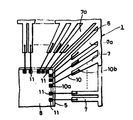
제 1 도는 본 발명의 실시예 1인 리이드 프레임에 펠릿 와이어 본딩이 실시된 것을 도시한 확대부분 평면도.
제 2 도는 실시예 1의 리이드 프레임의 전체를 도시한 평면도.
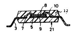
제 3 도는 실시예 1의 리이드 프레임을 사용한 반도체 장치를 도시한 전체 단면도.
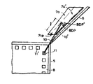
제 4 도는 본딩시의 리이드 프레임 및 그 주변의 단면도.
제 5 도는 본딩시의 리이프 프레임의 평면도.
제 6 도는 본 발명의 실시예 2인 리이드 프레임에 펠릿 본딩, 와이어 본딩이 실시된 것을 도시한 확대부분 평면도.
본 발명은 리이드 프레임 및 이를 사용한 반도체 장치에 관한 것으로, 특히 반도체 장치의 제조공정에 있어서의 와이어 본딩의 높은 신뢰성 및 작업성 향상이 도모되는 유효한 기술에 관한 것이다.
펠릿과 내부 리이드의 전기적 도통을 도모하는 기술의 하나로서, 소위 와이어 본딩법이 있다. 이 와이어 본딩법에서는, 예를들어 우선 금(Au)과 같은 금속으로 되는 본딩 와이어의 선단부분을 방전가공, 수소(H2) 토오치(torch) 등에 의해 가열하여 용융하고, 그 선단부분에 볼(ball)을 형성하고, 그 볼부분을 펠릿의 본딩패드전극에 눌러서 제 1본딩을 실행한다. 다음에, 상기 와이어가 루프를 형성하도록 본딩용 캐필러리를 내부 리이드위의 소정의 부위에 위치시키고, 본딩 와이어를 내부 리이드에 누르는 것에 의해서 제 2본딩을 실행한다. 최후로, 본딩 와이어의 나머지 부분을 절단하여 본딩을 완료하는 것이다.
그런데, 플래트 패키지(flat package)형의 반도체 장치에 사용되는 리이드 프레임인 경우, 탭의 모서리 부분에 탭서스펜딩 리이드(이하, 탭걸이 리이드라 한다)가 배치되어 있고, 다 핀화를 포함하는 내부 리이드(여러개의 내부 리이드가 마련되어 있는 것)에서는 탭의 모서리 부분 근방, 즉 탭걸이 리이드(탭을 리이드 프레임의 프레임에 연결하여 탭을 지지하고 있는 리이드)에 가깝게 마련되어 있는 내부 리이드와 펠릿의 패드전극과의 거리가 크게 떨어지게 되므로, 이에 따라서 본딩 와이어의 인장거리도 길어지게 된다. 이로 인해, 본딩 와이어에 느슨함을 일으키기 쉽고, 본딩 와이어와 다른 내부 리이드 또는 본딩 와이어와 탭걸이 리이드 등과의 전기적 쇼트를 일으키기 쉬운 것이 본 발명자에 의해서 발견되었다.
또 탭걸이 리이드에 인접해서 마련되어 있는 내부 리이드가 다른 내부 리이드와 같은 리이드폭 및 같은 리이드 길이를 갖고 있지 않을 경우의 와이어 본딩시는 상기 리이드 프레임에 있어서의 탭모서리 부분에 결합하고 있는 탭걸이 리이드 가까이의 내부 리이드 위쪽에서 본딩 와이어가 떨어지는 일이 일어난다. 이로인해, 제 2본딩에 의한 와이어의 지지가 불충분하게 되고, 이것이 와이어의 느슨함의 한 원인이 되는 것도 본 발명자에 의해서 명확하게 되었다.
그리고, 와이어 본딩의 기술로서 상세하게 기술되어 있는 예로써는 일본국 (주)공업조사회, 1980년 1월15일 발행, 「IC화 실장 기술」(일본국 Microelectronics 협회편), p99∼p103이 있다.
본 발명의 목적은 와이어 본딩시의 와이어의 쇼트를 방지하여 신뢰성을 높일 수가 있는 리이드 프레임을 제공하는데 있다.
본 발명의 다른 목적은 전기적으로 신뢰성이 높은 반도체 장치를 제공하는데 있다.
본 발명의 상기 및 그외의 목적과 새로운 특징은 본 명세서의 기술 및 첨부도면에서 명확하게 될 것이다.
본 출원에 있어서 개시되는 발명중 대표적인 것의 개요를 간단히 설명하면 다음과 같다.
즉, 탭걸이 리이드에 인접해서 마련된 내부 리이드의 폭 또는 길이가 다른 내부 리이드보다 크게 되도록 형성되는 리이드 프레임 구조로 하는 것에 의해 제 2본딩에 있어서 와이어의 지지가 충분하게 되므로, 본딩을 확실하게 실행할 수가 있어 와이어의 쇼트의 발생을 방지할 수가 있다.
또, 상기 기술에 의해 전기적 신뢰성이 높은 반도체 장치를 제공할 수가 있다.
[실시예 1]
제 1 도는 본 발명의 1실시예인 리이드 프레임에 펠릿 본딩, 와이어 본딩이 실시된 것을 도시한 확대부분 평면도, 제 2 도는 리이드 프레임의 전체를 도시한 평면도, 제 3 도는 이 리이드 프레임을 사용한 반도체 장치를 도시한 전체 단면도, 제 4 도는 본딩시의 리이드 프레임 및 그 주변부분의 단면도이다.
본 실시예 1의 리이드 프레임(1)은 특별히 제한되지 않으나, 제 3 도에 도시한 것과 같은 수지 봉지형의 플래트 패키지, 소위 FPP(Flat Plastic Package)형의 반도체 장치(21)에 사용되는 리이드 프레임이며, 제 2 도에 도시한 형상의 것을 1단위로 하여 좌우 양방향으로 여러단위를 연결한 형상으로 되는 것이다.
리이드 프레임(1)은 사각형상의 프레임부(2)와 그 프레임부(2)의 각변에서 중앙방향으로 각각 연장되어 마련된 여러개의 리이드(3) 및 그 각 리이드의 도중부분을 서로 연결하는 타이 바(tie bar)(4)를 갖고 있다. 또, 리이드 프레임(1)의 중앙부분에는 사각형상의 탭(5)이 형성되어 있고, 이 탭(5)은 그 4개의 모서리와 상기 프레임부(2)의 4개의 모서리를 각각 연결하는 탭걸이 리이드(6)에 의해서 지지되어 있다. 상기 타이 바(4)에 둘러싸인 리이드(3)의 부분은 내부 리이드(7)을 형성하고 있으며, 이 내부 리이드(7)의 적어도 선단부분의 표면에는 본딩을 양호하게 실행하기 위하여 금(Au)등의 도시하지 않은 도금층이 형성되어 있다. 본 실시예 1에 따르면, 상기 탭걸이 리이드(6)에 인접해서 마련되는 내부 리이드(7a)는 제 1 도와 같은 다른 내부 리이드(7)보다도 폭이 넓게 형성되어 있다.
이와같은 리이드 프레임(1)은, 예를들면 동(Cu), 니켈 42%, 철(Fe) 58%의 합금인 42합금 또는 철 53%, 니켈 28%, 코발트 18%로 되는 합금인 코발(coval) 등으로 되는 얇은 판상의 금속판에 에칭처리 또는 프레스처리 등을 실시하여 소정의 형상으로 가공하는 것에 의해서 얻어지는 것이다.
이와같이 하여 얻어진 리이드 프레임(1)에는 우선 그 탭(5) 위에 실리콘 반도체로 되는 펠릿(8)이 접착제(9)에 의해서 피착된다.
이와같은 펠릿이 피착된 리이드 프레임은 다음에 도시하지 않은 와이어 본딩장치의 본딩 스테이지 위에 탑재되어 금(Au) 등으로 되는 가는선 형상의 본딩 와이어(10)에 의해 펠릿(8)의 본딩 패드전극(11)과 내부 리이드(7)의 결선, 즉 와이어 본딩이 실행된다. 이 와이어 본딩 공정에서는 우선 상기 와이어(10)의 한쪽끝을 방전가공 등에 의해 가열 용융하는 것에 의해서 볼이 형성된다. 다음에, 와이어를 지지하는 본딩용 캐필러리(와이어 접속 공구)(60)이 반도체 펠릿의 본딩 패드(11)위로 이동되어 제 4도의 화살표 a와 같이 강하된다. 이로 인해서, 볼(10a)부분이 패드(11)에 압착되어 제 1본딩이 실행된다.
다음에, 와이어(10)이 루프를 형성하도록 캐필러리(60)이 이동되어 제 2본딩이 실행된다. 즉, 제 1본딩후에 캐필러리(60)이 제 4 도의 화살표 b로 나타낸 바와같이 상승되어 화살표 C로 나타낸 바와같이 내부 리이드(7a)의 본딩 에리어를 향해서 수평 이동되며, 이어서 화살표 d로 나타낸 바와같이 하강된다.
와이어(10)을 내부 리이드(7a)에 열압착시키는 누르는 힘이 캐필러리(60)에 의해서 와이어(10)에 가해지고, 그 결과 와이어 본딩이 실행된다. 그후, 캐필러리(60)이 제 4 도의 화살표 e와 같이 상승된다. 이때 와이어 본딩장치에 있어서의 도시하지 않은 와이어 클램프 기구가 동작되고, 캐필러리(60)쪽의 와이어(10')는 그 와이어 클램프 기구에 의해서 인장응력이 가해져서 제 4 도에 도시한 바와같이 전단(shear)된다.
이로 인해서, 1사이클의 본딩 공정이 완료된다. 이상의 공정 소정회수만큼 반복하는 것에 의해서 필요로 하는 모든 패드(11)와 내부 리이드(7)가 접속되게 된다.
본 실시예 1에 의하면, 탭걸이 리이드(6)에 인접해서 마련된 내부 리이드(7a)가 상술한 것과 같이 다른 리이드(7)보다도 폭이 넓게 형성되어 있다. 따라서, 제 2본딩시에 그 내부 리이드(7a)에 대해서 루프를 추적하면서 착지되는 와이어(10)에 대하여 충분한 접촉 폭을 확보할 수가 있다. 따라서, 탭걸이 리이드(6)에 인접해서 마련된 내부 리이드(7a)에 결합되는 와이어에 일어나기 쉬운 와이어(10)의 늘어짐을 효과적으로 방지할 수가 있어 와이어(10)의 쇼트의 발생을 방지할 수가 있다.
와이어(10)의 쇼트 방지에 대하여 제 4 도의 단면도 및 제 5 도의 평면도에 따라서 상세하게 설명하면 다음과 같이 된다.
즉, 내부 리이드(7a)의 선단(7tp)에서 내부 리이드(7a)의 본딩 위치 BDP까지의 평면부분 거리l은 와이어(10)의 루프형상의 바라지 않는 변형을 방지하는데 유효한 부분으로 된다. 본 실시예와 같은 탭걸이 리이드(6)에 인접하는 내부 리이드(7a)의 폭이 넓게 되어 있는 경우, 와이어(10)는 반도체 펠릿(8)의 본딩되어야 할 패드(11)의 위치가 다소 변경되어도 제 5 도에 실선으로 도시한 바와같이 내부 리이드의 선단위를 통과하게 된다. 이 경우는 와이어(10)의 본딩시의 리이드 쪽으로의 루프가 부분l에 의해서 양호하게 제한된다. 그 결과, 와이어(10)는 제 4의 실선으로 나타낸 바와같이, 실질적으로 리이드의 평면보다 위부분에만 위치되게 되어 바라지 않는 쇼트를 일으키는 일이 없다.
이에 대해서, 내부 리이드(7a)가 제 5 도에 2점 쇄선으로 나타낸 바와같이, 좁은 폭을 갖도록 되어있을 경우, 즉 종래의 리이드 프레임에 있어서의 경우, 이때에 마련되는 와이어(10')는 제 5 도의 점선으로 나타낸 바와같이, 패드(11)의 위치의 약간의 변경에 의해서도 내부 리이드의 선단부 위를 벗어나서 연장되게 된다. 이 경우, 내부 리이드의 부분l은 와이어(10')의 루프의 바람직하지 않는 변형을 충분히 방지할 수가 없게된다. 이것에 따라서, 와이어(10')는 제 4 도에 2점 쇄선으로 나타낸 바와같이, 리이드의 주면보다 아래쪽으로 연장하는 루프를 형성할 우려가 생긴다.
그리고, 와이어 본딩시에 내부 리이드의 선단과 탭(5)의 둘레의 공간에 돌기를 배치하는 것은 와이어의 루프의 바라지 않는 변형을 방지하는데 의미가 있다. 제 4 도에 있어서, 점선(50)은 와이어 본딩장치에 있어서의 워크 스테이션 또는 리이드 프레임용 테이블로서의 히트 블록(heat block)을 도시하고 있다. 이 경우의 히트 블록은 상술의 목적은 돌기(51)을 갖는다. 탭걸이 리이드(6)에서 떨어진 내부 리이드와 패드를 결합하는 본딩 와이어는 만약 내부 리이드의 폭이 좁아도 그 루프 형상이 돌기(51)에 의해서 양호하게 된다. 이 경우, 탭걸이 리이드(6)에 인접하는 내부 리이드와 패드를 결합하는 와이어에 대한 돌기(51)의 효과는 다음의 이유에 의해서 실질적으로 기대할 수 없다.
즉, 돌기(51)에 대한 탭걸이 리이드(6)의 위치는, 예를들면 워크 스테이션에 대한 리이드 프레임의 위치 맞춤정도에 의해서 영향을 받게 된다. 탭걸이 리이드(6)의 위치의 다소의 변동에도 불구하고 탭걸이 리이드(6)가 돌기(51)에 걸리지 않도록 하기 위하여 돌기(51)은 그것과 탭걸이 리이드(6) 사이에 비교적 큰 공간이 생기도록 크게 된다. 그 결과로서, 탭걸이 리이드(6)에 인접하는 내부 리이드(7a)와 탭(5)와의 사이에 돌기(51)를 연장시키는 것이 곤란하게 되므로, 그 리이드(7a)에 결합되는 와이어의 형상을 돌기(51)로 규정하여 성형할 수는 없다.
다음의 공정으로서 와이어 본딩이 완료된 리이드 프레임(1)은 트랜스퍼 몰드(transfer mold)법에 의해 에폭시 수지(12)로 수지봉지되고, 패키징이 실행된후, 각 리이드(3)가 독립상태로 절단·성형되어서 제 3 도에 도시한 FPP형의 반도체 장치(21)을 얻을 수가 있다.
[실시예 2]
제 6 도는 본 발명의 다른 실시예인 리이드 프레임을 도시한 확대부분 평면도이다.
본 실시예 2의 리이드 프레임(41)은 실시예 1에서 설명한 리이드 프레임(1)과 대략 마찬가지이지만, 그 차이점은 탭걸이 리이드(6)에 인접해서 마련된 내부 리이드(47a)의 형상을 다르게 한 것이다.
즉, 이 리이드 프레임(41)에서는 탭걸이 리이드(6)에 인접해서 마련된 내부 리이드(47a)가 다른 내부 리이드(47)보다 축방향에 대해서 길게 형성되고, 그 리이드 선단은 탭(5)의 아주 가까이까지 연장되어 있다. 구체적으로는 내부 리이드(47a)와 탭의 떨어지는 거리가 다른 내부 리이드와 탭의 떨어지는 거리에 비해서 동일하던가, 그 이하의 길이이다. 이로 인해, 와이어 본딩을 할 때에는 와이어(10)의 인장거리를 짧게 할 수가 있다. 따라서, 탭걸이 리이드(6)에 인접해서 마련된 내부 리이드(47a)에 일어나기 쉬운 와이어(10)의 늘어짐을 방지할 수가 있어 와이어의 쇼트를 방지하여 전기적 신뢰성이 높은 반도체 장치를 제공할 수가 있다.
본 발명은 다음에 기술하는 여러 가지 효과가 있다.
(1) 탭걸이 리이드에 인접하여 마련된 내부 리이드가 다른 내부 리이드보다 와이어와의 본딩 면적이 크도록 형성되는 리이드 프레임 구조로 하는 것에 의해 제 2본딩에 있어서 와이어의 착지시에 충분한 활주거리를 확보할 수가 있으므로, 본딩을 확실하게 실행할 수가 있어 와이어의 쇼트를 방지할 수가 있다.
(2) 탭걸이 리이드에 인접해서 마련된 내부 리이드가 다른 리이드보다도 길게 하여 이루어지는 리이드 프레임 구조로 하는 것에 의해, 본딩 와이어의 루프길이를 짧게 할 수 있다. 이로 인해, 인접하는 리이드와 본딩 와이어와의 쇼트를 방지할 수가 있다.
(3) 상기 (1), (2)에 의해, 전기적 신뢰성이 높은 반도체 장치를 제공할 수가 있다.
(4) 상기 (1), (2)에 의해 내부 리이드가 미세화되었을 경우에 있어서도 탭걸이 리이드에 인접해서 마련된 내부 리이드에서의 와이어의 늘어짐을 방지할 수가 있으므로, 와이어 본딩의 신뢰성을 향상시켜서 반도체 장치의 높은 집적화를 촉진할 수가 있다.
이상 본 발명자에 의해서 이루어진 발명을 실시예에 따라서 구체적으로 설명하였으나, 본 발명은 상기 실시예에 한정되는 것은 아니며, 그 요지를 이탈하지 않는 범위에서 여러 가지로 변경이 가능하다는 것을 말할 것도 없다.
예를들면, 탭걸이 리이드에 인접해서 마련된 내부 리이드의 형상으로서 폭 또는 축 방향길이를 크게 한 경우에 대해서만 설명하였으나, 이러한 형상에 한정하지 않으며, 어떠한 형상이라도 면적을 크게 한 것이면 좋다.
또, 실시예에서는 FPP형의 반도체 장치에 사용되는 리이드 프레임에 대해서만 설명하였으나, 이에 한정되지 않으며, 외부 리이드를 J자 형상으로 성형하는 소위 PLCC(Plastic leaded Chip Carrier)형의 반도체 장치에 사용되는 리이드 프레임이라도 좋다.
또한, 본딩 방법에 대해서도 와이어 본딩 에너지가 초음파 진동만으로 와이어의 접합을 실행하는 소위 웨지 본딩이라도 좋다.
실시예와 같이, 탭걸이 리이드(6)에 인접하는 내부 리이드(7a)의 폭을 증대시키는 경우에는 그것에 따라서 내부 리이드(7a)에 대한 본딩 가능 범위를 넓게 설정할 수가 있게 된다. 이로 인해서, 반도체 펠릿의 본딩되어야 할 패드 전극의 위치가 변경되었을 경우에도 이에 따라서 내부 리이드(7a)의 본딩 위치를 변경할 수가 있게 되어 와이어가 내부 리이드(7a)의 선단부 위를 통과하도록 할 수가 있다.
그러나, 이러한 내부 리이드(7a)는, 예를들면 부채형, T자형의 평면 패턴과 같이 실질적으로 그 선단부만이 폭이 넓혀져도 좋다. 이 경우에도 와이어 루프의 바라지 않는 형상을 없앨 수가 있다.
이상의 설명에서는 주로 본 발명자에 의해서 이루어진 발명을 그 이용분야인, 소위 수지 봉지형의 반도체 장치에 적용한 경우에 대해서 설명하였으나, 이에 한정되는 것은 아니며, 예를들면 저융점의 유리 등을 봉지재로 사용한 기밀봉지형의 반도체 장치에 적용하여도 유효한 기술이다.
Claims (13)
- 탭에 연결되고, 그곳에서 멀어지는 방향을 향해서 연장하는 적어도 3개의 탭걸이 리이드, 제 1의 면에 여러개의 본딩패드를 갖고, 제 2의 면에서 상기 탭에 접착되어 있는 반도체칩, 각각이 탭의 주변근방에 위치하는 자유단을 갖는 내부 리이드부와 외부 리이드부로 이루어지는 여러개의 리이드, 상기 본딩패드와 상기 자유단사이를 각각 전기적으로 접속하고 있는 본딩 와이어 및 상기 칩, 탭, 내부 리이드부, 본딩 와이어를 통하여 막고 있는 봉지재를 포함하는 반도체 장치에 있어서, 상기 내부 리이드부는 탭과 동일평면에 있으며, 적어도 각각의 자유단에서 가는 리이드와 상기 탭걸이 리이드의 근방에 배치되어 있는 폭이 넓은 리이드로 이루어지는 것을 특징으로 하는 반도체집적회로장치.
- 특허청구의 범위 제 1 항에 있어서, 상기 봉지재는 수지인 것을 특징으로 하는 반도체집적회로장치.
- 특허청구의 범위 제 1 항에 있어서, 상기 봉지재는 기밀봉지체인 것을 특징으로 하는 반도체집적회로 장치.
- 특허청구의 범위 제 1항에 있어서, 상기 봉지재는 판형상의 봉지체이고, 상기 칩, 텝, 내부 리이드부 및 본딩 와이어를 포함하는 평면에 평행한 1쌍의 주면을 갖는 것을 특징으로 하는 반도체집적회로장치.
- 특허청구의 범위 제 1 항 내지 제 4 항중의 어느 한 항에 있어서, 각각의 탭걸이 리이드 근방의 모두가 폭이 넓은 리이드이고, 그 이외는 가는 리이드인 것을 특징으로 하는 반도체집적회로장치.
- 특허청구의 범위 제 1 항에 있어서, 상기 탭과 탭걸이 리이드는 금속시이트에 의해서 일체로 성형되어 있는 것을 특징으로 하는 반도체집적회로장치.
- 특허청구의 범위 제 1 항에 있어서, 상기 탭걸이 리이드는 각각 서로 직행하는 3개의 다른 방향을 향해서 연장하고 있는 것을 특징으로 하는 반도체집적회로장치.
- 특허청구의 범위 제 1 항에 있어서, 상기 탭은 4각형상이고, 3개의 탭걸이 리이드는 탭의 모서리부에서 멀어지는 방향을 향해서 연장하고 있는 것을 특징으로 하는 반도체집적회로장치.
- 특허청구의 범위 제 8 항에 있어서, 4개의 탭걸이 리이드가 4개의 모서리부에서 멀어지는 방향을 향해서 연장하고 있는 것을 특징으로 하는 반도체집적회로장치.
- 특허청구의 범위 제 1 항 또는 제 2 항에 있어서, 상기 탭과 상기 폭이 넓은 리이드의 거리는 탭과 상기 가는 리이드의 거리와 동일하던가 또는 짧은 것을 특징으로 하는 반도체집적회로장치.
- 특허청구의 범위 제 5 항에 있어서, 상기 폭이 넓은 리이드는 상기 가는 리이드와 비교해서 폭이 넓은 것을 특징으로 하는 반도체집적회로장치.
- 특허청구의 범위 제 6 항 내지 제 9 항중의 어느 한 항에 있어서, 상기 폭이 넓은 리이드는 상기 가는 리이드와 비교해서 폭이 넓은 것을 특징으로 하는 반도체집적회로장치.
- 특허청구의 범위 제 10 항에 있어서, 상기 폭이 넓은 리이드는 상기 가는 리이드와 비교해서 폭이 넓은 것을 특징으로 하는 반도체집적회로장치.
Applications Claiming Priority (2)
| Application Number | Priority Date | Filing Date | Title |
|---|---|---|---|
| JP60221832A JPS6281738A (ja) | 1985-10-07 | 1985-10-07 | リ−ドフレ−ムおよびそれを用いた半導体装置 |
| JP60-221832 | 1985-10-07 |
Publications (2)
| Publication Number | Publication Date |
|---|---|
| KR870004509A KR870004509A (ko) | 1987-05-11 |
| KR950000205B1 true KR950000205B1 (ko) | 1995-01-11 |
Family
ID=16772889
Family Applications (1)
| Application Number | Title | Priority Date | Filing Date |
|---|---|---|---|
| KR1019860007396A KR950000205B1 (ko) | 1985-10-07 | 1986-09-04 | 리이드 프레임 및 이를 사용한 반도체 장치 |
Country Status (3)
| Country | Link |
|---|---|
| US (1) | US4951120A (ko) |
| JP (1) | JPS6281738A (ko) |
| KR (1) | KR950000205B1 (ko) |
Families Citing this family (17)
| Publication number | Priority date | Publication date | Assignee | Title |
|---|---|---|---|---|
| JPS6281738A (ja) * | 1985-10-07 | 1987-04-15 | Hitachi Micro Comput Eng Ltd | リ−ドフレ−ムおよびそれを用いた半導体装置 |
| KR100195850B1 (ko) * | 1990-03-13 | 1999-06-15 | 구라우치 노리타카 | 광모듈과 그 제조 공정 |
| US5053852A (en) * | 1990-07-05 | 1991-10-01 | At&T Bell Laboratories | Molded hybrid IC package and lead frame therefore |
| US5061988A (en) * | 1990-07-30 | 1991-10-29 | Mcdonnell Douglas Corporation | Integrated circuit chip interconnect |
| JPH04213867A (ja) * | 1990-11-27 | 1992-08-04 | Ibiden Co Ltd | 電子部品搭載用基板フレーム |
| JPH05218233A (ja) * | 1992-02-06 | 1993-08-27 | Mitsubishi Electric Corp | 半導体装置およびその製造方法 |
| JP2714335B2 (ja) * | 1992-12-16 | 1998-02-16 | 株式会社東芝 | 半導体装置 |
| US5322207A (en) * | 1993-05-03 | 1994-06-21 | Micron Semiconductor Inc. | Method and apparatus for wire bonding semiconductor dice to a leadframe |
| US5350106A (en) | 1993-05-07 | 1994-09-27 | Micron Semiconductor, Inc. | Semiconductor wire bonding method |
| JP2542795B2 (ja) * | 1994-09-22 | 1996-10-09 | 九州日本電気株式会社 | 樹脂封止型半導体装置 |
| US5781682A (en) * | 1996-02-01 | 1998-07-14 | International Business Machines Corporation | Low-cost packaging for parallel optical computer link |
| US5611478A (en) * | 1996-03-11 | 1997-03-18 | National Semiconductor Corporation | Lead frame clamp for ultrasonic bonding |
| JP3638750B2 (ja) * | 1997-03-25 | 2005-04-13 | 株式会社ルネサステクノロジ | 半導体装置 |
| JP2000082717A (ja) * | 1998-09-07 | 2000-03-21 | Shinkawa Ltd | ワイヤボンディング方法 |
| US6847099B1 (en) * | 2003-02-05 | 2005-01-25 | Amkor Technology Inc. | Offset etched corner leads for semiconductor package |
| JP2006210862A (ja) * | 2004-12-27 | 2006-08-10 | Toshiba Corp | 半導体用リードフレーム、メモリカードおよび半導体装置 |
| US7466516B2 (en) * | 2005-01-28 | 2008-12-16 | Hitachi Global Storage Technologies Netherlands B.V. | Lead configuration for reduced capacitive interference in a magnetic read/write head |
Family Cites Families (13)
| Publication number | Priority date | Publication date | Assignee | Title |
|---|---|---|---|---|
| NL7018378A (ko) * | 1970-12-17 | 1972-06-20 | ||
| JPS5431470B2 (ko) * | 1971-12-15 | 1979-10-06 | ||
| JPS5431470U (ko) * | 1977-08-05 | 1979-03-01 | ||
| JPS5521128A (en) * | 1978-08-02 | 1980-02-15 | Hitachi Ltd | Lead frame used for semiconductor device and its assembling |
| JPS5648161A (en) * | 1979-09-26 | 1981-05-01 | Nec Kyushu Ltd | Lead frame for semiconductor device |
| JPS5674948A (en) * | 1979-11-22 | 1981-06-20 | Hitachi Ltd | Lead structure of semiconductor device |
| JPS56116654A (en) * | 1980-02-20 | 1981-09-12 | Nec Corp | Manufacturing of lead frame for semiconductor device |
| JPS5758777U (ko) * | 1980-09-24 | 1982-04-07 | ||
| JPS5861654A (ja) * | 1981-10-09 | 1983-04-12 | Toshiba Corp | 半導体装置 |
| JPS58142554A (ja) * | 1982-02-19 | 1983-08-24 | Hitachi Ltd | リ−ドフレ−ム |
| JPS61269345A (ja) * | 1985-05-24 | 1986-11-28 | Hitachi Ltd | 半導体装置 |
| JP2559364B2 (ja) * | 1985-07-12 | 1996-12-04 | 株式会社日立製作所 | 半導体装置用リ−ドフレ−ム |
| JPS6281738A (ja) * | 1985-10-07 | 1987-04-15 | Hitachi Micro Comput Eng Ltd | リ−ドフレ−ムおよびそれを用いた半導体装置 |
-
1985
- 1985-10-07 JP JP60221832A patent/JPS6281738A/ja active Granted
-
1986
- 1986-09-04 KR KR1019860007396A patent/KR950000205B1/ko not_active IP Right Cessation
-
1988
- 1988-12-13 US US07/283,842 patent/US4951120A/en not_active Expired - Lifetime
Also Published As
| Publication number | Publication date |
|---|---|
| JPH0455341B2 (ko) | 1992-09-03 |
| JPS6281738A (ja) | 1987-04-15 |
| KR870004509A (ko) | 1987-05-11 |
| US4951120A (en) | 1990-08-21 |
Similar Documents
| Publication | Publication Date | Title |
|---|---|---|
| US5793108A (en) | Semiconductor integrated circuit having a plurality of semiconductor chips | |
| US9905497B2 (en) | Resin sealing type semiconductor device and method of manufacturing the same, and lead frame | |
| KR950000205B1 (ko) | 리이드 프레임 및 이를 사용한 반도체 장치 | |
| JP4294161B2 (ja) | スタックパッケージ及びその製造方法 | |
| JP5564392B2 (ja) | 半導体装置 | |
| US5834691A (en) | Lead frame, its use in the fabrication of resin-encapsulated semiconductor device | |
| US9087827B2 (en) | Mixed wire semiconductor lead frame package | |
| US7274092B2 (en) | Semiconductor component and method of assembling the same | |
| US20060125065A1 (en) | Multi-part lead frame with dissimilar materials | |
| US6777262B2 (en) | Method of packaging a semiconductor device having gull-wing leads with thinner end portions | |
| US6340837B1 (en) | Semiconductor device and method of fabricating the same | |
| JP3638750B2 (ja) | 半導体装置 | |
| JPS60167454A (ja) | 半導体装置 | |
| US5708295A (en) | Lead frame and method of manufacturing the same, and resin sealed semiconductor device and method of manufacturing the same | |
| CN109087903B (zh) | 电子装置、用于电子装置的引线框架以及制造电子装置和引线框架的方法 | |
| JP3497775B2 (ja) | 半導体装置 | |
| JPH04503283A (ja) | 半導体チップを含むインダクタンスの小さいカプセル封じパッケージ | |
| JP3419898B2 (ja) | 半導体装置及びその製造方法 | |
| JPH0525236Y2 (ko) | ||
| JPH02197158A (ja) | リードフレームの製造方法 | |
| JP4764608B2 (ja) | 半導体装置 | |
| JPH07193180A (ja) | 樹脂封止型半導体装置 | |
| JPH0936295A (ja) | リードフレームおよびその製造方法ならびに樹脂封止型半導体装置およびその製造方法 | |
| JPH0846122A (ja) | リードピンおよびその製造方法 | |
| JPH06163801A (ja) | 樹脂封止型半導体装置 |
Legal Events
| Date | Code | Title | Description |
|---|---|---|---|
| A201 | Request for examination | ||
| G160 | Decision to publish patent application | ||
| E701 | Decision to grant or registration of patent right | ||
| GRNT | Written decision to grant | ||
| FPAY | Annual fee payment |
Payment date: 20040112 Year of fee payment: 10 |
|
| LAPS | Lapse due to unpaid annual fee |