KR20200019269A - Semiconductor device - Google Patents
Semiconductor device Download PDFInfo
- Publication number
- KR20200019269A KR20200019269A KR1020207004429A KR20207004429A KR20200019269A KR 20200019269 A KR20200019269 A KR 20200019269A KR 1020207004429 A KR1020207004429 A KR 1020207004429A KR 20207004429 A KR20207004429 A KR 20207004429A KR 20200019269 A KR20200019269 A KR 20200019269A
- Authority
- KR
- South Korea
- Prior art keywords
- film
- insulating film
- oxide semiconductor
- transistor
- semiconductor film
- Prior art date
Links
- 239000004065 semiconductor Substances 0.000 title claims abstract description 400
- QGZKDVFQNNGYKY-UHFFFAOYSA-N Ammonia Chemical compound N QGZKDVFQNNGYKY-UHFFFAOYSA-N 0.000 claims abstract description 130
- IJGRMHOSHXDMSA-UHFFFAOYSA-N Atomic nitrogen Chemical compound N#N IJGRMHOSHXDMSA-UHFFFAOYSA-N 0.000 claims abstract description 124
- 239000001257 hydrogen Substances 0.000 claims abstract description 101
- 229910052739 hydrogen Inorganic materials 0.000 claims abstract description 101
- 150000004767 nitrides Chemical class 0.000 claims abstract description 99
- UFHFLCQGNIYNRP-UHFFFAOYSA-N Hydrogen Chemical compound [H][H] UFHFLCQGNIYNRP-UHFFFAOYSA-N 0.000 claims abstract description 90
- 229910021529 ammonia Inorganic materials 0.000 claims abstract description 65
- 229910052757 nitrogen Inorganic materials 0.000 claims abstract description 62
- 238000004868 gas analysis Methods 0.000 claims abstract description 17
- 229910052760 oxygen Inorganic materials 0.000 claims description 133
- 239000001301 oxygen Substances 0.000 claims description 133
- QVGXLLKOCUKJST-UHFFFAOYSA-N atomic oxygen Chemical compound [O] QVGXLLKOCUKJST-UHFFFAOYSA-N 0.000 claims description 132
- 238000000034 method Methods 0.000 claims description 109
- 239000007789 gas Substances 0.000 claims description 68
- 229910052710 silicon Inorganic materials 0.000 claims description 65
- 239000010703 silicon Substances 0.000 claims description 65
- 238000005268 plasma chemical vapour deposition Methods 0.000 claims description 24
- 239000012298 atmosphere Substances 0.000 claims description 22
- 238000004519 manufacturing process Methods 0.000 claims description 22
- 238000003795 desorption Methods 0.000 claims description 10
- 238000000151 deposition Methods 0.000 claims description 8
- 230000008021 deposition Effects 0.000 claims description 8
- 239000010408 film Substances 0.000 description 1019
- 239000000758 substrate Substances 0.000 description 125
- 229910052581 Si3N4 Inorganic materials 0.000 description 70
- HQVNEWCFYHHQES-UHFFFAOYSA-N silicon nitride Chemical compound N12[Si]34N5[Si]62N3[Si]51N64 HQVNEWCFYHHQES-UHFFFAOYSA-N 0.000 description 70
- XUIMIQQOPSSXEZ-UHFFFAOYSA-N Silicon Chemical compound [Si] XUIMIQQOPSSXEZ-UHFFFAOYSA-N 0.000 description 63
- 229910044991 metal oxide Inorganic materials 0.000 description 56
- 239000011701 zinc Substances 0.000 description 55
- 150000004706 metal oxides Chemical class 0.000 description 54
- XLYOFNOQVPJJNP-UHFFFAOYSA-N water Substances O XLYOFNOQVPJJNP-UHFFFAOYSA-N 0.000 description 53
- 229910001868 water Inorganic materials 0.000 description 53
- 238000010438 heat treatment Methods 0.000 description 46
- 230000002829 reductive effect Effects 0.000 description 38
- 239000000203 mixture Substances 0.000 description 36
- 239000010410 layer Substances 0.000 description 34
- 239000013078 crystal Substances 0.000 description 33
- 239000004973 liquid crystal related substance Substances 0.000 description 33
- 238000012545 processing Methods 0.000 description 31
- 230000008569 process Effects 0.000 description 30
- 238000004544 sputter deposition Methods 0.000 description 29
- 125000004429 atom Chemical group 0.000 description 28
- 238000004458 analytical method Methods 0.000 description 26
- 239000000463 material Substances 0.000 description 26
- 239000002585 base Substances 0.000 description 25
- 239000012535 impurity Substances 0.000 description 24
- 239000003566 sealing material Substances 0.000 description 23
- 229910052751 metal Inorganic materials 0.000 description 22
- 230000006870 function Effects 0.000 description 21
- 230000015572 biosynthetic process Effects 0.000 description 20
- 230000007547 defect Effects 0.000 description 20
- 239000002184 metal Substances 0.000 description 19
- 239000010936 titanium Substances 0.000 description 19
- RTAQQCXQSZGOHL-UHFFFAOYSA-N Titanium Chemical compound [Ti] RTAQQCXQSZGOHL-UHFFFAOYSA-N 0.000 description 18
- 229910052782 aluminium Inorganic materials 0.000 description 18
- XAGFODPZIPBFFR-UHFFFAOYSA-N aluminium Chemical compound [Al] XAGFODPZIPBFFR-UHFFFAOYSA-N 0.000 description 18
- VYPSYNLAJGMNEJ-UHFFFAOYSA-N silicon dioxide Inorganic materials O=[Si]=O VYPSYNLAJGMNEJ-UHFFFAOYSA-N 0.000 description 18
- 229910052814 silicon oxide Inorganic materials 0.000 description 18
- 229910052719 titanium Inorganic materials 0.000 description 18
- 229910052721 tungsten Inorganic materials 0.000 description 16
- 239000010937 tungsten Substances 0.000 description 16
- 238000010586 diagram Methods 0.000 description 15
- WFKWXMTUELFFGS-UHFFFAOYSA-N tungsten Chemical compound [W] WFKWXMTUELFFGS-UHFFFAOYSA-N 0.000 description 15
- XLOMVQKBTHCTTD-UHFFFAOYSA-N Zinc monoxide Chemical compound [Zn]=O XLOMVQKBTHCTTD-UHFFFAOYSA-N 0.000 description 14
- 230000001681 protective effect Effects 0.000 description 14
- BLRPTPMANUNPDV-UHFFFAOYSA-N Silane Chemical compound [SiH4] BLRPTPMANUNPDV-UHFFFAOYSA-N 0.000 description 13
- 238000005401 electroluminescence Methods 0.000 description 13
- -1 hydrogen Chemical compound 0.000 description 13
- 150000002431 hydrogen Chemical class 0.000 description 13
- 239000012071 phase Substances 0.000 description 13
- 229920005989 resin Polymers 0.000 description 13
- 239000011347 resin Substances 0.000 description 13
- 229910000077 silane Inorganic materials 0.000 description 13
- 206010021143 Hypoxia Diseases 0.000 description 12
- GQPLMRYTRLFLPF-UHFFFAOYSA-N Nitrous Oxide Chemical compound [O-][N+]#N GQPLMRYTRLFLPF-UHFFFAOYSA-N 0.000 description 12
- 229910021417 amorphous silicon Inorganic materials 0.000 description 11
- 230000003287 optical effect Effects 0.000 description 11
- 238000012360 testing method Methods 0.000 description 11
- XKRFYHLGVUSROY-UHFFFAOYSA-N Argon Chemical compound [Ar] XKRFYHLGVUSROY-UHFFFAOYSA-N 0.000 description 10
- 229910052733 gallium Inorganic materials 0.000 description 10
- 239000011521 glass Substances 0.000 description 10
- 230000005012 migration Effects 0.000 description 10
- 238000013508 migration Methods 0.000 description 10
- 230000035882 stress Effects 0.000 description 10
- 239000010949 copper Substances 0.000 description 9
- 229910052738 indium Inorganic materials 0.000 description 9
- 239000002245 particle Substances 0.000 description 9
- RYGMFSIKBFXOCR-UHFFFAOYSA-N Copper Chemical compound [Cu] RYGMFSIKBFXOCR-UHFFFAOYSA-N 0.000 description 8
- 229910052802 copper Inorganic materials 0.000 description 8
- 229910000449 hafnium oxide Inorganic materials 0.000 description 8
- WIHZLLGSGQNAGK-UHFFFAOYSA-N hafnium(4+);oxygen(2-) Chemical compound [O-2].[O-2].[Hf+4] WIHZLLGSGQNAGK-UHFFFAOYSA-N 0.000 description 8
- 229910003437 indium oxide Inorganic materials 0.000 description 8
- PJXISJQVUVHSOJ-UHFFFAOYSA-N indium(iii) oxide Chemical compound [O-2].[O-2].[O-2].[In+3].[In+3] PJXISJQVUVHSOJ-UHFFFAOYSA-N 0.000 description 8
- 238000000206 photolithography Methods 0.000 description 8
- ZOKXTWBITQBERF-UHFFFAOYSA-N Molybdenum Chemical compound [Mo] ZOKXTWBITQBERF-UHFFFAOYSA-N 0.000 description 7
- AJNVQOSZGJRYEI-UHFFFAOYSA-N digallium;oxygen(2-) Chemical compound [O-2].[O-2].[O-2].[Ga+3].[Ga+3] AJNVQOSZGJRYEI-UHFFFAOYSA-N 0.000 description 7
- 229910001195 gallium oxide Inorganic materials 0.000 description 7
- AMGQUBHHOARCQH-UHFFFAOYSA-N indium;oxotin Chemical compound [In].[Sn]=O AMGQUBHHOARCQH-UHFFFAOYSA-N 0.000 description 7
- 229910052750 molybdenum Inorganic materials 0.000 description 7
- 239000011733 molybdenum Substances 0.000 description 7
- TWNQGVIAIRXVLR-UHFFFAOYSA-N oxo(oxoalumanyloxy)alumane Chemical compound O=[Al]O[Al]=O TWNQGVIAIRXVLR-UHFFFAOYSA-N 0.000 description 7
- 239000000843 powder Substances 0.000 description 7
- 238000001228 spectrum Methods 0.000 description 7
- 229910052725 zinc Inorganic materials 0.000 description 7
- 239000011787 zinc oxide Substances 0.000 description 7
- GWEVSGVZZGPLCZ-UHFFFAOYSA-N Titan oxide Chemical compound O=[Ti]=O GWEVSGVZZGPLCZ-UHFFFAOYSA-N 0.000 description 6
- 230000008859 change Effects 0.000 description 6
- 239000004020 conductor Substances 0.000 description 6
- 230000000694 effects Effects 0.000 description 6
- 230000005684 electric field Effects 0.000 description 6
- 238000005530 etching Methods 0.000 description 6
- 239000011261 inert gas Substances 0.000 description 6
- 238000005468 ion implantation Methods 0.000 description 6
- 238000005259 measurement Methods 0.000 description 6
- 229960001730 nitrous oxide Drugs 0.000 description 6
- 235000013842 nitrous oxide Nutrition 0.000 description 6
- QGLKJKCYBOYXKC-UHFFFAOYSA-N nonaoxidotritungsten Chemical compound O=[W]1(=O)O[W](=O)(=O)O[W](=O)(=O)O1 QGLKJKCYBOYXKC-UHFFFAOYSA-N 0.000 description 6
- SIWVEOZUMHYXCS-UHFFFAOYSA-N oxo(oxoyttriooxy)yttrium Chemical compound O=[Y]O[Y]=O SIWVEOZUMHYXCS-UHFFFAOYSA-N 0.000 description 6
- 239000002356 single layer Substances 0.000 description 6
- OGIDPMRJRNCKJF-UHFFFAOYSA-N titanium oxide Inorganic materials [Ti]=O OGIDPMRJRNCKJF-UHFFFAOYSA-N 0.000 description 6
- 229910001930 tungsten oxide Inorganic materials 0.000 description 6
- YVTHLONGBIQYBO-UHFFFAOYSA-N zinc indium(3+) oxygen(2-) Chemical compound [O--].[Zn++].[In+3] YVTHLONGBIQYBO-UHFFFAOYSA-N 0.000 description 6
- HEZMWWAKWCSUCB-PHDIDXHHSA-N (3R,4R)-3,4-dihydroxycyclohexa-1,5-diene-1-carboxylic acid Chemical compound O[C@@H]1C=CC(C(O)=O)=C[C@H]1O HEZMWWAKWCSUCB-PHDIDXHHSA-N 0.000 description 5
- PXHVJJICTQNCMI-UHFFFAOYSA-N Nickel Chemical compound [Ni] PXHVJJICTQNCMI-UHFFFAOYSA-N 0.000 description 5
- NRTOMJZYCJJWKI-UHFFFAOYSA-N Titanium nitride Chemical compound [Ti]#N NRTOMJZYCJJWKI-UHFFFAOYSA-N 0.000 description 5
- 229910045601 alloy Inorganic materials 0.000 description 5
- 239000000956 alloy Substances 0.000 description 5
- 229910052786 argon Inorganic materials 0.000 description 5
- 230000000903 blocking effect Effects 0.000 description 5
- 239000003990 capacitor Substances 0.000 description 5
- 238000005229 chemical vapour deposition Methods 0.000 description 5
- 239000011651 chromium Substances 0.000 description 5
- PMHQVHHXPFUNSP-UHFFFAOYSA-M copper(1+);methylsulfanylmethane;bromide Chemical compound Br[Cu].CSC PMHQVHHXPFUNSP-UHFFFAOYSA-M 0.000 description 5
- 229910052735 hafnium Inorganic materials 0.000 description 5
- 239000011810 insulating material Substances 0.000 description 5
- 239000012528 membrane Substances 0.000 description 5
- 238000005477 sputtering target Methods 0.000 description 5
- 238000007740 vapor deposition Methods 0.000 description 5
- 239000004925 Acrylic resin Substances 0.000 description 4
- 229920000178 Acrylic resin Polymers 0.000 description 4
- CURLTUGMZLYLDI-UHFFFAOYSA-N Carbon dioxide Chemical compound O=C=O CURLTUGMZLYLDI-UHFFFAOYSA-N 0.000 description 4
- VYZAMTAEIAYCRO-UHFFFAOYSA-N Chromium Chemical compound [Cr] VYZAMTAEIAYCRO-UHFFFAOYSA-N 0.000 description 4
- 229910020994 Sn-Zn Inorganic materials 0.000 description 4
- 229910009069 Sn—Zn Inorganic materials 0.000 description 4
- 239000000969 carrier Substances 0.000 description 4
- 230000015556 catabolic process Effects 0.000 description 4
- 239000000460 chlorine Substances 0.000 description 4
- 229910052804 chromium Inorganic materials 0.000 description 4
- 239000006258 conductive agent Substances 0.000 description 4
- 229920001940 conductive polymer Polymers 0.000 description 4
- 238000001514 detection method Methods 0.000 description 4
- 238000009792 diffusion process Methods 0.000 description 4
- 239000006185 dispersion Substances 0.000 description 4
- 239000000945 filler Substances 0.000 description 4
- VBJZVLUMGGDVMO-UHFFFAOYSA-N hafnium atom Chemical compound [Hf] VBJZVLUMGGDVMO-UHFFFAOYSA-N 0.000 description 4
- 238000005192 partition Methods 0.000 description 4
- 239000002994 raw material Substances 0.000 description 4
- 125000006850 spacer group Chemical group 0.000 description 4
- 229910052715 tantalum Inorganic materials 0.000 description 4
- GUVRBAGPIYLISA-UHFFFAOYSA-N tantalum atom Chemical compound [Ta] GUVRBAGPIYLISA-UHFFFAOYSA-N 0.000 description 4
- WGTYBPLFGIVFAS-UHFFFAOYSA-M tetramethylammonium hydroxide Chemical compound [OH-].C[N+](C)(C)C WGTYBPLFGIVFAS-UHFFFAOYSA-M 0.000 description 4
- 229910018137 Al-Zn Inorganic materials 0.000 description 3
- 229910018573 Al—Zn Inorganic materials 0.000 description 3
- MUBZPKHOEPUJKR-UHFFFAOYSA-N Oxalic acid Chemical compound OC(=O)C(O)=O MUBZPKHOEPUJKR-UHFFFAOYSA-N 0.000 description 3
- 239000004642 Polyimide Substances 0.000 description 3
- 229910003902 SiCl 4 Inorganic materials 0.000 description 3
- 229910052783 alkali metal Inorganic materials 0.000 description 3
- 150000001340 alkali metals Chemical class 0.000 description 3
- GPBUGPUPKAGMDK-UHFFFAOYSA-N azanylidynemolybdenum Chemical compound [Mo]#N GPBUGPUPKAGMDK-UHFFFAOYSA-N 0.000 description 3
- SLLGVCUQYRMELA-UHFFFAOYSA-N chlorosilicon Chemical compound Cl[Si] SLLGVCUQYRMELA-UHFFFAOYSA-N 0.000 description 3
- 238000004891 communication Methods 0.000 description 3
- 239000000470 constituent Substances 0.000 description 3
- 230000005611 electricity Effects 0.000 description 3
- 239000003822 epoxy resin Substances 0.000 description 3
- 230000005669 field effect Effects 0.000 description 3
- 238000012905 input function Methods 0.000 description 3
- 238000004518 low pressure chemical vapour deposition Methods 0.000 description 3
- 230000007246 mechanism Effects 0.000 description 3
- 150000002894 organic compounds Chemical class 0.000 description 3
- 239000011368 organic material Substances 0.000 description 3
- 230000001590 oxidative effect Effects 0.000 description 3
- 239000012466 permeate Substances 0.000 description 3
- 238000009832 plasma treatment Methods 0.000 description 3
- BASFCYQUMIYNBI-UHFFFAOYSA-N platinum Chemical compound [Pt] BASFCYQUMIYNBI-UHFFFAOYSA-N 0.000 description 3
- 229920000647 polyepoxide Polymers 0.000 description 3
- 229920001721 polyimide Polymers 0.000 description 3
- 238000007639 printing Methods 0.000 description 3
- 239000003381 stabilizer Substances 0.000 description 3
- 230000003068 static effect Effects 0.000 description 3
- 229920001187 thermosetting polymer Polymers 0.000 description 3
- XOLBLPGZBRYERU-UHFFFAOYSA-N tin dioxide Chemical compound O=[Sn]=O XOLBLPGZBRYERU-UHFFFAOYSA-N 0.000 description 3
- 229910001887 tin oxide Inorganic materials 0.000 description 3
- 238000012546 transfer Methods 0.000 description 3
- 238000001947 vapour-phase growth Methods 0.000 description 3
- 238000005406 washing Methods 0.000 description 3
- UWCWUCKPEYNDNV-LBPRGKRZSA-N 2,6-dimethyl-n-[[(2s)-pyrrolidin-2-yl]methyl]aniline Chemical compound CC1=CC=CC(C)=C1NC[C@H]1NCCC1 UWCWUCKPEYNDNV-LBPRGKRZSA-N 0.000 description 2
- MGWGWNFMUOTEHG-UHFFFAOYSA-N 4-(3,5-dimethylphenyl)-1,3-thiazol-2-amine Chemical compound CC1=CC(C)=CC(C=2N=C(N)SC=2)=C1 MGWGWNFMUOTEHG-UHFFFAOYSA-N 0.000 description 2
- PAYRUJLWNCNPSJ-UHFFFAOYSA-N Aniline Chemical compound NC1=CC=CC=C1 PAYRUJLWNCNPSJ-UHFFFAOYSA-N 0.000 description 2
- KRHYYFGTRYWZRS-UHFFFAOYSA-N Fluorane Chemical compound F KRHYYFGTRYWZRS-UHFFFAOYSA-N 0.000 description 2
- 229910052779 Neodymium Inorganic materials 0.000 description 2
- MWUXSHHQAYIFBG-UHFFFAOYSA-N Nitric oxide Chemical compound O=[N] MWUXSHHQAYIFBG-UHFFFAOYSA-N 0.000 description 2
- BPQQTUXANYXVAA-UHFFFAOYSA-N Orthosilicate Chemical compound [O-][Si]([O-])([O-])[O-] BPQQTUXANYXVAA-UHFFFAOYSA-N 0.000 description 2
- CBENFWSGALASAD-UHFFFAOYSA-N Ozone Chemical compound [O-][O+]=O CBENFWSGALASAD-UHFFFAOYSA-N 0.000 description 2
- 239000004952 Polyamide Substances 0.000 description 2
- KAESVJOAVNADME-UHFFFAOYSA-N Pyrrole Chemical compound C=1C=CNC=1 KAESVJOAVNADME-UHFFFAOYSA-N 0.000 description 2
- BQCADISMDOOEFD-UHFFFAOYSA-N Silver Chemical compound [Ag] BQCADISMDOOEFD-UHFFFAOYSA-N 0.000 description 2
- 229910020833 Sn-Al-Zn Inorganic materials 0.000 description 2
- 229910020868 Sn-Ga-Zn Inorganic materials 0.000 description 2
- YTPLMLYBLZKORZ-UHFFFAOYSA-N Thiophene Chemical compound C=1C=CSC=1 YTPLMLYBLZKORZ-UHFFFAOYSA-N 0.000 description 2
- 238000002441 X-ray diffraction Methods 0.000 description 2
- QCWXUUIWCKQGHC-UHFFFAOYSA-N Zirconium Chemical compound [Zr] QCWXUUIWCKQGHC-UHFFFAOYSA-N 0.000 description 2
- 239000012790 adhesive layer Substances 0.000 description 2
- 229910052784 alkaline earth metal Inorganic materials 0.000 description 2
- 150000001342 alkaline earth metals Chemical class 0.000 description 2
- 230000008901 benefit Effects 0.000 description 2
- UMIVXZPTRXBADB-UHFFFAOYSA-N benzocyclobutene Chemical compound C1=CC=C2CCC2=C1 UMIVXZPTRXBADB-UHFFFAOYSA-N 0.000 description 2
- 230000005540 biological transmission Effects 0.000 description 2
- 239000005380 borophosphosilicate glass Substances 0.000 description 2
- DQXBYHZEEUGOBF-UHFFFAOYSA-N but-3-enoic acid;ethene Chemical compound C=C.OC(=O)CC=C DQXBYHZEEUGOBF-UHFFFAOYSA-N 0.000 description 2
- 229910052799 carbon Inorganic materials 0.000 description 2
- 229910002092 carbon dioxide Inorganic materials 0.000 description 2
- 239000001569 carbon dioxide Substances 0.000 description 2
- 238000006243 chemical reaction Methods 0.000 description 2
- 230000003098 cholesteric effect Effects 0.000 description 2
- 239000011248 coating agent Substances 0.000 description 2
- 238000000576 coating method Methods 0.000 description 2
- 238000000354 decomposition reaction Methods 0.000 description 2
- 239000005038 ethylene vinyl acetate Substances 0.000 description 2
- 230000005281 excited state Effects 0.000 description 2
- 239000001307 helium Substances 0.000 description 2
- 229910052734 helium Inorganic materials 0.000 description 2
- SWQJXJOGLNCZEY-UHFFFAOYSA-N helium atom Chemical compound [He] SWQJXJOGLNCZEY-UHFFFAOYSA-N 0.000 description 2
- 125000004435 hydrogen atom Chemical group [H]* 0.000 description 2
- APFVFJFRJDLVQX-UHFFFAOYSA-N indium atom Chemical compound [In] APFVFJFRJDLVQX-UHFFFAOYSA-N 0.000 description 2
- 238000002347 injection Methods 0.000 description 2
- 239000007924 injection Substances 0.000 description 2
- 238000009413 insulation Methods 0.000 description 2
- 150000002500 ions Chemical class 0.000 description 2
- 229910052743 krypton Inorganic materials 0.000 description 2
- DNNSSWSSYDEUBZ-UHFFFAOYSA-N krypton atom Chemical compound [Kr] DNNSSWSSYDEUBZ-UHFFFAOYSA-N 0.000 description 2
- 238000010030 laminating Methods 0.000 description 2
- 229910052748 manganese Inorganic materials 0.000 description 2
- 239000011572 manganese Substances 0.000 description 2
- QEFYFXOXNSNQGX-UHFFFAOYSA-N neodymium atom Chemical compound [Nd] QEFYFXOXNSNQGX-UHFFFAOYSA-N 0.000 description 2
- 229910052754 neon Inorganic materials 0.000 description 2
- GKAOGPIIYCISHV-UHFFFAOYSA-N neon atom Chemical compound [Ne] GKAOGPIIYCISHV-UHFFFAOYSA-N 0.000 description 2
- 229910052759 nickel Inorganic materials 0.000 description 2
- 239000010955 niobium Substances 0.000 description 2
- JCXJVPUVTGWSNB-UHFFFAOYSA-N nitrogen dioxide Inorganic materials O=[N]=O JCXJVPUVTGWSNB-UHFFFAOYSA-N 0.000 description 2
- 125000004430 oxygen atom Chemical group O* 0.000 description 2
- 230000035515 penetration Effects 0.000 description 2
- 239000005360 phosphosilicate glass Substances 0.000 description 2
- 238000000016 photochemical curing Methods 0.000 description 2
- 229920001200 poly(ethylene-vinyl acetate) Polymers 0.000 description 2
- 229920002037 poly(vinyl butyral) polymer Polymers 0.000 description 2
- 229920000915 polyvinyl chloride Polymers 0.000 description 2
- 239000004800 polyvinyl chloride Substances 0.000 description 2
- 238000010248 power generation Methods 0.000 description 2
- 239000011241 protective layer Substances 0.000 description 2
- 230000006798 recombination Effects 0.000 description 2
- 238000005215 recombination Methods 0.000 description 2
- 238000001004 secondary ion mass spectrometry Methods 0.000 description 2
- VSZWPYCFIRKVQL-UHFFFAOYSA-N selanylidenegallium;selenium Chemical compound [Se].[Se]=[Ga].[Se]=[Ga] VSZWPYCFIRKVQL-UHFFFAOYSA-N 0.000 description 2
- 229920002050 silicone resin Polymers 0.000 description 2
- 229910052709 silver Inorganic materials 0.000 description 2
- 239000004332 silver Substances 0.000 description 2
- 238000004611 spectroscopical analysis Methods 0.000 description 2
- 238000003860 storage Methods 0.000 description 2
- 239000010409 thin film Substances 0.000 description 2
- 230000007704 transition Effects 0.000 description 2
- 229910052724 xenon Inorganic materials 0.000 description 2
- FHNFHKCVQCLJFQ-UHFFFAOYSA-N xenon atom Chemical compound [Xe] FHNFHKCVQCLJFQ-UHFFFAOYSA-N 0.000 description 2
- 229910052726 zirconium Inorganic materials 0.000 description 2
- 229910000838 Al alloy Inorganic materials 0.000 description 1
- 229910018120 Al-Ga-Zn Inorganic materials 0.000 description 1
- 229910018229 Al—Ga Inorganic materials 0.000 description 1
- ZOXJGFHDIHLPTG-UHFFFAOYSA-N Boron Chemical compound [B] ZOXJGFHDIHLPTG-UHFFFAOYSA-N 0.000 description 1
- 229910052684 Cerium Inorganic materials 0.000 description 1
- ZAMOUSCENKQFHK-UHFFFAOYSA-N Chlorine atom Chemical compound [Cl] ZAMOUSCENKQFHK-UHFFFAOYSA-N 0.000 description 1
- 239000004986 Cholesteric liquid crystals (ChLC) Substances 0.000 description 1
- 229910052692 Dysprosium Inorganic materials 0.000 description 1
- 229910052691 Erbium Inorganic materials 0.000 description 1
- 229910052693 Europium Inorganic materials 0.000 description 1
- PXGOKWXKJXAPGV-UHFFFAOYSA-N Fluorine Chemical compound FF PXGOKWXKJXAPGV-UHFFFAOYSA-N 0.000 description 1
- 229910002601 GaN Inorganic materials 0.000 description 1
- 229910052688 Gadolinium Inorganic materials 0.000 description 1
- GYHNNYVSQQEPJS-UHFFFAOYSA-N Gallium Chemical compound [Ga] GYHNNYVSQQEPJS-UHFFFAOYSA-N 0.000 description 1
- JMASRVWKEDWRBT-UHFFFAOYSA-N Gallium nitride Chemical compound [Ga]#N JMASRVWKEDWRBT-UHFFFAOYSA-N 0.000 description 1
- 206010052128 Glare Diseases 0.000 description 1
- 229910004129 HfSiO Inorganic materials 0.000 description 1
- 239000005264 High molar mass liquid crystal Substances 0.000 description 1
- 229910052689 Holmium Inorganic materials 0.000 description 1
- HBBGRARXTFLTSG-UHFFFAOYSA-N Lithium ion Chemical compound [Li+] HBBGRARXTFLTSG-UHFFFAOYSA-N 0.000 description 1
- 229910052765 Lutetium Inorganic materials 0.000 description 1
- PWHULOQIROXLJO-UHFFFAOYSA-N Manganese Chemical compound [Mn] PWHULOQIROXLJO-UHFFFAOYSA-N 0.000 description 1
- OAICVXFJPJFONN-UHFFFAOYSA-N Phosphorus Chemical compound [P] OAICVXFJPJFONN-UHFFFAOYSA-N 0.000 description 1
- 229910052777 Praseodymium Inorganic materials 0.000 description 1
- 229910052772 Samarium Inorganic materials 0.000 description 1
- 229910000577 Silicon-germanium Inorganic materials 0.000 description 1
- 239000004990 Smectic liquid crystal Substances 0.000 description 1
- 229910020944 Sn-Mg Inorganic materials 0.000 description 1
- 229910052771 Terbium Inorganic materials 0.000 description 1
- 239000004974 Thermotropic liquid crystal Substances 0.000 description 1
- 229910052775 Thulium Inorganic materials 0.000 description 1
- ATJFFYVFTNAWJD-UHFFFAOYSA-N Tin Chemical compound [Sn] ATJFFYVFTNAWJD-UHFFFAOYSA-N 0.000 description 1
- 229910052769 Ytterbium Inorganic materials 0.000 description 1
- 229910009369 Zn Mg Inorganic materials 0.000 description 1
- 229910007573 Zn-Mg Inorganic materials 0.000 description 1
- LEVVHYCKPQWKOP-UHFFFAOYSA-N [Si].[Ge] Chemical compound [Si].[Ge] LEVVHYCKPQWKOP-UHFFFAOYSA-N 0.000 description 1
- 230000001133 acceleration Effects 0.000 description 1
- 239000003929 acidic solution Substances 0.000 description 1
- 230000009471 action Effects 0.000 description 1
- 239000002313 adhesive film Substances 0.000 description 1
- 230000032683 aging Effects 0.000 description 1
- 239000012670 alkaline solution Substances 0.000 description 1
- 230000004888 barrier function Effects 0.000 description 1
- 239000011230 binding agent Substances 0.000 description 1
- 229910052796 boron Inorganic materials 0.000 description 1
- 239000000919 ceramic Substances 0.000 description 1
- GWXLDORMOJMVQZ-UHFFFAOYSA-N cerium Chemical compound [Ce] GWXLDORMOJMVQZ-UHFFFAOYSA-N 0.000 description 1
- 229910052801 chlorine Inorganic materials 0.000 description 1
- 229910017052 cobalt Inorganic materials 0.000 description 1
- 239000010941 cobalt Substances 0.000 description 1
- GUTLYIVDDKVIGB-UHFFFAOYSA-N cobalt atom Chemical compound [Co] GUTLYIVDDKVIGB-UHFFFAOYSA-N 0.000 description 1
- 239000003086 colorant Substances 0.000 description 1
- 150000001875 compounds Chemical class 0.000 description 1
- 229920001577 copolymer Polymers 0.000 description 1
- 238000002425 crystallisation Methods 0.000 description 1
- 230000008025 crystallization Effects 0.000 description 1
- 230000007423 decrease Effects 0.000 description 1
- 238000007872 degassing Methods 0.000 description 1
- 230000018044 dehydration Effects 0.000 description 1
- 238000006297 dehydration reaction Methods 0.000 description 1
- 238000006356 dehydrogenation reaction Methods 0.000 description 1
- KPUWHANPEXNPJT-UHFFFAOYSA-N disiloxane Chemical class [SiH3]O[SiH3] KPUWHANPEXNPJT-UHFFFAOYSA-N 0.000 description 1
- 239000004815 dispersion polymer Substances 0.000 description 1
- 238000001312 dry etching Methods 0.000 description 1
- KBQHZAAAGSGFKK-UHFFFAOYSA-N dysprosium atom Chemical compound [Dy] KBQHZAAAGSGFKK-UHFFFAOYSA-N 0.000 description 1
- 238000009713 electroplating Methods 0.000 description 1
- 230000005686 electrostatic field Effects 0.000 description 1
- UYAHIZSMUZPPFV-UHFFFAOYSA-N erbium Chemical compound [Er] UYAHIZSMUZPPFV-UHFFFAOYSA-N 0.000 description 1
- OGPBJKLSAFTDLK-UHFFFAOYSA-N europium atom Chemical compound [Eu] OGPBJKLSAFTDLK-UHFFFAOYSA-N 0.000 description 1
- 238000011156 evaluation Methods 0.000 description 1
- 230000005284 excitation Effects 0.000 description 1
- 238000002474 experimental method Methods 0.000 description 1
- 230000006355 external stress Effects 0.000 description 1
- 239000000284 extract Substances 0.000 description 1
- 239000005262 ferroelectric liquid crystals (FLCs) Substances 0.000 description 1
- 238000007667 floating Methods 0.000 description 1
- 239000011737 fluorine Substances 0.000 description 1
- 229910052731 fluorine Inorganic materials 0.000 description 1
- UIWYJDYFSGRHKR-UHFFFAOYSA-N gadolinium atom Chemical compound [Gd] UIWYJDYFSGRHKR-UHFFFAOYSA-N 0.000 description 1
- 230000005283 ground state Effects 0.000 description 1
- 229910052736 halogen Inorganic materials 0.000 description 1
- 150000002367 halogens Chemical class 0.000 description 1
- 229910001385 heavy metal Inorganic materials 0.000 description 1
- KJZYNXUDTRRSPN-UHFFFAOYSA-N holmium atom Chemical compound [Ho] KJZYNXUDTRRSPN-UHFFFAOYSA-N 0.000 description 1
- 238000005286 illumination Methods 0.000 description 1
- 238000007654 immersion Methods 0.000 description 1
- 238000010348 incorporation Methods 0.000 description 1
- 230000002401 inhibitory effect Effects 0.000 description 1
- 150000002484 inorganic compounds Chemical class 0.000 description 1
- 229910010272 inorganic material Inorganic materials 0.000 description 1
- 239000012212 insulator Substances 0.000 description 1
- 229910052742 iron Inorganic materials 0.000 description 1
- 230000001788 irregular Effects 0.000 description 1
- 238000003475 lamination Methods 0.000 description 1
- 229910052747 lanthanoid Inorganic materials 0.000 description 1
- 150000002602 lanthanoids Chemical class 0.000 description 1
- 229910052746 lanthanum Inorganic materials 0.000 description 1
- FZLIPJUXYLNCLC-UHFFFAOYSA-N lanthanum atom Chemical compound [La] FZLIPJUXYLNCLC-UHFFFAOYSA-N 0.000 description 1
- 238000000608 laser ablation Methods 0.000 description 1
- 230000000670 limiting effect Effects 0.000 description 1
- 229910001416 lithium ion Inorganic materials 0.000 description 1
- 230000007774 longterm Effects 0.000 description 1
- OHSVLFRHMCKCQY-UHFFFAOYSA-N lutetium atom Chemical compound [Lu] OHSVLFRHMCKCQY-UHFFFAOYSA-N 0.000 description 1
- 239000011159 matrix material Substances 0.000 description 1
- 238000002844 melting Methods 0.000 description 1
- 230000008018 melting Effects 0.000 description 1
- 229910021645 metal ion Inorganic materials 0.000 description 1
- 150000002739 metals Chemical class 0.000 description 1
- 230000000116 mitigating effect Effects 0.000 description 1
- 238000002156 mixing Methods 0.000 description 1
- 229910021421 monocrystalline silicon Inorganic materials 0.000 description 1
- 229910052758 niobium Inorganic materials 0.000 description 1
- GUCVJGMIXFAOAE-UHFFFAOYSA-N niobium atom Chemical compound [Nb] GUCVJGMIXFAOAE-UHFFFAOYSA-N 0.000 description 1
- 238000005121 nitriding Methods 0.000 description 1
- 239000012299 nitrogen atmosphere Substances 0.000 description 1
- 238000007645 offset printing Methods 0.000 description 1
- 239000012788 optical film Substances 0.000 description 1
- 235000006408 oxalic acid Nutrition 0.000 description 1
- 239000008188 pellet Substances 0.000 description 1
- 229910052698 phosphorus Inorganic materials 0.000 description 1
- 239000011574 phosphorus Substances 0.000 description 1
- 229910052697 platinum Inorganic materials 0.000 description 1
- 230000010287 polarization Effects 0.000 description 1
- 238000005498 polishing Methods 0.000 description 1
- 229920002647 polyamide Polymers 0.000 description 1
- 229920006122 polyamide resin Polymers 0.000 description 1
- 229920000767 polyaniline Polymers 0.000 description 1
- 229910021420 polycrystalline silicon Inorganic materials 0.000 description 1
- 229920000128 polypyrrole Polymers 0.000 description 1
- 229920000123 polythiophene Polymers 0.000 description 1
- 238000005381 potential energy Methods 0.000 description 1
- PUDIUYLPXJFUGB-UHFFFAOYSA-N praseodymium atom Chemical compound [Pr] PUDIUYLPXJFUGB-UHFFFAOYSA-N 0.000 description 1
- 230000000750 progressive effect Effects 0.000 description 1
- 238000004549 pulsed laser deposition Methods 0.000 description 1
- 239000010453 quartz Substances 0.000 description 1
- 238000002310 reflectometry Methods 0.000 description 1
- 230000004044 response Effects 0.000 description 1
- 230000002441 reversible effect Effects 0.000 description 1
- KZUNJOHGWZRPMI-UHFFFAOYSA-N samarium atom Chemical compound [Sm] KZUNJOHGWZRPMI-UHFFFAOYSA-N 0.000 description 1
- 229910052594 sapphire Inorganic materials 0.000 description 1
- 239000010980 sapphire Substances 0.000 description 1
- 229910052706 scandium Inorganic materials 0.000 description 1
- SIXSYDAISGFNSX-UHFFFAOYSA-N scandium atom Chemical compound [Sc] SIXSYDAISGFNSX-UHFFFAOYSA-N 0.000 description 1
- 238000007650 screen-printing Methods 0.000 description 1
- 238000007789 sealing Methods 0.000 description 1
- 150000004756 silanes Chemical class 0.000 description 1
- 150000003376 silicon Chemical class 0.000 description 1
- HBMJWWWQQXIZIP-UHFFFAOYSA-N silicon carbide Chemical compound [Si+]#[C-] HBMJWWWQQXIZIP-UHFFFAOYSA-N 0.000 description 1
- 229910010271 silicon carbide Inorganic materials 0.000 description 1
- 238000009751 slip forming Methods 0.000 description 1
- 239000000243 solution Substances 0.000 description 1
- 230000003595 spectral effect Effects 0.000 description 1
- 238000005507 spraying Methods 0.000 description 1
- 238000012916 structural analysis Methods 0.000 description 1
- 239000000126 substance Substances 0.000 description 1
- 230000003746 surface roughness Effects 0.000 description 1
- MZLGASXMSKOWSE-UHFFFAOYSA-N tantalum nitride Chemical compound [Ta]#N MZLGASXMSKOWSE-UHFFFAOYSA-N 0.000 description 1
- JBQYATWDVHIOAR-UHFFFAOYSA-N tellanylidenegermanium Chemical compound [Te]=[Ge] JBQYATWDVHIOAR-UHFFFAOYSA-N 0.000 description 1
- GZCRRIHWUXGPOV-UHFFFAOYSA-N terbium atom Chemical compound [Tb] GZCRRIHWUXGPOV-UHFFFAOYSA-N 0.000 description 1
- 230000008719 thickening Effects 0.000 description 1
- 229930192474 thiophene Natural products 0.000 description 1
- FRNOGLGSGLTDKL-UHFFFAOYSA-N thulium atom Chemical compound [Tm] FRNOGLGSGLTDKL-UHFFFAOYSA-N 0.000 description 1
- 230000036962 time dependent Effects 0.000 description 1
- 238000002834 transmittance Methods 0.000 description 1
- VEDJZFSRVVQBIL-UHFFFAOYSA-N trisilane Chemical compound [SiH3][SiH2][SiH3] VEDJZFSRVVQBIL-UHFFFAOYSA-N 0.000 description 1
- LEONUFNNVUYDNQ-UHFFFAOYSA-N vanadium atom Chemical compound [V] LEONUFNNVUYDNQ-UHFFFAOYSA-N 0.000 description 1
- NAWDYIZEMPQZHO-UHFFFAOYSA-N ytterbium Chemical compound [Yb] NAWDYIZEMPQZHO-UHFFFAOYSA-N 0.000 description 1
- 229910052727 yttrium Inorganic materials 0.000 description 1
- VWQVUPCCIRVNHF-UHFFFAOYSA-N yttrium atom Chemical compound [Y] VWQVUPCCIRVNHF-UHFFFAOYSA-N 0.000 description 1
Images


Classifications
-
- H—ELECTRICITY
- H01—ELECTRIC ELEMENTS
- H01L—SEMICONDUCTOR DEVICES NOT COVERED BY CLASS H10
- H01L29/00—Semiconductor devices adapted for rectifying, amplifying, oscillating or switching, or capacitors or resistors with at least one potential-jump barrier or surface barrier, e.g. PN junction depletion layer or carrier concentration layer; Details of semiconductor bodies or of electrodes thereof ; Multistep manufacturing processes therefor
- H01L29/66—Types of semiconductor device ; Multistep manufacturing processes therefor
- H01L29/68—Types of semiconductor device ; Multistep manufacturing processes therefor controllable by only the electric current supplied, or only the electric potential applied, to an electrode which does not carry the current to be rectified, amplified or switched
- H01L29/76—Unipolar devices, e.g. field effect transistors
- H01L29/772—Field effect transistors
- H01L29/78—Field effect transistors with field effect produced by an insulated gate
- H01L29/786—Thin film transistors, i.e. transistors with a channel being at least partly a thin film
- H01L29/78606—Thin film transistors, i.e. transistors with a channel being at least partly a thin film with supplementary region or layer in the thin film or in the insulated bulk substrate supporting it for controlling or increasing the safety of the device
-
- H—ELECTRICITY
- H01—ELECTRIC ELEMENTS
- H01L—SEMICONDUCTOR DEVICES NOT COVERED BY CLASS H10
- H01L29/00—Semiconductor devices adapted for rectifying, amplifying, oscillating or switching, or capacitors or resistors with at least one potential-jump barrier or surface barrier, e.g. PN junction depletion layer or carrier concentration layer; Details of semiconductor bodies or of electrodes thereof ; Multistep manufacturing processes therefor
- H01L29/02—Semiconductor bodies ; Multistep manufacturing processes therefor
- H01L29/12—Semiconductor bodies ; Multistep manufacturing processes therefor characterised by the materials of which they are formed
- H01L29/24—Semiconductor bodies ; Multistep manufacturing processes therefor characterised by the materials of which they are formed including, apart from doping materials or other impurities, only semiconductor materials not provided for in groups H01L29/16, H01L29/18, H01L29/20, H01L29/22
- H01L29/247—Amorphous materials
-
- H—ELECTRICITY
- H01—ELECTRIC ELEMENTS
- H01L—SEMICONDUCTOR DEVICES NOT COVERED BY CLASS H10
- H01L29/00—Semiconductor devices adapted for rectifying, amplifying, oscillating or switching, or capacitors or resistors with at least one potential-jump barrier or surface barrier, e.g. PN junction depletion layer or carrier concentration layer; Details of semiconductor bodies or of electrodes thereof ; Multistep manufacturing processes therefor
- H01L29/66—Types of semiconductor device ; Multistep manufacturing processes therefor
- H01L29/68—Types of semiconductor device ; Multistep manufacturing processes therefor controllable by only the electric current supplied, or only the electric potential applied, to an electrode which does not carry the current to be rectified, amplified or switched
- H01L29/76—Unipolar devices, e.g. field effect transistors
- H01L29/772—Field effect transistors
- H01L29/78—Field effect transistors with field effect produced by an insulated gate
- H01L29/786—Thin film transistors, i.e. transistors with a channel being at least partly a thin film
- H01L29/7869—Thin film transistors, i.e. transistors with a channel being at least partly a thin film having a semiconductor body comprising an oxide semiconductor material, e.g. zinc oxide, copper aluminium oxide, cadmium stannate
Abstract
본 발명은, 산화물 반도체막을 포함하는 트랜지스터에 있어서, 산화물 반도체막으로의 수소 및 질소의 이동을 억제한다. 또한, 산화물 반도체막을 포함하는 트랜지스터를 이용한 반도체 장치에 있어서, 전기 특성의 변동을 억제함과 동시에, 신뢰성을 향상시키는 것을 과제로 한다. 산화물 반도체막을 포함하는 트랜지스터와 상기 트랜지스터 위에 제공되는 질화 절연막을 포함하고, 질화 절연막이 승온 탈리 가스 분석법에 의해, 수소 분자의 방출량이 5×10²¹ 분자/cm3 미만, 바람직하게는 3×10²¹ 분자/cm3 이하, 더욱 바람직하게는 1×10²¹ 분자/cm3 이하이며, 암모니아 분자의 방출량이 1×10²² 분자/cm3 미만, 바람직하게는 5×10²¹ 분자/cm3 이하, 더욱 바람직하게는 1×10²¹ 분자/cm3 이하이다.This invention suppresses the movement of hydrogen and nitrogen to an oxide semiconductor film in the transistor containing an oxide semiconductor film. In addition, in a semiconductor device using a transistor including an oxide semiconductor film, it is a problem to suppress variations in electrical characteristics and to improve reliability. A transistor including an oxide semiconductor film and a nitride insulating film provided on the transistor, wherein the nitride insulating film is released by a temperature-desorbing gas analysis, and the amount of hydrogen molecules released is less than 5 × 10 21 molecules / cm 3 , preferably 3 × 10 21. Molecules / cm 3 or less, more preferably 1 × 10 21 molecules / cm 3 or less, and the amount of ammonia released is less than 1 × 10 22 molecules / cm 3 , preferably 5 × 10 21 molecules / cm 3 or less, more Preferably it is 1x10 21 molecules / cm 3 or less.
Description
본 발명은 전계 효과 트랜지스터를 포함하는 반도체 장치 및 그 제작 방법에 관한 것이다.The present invention relates to a semiconductor device including a field effect transistor and a manufacturing method thereof.
액정 표시 장치나 발광 표시 장치로 대표되는 플랫 패널 디스플레이가 많이 이용되고 있는 트랜지스터는, 유리 기판 위에 제공된 어모퍼스 실리콘, 단결정 실리콘 또는 다결정 실리콘 등의 실리콘 반도체에 의해 형성되어 있다. 또한, 이 실리콘 반도체를 이용하여 형성된 트랜지스터는 집적회로(IC) 등에도 이용되고 있다.Transistors in which flat panel displays, which are typically represented by liquid crystal displays or light emitting displays, are frequently used are formed of silicon semiconductors such as amorphous silicon, single crystal silicon, or polycrystalline silicon provided on a glass substrate. In addition, transistors formed using this silicon semiconductor are also used in integrated circuits (ICs) and the like.
근년, 실리콘 반도체 대신에, 반도체 특성을 나타내는 금속 산화물을 트랜지스터에 이용하는 기술이 주목받고 있다. 단, 본 명세서에서는, 반도체 특성을 나타내는 금속 산화물을 산화물 반도체라고 부르기로 한다.In recent years, the technique which uses the metal oxide which shows semiconductor characteristics for a transistor instead of a silicon semiconductor attracts attention. However, in this specification, metal oxides showing semiconductor characteristics are referred to as oxide semiconductors.
예를 들면, 산화물 반도체로서 산화 아연, 또는 In-Ga-Zn계 산화물을 이용한 트랜지스터를 제작하여, 이 트랜지스터를 표시 장치의 화소의 스위칭 소자 등으로서 이용하는 기술이 개시되어 있다(특허문헌 1 및 특허문헌 2 참조).For example, a technique is disclosed in which a transistor using zinc oxide or an In—Ga—Zn-based oxide as an oxide semiconductor is fabricated, and the transistor is used as a switching element of a pixel of a display device or the like (
그런데, 특히 산화물 반도체에서는, 수소가 캐리어의 공급원이 되는 것이 지적되고 있다. 따라서, 산화물 반도체의 형성 시에 수소가 혼입되지 않는 조치를 강구하는 것이 요구되고 있다. 산화물 반도체막이나, 산화물 반도체에 접촉하는 게이트 절연막에 함유된 수소를 저감시킴으로써, 문턱 전압의 변동을 억제하고 있다(특허문헌 3 참조).By the way, it is pointed out that hydrogen becomes a supply source of a carrier especially in an oxide semiconductor. Therefore, it is required to take measures to prevent hydrogen from mixing during the formation of the oxide semiconductor. The fluctuation of the threshold voltage is suppressed by reducing the hydrogen contained in the oxide semiconductor film and the gate insulating film in contact with the oxide semiconductor (see Patent Document 3).
또한, 물은 수소의 공급원이다. 따라서, 산화물 반도체막을 포함하는 트랜지스터 위에 물의 블로킹성을 갖는 질화 실리콘막을 제공함으로써, 외부로부터 산화물 반도체막에 물이 침입하는 것을 막을 수 있다.Water is also a source of hydrogen. Therefore, by providing the silicon nitride film having the blocking property of water on the transistor including the oxide semiconductor film, it is possible to prevent water from invading the oxide semiconductor film from the outside.
그러나, 질소는 수소와 마찬가지로 캐리어 공급원이 된다. 이 때문에, 질화 실리콘막에 포함되는 질소가 산화물 반도체막에 침입하면, 산화물 반도체막을 포함하는 트랜지스터의 전기 특성의 변동, 대표적으로는, 문턱 전압의 마이너스 시프트가 생긴다. 또한, 트랜지스터마다 전기 특성이 변동된다는 문제가 있다.However, nitrogen, like hydrogen, is a carrier source. For this reason, when nitrogen contained in the silicon nitride film intrudes into the oxide semiconductor film, variations in electrical characteristics of the transistor including the oxide semiconductor film, typically, a negative shift in the threshold voltage occur. In addition, there is a problem that the electrical characteristics vary for each transistor.
따라서, 본 발명의 일 양태는 산화물 반도체막을 포함하는 트랜지스터에서, 산화물 반도체막으로의 수소 및 질소의 이동을 억제하는 것을 과제의 하나로 한다. 또한, 본 발명의 일 양태는, 산화물 반도체를 포함하는 트랜지스터를 이용한 반도체 장치에서, 전기 특성의 변동을 억제함과 동시에, 신뢰성을 향상시키는 것을 과제의 하나로 한다.Accordingly, one aspect of the present invention is to suppress the migration of hydrogen and nitrogen to an oxide semiconductor film in a transistor including an oxide semiconductor film. Moreover, one aspect of this invention makes it one of a subject to improve reliability while suppressing the fluctuation | variation of an electrical characteristic in the semiconductor device using the transistor containing an oxide semiconductor.
본 발명의 일 양태는, 산화물 반도체막을 포함하는 트랜지스터와, 상기 트랜지스터 위에 제공되는 질화 절연막을 포함하고, 질화 절연막으로부터 승온 탈리 가스 분석법에 의해, 수소 분자의 방출량이 5×10²¹ 분자/cm3 미만, 바람직하게는 3×10²¹ 분자/cm3 이하, 더욱 바람직하게는 1×10²¹ 분자/cm3 이하이며, 암모니아 분자의 방출량이 1×10²² 분자/cm3 미만, 바람직하게는 5×10²¹ 분자/cm3 이하, 더욱 바람직하게는 1×10²¹ 분자/cm3 이하인 것을 특징으로 한다.An aspect of the present invention includes a transistor including an oxide semiconductor film and a nitride insulating film provided on the transistor, wherein the amount of hydrogen molecules released is less than 5 × 10 21 molecules / cm 3 by a temperature-desorbing gas analysis method from the nitride insulating film. , Preferably 3 × 10 21 molecules / cm 3 or less, more preferably 1 × 10 21 molecules / cm 3 or less, and the amount of ammonia released is less than 1 × 10 22 molecules / cm 3 , preferably 5 × 10 21 molecules / cm 3 or less, more preferably 1 × 10 21 molecules / cm 3 or less.
본 발명의 일 양태는, 게이트 전극과, 게이트 전극의 일부와 게이트 절연막을 사이에 끼우고 중첩되는 산화물 반도체막과, 산화물 반도체막에 접촉하는 한쌍의 전극과, 산화물 반도체막 위에 제공되는 질화 절연막을 포함한다. 질화 절연막으로부터 승온 탈리 가스 분석법에 의해, 수소 분자의 방출량이 5×10²¹ 분자/cm3 미만, 바람직하게는 3×10²¹ 분자/cm3 이하, 더욱 바람직하게는 1×10²¹ 분자/cm3 이하이며, 암모니아 분자의 방출량이 1×10²² 분자/cm3 미만, 바람직하게는 5×10²¹ 분자/cm3 이하, 더욱 바람직하게는 1×10²¹ 분자/cm3 이하인 것을 특징으로 한다.One aspect of the present invention provides a gate electrode, an oxide semiconductor film overlapping a portion of the gate electrode with a gate insulating film interposed therebetween, a pair of electrodes in contact with the oxide semiconductor film, and a nitride insulating film provided on the oxide semiconductor film. Include. By the temperature-desorbing gas analysis from the nitride insulating film, the amount of hydrogen molecules released is less than 5 × 10 21 molecules / cm 3 , preferably 3 × 10 21 molecules / cm 3 or less, more preferably 1 × 10 21 molecules / cm 3 Or less, and the amount of ammonia released is less than 1 × 10 22 molecules / cm 3 , preferably 5 × 10 21 molecules / cm 3 or less, and more preferably 1 × 10 21 molecules / cm 3 or less.
본 발명의 일 양태는, 산화물 반도체막을 포함하는 트랜지스터에서, 게이트 절연막으로서 질화 절연막을 포함한다. 질화 절연막으로부터 승온 탈리 가스 분석법에 의해, 수소 분자의 방출량이 5×10²¹ 분자/cm3 미만, 바람직하게는 3×10²¹ 분자/cm3 이하, 더욱 바람직하게는 1×10²¹ 분자/cm3 이하이며, 암모니아 분자의 방출량이 1×10²² 분자/cm3 미만, 바람직하게는 5×10²¹ 분자/cm3 이하, 더욱 바람직하게는 1×10²¹ 분자/cm3 이하인 것을 특징으로 한다.One aspect of the present invention includes a nitride insulating film as a gate insulating film in a transistor including an oxide semiconductor film. By the temperature-desorbing gas analysis from the nitride insulating film, the amount of hydrogen molecules released is less than 5 × 10 21 molecules / cm 3 , preferably 3 × 10 21 molecules / cm 3 or less, more preferably 1 × 10 21 molecules / cm 3 Or less, and the amount of ammonia released is less than 1 × 10 22 molecules / cm 3 , preferably 5 × 10 21 molecules / cm 3 or less, and more preferably 1 × 10 21 molecules / cm 3 or less.
본 발명의 일 양태는, 산화물 반도체막과, 산화물 반도체막에 접촉하는 한쌍의 전극과, 적어도 산화물 반도체막 위에 제공되는 게이트 절연막과, 산화물 반도체막의 일부와 게이트 절연막을 사이에 끼우고 중첩하는 게이트 전극을 포함하는 트랜지스터이다. 게이트 절연막이 질화 절연막을 포함한다. 질화 절연막으로부터 승온 탈리 가스 분석법에 의해, 수소 분자의 방출량이 5×10²¹ 분자/cm3 미만, 바람직하게는 3×10²¹ 분자/cm3 이하, 더욱 바람직하게는 1×10²¹ 분자/cm3 이하이며, 암모니아 분자의 방출량이 1×10²² 분자/cm3 미만, 바람직하게는 5×10²¹ 분자/cm3 이하, 더욱 바람직하게는 1×10²¹ 분자/cm3 이하인 것을 특징으로 한다.An aspect of the present invention provides an oxide semiconductor film, a pair of electrodes in contact with the oxide semiconductor film, a gate insulating film provided on at least the oxide semiconductor film, and a gate electrode sandwiching a portion of the oxide semiconductor film and the gate insulating film interposed therebetween. It includes a transistor. The gate insulating film includes a nitride insulating film. By the temperature-desorbing gas analysis from the nitride insulating film, the amount of hydrogen molecules released is less than 5 × 10 21 molecules / cm 3 , preferably 3 × 10 21 molecules / cm 3 or less, more preferably 1 × 10 21 molecules / cm 3 Or less, and the amount of ammonia released is less than 1 × 10 22 molecules / cm 3 , preferably 5 × 10 21 molecules / cm 3 or less, and more preferably 1 × 10 21 molecules / cm 3 or less.
산화물 반도체막을 포함하는 트랜지스터 위에, 승온 탈리 가스 분석법에 의해, 수소 분자의 방출량이 5×10²¹ 분자/cm3 미만, 바람직하게는 3×10²¹ 분자/cm3 이하, 더욱 바람직하게는 1×10²¹ 분자/cm3 이하이며, 암모니아 분자의 방출량이 1×10²² 분자/cm3 미만, 바람직하게는 5×10²¹ 분자/cm3 이하, 더욱 바람직하게는 1×10²¹ 분자/cm3 이하인 질화 절연막을 제공하는 것에 의해, 질화 절연막으로부터 산화물 반도체막으로의 수소 및 질소의 이동량을 저감시킬 수 있다. 또한, 외부로부터 산화물 반도체막으로의 물에 포함되는 수소의 침입을 저감시킬 수 있다.On a transistor including an oxide semiconductor film, the amount of hydrogen molecules released is less than 5 × 10 21 molecules / cm 3 , preferably 3 × 10 21 molecules / cm 3 or less, and more preferably 1 × 10 by a temperature-desorption gas analysis method. Nitriding up to 21 molecules / cm 3 , with ammonia release of less than 1 × 10 22 molecules / cm 3 , preferably up to 5 × 10 21 molecules / cm 3 , more preferably up to 1 × 10 21 molecules / cm 3. By providing the insulating film, it is possible to reduce the transfer amount of hydrogen and nitrogen from the nitride insulating film to the oxide semiconductor film. In addition, penetration of hydrogen contained in water into the oxide semiconductor film from the outside can be reduced.
또한, 산화물 반도체막을 포함하는 트랜지스터의 게이트 절연막으로서 승온 탈리 가스 분석법에 의해, 수소 분자의 방출량이 5×10²¹ 분자/cm3 미만, 바람직하게는 3×10²¹ 분자/cm3 이하, 더욱 바람직하게는 1×10²¹ 분자/cm3 이하이며, 암모니아 분자의 방출량이 1×10²² 분자/cm3 미만, 바람직하게는 5×10²¹ 분자/cm3 이하, 더욱 바람직하게는 1×10²¹ 분자/cm3 이하인 질화 절연막을 제공하는 것에 의해, 질화 절연막으로부터 산화물 반도체막으로의 수소 및 질소의 이동량을 저감시킬 수 있다. 또한, 외부로부터 산화물 반도체막으로의 물에 포함되는 수소의 침입을 억제할 수 있다.In addition, as a gate insulating film of a transistor including an oxide semiconductor film, the amount of hydrogen molecules released is less than 5 × 10 21 molecules / cm 3 , preferably 3 × 10 21 molecules / cm 3 or less, and more preferably, by a temperature-desorbing gas analysis method. Is 1 × 10 21 molecules / cm 3 or less, and the amount of ammonia released is less than 1 × 10 22 molecules / cm 3 , preferably 5 × 10 21 molecules / cm 3 or less, and more preferably 1 × 10 21 molecules / cm 3 By providing the nitride insulating film which is cm 3 or less, the amount of hydrogen and nitrogen transfer from the nitride insulating film to the oxide semiconductor film can be reduced. In addition, intrusion of hydrogen contained in water into the oxide semiconductor film from the outside can be suppressed.
본 발명의 일 양태에 의해, 산화물 반도체막을 포함하는 트랜지스터의 전기 특성의 변동을 억제함과 동시에, 신뢰성을 향상시킬 수 있다.According to one aspect of the present invention, it is possible to suppress variations in electrical characteristics of a transistor including an oxide semiconductor film and to improve reliability.
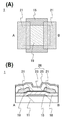
도 1의 (A) 및 도 1의 (B)는 트랜지스터의 일 형태를 설명하는 도면이다.
도 2의 (A) 내지 도 2의 (D)는 트랜지스터의 제작 방법의 일 형태를 설명하는 단면도이다.
도 3의 (A) 및 도 3의 (B)는 트랜지스터의 일 형태를 설명하는 도면이다.
도 4의 (A) 내지 도 4의 (D)는 트랜지스터의 제작 방법의 일 형태를 설명하는 단면도이다.
도 5는 트랜지스터의 일 형태를 설명하는 단면도이다.
도 6의 (A) 및 도 6의 (B)는 트랜지스터의 일 형태를 설명하는 도면이다.
도 7의 (A) 및 도 7의 (B)는 트랜지스터의 일 형태를 설명하는 도면이다.
도 8의 (A) 내지 도 8의 (C)는 표시 장치의 일 형태를 설명하는 상면도이다.
도 9의 (A) 및 도 9의 (B)는 표시 장치의 일 형태를 설명하는 단면도이다.
도 10은 표시 장치의 일 형태를 설명하는 단면도이다.
도 11의 (A) 내지 도 11의 (C)는 표시 장치의 일 형태를 설명하는 단면도이다.
도 12의 (A) 및 도 12의 (B)는 반도체 장치의 일 양태를 설명하는 도면이다.
도 13의 (A) 내지 도 13의 (C)는 전자기기를 설명하는 도면이다.
도 14의 (A) 내지 도 14의 (C)는 전자기기를 설명하는 도면이다.
도 15의 (A) 및 도 15의 (B)는 시료의 구조를 설명하는 도면이다.
도 16의 (A) 내지 도 16의 (C)는 TDS 분석 결과를 설명하는 도면이다.
도 17의 (A) 및 도 17의 (B)는 TDS 분석 결과를 설명하는 도면이다.
도 18의 (A) 및 도 18의 (B)는 TDS 분석 결과를 설명하는 도면이다.
도 19의 (A) 및 도 19의 (B)는 TDS 분석 결과를 설명하는 도면이다.
도 20의 (A) 내지 도 20의 (C)는 트랜지스터의 Vg-Id 특성을 설명하는 도면이다.
도 21의 (A) 내지 도 21의 (C)는 트랜지스터의 Vg-Id 특성을 설명하는 도면이다.
도 22의 (A) 내지 도 22의 (C)는 트랜지스터의 Vg-Id 특성을 설명하는 도면이다.
도 23은 질화 실리콘막의 수소 분자의 방출량 및 암모니아 분자의 방출량과 트랜지스터의 Vg-Id 특성을 설명하는 도면이다.1A and 1B are diagrams illustrating one embodiment of a transistor.
2A to 2D are cross-sectional views illustrating one embodiment of a method for manufacturing a transistor.
3A and 3B are diagrams illustrating one embodiment of a transistor.
4A to 4D are cross-sectional views illustrating one embodiment of a method for manufacturing a transistor.
5 is a cross-sectional view illustrating one embodiment of a transistor.
6A and 6B are diagrams illustrating one embodiment of a transistor.
7A and 7B are diagrams illustrating one embodiment of a transistor.
8A to 8C are top views illustrating one embodiment of the display device.
9A and 9B are cross-sectional views illustrating one embodiment of the display device.
10 is a cross-sectional view illustrating an embodiment of a display device.
11A to 11C are cross-sectional views illustrating one embodiment of a display device.
12A and 12B are views for explaining one embodiment of the semiconductor device.
13A to 13C are diagrams for explaining an electronic device.
14A to 14C are diagrams for explaining an electronic device.
15A and 15B are views for explaining the structure of a sample.
16A to 16C are diagrams illustrating the results of the TDS analysis.
17A and 17B are diagrams for explaining the TDS analysis results.
18A and 18B are diagrams illustrating the results of TDS analysis.
19A and 19B are diagrams illustrating the results of TDS analysis.
20A to 20C are diagrams illustrating the Vg-Id characteristics of the transistor.
21A to 21C are diagrams illustrating the Vg-Id characteristics of the transistor.
22A to 22C are diagrams for explaining the Vg-Id characteristics of the transistor.
Fig. 23 is a view for explaining the amount of hydrogen molecules released and the amount of ammonia released in the silicon nitride film and the Vg-Id characteristics of the transistor;
이하에서는, 본 발명의 실시형태에 대하여 도면을 이용하여 상세하게 설명한다. 단, 본 발명은 이하의 설명에 한정되는 것은 아니고, 본 발명의 취지 및 그 범위로부터 벗어나지 않고 그 형태 및 상세한 사항을 다양하게 변경할 수 있다는 것은, 당업자라면 용이하게 이해할 수 있을 것이다. 따라서, 본 발명은, 이하에 나타내는 실시형태 및 실시예의 기재 내용에 한정하여 해석되는 것은 아니다. 또한, 이하에 설명하는 실시형태 및 실시예에서, 동일 부분 또는 같은 기능을 갖는 부분에는, 동일한 부호 또는 동일한 해치 패턴을 다른 도면 간에 공통으로 이용하고, 그 반복 설명은 생략한다.EMBODIMENT OF THE INVENTION Hereinafter, embodiment of this invention is described in detail using drawing. However, the present invention is not limited to the following description, and it will be easily understood by those skilled in the art that various changes in form and details can be made without departing from the spirit and scope of the present invention. Therefore, this invention is not limited to description of embodiment and Example which are shown below. In addition, in the embodiment and the Example which are demonstrated below, the same code | symbol or the same hatch pattern is used in common among the other drawings in the same part or the part which has the same function, and the repeated description is abbreviate | omitted.
단, 본 명세서에서 설명하는 각 도면에서, 각 구성의 크기, 막의 두께, 또는 영역은 명료화를 위하여 과장되어 있는 경우가 있다. 따라서, 반드시 그 스케일로 한정되지 않는다.In each of the drawings described herein, however, the size, film thickness, or region of each component may be exaggerated for clarity. Therefore, it is not necessarily limited to the scale.
단, 본 명세서에서 이용하는 "제 1", "제 2", "제 3" 등의 용어는, 구성 요소의 혼동을 피하기 위하여 붙인 것이고, 수적으로 한정하는 것은 아니다. 따라서, 예를 들면, " 제 1"을 " 제 2" 또는 "제 3" 등과 적절히 치환하여 설명할 수 있다.However, the terms "first", "second", "third", etc. used in this specification are added in order to avoid confusion of components, and are not limited in number. Thus, for example, the description can be made by appropriately replacing "first" with "second" or "third" and the like.
"소스"나 "드레인"의 기능은 회로 동작에서 전류의 방향이 변화하는 경우 등에는 서로 바뀌는 경우가 있다. 따라서, 본 명세서에서는, "소스"나 "드레인"이라는 용어는 서로 치환하여 이용할 수 있는 것으로 한다.The functions of the "source" and the "drain" may change each other when the current direction changes in the circuit operation. Therefore, in this specification, the terms "source" and "drain" shall be used interchangeably.
단, 전압이란 2점간에서의 전위차를 말하고, 전위란 어느 일점에서의 정전장 중에 있는 단위 전하가 갖는 정전 에너지(전기적인 위치 에너지)를 말한다. 단, 일반적으로, 어느 일점에서의 전위와 기준이 되는 전위(예를 들면 접지 전위)와의 전위차를 단지 전위 혹은 전압이라고 부르고, 전위와 전압이 동의어로서 이용되는 경우가 많다. 따라서, 본 명세서에서는 특히 지정하는 경우를 제외하고, 전위를 전압이라고 바꾸어 읽어도 좋고, 전압을 전위라고 바꾸어 읽어도 좋은 것으로 한다.However, voltage means the potential difference between two points, and a potential means the electrostatic energy (electric potential energy) which the unit electric charge in the electrostatic field in any one point has. In general, however, the potential difference between the potential at any one point and the reference potential (for example, the ground potential) is simply called a potential or a voltage, and the potential and the voltage are often used as synonyms. Accordingly, in the present specification, except when specifically specified, the potential may be read as a voltage and the voltage may be read as a potential.
단, 산화물 반도체막을 포함하는 트랜지스터는 n채널형 트랜지스터이기 때문에; 따라서, 본 명세서에서, 게이트 전압이 0 V인 경우, 드레인 전류가 흐르지 않았다고 간주할 수 있는 트랜지스터를 노멀리 오프(normally-off) 특성을 갖는 트랜지스터라고 정의한다. 또한, 게이트 전압이 0 V인 경우, 드레인 전류가 흐르고 있다고 간주할 수 있는 트랜지스터를 노멀리 온(normally-on) 특성을 갖는 트랜지스터라고 정의한다.However, since the transistor including the oxide semiconductor film is an n-channel transistor; Therefore, in the present specification, when the gate voltage is 0 V, the transistor that can be considered that no drain current flows is defined as a transistor having a normally-off characteristic. In addition, when the gate voltage is 0 V, the transistor which can be regarded as the drain current is defined as a transistor having a normally-on characteristic.
(실시형태 1)(Embodiment 1)
본 실시형태에서는, 본 발명의 일 양태인 반도체 장치, 및 그 제작 방법에 대하여 도면을 참조하여 설명한다.In this embodiment, the semiconductor device which is one aspect of this invention, and its manufacturing method are demonstrated with reference to drawings.
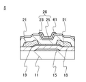
도 1의 (A) 및 도 1의 (B)는, 반도체 장치에 포함되는 트랜지스터(1)의 상면도 및 단면도이다. 도 1의 (A)는 트랜지스터(1)의 상면도이며, 도 1의 (B)는 도 1의 (A)의 일점 쇄선 A-B간의 단면도이다. 단, 도 1의 (A)에서는, 명료화를 위하여, 기판(11), 트랜지스터(1)의 구성 요소의 일부(예를 들면, 게이트 절연막(18)), 절연막(23), 질화 절연막(25) 등을 생략하였다.1A and 1B are top and cross-sectional views of the
도 1의 (A) 및 도 1의 (B)에 도시하는 트랜지스터(1)는, 기판(11) 위에 제공되는 게이트 전극(15)과, 기판(11) 및 게이트 전극(15) 위에 형성되는 게이트 절연막(18)과, 게이트 절연막(18)을 사이에 끼우고, 게이트 전극(15)과 중첩하는 산화물 반도체막(19)과, 산화물 반도체막(19)에 접촉하는 한쌍의 전극(21)을 포함한다. 또한, 게이트 절연막(18), 산화물 반도체막(19), 및 한쌍의 전극(21) 위에는, 절연막(23) 및 질화 절연막(25)을 포함하는 보호막(26)이 형성된다.The
본 실시형태에 나타내는 트랜지스터(1) 위에 제공되는 질화 절연막(25)은 승온 탈리 가스 분석법(TDS(Thermal Desorption Spectroscopy))으로, 수소 분자의 방출량이 5×10²¹ 분자/cm3 미만, 바람직하게는 3×10²¹ 분자/cm3 이하, 더욱 바람직하게는 1×10²¹ 분자/cm3 이하이며, 또한 암모니아 분자의 방출량이 1×10²² 분자/cm3 미만, 바람직하게는 5×10²¹ 분자/cm3 이하, 더욱 바람직하게는 1×10²¹ 분자/cm3 이하이다. 질화 절연막(25)으로부터 방출되는 수소 분자량 및 질소의 공급원인 암모니아 분자량이 적기 때문에; 따라서, 트랜지스터(1)에 포함되는 산화물 반도체막(19)으로의 수소 및 질소의 이동량이 적다.The
산화물 반도체막(19)에 포함되는 수소는, 금속 원자와 결합하는 산소와 반응하여 물이 됨과 동시에, 산소가 탈리한 격자(혹은 산소가 탈리한 부분)에는 결손이 형성되게 된다. 또한, 수소의 일부가 산소와 반응함으로써, 캐리어인 전자가 생긴다. 또한, 산화물 반도체막(19)에 포함되는 질소는 금속 원소 또는 산소와 반응함으로써, 캐리어인 전자가 생긴다. 이 결과, 산화물 반도체막(19)을 포함하는 트랜지스터는 노멀리 온 특성이 되기 쉽다. 따라서, 산화물 반도체막(19) 중의 수소 및 질소를 매우 줄임으로써, 문턱 전압의 마이너스 시프트를 억제할 수 있음과 동시에, 전기 특성의 편차를 저감시킬 수 있다. 또한, 트랜지스터의 소스 및 드레인에서의 누출 전류, 대표적으로는, 오프 전류를 저감시키는 것이 가능하다.Hydrogen contained in the
이 때문에, 트랜지스터(1) 위에, 승온 탈리 가스 분석법에 의해, 수소 분자의 방출량이 5×10²¹ 분자/cm3 미만, 바람직하게는 3×10²¹ 분자/cm3 이하, 더욱 바람직하게는 1×10²¹ 분자/cm3 이하이며, 또한 암모니아 분자의 방출량이 1×10²² 분자/cm3 미만, 바람직하게는 5×10²¹ 분자/cm3 이하, 더욱 바람직하게는 1×10²¹ 분자/cm3 이하인 질화 절연막을 제공함으로써, 질화 절연막으로부터 산화물 반도체막(19)으로의 수소 및 암모니아의 이동량이 적고, 산화물 반도체막(19) 중의 수소 및 질소의 농도를 저감시킬 수 있다. 또한, 트랜지스터(1) 위에는 질화 절연막(25)이 제공되어 있기 때문에; 따라서, 외부로부터 산화물 반도체막(19)으로의 물의 침입을 억제할 수 있다. 즉, 산화물 반도체막(19)으로의 물에 포함되는 수소의 침입을 억제할 수 있다. 이상의 결과, 문턱 전압의 마이너스 시프트를 억제할 수 있음과 동시에, 전기 특성의 편차를 저감시킬 수 있다. 또한, 트랜지스터의 소스 및 드레인에서의 누출 전류, 대표적으로는, 오프 전류를 저감시키는 것이 가능하다.For this reason, on the
질화 절연막(25)으로서는, 두께가 50 nm 이상 200 nm 이하의 질화 실리콘, 질화 산화 실리콘, 질화 알루미늄, 질화 산화 알루미늄 등을 이용할 수 있다. 단, 본 명세서에서, "산화 질화 실리콘막"이란, 그 조성으로서 질소보다 산소의 함유량이 많은 막을 가리키고, "질화 산화 실리콘막"이란, 그 조성으로서 산소보다 질소의 함유량이 많은 막을 가리킨다. 또한, "산화 질화 알루미늄막"이란, 그 조성으로서 질소보다 산소의 함유량이 많은 막을 가리키고, "질화 산화 알루미늄"막이란, 그 조성으로서 산소보다 질소의 함유량이 많은 막을 가리킨다.As the
여기서, 승온 탈리 가스 분석법(이하, TDS 분석이라고 함)에 의한, 수소 분자 및 암모니아 분자의 방출량의 측정 방법에 대하여, 이하에 설명한다.Here, the measuring method of the discharge amount of a hydrogen molecule and an ammonia molecule by a temperature-desorbing gas analysis method (henceforth TDS analysis) is demonstrated below.
TDS 분석에 의한 기체의 방출량은 스펙트럼의 적분치에 비례한다. 이 때문에, 절연막의 스펙트럼의 적분치와 표준 시료의 기준치에 대한 비에 의해, 기체의 방출량을 계산할 수 있다. 표준 시료의 기준치란, 소정의 원자를 포함한 시료의, 스펙트럼의 적분치에 대한 원자의 밀도의 비율이다.The amount of gas released by TDS analysis is proportional to the integral of the spectrum. For this reason, the emission amount of gas can be calculated by the ratio with respect to the integral value of the spectrum of an insulating film, and the reference value of a standard sample. The reference value of a standard sample is the ratio of the density of atoms to the integrated value of the spectrum of the sample containing a predetermined atom.
예를 들면, 표준 시료인 소정의 밀도의 수소를 포함한 실리콘 웨이퍼의 TDS 분석 결과, 및 절연막의 TDS 분석 결과로부터, 절연막의 수소 분자의 방출량(NH2)은 수학식 1로 구할 수 있다. 여기서, TDS 분석으로 얻어지는 질량수 2로 검출되는 스펙트럼 전부가 수소 분자 유래라고 가정한다. 또한, 질량수가 1 이외의 수소 원자의 동위체는 자연계에서의 존재 비율이 극미량이기 때문에 고려하지 않는다.For example, from the TDS analysis result of the silicon wafer containing hydrogen of predetermined density which is a standard sample, and the TDS analysis result of the insulating film, the emission amount N H2 of the hydrogen insulating film can be calculated | required by Formula (1). Here, it is assumed that all of the spectra detected by the
[수학식 1][Equation 1]

NH2는 수소 분자의 방출량이다. NH2(s)는 표준 시료로부터 탈리한 수소 분자를 밀도로 환산한 값이다. SH2(s)는 표준 시료를 TDS 분석했을 때의 스펙트럼의 적분치이다. 여기서, 표준 시료의 기준치를 NH2(s)/SH2(s)로 한다. SH2는 절연막을 TDS 분석했을 때의 스펙트럼의 적분치이다. α는 TDS 분석에서의 스펙트럼 강도에 영향을 주는 계수이다. 수학식 1의 상세한 사항에 관해서는, 일본국 특개평 6-275697 공보를 참조한다. 단, 상기 절연막의 수소 분자의 방출량은 전자 과학 주식회사(ESCO Ltd.)제의 승온 탈리 분석 장치 EMD-WA1000S/W를 이용하고, 표준 시료로서 1×10¹⁶ atoms/cm2의 수소 원자를 포함한 실리콘 웨이퍼를 이용하여 측정한다.N H2 is the amount of hydrogen molecules released. N H2 (s) is a value obtained by converting hydrogen molecules desorbed from a standard sample into density. S H2 (s) is the integral of the spectrum when the TDS analysis of the standard sample is performed. Here, the reference value of the standard sample is N H2 (s) / S H2 (s) . S H2 is the integral value of the spectrum when the insulating film is analyzed by TDS. α is a coefficient that affects the spectral intensity in the TDS analysis. For details of
또한, 상기 수학식 1에서, 절연막의 암모니아 분자의 방출량을 TDS 분석했을 때의 스펙트럼의 적분치를 SH2에 대입함으로써, 암모니아 분자의 방출량을 구할 수 있다.Further, by substituting in the equation (1), the integral value of the spectrum when the emission of ammonia molecules in the insulating film TDS analysis on SH 2, can be obtained a discharge amount of ammonia molecules.
이하에, 트랜지스터(1) 이외의 구성의 상세한 사항에 대하여 설명한다.Below, the details of the configuration other than the
기판(11)의 재질 등에 큰 제한은 없지만, 적어도, 후의 열처리에 견딜 수 있을 정도의 내열성을 가지고 있을 필요가 있다. 예를 들면, 유리 기판, 세라믹 기판, 석영 기판, 사파이어 기판 등을 기판(11)으로서 이용해도 좋다. 또한, 실리콘이나 탄화 실리콘 등의 단결정 반도체 기판, 다결정 반도체 기판, 실리콘 게르마늄 등의 화합물 반도체 기판, SOI(Silicon OnInsulator) 기판 등을 이용해도 좋다. 또한, 이러한 기판 위에 반도체 소자가 제공된 것을 기판(11)으로서 이용해도 좋다.Although there is no big restriction | limiting in the material of the board |
또한, 기판(11)으로서 가요성 기판을 이용하여, 가요성 기판 위에 직접 트랜지스터(1)를 제공해도 좋다. 또는, 기판(11)과 트랜지스터(1)의 사이에 박리층을 제공해도 좋다. 박리층은 그 위에 반도체 장치를 일부 혹은 전부 완성시킨 후, 기판(11)보다 분리하여, 다른 기판에 전재(轉載)하는데 이용할 수 있다. 그때, 트랜지스터(1)는 내열성이 낮은 기판이나 가요성의 기판에도 전재할 수 있다.As the
기판(11) 및 게이트 전극(15)의 사이에 하지 절연막을 제공해도 좋다. 하지 절연막으로서는, 산화 실리콘, 산화 질화 실리콘, 질화 실리콘, 질화 산화 실리콘, 산화 갈륨, 산화 하프늄, 산화 이트륨, 산화 알루미늄, 산화 질화 알루미늄 등이 있다. 단, 하지 절연막으로서 질화 실리콘, 산화 갈륨, 산화 하프늄, 산화 이트륨, 산화 알루미늄 등을 이용함으로써, 기판(11)으로부터 불순물, 대표적으로는 알칼리 금속, 물, 수소 등의 산화물 반도체막(19)으로의 확산을 억제할 수 있다.A base insulating film may be provided between the
게이트 전극(15)은 알루미늄, 크롬, 구리, 탄탈, 티탄, 몰리브덴, 텅스텐으로부터 선택된 금속 원소; 또는 상술한 금속 원소를 성분으로 하는 합금이나; 상술한 금속 원소를 조합한 합금; 등을 이용하여 형성할 수 있다. 또한, 망간, 지르코늄 중 어느 하나 또는 복수로부터 선택된 금속 원소를 이용해도 좋다. 또한, 게이트 전극(15)은, 단층 구조로 해도, 2층 이상의 적층 구조로 해도 좋다. 예를 들면, 실리콘을 포함한 알루미늄막의 단층 구조; 알루미늄막 위에 티탄막을 적층하는 2층 구조; 질화 티탄막 위에 티탄막을 적층하는 2층 구조; 질화 티탄막 위에 텅스텐막을 적층하는 2층 구조; 질화 탄탈막 또는 질화 텅스텐막 위에 텅스텐막을 적층하는 2층 구조; 티탄막과 그 티탄막 위에 알루미늄막을 적층하고, 또한, 그 위에 티탄막을 형성하는 3층 구조 등이 있다. 또한, 알루미늄을 포함하고, 티탄, 탄탈, 텅스텐, 몰리브덴, 크롬, 네오디뮴, 스칸듐으로부터 선택된 원소의 막, 또는 복수 조합한 합금막, 혹은 질화막을 이용해도 좋다.The
게이트 전극(15)은, 인듐 주석 산화물, 산화 텅스텐을 포함한 인듐 산화물, 산화 텅스텐을 포함한 인듐 아연 산화물, 산화 티탄을 포함한 인듐 산화물, 산화 티탄을 포함한 인듐 주석 산화물, 인듐 아연 산화물, 산화 실리콘을 포함한 인듐 주석 산화물 등의 투광성을 갖는 도전성 재료를 이용하여 형성될 수 있다. 또한, 상기 투광성을 갖는 도전성 재료와 상기 금속 원소를 이용하여 형성된 적층 구조를 가질 수도 있다.The
또한, 게이트 전극(15)과 게이트 절연막(18)과의 사이에, In-Ga-Zn계 산질화물 반도체막, In-Sn계 산질화물 반도체막, In-Ga계 산질화물 반도체막, In-Zn계 산질화물 반도체막, Sn계 산질화물 반도체막, In계 산질화물 반도체막, 금속 질화막(InN, ZnN 등) 등을 제공해도 좋다. 이러한 막은 5 eV 이상, 바람직하게는 5.5 eV 이상의 일 함수를 갖고, 산화물 반도체의 전자 친화력보다 큰 값이기 때문에; 따라서, 산화물 반도체를 포함한 트랜지스터의 문턱 전압을 플러스로 시프트할 수 있다. 따라서, 소위 노멀리 오프 특성의 스위칭 소자를 얻을 수 있다. 예를 들면, In-Ga-Zn계 산질화물 반도체막을 이용하는 경우, 적어도 산화물 반도체막(19)보다 높은 질소 농도, 구체적으로는 7 원자% 이상의 In-Ga-Zn계 산질화물 반도체막을 이용한다.In-Ga-Zn-based oxynitride semiconductor film, In-Sn-based oxynitride semiconductor film, In-Ga-based oxynitride semiconductor film, In-Zn between the
게이트 절연막(18)은 예를 들면 산화 실리콘, 산화 질화 실리콘, 질화 산화 실리콘, 질화 실리콘, 산화 알루미늄, 산화 하프늄, 산화 갈륨 또는 Ga-Zn계 금속 산화물 등을 이용하면 좋고, 적층 또는 단층으로 형성한다. 단, 산화물 반도체막(19)과의 계면 특성을 향상시키기 위해, 게이트 절연막(18)에서 적어도 산화물 반도체막(19)과 접촉하는 영역은 산화 절연막으로 형성하는 것이 바람직하다.The
게이트 절연막(18)에, 산소, 수소, 물 등의 블로킹 효과를 갖는 절연막을 제공함으로써, 산화물 반도체막(19)으로부터의 산소의 외부로의 확산과, 외부로부터 산화물 반도체막(19)에의 수소, 물 등의 침입을 막을 수 있다. 산소, 수소, 물 등의 블로킹 효과를 갖는 절연막으로서는, 산화 알루미늄, 산화 질화 알루미늄, 산화 갈륨, 산화 질화 갈륨, 산화 이트륨, 산화 질화 이트륨, 산화 하프늄, 산화 질화 하프늄 등이 있다.By providing the
또한, 게이트 절연막(18)을 적층 구조로 하고, 제 1 질화 실리콘막으로서 결함이 적은 질화 실리콘막으로 하고, 제 1 질화 실리콘막 위에, 질화 절연막(25)과 같이, 수소 분자 방출량 및 암모니아 분자 방출량이 적은 질화 실리콘막을 제 2 질화 실리콘막을 형성하여, 제 2 질화 실리콘막 위에 산화 절연막을 형성함으로써, 게이트 절연막(18)으로서 결함이 적고, 또한 수소 분자 및 암모니아 분자의 방출량이 적은 게이트 절연막을 형성할 수 있다. 이 결과, 게이트 절연막(18)에 포함되는 수소 및 질소가 산화물 반도체막(19)으로 이동하는 것을 억제할 수 있다.In addition, the
게이트 절연막(18)으로서 질화 실리콘막을 이용함으로써, 이하의 효과를 얻을 수 있다. 질화 실리콘막은 산화 실리콘막과 비교하여 비유전률이 높고, 동등한 정전 용량을 얻는데 큰 막두께가 필요하다. 따라서, 게이트 절연막을 물리적으로 두껍게 할 수 있다. 따라서, 트랜지스터(1)의 절연 내압의 저하를 억제하고, 절연 내압을 향상시켜, 반도체 장치의 정전 파괴를 억제할 수 있다.By using a silicon nitride film as the
또한, 게이트 전극(15)으로서 구리를 이용하여 게이트 전극(15)에 접촉하는 게이트 절연막(18)으로서 질화 실리콘막을 이용하는 경우, 가열에 의한 암모니아 분자 방출량을 가능한 한 저감시키는 질화 실리콘막을 이용하는 것이 바람직하다. 따라서, 상기 질화 실리콘막으로서 질화 절연막(25)에 적용할 수 있는 질화 실리콘막을 이용할 수 있다. 이 결과, 구리와 암모니아 분자가 반응하는 것을 억제할 수 있다.In addition, when using the silicon nitride film as the
산화물 반도체를 이용한 트랜지스터에서, 산화물 반도체막 및 게이트 절연막의 계면 또는 게이트 절연막 중에 포획 준위(계면 준위라고도 함)가 있으면, 트랜지스터의 문턱 전압의 변동, 대표적으로는, 문턱 전압의 마이너스 시프트, 및 트랜지스터가 온 상태가 될 때 드레인 전류가 1 자리수 변화하는데 필요한 게이트 전압을 나타내는 서브 문턱 계수(S값)의 증대의 원인이 된다. 이 결과, 트랜지스터마다 전기 특성이 변동된다는 문제가 있다. 따라서, 게이트 절연막으로서 결함이 적은 질화 실리콘막을 이용함으로써, 문턱 전압의 마이너스 시프트, 및 트랜지스터의 전기 특성의 편차를 저감시킬 수 있다.In a transistor using an oxide semiconductor, if there is a capture level (also referred to as a interface level) in the interface between the oxide semiconductor film and the gate insulating film or in the gate insulating film, a variation in the threshold voltage of the transistor, typically a negative shift in the threshold voltage, and a transistor When turned on, it causes the increase of the sub-threshold coefficient (S value) indicating the gate voltage required for the drain current to change by one digit. As a result, there is a problem that the electrical characteristics vary from transistor to transistor. Therefore, by using the silicon nitride film with few defects as the gate insulating film, the negative shift of the threshold voltage and the variation of the electrical characteristics of the transistor can be reduced.
게이트 절연막(18)은 하프늄 실리케이트(HfSiOx), 질소가 첨가된 하프늄 실리케이트(HfSixOyNz), 질소가 첨가된 하프늄 알루미네이트(HfAlxOyNz), 산화 하프늄, 산화 이트륨 등의 high-k 재료를 이용하여 형성됨으로써, 트랜지스터의 게이트 누출을 저감시킬 수 있다.The
게이트 절연막(18)의 두께는 5 nm 이상 400 nm 이하, 보다 바람직하게는 10 nm 이상 300 nm 이하, 보다 바람직하게는 50 nm 이상 250 nm 이하로 하면 좋다.The thickness of the
산화물 반도체막(19)은 적어도 인듐(In) 혹은 아연(Zn)을 포함하는 것이 바람직하다. 또는, In과 Zn의 쌍방을 포함하는 것이 바람직하다. 또한, 이 산화물 반도체막을 포함한 트랜지스터의 전기 특성의 편차를 줄이기 위하여, 그것들과 함께, 스태빌라이저를 하나 또는 복수 갖는 것이 바람직하다.The
스태빌라이저로서는, 갈륨(Ga), 주석(Sn), 하프늄(Hf), 알루미늄(Al), 또는 지르코늄(Zr) 등이 있다. 다른 스태빌라이저로서는, 란타노이드인, 란탄(La), 세륨(Ce), 프라세오디뮴(Pr), 네오디뮴(Nd), 사마륨(Sm), 유로퓸(Eu), 가돌리늄(Gd), 테르븀(Tb), 디스프로슘(Dy), 홀뮴(Ho), 에르븀(Er), 툴륨(Tm), 이테르븀(Yb), 루테튬(Lu) 등이 있다.Examples of the stabilizer include gallium (Ga), tin (Sn), hafnium (Hf), aluminum (Al), zirconium (Zr), and the like. Other stabilizers include lanthanides, lanthanum (La), cerium (Ce), praseodymium (Pr), neodymium (Nd), samarium (Sm), europium (Eu), gadolinium (Gd), terbium (Tb), and dysprosium ( Dy), holmium (Ho), erbium (Er), thulium (Tm), ytterbium (Yb), lutetium (Lu), and the like.
예를 들면, 산화물 반도체로서, 다음의 것들이 이용될 수 있다: 산화 인듐, 산화 주석, 산화 아연; 2원계 금속 산화물인 In-Zn계 금속 산화물, Sn-Zn계 금속 산화물, Al-Zn계 금속 산화물, Zn-Mg계 금속 산화물, Sn-Mg계 금속 산화물, In-Mg계 금속 산화물, In-Ga계 금속 산화물, In-W계 금속 산화물; 3원계 금속 산화물인 In-Ga-Zn계 금속 산화물(IGZO라고도 표기함), In-Al-Zn계 금속 산화물, In-Sn-Zn계 금속 산화물, Sn-Ga-Zn계 금속 산화물, Al-Ga-Zn계 금속 산화물, Sn-Al-Zn계 금속 산화물, In-Hf-Zn계 금속 산화물, In-La-Zn계 금속 산화물, In-Ce-Zn계 금속 산화물, In-Pr-Zn계 금속 산화물, In-Nd-Zn계 금속 산화물, In-Sm-Zn계 금속 산화물, In-Eu-Zn계 금속 산화물, In-Gd-Zn계 금속 산화물, In-Tb-Zn계 금속 산화물, In-Dy-Zn계 금속 산화물, In-Ho-Zn계 금속 산화물, In-Er-Zn계 금속 산화물, In-Tm-Zn계 금속 산화물, In-Yb-Zn계 금속 산화물, In-Lu-Zn계 금속 산화물; 4원계 금속 산화물인 In-Sn-Ga-Zn계 금속 산화물, In-Hf-Ga-Zn계 금속 산화물, In-Al-Ga-Zn계 금속 산화물, In-Sn-Al-Zn계 금속 산화물, In-Sn-Hf-Zn계 금속 산화물, In-Hf-Al-Zn계 금속 산화물을 이용할 수 있다.For example, as the oxide semiconductor, the following may be used: indium oxide, tin oxide, zinc oxide; In-Zn-based metal oxides, Sn-Zn-based metal oxides, Al-Zn-based metal oxides, Zn-Mg-based metal oxides, Sn-Mg-based metal oxides, In-Mg-based metal oxides, and In-Ga as binary metal oxides Metal oxides and In-W metal oxides; In-Ga-Zn-based metal oxides (also referred to as IGZOs), In-Al-Zn-based metal oxides, In-Sn-Zn-based metal oxides, Sn-Ga-Zn-based metal oxides, and Al-Ga ternary metal oxides -Zn-based metal oxides, Sn-Al-Zn-based metal oxides, In-Hf-Zn-based metal oxides, In-La-Zn-based metal oxides, In-Ce-Zn-based metal oxides, In-Pr-Zn-based metal oxides , In-Nd-Zn-based metal oxide, In-Sm-Zn-based metal oxide, In-Eu-Zn-based metal oxide, In-Gd-Zn-based metal oxide, In-Tb-Zn-based metal oxide, In-Dy- Zn-based metal oxides, In-Ho-Zn-based metal oxides, In-Er-Zn-based metal oxides, In-Tm-Zn-based metal oxides, In-Yb-Zn-based metal oxides, and In-Lu-Zn-based metal oxides; In-Sn-Ga-Zn-based metal oxides which are quaternary metal oxides, In-Hf-Ga-Zn-based metal oxides, In-Al-Ga-Zn-based metal oxides, In-Sn-Al-Zn-based metal oxides, In -Sn-Hf-Zn-based metal oxides and In-Hf-Al-Zn-based metal oxides can be used.
단, 여기서, 예를 들면, In-Ga-Zn계 금속 산화물이란, In과 Ga와 Zn을 주성분으로서 갖는 산화물이라는 의미이며, In과 Ga와 Zn의 비율은 묻지 않는다. 또한, In과 Ga와 Zn 이외의 금속 원소가 포함되어 있어도 좋다.Here, for example, an In—Ga—Zn-based metal oxide means an oxide having In, Ga, and Zn as main components, and the ratio of In, Ga, and Zn does not matter. Moreover, metal elements other than In, Ga, and Zn may be contained.
또한, 산화물 반도체로서 InMO3(ZnO)m(m>0이고, m은 정수가 아님)로 표기되는 재료를 이용해도 좋다. 단, M은 Ga, Fe, Mn, 및 Co로부터 선택된 하나의 금속 원소 또는 복수의 금속 원소를 나타낸다. 또한, 산화물 반도체로서 In2SnO5(ZnO)n(n>0이고, n은 정수)로 표기되는 재료를 이용해도 좋다.As the oxide semiconductor, a material represented by InMO 3 (ZnO) m (m> 0 and m is not an integer) may be used. Provided that M represents one metal element or a plurality of metal elements selected from Ga, Fe, Mn, and Co. As the oxide semiconductor, a material represented by In 2 SnO 5 (ZnO) n (n> 0 and n is an integer) may be used.
예를 들면, In:Ga:Zn = 1:1:1( = 1/3:1/3:1/3), In:Ga:Zn = 2:2:1( = 2/5:2/5:1/5), 혹은 In:Ga:Zn = 3:1:2( = 1/2:1/6:1/3)의 원자수비의 In-Ga-Zn계 금속 산화물이나 그 조성의 근방의 산화물을 이용할 수 있다. 혹은, In:Sn:Zn = 1:1:1( = 1/3:1/3:1/3), In:Sn:Zn = 2:1:3( = 1/3:1/6:1/2) 혹은 In:Sn:Zn = 2:1:5( = 1/4:1/8:5/8)의 원자수비의 In-Sn-Zn계 금속 산화물을 이용하면 좋다. 또한, 금속 산화물의 원자수비는 오차로서 상기의 원자수비의 ±20%의 변동을 포함한다.For example, In: Ga: Zn = 1: 1: 1 (= 1/3: 1/3: 1/3), In: Ga: Zn = 2: 2: 1 (= 2/5: 2/5 : 1/5) or In: Ga: Zn = 3: 1: 2 (= 1/2: 1/6: 1/3) in atomic ratio of In-Ga-Zn-based metal oxide and its composition Oxides can be used. Or In: Sn: Zn = 1: 1: 1 (= 1/3: 1/3: 1/3), In: Sn: Zn = 2: 1 (3: 1/3: 1/16: 1) / 2) or an In-Sn-Zn metal oxide having an atomic ratio of In: Sn: Zn = 2: 1: 5 (= 1/4: 1/8: 5/8). In addition, the atomic ratio of the metal oxide includes a variation of ± 20% of the atomic ratio as an error.
그러나, 이것들에 한정되지 않고, 필요로 하는 반도체 특성 및 전기 특성(전계 효과 이동도, 문턱 전압, 편차 등)에 따라 적절한 조성의 것을 이용하면 좋다. 필요로 하는 반도체 특성을 얻기 위해, 캐리어 밀도나 불순물 농도, 결함 밀도, 금속 원소와 산소의 원자수비, 원자간 거리, 밀도 등을 적절한 것으로 하는 것이 바람직하다.However, the present invention is not limited to these, and those having an appropriate composition may be used according to required semiconductor characteristics and electrical characteristics (field effect mobility, threshold voltage, deviation, and the like). In order to obtain the required semiconductor characteristics, it is preferable to appropriately set the carrier density, the impurity concentration, the defect density, the atomic ratio of the metal element and oxygen, the interatomic distance, the density, and the like.
예를 들면, In-Sn-Zn계 금속 산화물을 이용하는 경우에서는 비교적 용이하게 높은 이동도를 얻을 수 있다. 그러나, In-Ga-Zn계 금속 산화물을 이용하는 경우에서도, 벌크 내 결함 밀도를 낮게 함으로써 이동도를 높일 수 있다.For example, when In-Sn-Zn-based metal oxides are used, high mobility can be obtained relatively easily. However, even when In-Ga-Zn-based metal oxides are used, mobility can be increased by lowering the defect density in the bulk.
단, 산화물 반도체막(19)을 형성할 수 있는 금속 산화물은 에너지 갭이 2 eV 이상, 바람직하게는 2.5 eV 이상, 보다 바람직하게는 3 eV 이상이다. 이와 같이, 에너지 갭이 넓은 산화물 반도체를 이용함으로써, 트랜지스터의 오프 전류를 저감시킬 수 있다.However, the metal oxide capable of forming the
단, 산화물 반도체막(19)은 비정질 구조, 단결정 구조, 또는 다결정 구조여도 좋다.However, the
산화물 반도체막(19)으로서 결정부를 갖는 CAAC-OS(C Axis Aligned Crystalline Oxide Semiconductor라고도 함)막을 이용해도 좋다.As the
CAAC-OS막은 복수의 결정부를 포함하는 산화물 반도체막의 하나이며, 대부분의 결정부는 한 변이 100 nm 미만의 입방체 내에 들어가는 크기이다. 따라서, CAAC-OS막에 포함되는 결정부는 한 변이 10 nm 미만, 5 nm 미만 또는 3 nm 미만의 입방체 내에 들어가는 크기의 경우도 포함된다. CAAC-OS막은 미결정 산화물 반도체막보다 결함 준위 밀도가 낮다는 특징이 있다. 이하, CAAC-OS막에 대하여 상세한 설명을 행한다.The CAAC-OS film is one of oxide semiconductor films including a plurality of crystal parts, and most of the crystal parts have a size that one side enters a cube of less than 100 nm. Therefore, the crystal part contained in a CAAC-OS film also includes the case where the size | side which one side enters in a cube of less than 10 nm, less than 5 nm, or less than 3 nm. The CAAC-OS film has a feature that the density of defect states is lower than that of the microcrystalline oxide semiconductor film. Hereinafter, the CAAC-OS film will be described in detail.
CAAC-OS막을 투과형 전자 현미경(TEM:Transmission Electron Microscope)에 의해 관찰하면, 결정부들 간의 명확한 경계, 즉 결정립계(그레인 바운더리라고도 함)를 확인할 수 없다. 따라서, CAAC-OS막은 결정립계에 기인한 전자 이동도의 저하가 일어나기 어렵다고 할 수 있다.When the CAAC-OS film was observed by a transmission electron microscope (TEM), a clear boundary between crystal parts, that is, grain boundaries (also called grain boundaries) could not be confirmed. Therefore, it can be said that the CAAC-OS film is less likely to lower the electron mobility due to the grain boundary.
CAAC-OS막을 시료면과 대략 평행한 방향으로부터 TEM에 의해 관찰(단면 TEM 관찰)하면, 결정부에서, 금속 원자가 층상으로 배열되어 있는 것을 확인할 수 있다. 금속 원자의 각 층은 CAAC-OS막의 막을 형성하는 면(피형성면이라고도 함) 또는 상면의 요철을 반영한 형상이며, CAAC-OS막의 피형성면 또는 상면과 평행하게 배열한다.When the CAAC-OS film was observed by TEM from a direction substantially parallel to the sample surface (cross section TEM observation), it can be confirmed that the metal atoms are arranged in a layer in the crystal part. Each layer of the metal atom is a shape reflecting the surface (also referred to as a to-be-formed surface) or the uneven surface of the CAAC-OS film that forms the film, and is arranged in parallel with the to-be-formed surface or the upper surface of the CAAC-OS film.
한편, CAAC-OS막을 시료면과 대략 수직인 방향으로부터 TEM에 의해 관찰(평면 TEM 관찰)하면, 결정부에서, 금속 원자가 삼각 형상 또는 육각 형상으로 배열되어 있는 것을 확인할 수 있다. 그러나, 다른 결정부간에서, 금속 원자의 배열에 규칙성은 볼 수 없다.On the other hand, when the CAAC-OS film is observed by TEM (planar TEM observation) from a direction substantially perpendicular to the sample surface, it can be confirmed that the metal atoms are arranged in a triangular shape or a hexagonal shape in the crystal part. However, between different crystal regions, no regularity is seen in the arrangement of the metal atoms.
단면 TEM 관찰 및 평면 TEM 관찰로부터, CAAC-OS막의 결정부는 배향성을 가지고 있는 것을 알 수 있다.From the cross-sectional TEM observation and the planar TEM observation, it can be seen that the crystal part of the CAAC-OS film has orientation.
CAAC-OS막에 대하여, X선 회절(XRD:X-Ray Diffraction) 장치를 이용하여 구조 해석을 행한다. 예를 들면 InGaZnO4의 결정을 포함하는 CAAC-OS막의 out-of-plane법에 의한 해석에서는, 회절각(2θ)이 31° 근방에 피크가 나타나는 경우가 있다. 이 피크는 InGaZnO4의 결정의 (009)면에 귀속되기 때문에, CAAC-OS막의 결정이 c축 배향성을 갖고, c축이 피형성면 또는 상면에 대략 수직인 방향을 향하고 있는 것을 확인할 수 있다.The CAAC-OS film is subjected to structural analysis using an X-ray diffraction (XRD: X-Ray Diffraction) apparatus. For example, in the analysis by the out-of-plane method of the CAAC-OS film containing the InGaZnO 4 crystal, a peak may appear in the vicinity of the diffraction angle 2θ at 31 °. Since this peak belongs to the (009) plane of the InGaZnO 4 crystal, it can be confirmed that the crystal of the CAAC-OS film has the c-axis orientation, and the c-axis is directed in a direction substantially perpendicular to the formation surface or the upper surface.
한편, CAAC-OS막에 대하여, c축에 대략 수직인 방향으로부터 X선을 입사시키는 in-plane법에 의한 해석에서는, 2θ가 56° 근방에 피크가 나타나는 경우가 있다. 이 피크는 InGaZnO4의 결정의 (110)면에 귀속된다. InGaZnO4의 단결정 산화물 반도체막의 경우, 2θ를 56° 근방에 고정하고, 시료면의 법선 벡터를 축(φ축)으로 하여 시료를 회전시키면서 분석(φ스캔)을 행한다. 시료가 InGaZnO4의 단결정 산화물 반도체막인 경우, (110)면과 등가인 결정면에 귀속되는 피크가 6개 관찰된다. 이것에 비해, CAAC-OS막의 경우는 2θ를 56° 근방에 고정하여 φ스캔한 경우에도 명료한 피크가 나타나지 않는다.On the other hand, in the analysis by the in-plane method in which X-rays are incident from the direction substantially perpendicular to the c-axis with respect to the CAAC-OS film, a peak may appear near 56 ° in 2θ. This peak belongs to the (110) plane of the InGaZnO 4 crystal. In the case of the InGaZnO 4 single crystal oxide semiconductor film, 2θ is fixed near 56 °, and the analysis (φ scan) is performed while rotating the sample with the normal vector of the sample surface as the axis (φ axis). When the sample is an InGaZnO 4 single crystal oxide semiconductor film, six peaks belonging to the crystal plane equivalent to the (110) plane are observed. In contrast, in the case of the CAAC-OS film, no clear peak appears even when 2θ is fixed at around 56 ° and φ scans.
이상으로부터, CAAC-OS막에서는 다른 결정부간에서는 a축 및 b축의 배향은 불규칙하지만, c축 배향성을 갖고, 또한 c축이 피형성면 또는 상면의 법선 벡터에 평행한 방향을 향하고 있는 것을 알 수 있다. 따라서, 상술한 단면 TEM 관찰로 확인된 층상으로 배열된 금속 원자의 각 층은 결정의 ab면에 평행한 면이다.As mentioned above, although the orientation of a-axis and b-axis is irregular between different crystal parts in CAAC-OS film | membrane, it has a c-axis orientation, and it turns out that a c-axis faces a direction parallel to the normal vector of a to-be-formed surface or an upper surface. have. Therefore, each layer of the metal atoms arranged in the layer form identified by the above-described cross-sectional TEM observation is a plane parallel to the ab plane of the crystal.
단, 결정부는 CAAC-OS막을 성막했을 때, 또는 가열 처리 등의 결정화 처리를 행했을 때에 형성된다. 상술한 바와 같이, 결정의 c축은 CAAC-OS막의 피형성면 또는 상면의 법선 벡터에 평행한 방향으로 배향한다. 따라서, 예를 들면, CAAC-OS막의 형상을 에칭 등에 의해 변화시킨 경우, 결정의 c축이 CAAC-OS막의 피형성면 또는 상면의 법선 벡터와 평행하게 되지 않는 경우도 있다.However, the crystal part is formed when the CAAC-OS film is formed or when crystallization such as heat treatment is performed. As described above, the c-axis of the crystal is oriented in a direction parallel to the normal vector of the formed surface or the upper surface of the CAAC-OS film. Therefore, for example, when the shape of the CAAC-OS film is changed by etching or the like, the c-axis of the crystal may not be parallel to the normal vector of the formed surface or the upper surface of the CAAC-OS film.
또한, CAAC-OS막 중의 결정화도가 균일하지 않아도 좋다. 예를 들면, CAAC-OS막의 결정부가 CAAC-OS막의 상면 근방으로부터의 결정 성장에 의해 형성되는 경우, 상면 근방의 영역은 피형성면 근방의 영역보다 결정화도가 높아지는 경우가 있다. 또한, CAAC-OS막에 불순물을 첨가하는 경우, 불순물이 첨가된 영역의 결정화도가 변화되어, 부분적으로 결정화도가 다른 영역이 형성되는 경우도 있다.In addition, the crystallinity in the CAAC-OS film may not be uniform. For example, when the crystal part of the CAAC-OS film is formed by crystal growth from the vicinity of the upper surface of the CAAC-OS film, the region near the upper surface may have a higher degree of crystallinity than the region near the formation surface. In addition, in the case where an impurity is added to the CAAC-OS film, the crystallinity of the region where the impurity is added changes, so that a region having a different degree of crystallinity may be formed in some cases.
단, InGaZnO4의 결정을 갖는 CAAC-OS막의 out-of-plane법에 의한 해석에서는 2θ가 31° 근방의 피크 외에, 2θ가 36° 근방에도 피크가 나타나는 경우가 있다. 2θ가 36° 근방의 피크는 CAAC-OS막 중의 일부에 c축 배향성을 갖지 않는 결정이 포함되는 것을 나타낸다. CAAC-OS막은 2θ가 31° 근방에 피크를 나타내고, 2θ가 36° 근방에 피크를 나타내지 않는 것이 바람직하다.However, in the analysis by the out-of-plane method of the CAAC-OS film having the InGaZnO 4 crystal, in addition to the peak at 2θ of around 31 °, the peak may also appear at 2θ of 36 °. The peak of 2θ near 36 ° indicates that some of the CAAC-OS films contain crystals having no c-axis orientation. In the CAAC-OS film, it is preferable that 2θ shows a peak near 31 ° and 2θ does not show a peak near 36 °.
CAAC-OS막을 이용한 트랜지스터는 가시광이나 자외광의 조사에 의한 전기 특성의 변동이 작다. 따라서, 상기 트랜지스터는 신뢰성이 높다.The transistor using the CAAC-OS film has a small variation in electrical characteristics due to irradiation with visible or ultraviolet light. Thus, the transistor is highly reliable.
또한, 산화물 반도체막(19)은 복수의 산화물 반도체막이 적층된 구조여도 좋다. 예를 들면, 산화물 반도체막(19)을 제 1 산화물 반도체막과 제 2 산화물 반도체막의 적층으로 하고, 제 1 산화물 반도체막과 제 2 산화물 반도체막에 다른 조성의 금속 산화물을 이용해도 좋다. 예를 들면, 제 1 산화물 반도체막에 2원계 금속 산화물 내지 4원계 금속 산화물의 하나를 이용하고, 제 2 산화물 반도체막에 제 1 산화물 반도체막과 다른 2원계 금속 산화물 내지 4원계 금속 산화물을 이용해도 좋다.The
또한, 제 1 산화물 반도체막과 제 2 산화물 반도체막의 구성 원소를 동일하게 하고, 양자의 조성을 다르게 해도 좋다. 예를 들면, 제 1 산화물 반도체막의 원자수비를 In:Ga:Zn = 3:1:2로 하고, 제 2 산화물 반도체막의 원자수비를 In:Ga:Zn = 1:1:1로 해도 좋다. 또한, 제 1 산화물 반도체막의 원자수비를 In:Ga:Zn = 2:1:3으로 하고, 제 2 산화물 반도체막의 원자수비를 In:Ga:Zn = 1:3:2로 해도 좋다. 단, 각 산화물 반도체막의 원자수비는 오차로서 상기의 원자수비의 ±20%의 변동을 포함한다.In addition, the constituent elements of the first oxide semiconductor film and the second oxide semiconductor film may be the same, and the composition of the both may be different. For example, the atomic ratio of the first oxide semiconductor film may be In: Ga: Zn = 3: 1: 1, and the atomic ratio of the second oxide semiconductor film may be In: Ga: Zn = 1: 1: 1. The atomic ratio of the first oxide semiconductor film may be In: Ga: Zn = 2: 1: 3, and the atomic ratio of the second oxide semiconductor film may be In: Ga: Zn = 1: 3: 2. However, the atomic ratio of each oxide semiconductor film contains a variation of ± 20% of the atomic ratio as an error.
이 때, 제 1 산화물 반도체막과 제 2 산화물 반도체막 중, 게이트 전극에 가까운 쪽(채널측)의 산화물 반도체막의 In과 Ga의 함유율을 In>Ga로 하면 좋다. 또 게이트 전극으로부터 먼 쪽(백 채널측)의 산화물 반도체막의 In과 Ga의 함유율을 In≤Ga로 하면 좋다.In this case, the content of In and Ga in the oxide semiconductor film on the side closer to the gate electrode (channel side) among the first oxide semiconductor film and the second oxide semiconductor film may be set to In> Ga. In addition, the content ratio of In and Ga of the oxide semiconductor film on the side (back channel side) far from the gate electrode may be In ≦ Ga.
또한, 산화물 반도체막(19)을 3층 구조로 하고, 제 1 산화물 반도체막∼제 3 산화물 반도체막의 구성 원소를 동일하게 하고, 또한 각각의 조성을 다르게 해도 좋다. 예를 들면, 제 1 산화물 반도체막의 원자수비를 In:Ga:Zn = 1:3:2로 하고, 제 2 산화물 반도체막의 원자수비를 In:Ga:Zn = 3:1:2로 하고, 제 3 산화물 반도체막의 원자수비를 In:Ga:Zn = 1:1:1로 해도 좋다.In addition, the
Ga 및 Zn보다 In의 원자수비가 작은 산화물 반도체막, 대표적으로는 원자수비가 In:Ga:Zn = 1:3:2인 제 1 산화물 반도체막은, Ga 및 Zn보다 In의 원자수비가 큰 산화물 반도체막, 대표적으로는, 제 2 산화물 반도체막, 및 Ga, Zn, 및 In의 원자수비가 같은 산화물 반도체막, 대표적으로는 제 3 산화물 반도체막과 비교하여, 산소 결손이 생기기 어렵기 때문에, 캐리어 밀도가 증가하는 것을 억제할 수 있다. 또한, 원자수비가 In:Ga:Zn = 1:3:2인 제 1 산화물 반도체막이 비정질 구조라면, 제 2 산화물 반도체막이 CAAC-OS막이 되기 쉽다.An oxide semiconductor film having a smaller atomic ratio of In than Ga and Zn, typically a first oxide semiconductor film having an atomic ratio of In: Ga: Zn = 1: 1: 2 is an oxide semiconductor having a larger atomic ratio of In than Ga and Zn. Since the film, typically, the second oxide semiconductor film, and the oxide semiconductor film having the same atomic ratio of Ga, Zn, and In, and typically the third oxide semiconductor film, oxygen deficiency is less likely to occur, carrier density Can be suppressed from increasing. If the first oxide semiconductor film having an atomic number ratio of In: Ga: Zn = 1: 1: 2 is an amorphous structure, the second oxide semiconductor film is likely to be a CAAC-OS film.
제 1 산화물 반도체막∼제 3 산화물 반도체막의 구성 원소는 동일하기 때문에, 제 1 산화물 반도체막은 제 2 산화물 반도체막과의 계면에서의 트랩 준위가 적다. 따라서, 산화물 반도체막(19)을 상기 구조로 함으로써, 트랜지스터의 경시 변화나 광 BT 스트레스 시험에 의한 문턱 전압의 변동량을 저감시킬 수 있다.Since the constituent elements of the first oxide semiconductor film to the third oxide semiconductor film are the same, the first oxide semiconductor film has little trap level at the interface with the second oxide semiconductor film. Therefore, by making the
산화물 반도체에서는 주로 중금속의 s궤도가 캐리어 전도에 기여하고 있고, In의 함유율을 많이 함으로써, 보다 많은 s궤도가 중첩된다. 따라서, In>Ga의 조성이 되는 산화물은 In≤Ga의 조성이 되는 산화물과 비교하여 높은 캐리어 이동도를 구비한다. 또한, Ga는 In과 비교하여 산소 결손의 형성 에너지가 크고 산소 결손이 생기기 어렵기 때문에; In≤Ga의 조성이 되는 산화물은 In>Ga의 조성이 되는 산화물과 비교하여 안정된 특성을 구비한다.In oxide semiconductors, the s orbits of heavy metals mainly contribute to carrier conduction, and by increasing the content of In, more s orbits overlap. Accordingly, the oxide having a composition of In> Ga has a higher carrier mobility compared to the oxide having a composition of In ≦ Ga. In addition, Ga has a larger formation energy of oxygen deficiency and less oxygen deficiency compared with In; An oxide having a composition of In ≦ Ga has stable characteristics compared to an oxide having a composition of In> Ga.
채널측에 In>Ga의 조성이 되는 산화물 반도체를 이용하고, 백 채널측에 In≤Ga의 조성이 되는 산화물 반도체를 이용함으로써, 트랜지스터의 전계 효과 이동도 및 신뢰성을 더욱 높이는 것이 가능하게 된다.By using an oxide semiconductor having a composition of In> Ga on the channel side and an oxide semiconductor having a composition of In ≦ Ga on the back channel side, the field effect mobility and reliability of the transistor can be further improved.
또한, 제 1 산화물 반도체막 내지 제 3 산화물 반도체막에, 결정성이 다른 산화물 반도체를 이용하여 형성해도 좋다. 즉, 이러한 산화물 반도체막은 단결정 산화물 반도체, 다결정 산화물 반도체, 비정질 산화물 반도체, 또는 CAAC-OS를 적절히 이용하여 형성하면 좋다. 제 1 산화물 반도체막 내지 제 2 산화물 반도체막 중 어느 하나에 비정질 산화물 반도체를 이용하면, 산화물 반도체막(19)의 내부 응력이나 외부로부터의 응력을 완화하여, 트랜지스터의 특성 편차가 저감되고, 또한, 트랜지스터의 신뢰성을 더욱 높이는 것이 가능하게 된다.In addition, you may form in the 1st oxide semiconductor film-the 3rd oxide semiconductor film using the oxide semiconductor from which crystallinity differs. That is, such an oxide semiconductor film may be formed using a single crystal oxide semiconductor, a polycrystalline oxide semiconductor, an amorphous oxide semiconductor, or a CAAC-OS as appropriate. When an amorphous oxide semiconductor is used for any of the first oxide semiconductor film and the second oxide semiconductor film, the internal stress and the external stress of the
산화물 반도체막(19)의 두께는 1 nm 이상 100 nm 이하, 더욱 바람직하게는 1 nm 이상 30 nm 이하, 더욱 바람직하게는 1 nm 이상 50 nm 이하, 더욱 바람직하게는 3 nm 이상 20 nm 이하로 하는 것이 바람직하다.The thickness of the
산화물 반도체막(19)에서, 2차 이온 질량 분석법(SIMS:Secondary Ion Mass Spectrometry)에 의해 얻어지는 알칼리 금속 또는 알칼리 토류 금속의 농도를 1×10¹⁸ atoms/cm3 이하, 더욱 바람직하게는 2×10¹⁶ atoms/cm3 이하로 하는 것이 바람직하다. 알칼리 금속 및 알칼리 토류 금속은 산화물 반도체와 결합하면 캐리어를 생성하는 경우가 있어, 트랜지스터의 오프 전류의 상승의 원인이 되기 때문이다.In the
산화물 반도체막(19)에서, 2차 이온 질량 분석법에 의해 얻어지는 수소 농도를 5×10¹⁸ atoms/cm3 미만, 바람직하게는 1×10¹⁸ atoms/cm3 이하, 보다 바람직하게는 5×10¹⁷ atoms/cm3 이하, 더욱 바람직하게는 1×10¹⁶ atoms/cm3 이하로 하는 것이 바람직하다.In the
산화물 반도체막(19)에 포함되는 수소는 금속 원자와 결합하는 산소와 반응하여 물이 됨과 동시에, 산소가 탈리한 격자(혹은 산소가 탈리한 부분)에는 결손이 형성되게 된다. 또한, 수소의 일부가 산소와 결합함으로써, 캐리어인 전자가 생기게 된다. 따라서, 산화물 반도체막의 형성 공정에서, 수소를 포함한 불순물을 매우 줄임으로써, 산화물 반도체막의 수소 농도를 저감시키는 것이 가능하다. 이 때문에, 수소가 가능한 한 제거된 산화물 반도체막을 채널 영역으로 함으로써, 문턱 전압의 마이너스 시프트를 억제할 수 있음과 동시에, 전기 특성의 편차를 저감시킬 수 있다. 또한, 트랜지스터의 소스 및 드레인에의 누출 전류, 대표적으로는, 오프 전류를 저감시키는 것이 가능하다.Hydrogen contained in the
또한, 산화물 반도체막(19)의 질소 농도를 5×10¹⁸ atoms/cm3 이하로 함으로써, 트랜지스터의 문턱 전압의 마이너스 시프트를 억제할 수 있음과 동시에, 전기 특성의 편차를 저감시킬 수 있다.In addition, by setting the nitrogen concentration of the
수소를 가능한 한 제거함으로써 고순도화된 산화물 반도체막을 채널 영역으로서 포함하는 트랜지스터의 오프 전류가 낮다는 것은 여러가지 실험에 의해 증명할 수 있다. 예를 들면, 채널 폭이 1×106μm이고 채널 길이가 10μm의 소자일 때도, 소스 전극과 드레인 전극간의 전압(드레인 전압)이 1 V에서 10 V의 범위에서, 오프 전류가 반도체 파라미터 애널라이저의 측정 한계 이하, 즉 1×10-13 A 이하라는 특성을 얻을 수 있다. 이 경우, 오프 전류를 트랜지스터의 채널 폭으로 나눈 수치에 상당하는 오프 전류는 100 zA/μm 이하인 것을 알 수 있다. 또한, 용량 소자와 트랜지스터를 접속하고, 용량 소자에 유입되거나 또는 용량 소자로부터 유출하는 전하를 상기 트랜지스터로 제어하는 회로를 이용하여, 오프 전류의 측정을 행하였다. 상기 측정에서는 상기 트랜지스터에 고순도화된 산화물 반도체막을 채널 영역에 이용하여 용량 소자의 단위 시간당의 전하량의 추이로부터 상기 트랜지스터의 오프 전류를 측정했다. 그 결과, 트랜지스터의 소스 전극과 드레인 전극간의 전압이 3 V인 경우에, 수십 yA/μm라는 더욱 낮은 오프 전류가 얻어지는 것을 알 수 있었다. 따라서, 고순도화된 산화물 반도체막을 채널 영역으로서 포함하는 트랜지스터는 오프 전류가 현저하게 작다.Various experiments can prove that the off current of a transistor including a highly purified oxide semiconductor film as a channel region by removing hydrogen as much as possible is low. For example, even when the device has a channel width of 1 × 10 6 μm and a channel length of 10 μm, when the voltage (drain voltage) between the source electrode and the drain electrode is in the range of 1 V to 10 V, the off current is reduced in the semiconductor parameter analyzer. The characteristic below a measurement limit, ie, 1 * 10 <13> A or less can be acquired. In this case, it can be seen that the off current corresponding to the value obtained by dividing the off current by the channel width of the transistor is 100 zA / μm or less. In addition, the off current was measured by using a circuit that connects the capacitor and the transistor, and controls the charge flowing into or out of the capacitor with the transistor. In the above measurement, the off-current of the transistor was measured from the change in the amount of charge per unit time of the capacitor using a oxide semiconductor film highly purified in the transistor in the channel region. As a result, it was found that when the voltage between the source electrode and the drain electrode of the transistor is 3 V, a lower off current of several tens of yA / μm is obtained. Therefore, the transistor including the highly purified oxide semiconductor film as the channel region has a significantly low off current.
한쌍의 전극(21)은 도전 재료로서, 알루미늄, 티탄, 크롬, 니켈, 구리, 이트륨, 지르코늄, 몰리브덴, 은, 탄탈, 또는 텅스텐을 포함하는 단체 금속, 또는 이것을 주성분으로 하는 합금을 단층 구조 또는 적층 구조로서 이용한다. 예를 들면, 실리콘을 포함한 알루미늄막의 단층 구조; 알루미늄막 위에 티탄막을 적층하는 2층 구조; 텅스텐막 위에 티탄막을 적층하는 2층 구조; 구리-마그네슘-알루미늄 합금막 위에 구리막을 적층하는 2층 구조; 티탄막 또는 질화 티탄막과, 그 티탄막 또는 질화 티탄막 위에 중첩하여 알루미늄막 또는 구리막을 적층하고, 또한 그 위에 티탄막 또는 질화 티탄막을 형성하는 3층 구조; 몰리브덴막 또는 질화 몰리브덴막과, 그 몰리브덴막 또는 질화 몰리브덴막 위에 중첩하여 알루미늄막 또는 구리막을 적층하고, 또한 그 위에 몰리브덴막 또는 질화 몰리브덴막을 형성하는 3층 구조 등이 있다. 단, 산화 인듐, 산화 주석, 또는 산화 아연을 포함한 투명 도전 재료를 이용해도 좋다.The pair of
또한, 본 실시형태에서는, 한쌍의 전극(21)을 산화물 반도체막(19) 및 절연막(23)의 사이에 제공했지만, 게이트 절연막(18) 및 산화물 반도체막(19)의 사이에 제공해도 좋다.In the present embodiment, the pair of
절연막(23)은 산화물 반도체막(19)과의 계면 특성을 향상시키기 위해, 산화 절연막을 이용하는 것이 바람직하다. 절연막(23)으로서는, 두께 150 nm 이상 400 nm 이하의 산화 실리콘, 산화 질화 실리콘, 산화 알루미늄, 산화 하프늄, 산화 갈륨, 또는 Ga-Zn계 금속 산화물 등을 이용할 수 있다.In order to improve the interface characteristics with the
다음에, 도 1의 (A) 및 도 1의 (B)에 나타내는 트랜지스터(1)의 제작 방법에 대하여, 도 2의 (A) 내지 도 2의 (D)를 이용하여 설명한다.Next, the manufacturing method of the
도 2의 (A)에 도시하는 바와 같이, 기판(11) 위에 게이트 전극(15)을 형성하고, 게이트 전극(15) 위에 게이트 절연막(18)을 형성한다.As shown in FIG. 2A, the
게이트 전극(15)의 형성 방법을 이하에 나타낸다. 처음에, 스퍼터링법, CVD법, 증착법 등에 의해 도전막을 형성하고, 도전막 위에 포토리소그래피 공정에 의해 마스크를 형성한다. 다음에, 이 마스크를 이용하여 도전막의 일부를 에칭하여, 게이트 전극(15)을 형성한다. 이 후, 마스크를 제거한다.The formation method of the
단, 게이트 전극(15)은 상기 형성 방법 대신에, 전해 도금법, 인쇄법, 잉크젯법 등으로 형성해도 좋다.However, the
여기에서는, 두께 100 nm의 텅스텐막을 스퍼터링법에 의해 형성한다. 다음에, 포토리소그래피 공정에 의해 마스크를 형성하고, 상기 마스크를 이용하여 텅스텐막을 드라이 에칭하여, 게이트 전극(15)을 형성한다.Here, a tungsten film having a thickness of 100 nm is formed by the sputtering method. Next, a mask is formed by a photolithography step, and the tungsten film is dry-etched using the mask to form the
게이트 절연막(18)은 스퍼터링법, CVD법, 증착법 등으로 형성한다.The
게이트 절연막(18)으로서 산화 실리콘막 또는 산화 질화 실리콘막을 형성하는 경우, 원료 가스로서는, 실리콘을 포함한 퇴적성 기체 및 산화성 기체를 이용하는 것이 바람직하다. 실리콘을 포함한 퇴적성 기체의 대표예로서는, 실레인, 디실레인, 트리실레인, 불화 실레인 등이 있다. 산화성 기체로서는, 산소, 오존, 일산화이질소, 이산화질소 등이 있다.When forming a silicon oxide film or a silicon oxynitride film as the
또한, 게이트 절연막(18)으로서 적층 구조의 질화 실리콘막 및 산화 절연막을 형성하는 경우, 2 단계의 형성 방법을 이용하여 질화 실리콘막을 적층하여 형성하는 것이 바람직하다. 먼저, 실레인, 질소, 및 암모니아의 혼합 가스를 원료 가스로서 이용한 플라즈마 CVD법에 의해, 결함이 적은 제 1 질화 실리콘막을 형성한다. 다음에, 후에 설명하는 질화 절연막(25)과 같은 원료 가스의 유량비를 이용함으로써, 수소 분자 방출량 및 암모니아 분자 방출량이 적은 질화 실리콘막을 제 2 질화 실리콘막으로서 형성할 수 있다. 이러한 형성 방법에 의해, 게이트 절연막(18)으로서 결함이 적고, 또한 수소 분자 방출량 및 암모니아 분자 방출량이 적은 질화 실리콘막을 형성할 수 있다.In addition, when forming the silicon nitride film and the oxide insulating film of a laminated structure as the
또한, 게이트 절연막(18)으로서 산화 갈륨막을 형성하는 경우, MOCVD(Metal Organic Chemical Vapor Deposition)법을 이용하여 형성할 수 있다.In addition, when forming a gallium oxide film as the
여기에서는, 플라즈마 CVD법에 의해, 두께 300 nm의 제 1 질화 실리콘막, 두께 50 nm의 제 2 질화 실리콘막, 및 두께 50 nm의 산화 질화 실리콘막을 적층한 게이트 절연막(18)을 형성한다.Here, by the plasma CVD method, a
다음에, 도 2의 (B)에 도시하는 바와 같이, 게이트 절연막(18) 위에 산화물 반도체막(19)을 형성한다.Next, as shown in FIG. 2B, an
산화물 반도체막(19)의 형성 방법에 대하여 이하에 설명한다. 게이트 절연막(18) 위에 스퍼터링법, 도포법, 펄스 레이저 증착법, 레이저 어블레이션법 등에 의해 산화물 반도체막을 형성한다. 다음에, 산화물 반도체막 위에 포토리소그래피 공정에 의해 마스크를 형성한 후, 이 마스크를 이용하여 산화물 반도체막의 일부를 에칭한다. 따라서, 도 2의 (B)에 도시하는 바와 같이, 게이트 절연막(18) 위이며, 게이트 전극(15)의 일부와 중첩되도록 소자 분리된 산화물 반도체막(19)을 형성한다. 이 후, 마스크를 제거한다.The formation method of the
또한, 산화물 반도체막(19)으로서 인쇄법을 이용함으로써, 소자 분리된 산화물 반도체막(19)을 직접 형성할 수 있다.In addition, by using the printing method as the
스퍼터링법으로 산화물 반도체막을 형성하는 경우, 플라즈마를 발생시키기 위한 전원 장치는 RF 전원 장치, AC 전원 장치, DC 전원 장치 등을 적절히 이용할 수 있다.When the oxide semiconductor film is formed by the sputtering method, an RF power supply device, an AC power supply device, a DC power supply device or the like can be suitably used as a power supply device for generating plasma.
스퍼터링 가스는 희가스(대표적으로는 아르곤) 분위기, 산소 분위기, 희가스 및 산소의 혼합 가스를 적절히 이용한다. 또한, 희가스 및 산소의 혼합 가스의 경우, 희가스에 대한 산소의 가스비를 높이는 것이 바람직하다.The sputtering gas suitably uses a rare gas (typically argon) atmosphere, an oxygen atmosphere, a rare gas and a mixed gas of oxygen. In the case of a mixed gas of rare gas and oxygen, it is preferable to increase the gas ratio of oxygen to rare gas.
또한, 타겟은 형성하는 산화물 반도체막의 조성에 맞추어 적절히 선택하면 좋다.In addition, what is necessary is just to select a target suitably according to the composition of the oxide semiconductor film to form.
산화물 반도체막을 형성할 때에, 예를 들면, 스퍼터링법을 이용하는 경우, 기판 온도를 150℃ 이상 750℃ 이하, 바람직하게는 150℃ 이상 450℃ 이하, 더욱 바람직하게는 200℃ 이상 350℃ 이하로 하여 산화물 반도체막을 형성함으로써, 산화물 반도체막이 CAAC-OS막이 될 수 있다.When forming an oxide semiconductor film, for example, in the case of using a sputtering method, the substrate temperature is 150 ° C or more and 750 ° C or less, preferably 150 ° C or more and 450 ° C or less, more preferably 200 ° C or more and 350 ° C or less. By forming the semiconductor film, the oxide semiconductor film can be a CAAC-OS film.
CAAC-OS막은 예를 들면, 다결정인 산화물 반도체 스퍼터링용 타겟을 이용하여 스퍼터링법에 따라 형성한다. 상기 스퍼터링용 타겟에 이온이 충돌하면, 스퍼터링용 타겟에 포함되는 결정 영역이 a-b면으로부터 벽개(劈開)하고, a-b면에 평행한 면을 갖는 평판 형상 또는 펠릿 형상의 스퍼터링 입자로서 박리하는 경우가 있다. 이 경우, 상기 평판 형상의 스퍼터링 입자가 결정 상태를 유지한 채로 기판에 도달함으로써, CAAC-OS막을 성막할 수 있다.A CAAC-OS film is formed according to the sputtering method using the oxide semiconductor sputtering target which is polycrystal, for example. When an ion collides with the said sputtering target, the crystal region contained in a sputtering target cleaves from ab surface, and may peel as flat form or pellet shaped sputtering particle which has a surface parallel to ab surface. . In this case, a CAAC-OS film can be formed by reaching a board | substrate with the said flat sputtering particle maintaining a crystalline state.
CAAC-OS막을 성막하기 위해, 이하의 조건을 이용하는 것이 바람직하다.In order to form a CAAC-OS film, it is preferable to use the following conditions.
성막 시의 불순물 혼입을 억제함으로써, 불순물에 의해 결정 상태가 무너지는 것을 억제할 수 있다. 예를 들면, 성막실 내에 존재하는 불순물 농도(수소, 물, 이산화탄소 및 질소 등)를 저감하면 좋다. 또한, 성막 가스 중의 불순물 농도를 저감하면 좋다. 구체적으로는, 노점이 -80℃ 이하, 바람직하게는 -100℃ 이하인 성막 가스를 이용한다. By suppressing the incorporation of impurities during film formation, it is possible to suppress the crystal state from collapsing due to impurities. For example, what is necessary is just to reduce the impurity concentration (hydrogen, water, carbon dioxide, nitrogen, etc.) which exist in a film-forming chamber. Moreover, what is necessary is just to reduce the impurity concentration in film-forming gas. Specifically, a deposition gas having a dew point of -80 ° C or lower, preferably -100 ° C or lower is used.
성막 시의 기판 가열 온도를 높임으로써, 기판 도달 후에 스퍼터링 입자의 마이그레이션(migration)이 일어난다. 구체적으로는, 기판 가열 온도를 100℃ 이상 기판 변형점 미만, 바람직하게는 200℃ 이상 500℃ 이하로 성막한다. 성막 시의 기판 가열 온도를 높임으로써, 평판 형상의 스퍼터링 입자가 기판에 도달한 경우, 기판 위에서 마이그레이션이 일어나, 스퍼터링 입자의 평평한 면이 기판에 부착된다.By raising the substrate heating temperature during film formation, migration of sputtered particles occurs after reaching the substrate. Specifically, the substrate heating temperature is formed to be 100 ° C or more and less than the substrate strain point, preferably 200 ° C or more and 500 ° C or less. By raising the substrate heating temperature at the time of film formation, when the flat sputtered particles reach the substrate, migration occurs on the substrate, and the flat surface of the sputtered particles adheres to the substrate.
또한, 성막 가스 중의 산소 비율을 높여 전력을 최적함으로써 성막 시의 플라즈마 대미지를 경감하면 바람직하다. 성막 가스 중의 산소 비율은, 30 체적% 이상, 바람직하게는 100 체적%로 한다.Moreover, it is preferable to reduce the plasma damage at the time of film-forming by optimizing electric power by raising the oxygen ratio in film-forming gas. The oxygen ratio in the film forming gas is 30 vol% or more, preferably 100 vol%.
스퍼터링용 타겟의 일례로서 In-Ga-Zn계 금속 산화물 타겟에 대하여 이하에 나타낸다.It shows below about an In-Ga-Zn type metal oxide target as an example of the target for sputtering.
InOX 분말, GaOY 분말 및 ZnOZ 분말을 소정의 mol수로 혼합하여, 가압 처리한 후, 1000℃ 이상 1500℃ 이하의 온도로 가열 처리를 함으로써 다결정인 In-Ga-Zn계 금속 산화물 타겟으로 한다. 단, X, Y, 및 Z는 임의의 양수이다. 여기서, 소정의 mol수비는 예를 들면, InOX 분말, GaOY 분말 및 ZnOZ 분말이 2:2:1, 8:4:3, 3:1:1, 1:1:1, 4:2:3, 또는 3:1:2이다. 분말의 종류, 및 그 혼합하는 mol수비는 제작하는 스퍼터링용 타겟에 따라 적절히 변경하면 좋다.InO X powder, GaO Y powder and ZnO Z powder are mixed in a predetermined mol number, and pressurized, followed by heat treatment at a temperature of 1000 ° C to 1500 ° C to obtain a polycrystalline In-Ga-Zn-based metal oxide target. . Provided that X, Y, and Z are any positive numbers. Here, the predetermined mol ratios include, for example, InO X powder, GaO Y powder, and ZnO Z powder as 2: 2: 1, 8: 4: 3, 3: 1: 1, 1: 1: 1, 4: 2. 3: or 3: 1: 2. What kind of powder and mol ratio to mix may be changed suitably according to the sputtering target to manufacture.
또한, 산화물 반도체막을 형성한 후, 가열 처리를 행하고, 산화물 반도체막의 탈수소화 또는 탈수화를 해도 좋다. 가열 처리의 온도는 대표적으로는, 150℃ 이상 기판 변형점 미만, 바람직하게는 250℃ 이상 450℃ 이하, 더욱 바람직하게는 300℃ 이상 450℃ 이하로 한다.After the oxide semiconductor film is formed, heat treatment may be performed to dehydrogenate or dehydrate the oxide semiconductor film. The temperature of the heat treatment is typically 150 ° C or more and less than the substrate strain point, preferably 250 ° C or more and 450 ° C or less, more preferably 300 ° C or more and 450 ° C or less.
가열 처리는 헬륨, 네온, 아르곤, 크세논, 크립톤 등의 희가스, 또는 질소를 포함한 불활성 가스 분위기에서 행한다. 또는, 불활성 가스 분위기에서 가열한 후, 산소 분위기에서 가열해도 좋다. 또한, 상기 불활성 분위기 및 산소 분위기에 수소, 물 등이 포함되지 않는 것이 바람직하다. 처리 시간은 3분∼24시간으로 한다.The heat treatment is performed in a rare gas such as helium, neon, argon, xenon, krypton, or an inert gas atmosphere containing nitrogen. Or after heating in inert gas atmosphere, you may heat in oxygen atmosphere. Moreover, it is preferable that hydrogen, water, etc. are not contained in the said inert atmosphere and oxygen atmosphere. The treatment time is 3 minutes to 24 hours.
이 가열 처리는, 전기로, RTA 장치 등을 이용할 수 있다. RTA 장치를 이용함으로써, 단시간에 한하여, 기판의 변형점 이상의 온도로 열처리를 행할 수 있다. 따라서, 가열 처리 시간을 단축할 수 있다.An electric furnace, an RTA apparatus, etc. can be used for this heat processing. By using the RTA apparatus, the heat treatment can be performed at a temperature equal to or higher than the strain point of the substrate for a short time. Therefore, heat processing time can be shortened.
산화물 반도체막을 형성한 후, 가열 처리를 행함으로써, 산화물 반도체막에서, 수소 농도를 5×10¹⁸ atoms/cm3 미만, 바람직하게는 1×10¹⁸ atoms/cm3 이하, 보다 바람직하게는 5×10¹⁷ atoms/cm3 이하, 더욱 바람직하게는 1×10¹⁶ atoms/cm3 이하로 할 수 있다.After the oxide semiconductor film is formed, heat treatment is performed, whereby the hydrogen concentration in the oxide semiconductor film is less than 5 × 10 18 atoms / cm 3 , preferably 1 × 10 18 atoms / cm 3 or less, more preferably 5 × 10 17 atoms / cm 3 or less, More preferably, it can be 1 x 10 16 atoms / cm 3 or less.
여기에서는, 스퍼터링법에 의해, 두께 35 nm의 산화물 반도체막을 형성한 후, 상기 산화물 반도체막 위에 마스크를 형성하고, 산화물 반도체막의 일부를 선택적으로 에칭한다. 다음에, 마스크를 제거한 후, 질소 및 산소 분위기에서 가열 처리를 행함으로써, 산화물 반도체막(19)을 형성한다.Here, after forming an oxide semiconductor film having a thickness of 35 nm by the sputtering method, a mask is formed on the oxide semiconductor film, and a part of the oxide semiconductor film is selectively etched. Next, after removing the mask, the
다음에, 도 2의 (C)에 도시하는 바와 같이, 한쌍의 전극(21)을 형성한다.Next, as shown in FIG. 2C, a pair of
한쌍의 전극(21)의 형성 방법을 이하에 나타낸다. 처음에, 스퍼터링법, CVD법, 증착법 등으로 도전막을 형성한다. 다음에, 이 도전막 위에 포토리소그래피 공정에 의해 마스크를 형성한다. 다음에, 이 마스크를 이용하여 도전막을 에칭하여, 한쌍의 전극(21)을 형성한다. 이 후, 마스크를 제거한다.The formation method of a pair of
여기에서는, 두께 50 nm의 텅스텐막, 두께 400 nm의 알루미늄막, 및 두께 100 nm의 티탄막을 순차로 스퍼터링법에 의해 적층한다. 다음에, 티탄막 위에 포토리소그래피 공정에 의해 마스크를 형성하고, 상기 마스크를 이용하여 텅스텐막, 알루미늄막, 및 티탄막을 드라이 에칭하여, 한쌍의 전극(21)을 형성한다.Here, a 50 nm thick tungsten film, a 400 nm thick aluminum film, and a 100 nm thick titanium film are sequentially laminated by the sputtering method. Next, a mask is formed on the titanium film by a photolithography step, and the tungsten film, aluminum film, and titanium film are dry-etched using the mask to form a pair of
단, 한쌍의 전극(21)을 형성한 후, 가열 처리를 행하여도 좋다. 상기 가열 처리로서는 산화물 반도체막(19)을 형성한 후에 행하는 가열 처리와 마찬가지로 하여 행할 수 있다.However, after forming a pair of
한쌍의 전극(21)을 형성한 후, 에칭 잔사를 제거하기 위해, 세정 처리를 하는 것이 바람직하다. 이 세정 처리를 행함으로써, 한쌍의 전극(21)의 단락을 억제할 수 있다. 상기 세정 처리는, TMAH(Tetramethylammonium Hydroxide) 용액 등의 알칼리성의 용액; 불화 수소산, 옥살산 등의 산성의 용액, 또는 물을 이용하여 행할 수 있다.After forming a pair of
다음에, 산화물 반도체막(19) 및 한쌍의 전극(21) 위에 절연막(23)을 형성한다. 절연막(23)은 스퍼터링법, CVD법, 증착법 등에 의해 형성할 수 있다.Next, an insulating
여기에서는, 절연막(23)으로서 플라즈마 CVD법에 의해, 산화 실리콘막 또는 산화 질화 실리콘막을 형성한다.Here, the silicon oxide film or the silicon oxynitride film is formed as the insulating
다음에, 가열 처리를 행하여도 좋다. 이 가열 처리의 온도는, 대표적으로는, 150℃ 이상 기판 변형점 미만, 바람직하게는 200℃ 이상 450℃ 이하, 더욱 바람직하게는 300℃ 이상 450℃ 이하로 한다. 상기 가열 처리에 의해, 절연막(23)에 포함되는 물, 수소 등을 방출시키는 것이 가능하다.Next, heat treatment may be performed. The temperature of this heat treatment is 150 degrees C or more typically less than a substrate strain point, Preferably it is 200 degreeC or more and 450 degrees C or less, More preferably, it is 300 degreeC or more and 450 degrees C or less. By the above heat treatment, it is possible to release water, hydrogen, and the like contained in the insulating
여기에서는, 질소 및 산소 분위기에서, 350℃, 1시간의 가열 처리를 행한다.Here, heat treatment is performed at 350 ° C. for 1 hour in a nitrogen and oxygen atmosphere.
다음에, 절연막(23) 위에 질화 절연막(25)을 형성한다. 질화 절연막(25)은 스퍼터링법, CVD법 등을 이용하여 형성할 수 있다.Next, a
질화 절연막(25)으로서 플라즈마 CVD법에 의해 질화 실리콘막을 형성하는 경우, 실리콘을 포함한 퇴적성 기체, 질소, 및 암모니아를 원료 가스로서 이용한다. 원료 가스로서 질소와 비교하여 소량의 암모니아를 이용함으로써, 플라즈마 중에서 암모니아가 해리되어, 활성종이 발생한다. 상기 활성종이 실리콘을 포함한 퇴적성 기체에 포함되는 실리콘 및 수소의 결합, 및 질소의 삼중 결합을 절단한다. 이 결과, 실리콘 및 질소의 결합이 촉진되어 실리콘 및 수소의 결합이 적고, 결함이 적고, 치밀한 질화 실리콘막을 형성할 수 있다. 한편, 원료 가스에서, 질소에 대한 암모니아의 양이 많으면 실리콘을 포함한 퇴적성 기체 및 질소 각각의 분해가 진행되지 않고, 실리콘 및 수소 결합이 잔존하게 되어, 결함이 증대되거나, 또한 엉성한 질화 실리콘막이 형성되게 된다. 따라서, 원료 가스에서, 암모니아에 대한 질소의 유량비를 5 이상 50 이하, 바람직하게는 10 이상 50 이하로 하는 것이 바람직하다.When the silicon nitride film is formed as the
여기에서는, 플라즈마 CVD 장치의 처리실에 유량 50 sccm의 실레인, 유량 5000 sccm의 질소, 및 유량 100 sccm의 암모니아를 원료 가스로 하고, 처리실의 압력을 200 Pa, 기판 온도를 220℃로 하고, 27.12 MHz의 고주파 전원을 이용하여 1000 W의 고주파 전력을 평행 평판 전극에 공급한 플라즈마 CVD법에 의해, 두께 50 nm의 질화 실리콘막을 형성한다. 단, 플라즈마 CVD 장치는 전극 면적이 6000 cm2인 평행 평판형의 플라즈마 CVD 장치이며, 공급한 전력을 단위 면적당의 전력(전력 밀도)으로 환산하면 1.7×10⁻¹ W/cm2이다.Here, the processing chamber of the plasma CVD apparatus is made of a raw material gas using a silane with a flow rate of 50 sccm, nitrogen with a flow rate of 5000 sccm, and ammonia with a flow rate of 100 sccm, a pressure of 200 Pa and a substrate temperature of 220 ° C. A silicon nitride film having a thickness of 50 nm is formed by a plasma CVD method in which a high frequency power of 1000 W is supplied to a parallel flat plate electrode using a high frequency power source of MHz. However, the plasma CVD apparatus is a parallel plate type plasma CVD apparatus having an electrode area of 6000 cm 2 , and is 1.7 × 10 −1 W / cm 2 when the supplied electric power is converted into electric power per unit area (power density).
이상의 공정에 의해, 절연막(23), 및 수소 분자 및 암모니아 분자의 방출량이 적은 질화 절연막(25)을 포함하는 보호막(26)을 형성할 수 있다.Through the above steps, the
다음에, 가열 처리를 행하여도 좋다. 이 가열 처리의 온도는, 대표적으로는, 150℃ 이상 기판 변형점 미만, 바람직하게는 200℃ 이상 450℃ 이하, 더욱 바람직하게는 300℃ 이상 450℃ 이하로 한다.Next, heat treatment may be performed. The temperature of this heat treatment is 150 degrees C or more typically less than a substrate strain point, Preferably it is 200 degreeC or more and 450 degrees C or less, More preferably, it is 300 degreeC or more and 450 degrees C or less.
이상의 공정에 의해, 산화물 반도체막을 포함하는 트랜지스터 위에, 수소 분자 및 암모니아 분자의 방출량이 적은 질화 절연막을 형성할 수 있다. 또한, 전기 특성의 변동이 억제되어 신뢰성이 향상된 트랜지스터를 제작할 수 있다.Through the above steps, a nitride insulating film with a small amount of hydrogen molecules and ammonia molecules can be formed on the transistor including the oxide semiconductor film. In addition, variations in electrical characteristics can be suppressed, whereby a transistor having improved reliability can be manufactured.
단, 본 실시형태에 나타내는 구성 및 방법 등은 다른 실시형태 및 실시예에 나타내는 구성 및 방법 등과 적절히 조합하여 이용할 수 있다.However, the structure, method, etc. which are shown in this embodiment can be used in appropriate combination with the structure, method, etc. which are shown in another embodiment and an Example.
(실시형태 2)(Embodiment 2)
본 실시형태에서는, 실시형태 1과 다른 구조의 트랜지스터에 대하여, 도 3의 (A) 및 도 3의 (B)를 이용하여 설명한다. 본 실시형태에 나타내는 트랜지스터(3)는, 실시형태 1에 나타내는 트랜지스터와 비교하여, 탑 게이트 구조의 트랜지스터인 점이 다르다.In this embodiment, a transistor having a structure different from that of the first embodiment will be described with reference to FIGS. 3A and 3B. The
도 3의 (A) 및 도 3의 (B)에, 트랜지스터(3)의 상면도 및 단면도를 나타낸다. 도 3의 (A)는 트랜지스터(3)의 상면도이며, 도 3의 (B)는 도 3의 (A)의 일점 쇄선 A-B간의 단면도이다. 단, 도 3의 (A)에서는, 명료화를 위하여, 기판(31), 하지 절연막(33), 트랜지스터(3)의 구성 요소의 일부(예를 들면, 절연막(37), 질화 절연막(39) 등)를 생략하였다.The top view and sectional drawing of the
도 3에 나타내는 트랜지스터(3)는, 하지 절연막(33) 위에 형성되는 산화물 반도체막(34)과, 산화물 반도체막(34)에 접촉하는 한쌍의 전극(35)과, 하지 절연막(33), 산화물 반도체막(34), 및 한쌍의 전극(35)에 접촉하는 게이트 절연막(40)과, 게이트 절연막(40)을 사이에 끼우고 산화물 반도체막(34)과 중첩되는 게이트 전극(41)을 포함한다.The
본 실시형태에 나타내는 트랜지스터(3)에 제공되는 게이트 절연막(40)은 절연막(37) 및 질화 절연막(39)을 포함한다. 절연막(37)은 실시형태 1에 나타내는 게이트 절연막(18)에 나타내는 산화 절연막을 적절히 이용함으로써, 산화물 반도체막(34)과 게이트 절연막(40)의 계면 준위를 저감시킬 수 있다. 질화 절연막(39)은 실시형태 1에 나타내는 질화 절연막(25)에 나타낸 바와 같은 승온 탈리 가스 분석법에 의해, 수소 분자의 방출량이 5×10²¹ 분자/cm3 미만, 바람직하게는 3×10²¹ 분자/cm3 이하, 더욱 바람직하게는 1×10²¹ 분자/cm3 이하이며, 또한 암모니아 분자의 방출량이 1×10²² 분자/cm3 미만, 바람직하게는 5×10²¹ 분자/cm3 이하, 더욱 바람직하게는 1×10²¹ 분자/cm3 이하인 질화 절연막을 이용할 수 있다. 질화 절연막(39)으로부터 방출되는 수소 분자량 및 암모니아 분자량이 적기 때문에; 트랜지스터(3)에 포함되는 산화물 반도체막(34)으로의 수소 및 질소의 이동량이 적다.The
따라서, 트랜지스터(3)에 제공되는 게이트 절연막(40)으로부터 산화물 반도체막(34)으로의 수소 및 질소의 이동량이 적고, 산화물 반도체막(34) 중의 수소 및 질소의 농도를 저감시킬 수 있다. 또한, 트랜지스터(3)에 제공되는 게이트 절연막으로서 질화 절연막(39)이 포함되어 있기 때문에, 외부로부터 산화물 반도체막(34)으로의 물의 침입을 억제할 수 있다. 즉, 산화물 반도체막(34)으로의 물에 포함되는 수소의 침입을 억제할 수 있다. 이상의 결과, 문턱 전압의 마이너스 시프트를 억제할 수 있음과 동시에, 전기 특성의 편차를 저감시킬 수 있다. 또한, 트랜지스터의 소스 및 드레인에서의 누출 전류, 대표적으로는, 오프 전류를 저감시키는 것이 가능하다.Therefore, the amount of hydrogen and nitrogen moving from the
이하에, 트랜지스터(3) 이외의 구성의 상세한 사항에 대하여 설명한다.The details of the configuration other than the
기판(31)은 실시형태 1에 나타내는 기판(11)에 열거하는 기판을 적절히 이용할 수 있다.As the board |
하지 절연막(33)은 화학량론적 조성을 만족하는 산소보다 많은 산소를 포함한 산화 절연막을 이용하여 형성하는 것이 바람직하다. 화학량론적 조성을 만족하는 산소보다 많은 산소를 포함한 산화 절연막은 가열 처리에 의해 산화물 반도체막에 산소를 확산시킬 수 있다. 하지 절연막(33)의 대표예로서는, 산화 실리콘, 산화 질화 실리콘, 질화 산화 실리콘, 산화 갈륨, 산화 하프늄, 산화 이트륨, 산화 알루미늄, 산화 질화 알루미늄 등이 있다.The
하지 절연막(33)은 50 nm 이상, 바람직하게는 200 nm 이상 3000 nm 이하, 바람직하게는 300 nm 이상 1000 nm 이하로 한다. 하지 절연막(33)을 두껍게 함으로써, 하지 절연막(33)의 산소 분자의 방출량을 증가시킬 수 있음과 동시에, 하지 절연막(33) 및 후에 형성되는 산화물 반도체막과의 계면에서의 계면 준위를 저감시키는 것이 가능하다.The
여기서, "가열에 의해 산소의 일부가 탈리한다"란, TDS 분석에서, 산소 원자로 환산한 산소의 방출량이 1.0×10¹⁸ atoms/cm3 이상, 바람직하게는 3.0×10²⁰ atoms/cm3 이상인 것을 말한다.Here, "a part of oxygen desorbs by heating" means that the amount of oxygen released in terms of oxygen atoms in the TDS analysis is 1.0 × 10 18 atoms / cm 3 or more, preferably 3.0 × 10 20 atoms / cm 3 or more. Say.
산화물 반도체막(34)은 실시형태 1에 나타내는 산화물 반도체막(19)과 마찬가지로 형성할 수 있다.The
한쌍의 전극(35)은 실시형태 1에 나타내는 한쌍의 전극(21)과 마찬가지로 형성할 수 있다. 단, 한쌍의 전극(35)에서, 채널 폭 방향에서의 길이가 산화물 반도체막(34)보다 길고, 또한 채널 길이 방향과 교차하는 단부를 덮는 구조로 한다. 이러한 구조로, 한쌍의 전극(35) 및 산화물 반도체막(34)의 접촉 면적을 증대시킨다. 따라서, 산화물 반도체막(34)과 한쌍의 전극(35)과의 접촉 저항을 저감시키는 것이 가능하고, 트랜지스터의 온 전류를 높일 수 있다.The pair of
또한, 본 실시형태에서는, 한쌍의 전극(35)을 산화물 반도체막(34) 및 절연막(37)의 사이에 제공했지만; 하지 절연막(33) 및 산화물 반도체막(34)의 사이에 제공해도 좋다.In this embodiment, a pair of
또한, 게이트 절연막(40) 및 게이트 전극 위에, 실시형태 1과 마찬가지로 절연막(23) 및 질화 절연막(25)을 제공함으로써, 또한 외부로부터 산화물 반도체막을 포함하는 트랜지스터(3)로의 물의 침입을 억제할 수 있다.In addition, by providing the insulating
게이트 전극(41)은 실시형태 1에 나타내는 게이트 전극(15)과 마찬가지로 형성할 수 있다.The
다음에, 도 3의 (A) 및 도 3의 (B)에 나타내는 트랜지스터의 제작 방법에 대하여, 도 4의 (A) 내지 도 4의 (D)를 이용하여 설명한다.Next, the manufacturing method of the transistor shown to FIG. 3 (A) and FIG. 3 (B) is demonstrated using FIG. 4 (A)-FIG. 4 (D).
도 4의 (A)에 도시하는 바와 같이, 기판(31) 위에 하지 절연막(33)을 형성한다. 다음에, 하지 절연막(33) 위에 산화물 반도체막(34)을 형성한다.As shown in FIG. 4A, a
하지 절연막(33)은 스퍼터링법, CVD법 등에 의해 형성한다.The
하지 절연막(33)으로서 가열에 의해 산소의 일부가 탈리하는 산화 절연막을 스퍼터링법에 의해 형성하는 경우는, 성막 가스 중의 산소량이 많은 것이 바람직하고, 산소, 또는 산소 및 희가스의 혼합 가스 등을 이용할 수 있다. 대표적으로는, 성막 가스 중의 산소 농도를 6% 이상 100% 이하로 하는 것이 바람직하다.When forming the oxide insulating film which part of oxygen detach | desorbs by heating as the
하지 절연막(33)으로서 CVD법으로 산화 절연막을 형성하는 경우, 원료 가스에 유래한 수소 또는 물이 산화 절연막 중에 혼입되는 경우가 있다. 이 때문에, CVD법으로 산화 절연막을 형성한 후, 탈수소화 또는 탈수화로서 가열 처리를 행하는 것이 바람직하다.When the oxide insulating film is formed by the CVD method as the
CVD법으로 형성한 산화 절연막에, 산소를 도입하는 경우, 가열에 의해 탈리하는 산소량을 증가시킬 수 있다. 산화 절연막에 산소를 도입하는 방법으로서는, 이온 주입법, 이온 도핑법, 플라즈마 잠입 이온 주입법, 플라즈마 처리 등이 있다.When oxygen is introduced into the oxide insulating film formed by the CVD method, the amount of oxygen released by heating can be increased. Examples of the method of introducing oxygen into the oxide insulating film include an ion implantation method, an ion doping method, a plasma immersion ion implantation method, a plasma treatment, and the like.
여기서, 산화물 반도체막(34)은 실시형태 1에 나타내는 산화물 반도체막(19)과 같은 형성 방법을 적절히 이용할 수 있다.Here, the
CAAC-OS막에 포함되는 결정부의 배향을 높이기 위해서는, 산화물 반도체막의 하지 절연막인 하지 절연막(33)의 표면의 평탄성을 높이는 것이 바람직하다. 대표적으로는, 하지 절연막(33)의 평균면 조도(Ra)가 1 nm 이하, 0.3 nm 이하, 또는 0.1 nm 이하로 할 수 있다. 단, Ra는 JIS B0601로 정의되어 있는 산술 평균 조도를 곡면에 대하여 적용할 수 있도록 삼차원으로 확장한 것이고, "기준면으로부터 지정면까지의 편차의 절대치를 평균한 값"으로 표현할 수 있고, 수학식 2로 정의된다.In order to raise the orientation of the crystal part included in the CAAC-OS film, it is preferable to increase the flatness of the surface of the underlying insulating
[수학식 2][Equation 2]

여기서, 지정면이란, 조도 계측의 대상이 되는 면이며, 좌표(x1, y1, f(x1, y1)), (x1, y2, f(x1, y2)), (x2, y1, f(x2, y1)), (x2, y2, f(x2, y2))의 4점으로 나타내어지는 장방형의 영역으로 한다. 지정면을 xy 평면에 투영한 직사각형의 면적을 S0, 기준면의 높이(지정면의 평균의 높이)를 Z0로 한다. Ra는 원자간력 현미경(AFM:Atomic Force Microscope)으로 측정 가능하다.Here, the designated surface is a surface to be subjected to illuminance measurement, and coordinates (x 1 , y 1 , f (x 1 , y 1 )), (x 1 , y 2 , f (x 1 , y 2 )), ( x is a 2, y 1, f (x 2, y 1)), a rectangular area represented by the four points of (x 2, y 2, f (x 2, y 2)). Let S 0 be the area of the rectangle projected on the xy plane of the specified plane and Z 0 be the height of the reference plane (the average height of the plane). Ra can be measured by Atomic Force Microscope (AFM).
하지 절연막(33)의 표면의 평탄성을 높이는 평탄화 처리로서는, 화학적 기계적 연마(Chemical Mechanical Polishing:CMP) 처리, 드라이 에칭 처리, 플라즈마 처리(소위, 역스퍼터링)으로부터 하나 또는 복수를 선택할 수 있다. 플라즈마 처리는 진공의 체임버에 불활성 가스, 예를 들면 아르곤 가스를 도입하고, 피처리면을 음극으로 하는 전계를 가하여, 표면의 미세한 요철을 평탄화하는 것이다.As a planarization process which raises the flatness of the surface of the underlying insulating
다음에, 가열 처리를 행하는 것이 바람직하다. 상기 가열 처리에 의해, 하지 절연막(33)에 포함되는 산소의 일부를, 하지 절연막(33) 및 산화물 반도체막(34)의 계면 근방으로 확산시킬 수 있다. 이 결과, 하지 절연막(33) 및 산화물 반도체막(34)의 계면 근방에서의 계면 준위를 저감시킬 수 있다.Next, it is preferable to perform heat processing. By the heat treatment, part of the oxygen contained in the
가열 처리의 온도는, 대표적으로는, 150℃ 이상 기판 변형점 미만, 바람직하게는 250℃ 이상 450℃ 이하, 더욱 바람직하게는 300℃ 이상 450℃ 이하로 한다.The temperature of heat processing is typically 150 degreeC or more less than a substrate strain point, Preferably it is 250 degreeC or more and 450 degrees C or less, More preferably, it is 300 degreeC or more and 450 degrees C or less.
가열 처리는, 헬륨, 네온, 아르곤, 크세논, 크립톤 등의 희가스, 또는 질소를 포함한 불활성 가스 분위기에서 행한다. 또는, 불활성 가스 분위기에서 가열한 후, 산소 분위기에서 가열해도 좋다. 또한, 상기 불활성 분위기 및 산소 분위기에 수소, 물 등이 포함되지 않는 것이 바람직하다. 처리 시간은 3분∼24시간으로 한다.The heat treatment is performed in a rare gas such as helium, neon, argon, xenon, krypton, or an inert gas atmosphere containing nitrogen. Or after heating in inert gas atmosphere, you may heat in oxygen atmosphere. Moreover, it is preferable that hydrogen, water, etc. are not contained in the said inert atmosphere and oxygen atmosphere. The treatment time is 3 minutes to 24 hours.
다음에, 도 4의 (B)에 도시하는 바와 같이, 한쌍의 전극(35)을 형성한다. 한쌍의 전극(35)은 실시형태 1에 나타내는 한쌍의 전극(21)과 같은 형성 방법을 적절히 이용할 수 있다. 또는, 인쇄법 또는 잉크젯법에 의해 한쌍의 전극(35)을 형성할 수 있다.Next, as shown in FIG. 4B, a pair of
다음에, 도 4의 (C)에 도시하는 바와 같이, 게이트 절연막(40)을 구성하는 절연막(37) 및 질화 절연막(39)을 형성한다.Next, as shown in FIG. 4C, the insulating
절연막(37)은 스퍼터링법, CVD법, 증착법 등으로 형성한다.The insulating
질화 절연막(39)은 실시형태 1에 나타내는 질화 절연막(25)과 마찬가지로 형성함으로써, 승온 탈리 가스 분석법에 의해, 수소 분자의 방출량이 5×10²¹ 분자/cm3 미만, 바람직하게는 3×10²¹ 분자/cm3 이하, 더욱 바람직하게는 1×10²¹ 분자/cm3 이하이며, 또한 암모니아 분자의 방출량이 1×10²² 분자/cm3 미만, 바람직하게는 5×10²¹ 분자/cm3 이하, 더욱 바람직하게는 1×10²¹ 분자/cm3 이하인 질화 절연막을 형성할 수 있다.The
다음에, 도 4의 (D)에 도시하는 바와 같이, 게이트 절연막(40) 위에 게이트 전극(41)을 형성한다. 게이트 전극(41)은 실시형태 1에 나타내는 게이트 전극(15)의 형성 방법을 적절히 이용할 수 있다.Next, as shown in FIG. 4D, the
다음에, 실시형태 1과 마찬가지로, 가열 처리를 행하여도 좋다. 이 가열 처리의 온도는, 대표적으로는, 150℃ 이상 기판 변형점 미만, 바람직하게는 250℃ 이상 450℃ 이하, 더욱 바람직하게는 300℃ 이상 450℃ 이하로 한다.Next, similarly to the first embodiment, heat treatment may be performed. The temperature of this heat treatment is typically at least 150 ° C or less than the substrate strain point, preferably at least 250 ° C and at most 450 ° C, more preferably at least 300 ° C and at most 450 ° C.
이상의 공정에 의해, 전기 특성의 변동이 억제되어 신뢰성이 향상된 트랜지스터를 제작할 수 있다.By the above process, the fluctuation | variation of an electrical characteristic is suppressed and the transistor which improved reliability can be manufactured.
단, 본 실시형태에 나타내는 구성 및 방법 등은 다른 실시형태 및 실시예에 나타내는 구성 및 방법 등과 적절히 조합하여 이용할 수 있다.However, the structure, method, etc. which are shown in this embodiment can be used in appropriate combination with the structure, method, etc. which are shown in another embodiment and an Example.
(실시형태 3)(Embodiment 3)
본 실시형태에서는, 실시형태 1 및 실시형태 2와 다른 구조의 트랜지스터에 대하여, 도 5를 이용하여 설명한다. 본 실시형태에 나타내는 트랜지스터(5)는 산화물 반도체막을 사이에 끼우고 대향하는 복수의 게이트 전극을 포함하는 것을 특징으로 한다.In this embodiment, a transistor having a structure different from that of the first and second embodiments will be described with reference to FIG. 5. The
도 5에 나타내는 트랜지스터(5)는 기판(11) 위에 제공되는 게이트 전극(15)과, 기판(11) 및 게이트 전극(15) 위에 형성되는 게이트 절연막(18)과, 게이트 절연막(18)을 사이에 끼우고 게이트 전극(15)과 중첩되는 산화물 반도체막(19)과, 산화물 반도체막(19)에 접촉하는 한쌍의 전극(21)을 포함한다. 게이트 절연막(18), 산화물 반도체막(19), 및 한쌍의 전극(21) 위에는 절연막(23) 및 질화 절연막(25)을 포함하는 보호막(26)이 형성된다. 보호막(26)을 사이에 끼우고 산화물 반도체막(19)과 중첩되는 게이트 전극(61)을 포함한다.The
게이트 전극(61)은 실시형태 1에 나타내는 게이트 전극(15)과 마찬가지로 형성할 수 있다.The
본 실시형태에 나타내는 트랜지스터(5)는 산화물 반도체막(19)을 사이에 끼우고 대향하는 게이트 전극(15) 및 게이트 전극(61)을 가진다. 게이트 전극(15)과 게이트 전극(61)에 다른 전위를 인가함으로써, 트랜지스터(5)의 문턱 전압을 제어할 수 있다. 또는, 게이트 전극(15) 및 게이트 전극(61)에 같은 전위를 인가함으로써, 트랜지스터(5)의 온 전류를 증가시킬 수 있다. 산화물 반도체막(19) 및 게이트 전극(61)의 사이에, 승온 탈리 가스 분석법에 의해, 수소 분자의 방출량이 5×10²¹ 분자/cm3 미만, 바람직하게는 3×10²¹ 분자/cm3 이하, 더욱 바람직하게는 1×10²¹ 분자/cm3 이하이며, 또한 암모니아 분자의 방출량이 1×10²² 분자/cm3 미만, 바람직하게는 5×10²¹ 분자/cm3 이하, 더욱 바람직하게는 1×10²¹ 분자/cm3 이하인 질화 절연막을 형성함으로써, 질화 절연막으로부터 산화물 반도체막(19)에의 수소 및 암모니아의 이동량이 적고, 산화물 반도체막(19) 중의 수소 및 질소의 농도를 저감시킬 수 있다. 또한, 산화물 반도체막(19) 및 게이트 전극(61)의 사이에 질화 절연막(25)이 제공되어 있기 때문에; 외부로부터 산화물 반도체막(19)에의 물의 침입을 억제할 수 있다. 즉, 산화물 반도체막(19)으로 물에 포함되는 수소의 침입을 억제할 수 있다. 이상의 결과, 문턱 전압의 마이너스 시프트를 억제할 수 있음과 동시에, 전기 특성의 편차를 저감시킬 수 있다.The
(실시형태 4)(Embodiment 4)
본 실시형태에서는, 산화물 반도체막으로의 수소 및 질소의 이동을 억제함과 동시에, 산화물 반도체막의 산소 결손을 저감시킬 수 있는 트랜지스터 및 보호막의 구조에 대하여, 도 6의 (A) 및 도 6의 (B)를 이용하여 설명한다. 단, 실시형태 1과 중복되는 구성에 관해서는 설명을 생략한다.In this embodiment, the structure of the transistor and the protective film which can suppress the movement of hydrogen and nitrogen to the oxide semiconductor film and can reduce the oxygen vacancies of the oxide semiconductor film is shown in FIGS. It demonstrates using B). However, description of the structure overlapping with
산화물 반도체를 이용한 트랜지스터에서, 산화물 반도체막에 포함되는 산소 결손은 트랜지스터의 전기 특성의 불량으로 연결된다. 예를 들면, 막 중에 산소 결손이 포함되어 있는 산화물 반도체를 이용한 트랜지스터는 문턱 전압이 마이너스 방향으로 변동되기 쉽고, 노멀리 온 특성이 되기 쉽다. 이것은, 산화물 반도체에 포함되는 산소 결손에 기인하여 전하가 발생하여, 저저항화되기 때문이다.In a transistor using an oxide semiconductor, oxygen vacancies included in the oxide semiconductor film lead to poor electrical characteristics of the transistor. For example, a transistor using an oxide semiconductor in which oxygen vacancies are included in a film tends to cause a threshold voltage to fluctuate in the negative direction and to be normally turned on. This is because charges are generated due to oxygen vacancies contained in the oxide semiconductor, resulting in low resistance.
또한, 산화물 반도체막에 산소 결손이 포함되면, 경시 변화나 바이어스 온도 스트레스 시험(이하, BT(Bias-Temperature) 스트레스 시험이라고도 함)에 의해, 트랜지스터의 전기 특성, 대표적으로는, 문턱 전압의 변동량이 증대된다는 문제가 있다.If the oxide semiconductor film contains an oxygen deficiency, the electrical characteristics of the transistor, typically the threshold voltage variation amount, may be changed by a time-dependent change or a bias temperature stress test (hereinafter also referred to as a bias-temperature stress test). There is a problem of increase.
이 때문에, 본 실시형태에서는, 문턱 전압의 마이너스 시프트를 억제한, 뛰어난 전기 특성을 갖는 트랜지스터 및 그 제작 방법에 대하여 설명한다. 또한, 경시 변화나 광 BT 스트레스 시험에 의한 전기 특성의 변동이 적고, 신뢰성이 높은 트랜지스터 및 그 제작 방법에 대하여 설명한다.For this reason, in this embodiment, the transistor which has the outstanding electrical characteristic which suppressed the negative shift of a threshold voltage, and its manufacturing method are demonstrated. In addition, a transistor with little variation in electrical characteristics due to changes over time and an optical BT stress test, and highly reliable, and a manufacturing method thereof will be described.
도 6의 (A) 및 도 6의 (B)에, 반도체 장치에 포함되는 트랜지스터(7)의 상면도 및 단면도를 나타낸다. 도 6의 (A)는 트랜지스터(7)의 상면도이며, 도 6의 (B)는 도 6의 (A)의 일점 쇄선 A-B간의 단면도이다. 단, 도 6의 (A)에서는, 명료화를 위하여, 기판(11), 트랜지스터(7)의 구성 요소의 일부(예를 들면, 게이트 절연막(18)), 절연막(24a), 절연막(24b), 질화 절연막(25), 평탄화막(27) 등을 생략하고 있다.6A and 6B show top and cross-sectional views of the
도 6의 (A) 및 도 6의 (B)에 도시하는 트랜지스터(7)는 기판(11) 위에 제공되는 게이트 전극(15)과, 기판(11) 및 게이트 전극(15) 위에 형성되는 게이트 절연막(18)과, 게이트 절연막(18)을 사이에 끼우고 게이트 전극(15)과 중첩되는 산화물 반도체막(19)과, 산화물 반도체막(19)에 접촉하는 한쌍의 전극(21)을 포함한다. 또한, 게이트 절연막(18), 산화물 반도체막(19), 및 한쌍의 전극(21) 위에는, 절연막(24a), 절연막(24b), 및 질화 절연막(25)을 포함하는 보호막(28)이 형성된다. 또한, 보호막(28) 위에 평탄화막(27)을 제공해도 좋다. 또한, 보호막(28) 및 평탄화막(27)에 형성되는 개구부(30)에서, 한쌍의 전극(21)의 한쪽과 접속하는 도전막(29)을 제공해도 좋다.The
본 실시형태에 나타내는 트랜지스터(7)에서, 산화물 반도체막(19)에 접촉하도록, 절연막(24a)이 형성되어 있다. 절연막(24a)은 산소를 투과하는 산화 절연막이다. 단, 절연막(24a)은 후에 형성하는 절연막(24b)을 형성할 때의, 산화물 반도체막(19)에의 대미지 완화막으로서도 기능한다.In the
산소를 투과하는 산화 절연막으로서는, 두께가 5 nm 이상 150 nm 이하, 바람직하게는 5 nm 이상 50 nm 이하, 바람직하게는 10 nm 이상 30 nm 이하의 산화 실리콘, 산화 질화 실리콘 등을 이용할 수 있다.As the oxide insulating film that transmits oxygen, silicon oxide, silicon oxynitride, or the like having a thickness of 5 nm or more and 150 nm or less, preferably 5 nm or more and 50 nm or less, preferably 10 nm or more and 30 nm or less can be used.
또한, 절연막(24a)은 결함이 적은 것이 바람직하고, 대표적으로는, ESR 측정에 의해, 실리콘의 댕글링 본드에 유래하는 g = 2.001에 나타나는 신호의 스핀 밀도가 3×10¹⁷ spins/cm3 이하, 더욱 바람직하게는 5.0×10¹⁶ spins/cm3 이하인 것이 좋다. 이것은, 절연막(24a)에 포함되는 결함 밀도가 많으면 상기 결함에 산소가 결합하여, 절연막(24a)에서의 산소의 투과량이 감소해 버리기 때문이다.In addition, it is preferable that the insulating
또한, 절연막(24a)과 산화물 반도체막(19)과의 계면에 결함이 적은 것이 바람직하고, 대표적으로는, 자장의 방향을 막면에 대하여 평행하게 인가한 ESR 측정에 의해, 산화물 반도체막 중의 산소 결손에 유래하는 g = 1.93에 나타나는 신호의 스핀 밀도가 1×10¹⁷ spins/cm3 이하, 더욱 바람직하게는 검출 하한 이하인 것이 좋다. 산화물 반도체막(19)의 산소 결손에 유래하는 스핀 밀도를 상기 스핀 밀도 이하로 함으로써, 산화물 반도체막을 포함하는 트랜지스터의 Vg-Id 특성에서, 드레인 전압이 다른 경우의 트랜지스터가 온 상태가 되는 게이트 전압의 편차를 저감시킬 수 있다.In addition, it is preferable that there are few defects in the interface between the insulating
단, 절연막(24a)에서는, 외부로부터 절연막(24a)에 들어온 산소가 모두 절연막(24a)의 외부로 이동하지 않고, 절연막(24a)에 머무르는 산소도 있다. 또한, 절연막(24a)에 산소가 들어감과 동시에, 절연막(24a)에 포함되는 산소가 절연막(24a)의 외부로 이동함으로써, 절연막(24a)에서 산소의 이동이 생기는 경우도 있다.However, in the insulating
절연막(24a)으로서 산소를 투과하는 산화 절연막을 형성하면, 절연막(24a) 위에 제공되는, 화학량론적 조성을 만족하는 산소보다 많은 산소를 포함한 산화 절연막으로부터 탈리되는 산소를, 절연막(24a)을 통하여 산화물 반도체막(19)으로 이동시킬 수 있다.When the oxide insulating film that permeates oxygen is formed as the insulating
절연막(24a)에 접촉하도록 절연막(24b)이 형성되어 있다. 절연막(24b)은 화학량론적 조성을 만족하는 산소보다 많은 산소를 포함한 산화 절연막을 이용하여 형성한다. 화학량론적 조성을 만족하는 산소보다 많은 산소를 포함한 산화 절연막은 가열에 의해 산소의 일부가 탈리한다. 화학량론적 조성을 만족하는 산소보다 많은 산소를 포함한 산화 절연막은 실시형태 2의 하지 절연막(33)과 마찬가지로, TDS 분석에서, 산소 원자로 환산한 산소의 방출량이 1.0×10¹⁸ atoms/cm3 이상, 바람직하게는 3.0×10²⁰ atoms/cm3 이상인 산화 절연막이다.The insulating film 24b is formed in contact with the insulating
절연막(24a)으로서는, 플라즈마 CVD 장치의 진공 배기된 처리실 내에 재치된 기판을 180℃ 이상 400℃ 이하, 더욱 바람직하게는 200℃ 이상 370℃ 이하로 유지하고, 처리실에 원료 가스를 도입하여 처리실 내에서의 압력을 30 Pa 이상 250 Pa 이하, 더욱 바람직하게는 40 Pa 이상 200 Pa 이하로 하고, 처리실 내에 재치되는 전극에 고주파 전력을 공급하는 조건에 따라, 절연막(24a)으로서 산화 실리콘막 또는 산화 질화 실리콘막을 형성할 수 있다.As the insulating
단, 실리콘을 포함한 퇴적성 기체에 대한 산화성 기체량을 100배 이상으로 함으로써, 절연막(24a)에 포함되는 수소 함유량을 저감시키는 것이 가능하다. 이 결과, 절연막(24a)에 혼입하는 수소량을 저감시킬 수 있기 때문에; 트랜지스터의 문턱 전압의 마이너스 시프트를 억제할 수 있다.However, the hydrogen content contained in the insulating
절연막(24b)으로서는, 두께가 30 nm 이상 500 nm 이하, 바람직하게는 50 nm 이상 400 nm 이하의, 산화 실리콘, 산화 질화 실리콘 등을 이용할 수 있다.As the insulating film 24b, silicon oxide, silicon oxynitride or the like having a thickness of 30 nm or more and 500 nm or less, preferably 50 nm or more and 400 nm or less can be used.
또한, 절연막(24b)은 결함이 적은 것이 바람직하고, 대표적으로는, ESR 측정에 의해, 실리콘의 댕글링 본드에 유래하는 g = 2.001에 나타나는 신호의 스핀 밀도가 1×10¹⁸ spins/cm3 이하인 것이 바람직하다. 단, 절연막(24b)은 절연막(24a)과 비교하여 산화물 반도체막(19)으로부터 멀어져 있기 때문에; 절연막(24a)보다 결함 밀도가 많아도 좋다.In addition, it is preferable that the insulating film 24b has few defects. Typically, the spin density of a signal represented by g = 2.001 derived from the dangling bond of silicon is 1 × 10 18 spins / cm 3 or less by ESR measurement. It is preferable. However, since the insulating film 24b is farther from the
절연막(24b)으로서는, 다음의 조건 하에서 산화 실리콘막 또는 산화 질화 실리콘막이 형성된다: 플라즈마 CVD 장치의 진공 배기된 처리실 내에 재치된 기판을 180℃ 이상 260℃ 이하, 더욱 바람직하게는 180℃ 이상 240℃ 이하로 유지하고, 처리실에 원료 가스를 도입하여 처리실 내에서의 압력을 100 Pa 이상 250 Pa 이하, 더욱 바람직하게는 100 Pa 이상 200 Pa 이하로 하고, 처리실 내에 재치되는 전극에 0.17 W/cm2 이상 0.5 W/cm2 이하, 더욱 바람직하게는 0.25 W/cm2 이상 0.35 W/cm2 이하의 고주파 전력을 공급하는 조건에 따라, 산화 실리콘막 또는 산화 질화 실리콘막을 형성한다.As the insulating film 24b, a silicon oxide film or a silicon oxynitride film is formed under the following conditions: the substrate placed in the vacuum evacuated processing chamber of the plasma CVD apparatus is 180 ° C or more and 260 ° C or less, more preferably 180 ° C or more and 240 ° C or less. It is maintained at or below, the source gas is introduced into the process chamber, and the pressure in the process chamber is set to 100 Pa or more and 250 Pa or less, more preferably 100 Pa or more and 200 Pa or less, and 0.17 W / cm 2 or more to the electrode placed in the process chamber. A silicon oxide film or a silicon oxynitride film is formed under conditions for supplying high frequency power of 0.5 W / cm 2 or less, more preferably 0.25 W / cm 2 or more and 0.35 W / cm 2 or less.
절연막(24b)의 성막 조건으로서 상기 압력의 처리실에서 상기 파워 밀도의 고주파 전력을 공급함으로써, 플라즈마 중에서 원료 가스의 분해 효율이 높아지고, 산소 라디칼이 증가되어, 원료 가스의 산화가 진행되기 때문에; 절연막(24b) 중에서의 산소 함유량이 화학량론비보다 많아진다. 한편, 기판 온도가 상기 온도로 형성된 막에서는, 실리콘과 산소의 결합력이 약하기 때문에, 후의 공정의 가열에 의해 산소의 일부가 탈리한다. 이 결과, 화학량론적 조성을 만족하는 산소보다 많은 산소를 포함하여, 가열에 의해 산소의 일부가 탈리하는 산화 절연막을 형성할 수 있다. 또한, 산화물 반도체막(19) 위에 절연막(24a)이 제공되어 있다. 이 때문에, 절연막(24b)의 형성 공정에서, 절연막(24a)이 산화물 반도체막(19)에의 대미지 완화막으로서 기능한다. 이 결과, 산화물 반도체막(19)에의 대미지를 저감하면서, 파워 밀도가 높은 고주파 전력을 이용하여 절연막(24b)을 형성할 수 있다.Supplying high frequency power of the power density in the processing chamber at the pressure as the film forming condition of the insulating film 24b increases the decomposition efficiency of the source gas in the plasma, increases the oxygen radicals, and proceeds to oxidize the source gas; The oxygen content in the insulating film 24b is higher than the stoichiometric ratio. On the other hand, in the film | membrane in which the substrate temperature was the said temperature, since the bonding force of silicon and oxygen is weak, a part of oxygen will detach | desorb by heating of a later process. As a result, it is possible to form an oxide insulating film in which a part of oxygen is released by heating, including more oxygen than oxygen satisfying the stoichiometric composition. In addition, an insulating
가열하면서 절연막(24b)을 절연막(24a) 위에 형성함으로써, 산화물 반도체막(19)으로 산소를 이동시켜, 산화물 반도체막(19)에 포함되는 산소 결손을 보충하는 것이 가능하다. 또는, 절연막(24a) 위에 절연막(24b)을 형성한 후 가열 처리하는 것에 의해, 산소를 산화물 반도체막(19)으로 이동시켜, 산화물 반도체막(19)에 포함되는 산소 결손을 보충하는 것이 가능하다. 이 결과, 산화물 반도체막에 포함되는 산소 결손량을 저감시킬 수 있다.By forming the insulating film 24b on the insulating
산화물 반도체막(19)의 백 채널(산화물 반도체막(19)에서, 게이트 전극(15)과 대향하는 면과 반대측의 면)에, 산소를 투과하는 산화 절연막을 사이에 끼우고, 화학량론적 조성을 만족하는 산소보다 많은 산소를 포함한 산화 절연막을 제공함으로써, 산화물 반도체막(19)의 백 채널측에 산소를 이동시키는 것이 가능하고, 상기 영역의 산소 결손을 저감시킬 수 있다.Oxide insulating film that permeates oxygen is interposed between the back channel of the oxide semiconductor film 19 (the surface opposite to the surface opposite to the
절연막(24b)의 형성 공정에서, 산화물 반도체막(19)에 대미지가 들어가지 않는 경우는, 절연막(24a)을 제공하지 않고, 화학량론적 조성을 만족하는 산소보다 많은 산소를 포함한 산화 절연막인 절연막(24b)만을 보호막으로서 제공해도 좋다.In the process of forming the insulating film 24b, when no damage is caused to the
절연막(24b) 위에, 질화 절연막(25)이 형성되어 있다. 질화 절연막(25)을 제공함으로써, 질화 절연막으로부터 산화물 반도체막(19)으로의 수소 및 암모니아의 이동량이 적고, 산화물 반도체막(19) 중의 수소 및 질소의 농도를 저감시킬 수 있다. 또한, 트랜지스터(7) 위에는 질화 절연막(25)이 제공되어 있기 때문에, 외부로부터 산화물 반도체막(19)에의 물의 침입을 억제할 수 있다. 즉, 산화물 반도체막(19)에의 물에 포함되는 수소의 침입을 억제할 수 있다. 질화 절연막(25)의 산소 블로킹성이 높으면 절연막(24b)에 포함되는 산소가 외부로 이동하는 것을 억제할 수 있어 절연막(24b)에 포함되는 산소를 산화물 반도체막(19)에 이동시키는 것이 가능하기 때문에 바람직하다. 이상의 결과, 문턱 전압의 마이너스 시프트를 억제할 수 있음과 동시에, 전기 특성의 편차를 저감시킬 수 있다. 또한, 트랜지스터의 소스 및 드레인에서의 누출 전류, 대표적으로는, 오프 전류를 저감시키는 것이 가능하다. 또한, 경시 변화나 광 BT 스트레스 시험에 의한 전기 특성의 변동을 억제할 수 있다.The
평탄화막(27)은 아크릴 수지, 에폭시 수지, 벤조사이클로부테인 수지, 폴리이미드, 폴리아미드 등의 유기 재료를 이용할 수 있다. 또 상기 유기 재료 외에, 실리콘 수지 등을 이용할 수 있다. 단, 이러한 재료로 형성되는 절연막을 복수 적층시켜, 평탄화막을 형성해도 좋다.The
평탄화막(27)으로서 이용되는 유기 재료는 무기 절연막과 비교하여 물이나 기체를 포함하기 때문에, 가열 처리에 의해 상기 물이나 기체가 산화물 반도체막으로 이동하는 경우가 있다. 또한, 외부로부터의 물을 투과시키기 쉽다. 단, 평탄화막(27)을 형성하면, 상기 물이나 기체에 의해 산화물 반도체막을 포함하는 트랜지스터의 전기 특성 변동이 생겨 트랜지스터의 신뢰성이 저하할 가능성이 있다.Since the organic material used as the
따라서, 도 6의 (A) 및 도 6의 (B)에 나타내는 트랜지스터(7)와 같이, 트랜지스터(7)와 평탄화막(27)의 사이에, 물의 침입을 억제하는 기능을 갖는 질화 절연막(25)을 제공하는 것이 바람직하다.Therefore, like the
또한, 절연막(24b)과 평탄화막(27)과의 사이에 질화 절연막(25)을 제공함으로써, 질화 절연막(25) 및 평탄화막(27)의 밀착성이 향상되기 때문에, 바람직하다.In addition, since the adhesion between the
도전막(29)은 한쌍의 전극(21)에 나타내는 재료를 적절히 이용할 수 있다. 도전막(29)은 산화 텅스텐을 포함한 인듐 산화물, 산화 텅스텐을 포함한 인듐 아연 산화물, 산화 티탄을 포함한 인듐 산화물, 산화 티탄을 포함한 인듐 주석 산화물, 인듐 주석 산화물(이하, ITO라고 나타냄), 인듐 아연 산화물, 산화 규소를 포함한 인듐 주석 산화물 등의 투광성을 갖는 도전성 재료를 이용할 수 있다.The
게이트 절연막(18)으로서 화학량론적 조성을 만족하는 산소보다 많은 산소를 포함한 산화 절연막을 이용해도 좋다. 게이트 절연막(18)에 화학량론적 조성을 만족하는 산소보다 많은 산소를 포함한 산화 절연막을 이용함으로써, 산화물 반도체막(19) 및 게이트 절연막(18)의 계면에서의 계면 준위를 저감시키는 것이 가능하고, 문턱 전압의 마이너스 시프트, 및 트랜지스터의 전기 특성의 편차를 저감시킬 수 있다.As the
실시형태 1의 도 2의 (C)의 공정에 나타내는, 산화물 반도체막(19) 위에 한쌍의 전극(21)을 형성한 후, 산화물 반도체막(19)을 산소 분위기에서 발생시킨 플라즈마에 노출하고, 산화물 반도체막(19)에 산소를 공급하여, 산소 결손이 적은 산화물 반도체막을 형성해도 좋다. 산소 분위기로서는, 산소, 오존, 일산화이질소, 이산화질소 등의 분위기가 있다. 또한, 플라즈마 처리에서, 기판(11)측에 바이어스를 인가하지 않은 상태에서 발생한 플라즈마에 산화물 반도체막(19)을 노출하는 것이 바람직하다. 이 결과, 산화물 반도체막(19)에 대미지를 주지 않고, 또한 산소를 공급하는 것이 가능하고, 산화물 반도체막(19)에 포함되는 산소 결손량을 저감시킬 수 있다. 또한, 한쌍의 전극(21)을 형성할 때의 에칭 처리에 의해 산화물 반도체막(19)의 표면에 잔존하는 불순물, 예를 들면, 불소, 염소 등의 할로겐 등을 제거할 수 있다.After forming a pair of
이상의 공정에 의해, 전기 특성의 변동이 억제되어 신뢰성이 향상된 트랜지스터를 제작할 수 있다. 또한, 경시 변화나 광 BT 스트레스 시험에 의한 전기 특성의 변동이 적은, 대표적으로는, 문턱 전압의 변동이 작고, 신뢰성이 높은 트랜지스터를 제작할 수 있다.By the above process, the fluctuation | variation of an electrical characteristic is suppressed and the transistor which improved reliability can be manufactured. In addition, a transistor having a small variation in threshold voltage and a high reliability can be manufactured, which typically has a small variation in electrical characteristics due to changes over time or an optical BT stress test.
단, 본 실시형태에 나타내는 구성 및 방법 등은, 다른 실시형태 및 실시예에 나타내는 구성 및 방법 등과 적절히 조합하여 이용할 수 있다.However, the structure, method, etc. which are shown in this embodiment can be used in appropriate combination with the structure, method, etc. which are shown in another embodiment and an Example.
(실시형태 5)(Embodiment 5)
본 실시형태에서는, 실시형태 2와는 다른 게이트 절연막의 구조에 대하여, 도 7의 (A) 및 도 7의 (B)를 이용하여 설명한다.In this embodiment, the structure of the gate insulating film different from
도 7의 (A) 및 도 7의 (B)에, 반도체 장치에 포함되는 트랜지스터(9)의 상면도 및 단면도를 나타낸다. 도 7의 (A)는 트랜지스터(9)의 상면도이며, 도 7의 (B)는 도 7의 (A)의 일점 쇄선 A-B간의 단면도이다. 단, 도 7의 (A)에서는 명료화를 위하여, 기판(31), 하지 절연막(33), 트랜지스터(9)의 구성 요소의 일부(예를 들면, 절연막(38a), 절연막(38b), 질화 절연막(39)), 평탄화막(43) 등을 생략하였다.7A and 7B show a top view and a cross-sectional view of the
도 7의 (A) 및 도 7의 (B)에 도시하는 트랜지스터(9)는, 하지 절연막(33) 위에 형성되는 산화물 반도체막(34)과, 산화물 반도체막(34)에 접촉하는 한쌍의 전극(35)을 포함한다. 또한, 절연막(38a), 절연막(38b), 및 질화 절연막(39)으로 구성되는 게이트 절연막(42)과, 게이트 절연막(42)을 사이에 끼우고 산화물 반도체막(34)과 중첩되는 게이트 전극(41)을 포함한다. 게이트 절연막(42) 및 게이트 전극(41)을 덮는 평탄화막(43)을 포함해도 좋다. 또한, 게이트 절연막(42) 및 평탄화막(43)의 개구부(47)에서, 한쌍의 전극(35)의 한쪽과 접촉하는 도전막(45)을 포함해도 좋다.The
본 실시형태에 나타내는 트랜지스터(9)에서, 산화물 반도체막(34)에 접촉하도록, 절연막(38a)이 형성되어 있다. 절연막(38a)은 산소를 투과하는 산화 절연막이다. 절연막(38a)은 실시형태 4에 나타내는 절연막(24a)을 적절히 이용할 수 있다.In the
절연막(38a)으로서 산소를 투과하는 산화 절연막을 형성하면, 절연막(38a) 위에 제공되고, 화학량론적 조성을 만족하는 산소보다 많은 산소를 포함한 산화 절연막으로부터 탈리되는 산소를, 절연막(38a)을 통하여 산화물 반도체막(34)으로 이동시킬 수 있다.When an oxide insulating film that transmits oxygen is formed as the insulating
절연막(38a)에 접촉하도록 절연막(38b)이 형성되어 있다. 절연막(38b)은 화학량론적 조성을 만족하는 산소보다 많은 산소를 포함한 산화 절연막이다. 절연막(38b)으로서 실시형태 4에 나타내는 절연막(24b)을 적절히 이용할 수 있다.The insulating film 38b is formed in contact with the insulating
가열하면서 절연막(38b)을 절연막(38a) 위에 형성함으로써, 산화물 반도체막(34)으로 산소를 이동시켜, 산화물 반도체막(34)에 포함되는 산소 결손을 보충하는 것이 가능하다. 또는, 절연막(38a) 위에 절연막(38b)을 형성한 후 가열 처리하는 것에 의해, 산소를 산화물 반도체막(34)으로 이동시켜, 산화물 반도체막(34)에 포함되는 산소 결손을 보충하는 것이 가능하다. 이 결과, 산화물 반도체막에 포함되는 산소 결손량을 저감시킬 수 있다.By forming the insulating film 38b over the insulating
게이트 절연막으로서 결함이 적은 절연막을 이용함으로써, 문턱 전압의 마이너스 시프트, 및 트랜지스터의 전기 특성의 편차를 저감시킬 수 있다.By using the insulating film with few defects as a gate insulating film, the negative shift of a threshold voltage and the dispersion | variation in the electrical characteristics of a transistor can be reduced.
절연막(38b)의 형성 공정에서, 산화물 반도체막(34)에 대미지가 들어가지 않는 경우는, 절연막(38a)을 제공하지 않고, 가열에 의해 산소의 일부가 탈리하는 산화 절연막인 절연막(38b)만을 제공해도 좋다.In the process of forming the insulating film 38b, when no damage is caused to the
절연막(38b) 위에, 질화 절연막(39)이 형성되어 있다. 질화 절연막(39)을 제공함으로써, 질화 절연막으로부터 산화물 반도체막(34)으로의 수소 및 암모니아의 이동량이 적고, 산화물 반도체막(34) 중의 수소 및 질소의 농도를 저감시킬 수 있다. 또한, 트랜지스터(9) 위에는 질화 절연막(39)이 제공되어 있기 때문에, 외부로부터 산화물 반도체막(34)으로의 물의 침입을 억제할 수 있다. 즉, 산화물 반도체막(34)에의 물에 포함되는 수소의 침입을 억제할 수 있다. 질화 절연막(39)의 산소 블로킹성이 높으면 절연막(38b)에 포함되는 산소가 외부로 이동하는 것을 억제할 수 있어 절연막(38b)에 포함되는 산소를 산화물 반도체막(34)으로 이동시키는 것이 가능하기 때문에 바람직하다. 이상의 결과, 문턱 전압의 마이너스 시프트를 억제할 수 있음과 동시에, 전기 특성의 편차를 저감시킬 수 있다. 또한, 트랜지스터의 소스 및 드레인에서의 누출 전류, 대표적으로는, 오프 전류를 저감시키는 것이 가능하다. 또한, 경시 변화나 광 BT 스트레스 시험에 의한 전기 특성의 변동을 억제할 수 있다.On the insulating film 38b, a
평탄화막(43)은 실시형태 4에 나타내는 평탄화막(27)의 재료를 적절히 이용할 수 있다.As the
단, 절연막(38b)과 평탄화막(43)과의 사이에 질화 절연막(39)을 제공함으로써, 질화 절연막(39) 및 평탄화막(43)의 밀착성이 향상되기 때문에, 바람직하다.However, since the adhesion between the
도전막(45)은 실시형태 4에 나타내는 도전막(29)의 재료를 적절히 이용할 수 있다.The electrically
실시형태 4와 마찬가지로, 실시형태 2의 도 4의 (B)의 공정에 나타내는, 산화물 반도체막(34) 위에 한쌍의 전극(35)을 형성한 후, 산화물 반도체막(34)을 산소 분위기에서 발생시킨 플라즈마에 노출시키고, 산화물 반도체막(34)에 산소를 공급하여, 산소 결손이 적은 산화물 반도체막을 형성해도 좋다. 이 결과, 손상되지 않은 산소를 산화물 반도체막(34)에 공급하는 것이 가능하고; 따라서, 산화물 반도체막(34)에 포함되는 산소 결손량을 저감시킬 수 있다.As in the fourth embodiment, after the pair of
이상의 공정에 의해, 전기 특성의 변동이 억제되어 신뢰성이 향상된 트랜지스터를 제작할 수 있다. 또한, 경시 변화나 광 BT 스트레스 시험에 의한 전기 특성의 변동이 적은, 트랜지스터를 제작할 수 있다. 대표적으로는, 문턱 전압의 변동이 작고, 신뢰성이 높은 트랜지스터를 제작할 수 있다.By the above process, the fluctuation | variation of an electrical characteristic is suppressed and the transistor which improved reliability can be manufactured. In addition, a transistor with little variation in electrical characteristics due to changes over time or an optical BT stress test can be produced. Typically, a transistor with small variation in threshold voltage and high reliability can be manufactured.
단, 본 실시형태에 나타내는 구성 및 방법 등은, 다른 실시형태 및 실시예에 나타내는 구성 및 방법 등과 적절히 조합하여 이용할 수 있다.However, the structure, method, etc. which are shown in this embodiment can be used in appropriate combination with the structure, method, etc. which are shown in another embodiment and an Example.
(실시형태 6)Embodiment 6
상기 실시형태에 일례를 나타낸 트랜지스터를 이용하여 표시 기능을 갖는 반도체 장치(표시 장치라고도 함)를 제작할 수 있다. 또한, 트랜지스터를 포함한 구동 회로의 일부 또는 전체를, 화소부와 같은 기판 위에 일체 형성하고, 시스템 온 패널을 형성할 수 있다. 본 실시형태에서는, 상기 실시형태에 일례를 나타낸 트랜지스터를 이용한 표시 장치의 예에 대하여, 도 8의 (A) 내지 도 8의 (C), 도 9의 (A) 및 도 9의 (B), 도 10 및 도 11의 (A) 내지 도 11의 (C)를 이용하여 설명한다. 도 9의 (A), 도 9의 (B), 및 도 10은 도 8의 (B) 중에서 M-N의 일점 쇄선으로 나타낸 부위의 단면 구성을 나타내는 단면도이다.A semiconductor device (also referred to as a display device) having a display function can be fabricated using the transistor shown in the embodiment. In addition, a part or all of the driving circuit including the transistor can be integrally formed on a substrate such as a pixel portion to form a system on panel. In this embodiment, with respect to the example of the display device using the transistor shown as an example in the above embodiment, Figs. 8A to 8C, 9A and 9B, It demonstrates using FIG.10 and FIG.11 (A)-FIG.11 (C). 9 (A), 9 (B), and FIG. 10 are cross-sectional views showing the cross-sectional structure of a portion indicated by the dashed-dotted line of M-N in FIG. 8 (B).
도 8의 (A)에서, 제 1 기판(901) 위에 제공된 화소부(902)를 둘러싸도록 하여 시일재(905)가 제공되고, 제 2 기판(906)에 의해 밀봉되어 있다. 도 8의 (A)에서는 제 1 기판(901) 위의 시일재(905)에 의해 둘러싸여 있는 영역과는 다른 영역에, 별도 준비된 기판 위에 단결정 반도체 또는 다결정 반도체로 형성된 신호선 구동 회로(903), 및 주사선 구동 회로(904)가 실장되어 있다. 또한, 신호선 구동 회로(903), 주사선 구동 회로(904), 또는 화소부(902)에 공급할 수 있는 각종 신호 및 전위는, FPC(Flexible printed Circuit)(918a), FPC(918b)로부터 공급되고 있다.In FIG. 8A, the sealing
도 8의 (B) 및 도 8의 (C)에서, 제 1 기판(901) 위에 제공된 화소부(902)와 주사선 구동 회로(904)를 둘러싸도록 하여 시일재(905)가 제공되어 있다. 또한, 화소부(902)와, 주사선 구동 회로(904)의 위에 제 2 기판(906)이 제공되어 있다. 따라서 화소부(902)와, 주사선 구동 회로(904)는 제 1 기판(901)과 시일재(905)와 제 2 기판(906)에 의해, 표시 소자와 함께 밀봉되어 있다. 도 8의 (B) 및 도 8의 (C)에서는 제 1 기판(901) 위의 시일재(905)에 의해 둘러싸여 있는 영역과는 다른 영역에, 별도 준비된 기판 위에 단결정 반도체 또는 다결정 반도체로 형성된 신호선 구동 회로(903)가 실장되어 있다. 도 8의 (B) 및 도 8의 (C)에서는, 신호선 구동 회로(903), 주사선 구동 회로(904), 또는 화소부(902)에 공급되는 각종 신호 및 전위는 FPC(918)로부터 공급되고 있다.In FIGS. 8B and 8C, a sealing
또한, 도 8의 (B) 및 도 8의 (C)에서는, 신호선 구동 회로(903)를 별도 형성하고, 제 1 기판(901)에 실장하고 있는 예를 나타내고 있지만, 이 구성으로 한정되지 않는다. 주사선 구동 회로를 별도 형성하여 실장해도 좋은 것으로 하고, 신호선 구동 회로의 일부 또는 주사선 구동 회로의 일부만을 별도 형성하여 실장해도 좋다.In addition, although the signal
단, 별도 형성한 구동 회로의 접속 방법은 특별히 한정되는 것은 아니고, COG(Chip On Glass) 방법, 와이어 본딩 방법, 혹은 TAB(Tape Automated Bonding) 방법 등을 이용할 수 있다. 도 8의 (A)는 COG 방법에 의해 신호선 구동 회로(903), 주사선 구동 회로(904)를 실장하는 예이다. 도 8의 (B)는 COG 방법에 의해 신호선 구동 회로(903)를 실장하는 예이다. 도 8의 (C)는 TAB 방법에 의해 신호선 구동 회로(903)를 실장하는 예이다.However, the connection method of the drive circuit formed separately is not specifically limited, A COG (Chip On Glass) method, a wire bonding method, or a Tape Automated Bonding (TAB) method etc. can be used. 8A illustrates an example in which the signal
표시 장치는 표시 소자가 밀봉된 상태에 있는 패널과, 이 패널에 콘트롤러를 포함한 IC 등을 실장한 상태에 있는 모듈을 포함한다.The display device includes a panel in which the display element is sealed, and a module in which an IC including a controller is mounted on the panel.
단, 본 명세서 중에서의 표시 장치란, 화상 표시 디바이스, 표시 디바이스, 혹은 광원(조명 장치 포함함)을 가리킨다. 또한, 표시 장치는 그 카테고리에 다음의 모듈을 포함한다: 커넥터, 예를 들면 FPC 혹은 TCP가 장착된 모듈; TCP의 끝에 프린트 배선판이 제공된 모듈; 또는 표시 소자에 COG 방식에 의해 IC(집적회로)가 직접 실장된 모듈도 모두 표시 장치에 포함하는 것으로 한다.However, the display device in this specification refers to an image display device, a display device, or a light source (including an illumination device). The display device also includes the following modules in its category: modules equipped with connectors, for example FPC or TCP; A module provided with a printed wiring board at the end of the TCP; Alternatively, the display device also includes all modules in which ICs (integrated circuits) are directly mounted in the display element by the COG method.
제 1 기판 위에 제공된 화소부 및 주사선 구동 회로는 트랜지스터를 복수 포함하고 있고, 상기 실시형태에 나타낸 트랜지스터를 이용할 수 있다.The pixel portion and the scan line driver circuit provided on the first substrate include a plurality of transistors, and the transistors shown in the above embodiments can be used.
표시 장치에 제공되는 표시 소자로서는 액정 소자(액정 표시 소자라고도 함), 발광 소자(발광 표시 소자라고도 함)를 이용할 수 있다. 발광 소자는 전류 또는 전압에 의해 휘도가 제어되는 소자를 그 범주에 포함하고 있고, 구체적으로는 무기 EL(Electro Luminescence) 소자, 유기 EL 소자 등이 포함된다. 또한, 전자 잉크 등 전기적 작용에 의해 콘트라스트가 변화하는 표시 매체도 이용할 수 있다.As a display element provided in a display apparatus, a liquid crystal element (also called liquid crystal display element) and a light emitting element (also called light emitting display element) can be used. The light emitting device includes, in its category, an element whose luminance is controlled by current or voltage, and specifically includes an inorganic EL (Electro Luminescence) device, an organic EL device, and the like. In addition, a display medium whose contrast is changed by an electrical action such as an electronic ink can also be used.
도 9의 (A)에 도시하는 표시 장치는 접속 단자 전극(915) 및 단자 전극(916)을 포함하고 있다. 접속 단자 전극(915) 및 단자 전극(916)은 FPC(918)에 포함되는 단자와 이방성 도전제(919)를 통하여, 전기적으로 접속되어 있다.The display device shown in FIG. 9A includes a
접속 단자 전극(915)은 제 1 전극(930)과 같은 도전막으로부터 형성되고, 단자 전극(916)은 트랜지스터(910, 911)의 한쌍의 전극과 같은 도전막으로 형성되어 있다.The
도 9의 (B)에 도시하는 표시 장치는 접속 단자 전극(915a, 915b) 및 단자 전극(916)을 포함한다. 접속 단자 전극(915a, 915b) 및 단자 전극(916)은 FPC(918)에 포함되는 단자와 이방성 도전제(919)를 통하여, 전기적으로 접속되어 있다.The display device shown in FIG. 9B includes
접속 단자 전극(915a)은 제 1 전극(930)과 같은 도전막으로 형성되고, 접속 단자 전극(915b)은 제 2 전극(941)과 같은 도전막으로 형성되고, 단자 전극(916)은 트랜지스터(910, 911)의 한쌍의 전극과 같은 도전막으로 형성되어 있다.The
또한, 도 10에 도시하는 바와 같이, 반도체 장치는 접속 단자 전극(955) 및 단자 전극(916)을 포함하고 있고, 접속 단자 전극(955) 및 단자 전극(916)은 FPC(918)에 포함되는 단자와 이방성 도전제(919)를 통하여, 전기적으로 접속되어 있다.10, the semiconductor device includes a
접속 단자 전극(955)은 제 2 전극(951)과 같은 도전막으로부터 형성되고, 단자 전극(916)은 트랜지스터(910, 911)의 한쌍의 전극과 같은 도전막으로 형성되어 있다.The
제 1 기판(901) 위에 제공된 화소부(902)와 주사선 구동 회로(904)는 트랜지스터를 복수 포함한다. 도 9의 (A), 도 9의 (B) 및 도 10에서는 화소부(902)에 포함되는 트랜지스터(910)와 주사선 구동 회로(904)에 포함되는 트랜지스터(911)를 예시하고 있다. 도 9의 (A)에서는, 트랜지스터(910) 및 트랜지스터(911) 위에는 실시형태 1에 나타내는 보호막(26) 또는 실시형태 4에 나타내는 보호막(28)에 상당하는 절연막(924)이 제공된다. 도 9의 (B)에서는 절연막(924)의 위에 평탄화막(921)이 더 제공되어 있다. 단, 절연막(923)은 하지막으로서 기능하는 절연막이다.The
본 실시형태에서는, 트랜지스터(910), 트랜지스터(911)로서 상기 실시형태에 설명한 트랜지스터를 이용할 수 있다.In the present embodiment, the transistors described in the above embodiments can be used as the
또한, 도 10에서는 절연막(924) 위에서 구동 회로용의 트랜지스터(911)의 산화물 반도체막의 채널 형성 영역과 중첩되는 위치에 도전막(917)이 제공되어 있는 예를 나타낸다. 본 실시형태에서는 도전막(917)을 제 1 전극(930)과 같은 도전막으로 형성한다. 도전막(917)을 산화물 반도체막의 채널 형성 영역과 중첩되는 위치에 제공함으로써, BT 스트레스 시험 전후에서의 트랜지스터(911)의 문턱 전압의 변동량을 더욱 저감시킬 수 있다. 도전막(917)의 전위는 트랜지스터(911)의 게이트 전극과 같아도 좋고, 상이하여도 좋고, 도전막을 제 2 게이트 전극으로서 기능시킬 수도 있다. 도전막(917)의 전위는 GND, 0 V, 혹은 플로팅 상태여도 좋다.10 shows an example in which the
또한, 도전막(917)은 외부의 전기장을 차폐하는 기능도 가진다. 즉 외부의 전기장이 내부(트랜지스터를 포함한 회로부)에 작용하지 않게 하는 기능(특히 정전기에 대한 정전 차폐 기능)도 가진다. 도전막(917)의 차폐 기능에 의해, 정전기 등의 외부의 전기장의 영향에 의해 트랜지스터의 전기적인 특성이 변동하는 것을 방지할 수 있다. 도전막(917)은 상기 실시형태에 나타낸, 어느 트랜지스터에도 이용할 수 있다.The
화소부(902)에 제공된 트랜지스터(910)는 표시 소자와 전기적으로 접속하여, 표시 패널을 구성한다. 표시 소자는 표시를 행할 수 있다면 특별히 한정되지 않고, 여러가지 표시 소자를 이용할 수 있다.The
표시 소자에 전압을 인가하는 제 1 전극 및 제 2 전극(화소 전극, 공통 전극, 대향 전극 등이라고도 함)에서는 추출하는 광의 방향, 전극이 제공되는 장소, 및 전극의 패턴 구조에 의해 투광성, 반사성을 선택하면 좋다.In the first and second electrodes (also referred to as pixel electrodes, common electrodes, counter electrodes, etc.) for applying a voltage to the display element, light transmittance and reflectivity may be determined by the direction of light to be extracted, the place where the electrode is provided, and the pattern structure of the electrode. Good to choose.
제 1 전극(930), 제 2 전극(931), 제 2 전극(941)은 산화 텅스텐을 포함한 인듐 산화물, 산화 텅스텐을 포함한 인듐 아연 산화물, 산화 티탄을 포함한 인듐 산화물, 산화 티탄을 포함한 인듐 주석 산화물, 인듐 주석 산화물(이하, ITO라고 나타냄), 인듐 아연 산화물, 산화 규소를 첨가한 인듐 주석 산화물 등의 투광성을 갖는 도전성 재료를 이용할 수 있다.The
또한, 제 1 전극(930), 제 2 전극(931), 제 2 전극(941)은 텅스텐(W), 몰리브덴(Mo), 지르코늄(Zr), 하프늄(Hf), 바나듐(V), 니오브(Nb), 탄탈(Ta), 크롬(Cr), 코발트(Co), 니켈(Ni), 티탄(Ti), 백금(Pt), 알루미늄(Al), 구리(Cu), 은(Ag) 등의 금속, 또는 그 합금, 혹은 그 금속 질화물로부터 1종, 또는 복수종을 이용하여 형성할 수 있다.In addition, the
제 1 전극(930), 제 2 전극(931), 제 2 전극(941)으로서 도전성 고분자(도전성 폴리머라고도 함)를 포함한 도전성 조성물을 이용하여 형성할 수 있다. 도전성 고분자로서는, 소위 π 전자 공액계 도전성 고분자를 이용할 수 있다. 예를 들면, 폴리아닐린 또는 그 유도체, 폴리피롤 또는 그 유도체, 폴리티오펜 또는 그 유도체, 혹은 아닐린, 피롤 및 티오펜의 2종 이상으로 이루어지는 공중합체 혹은 그 유도체 등을 들 수 있다.The
도 9의 (A) 및 도 9의 (B)에 표시 소자로서 액정 소자를 이용한 액정 표시 장치의 예를 나타낸다. 도 9의 (A)는 종전계 방식을 채용하는 예이다.9A and 9B show examples of a liquid crystal display device using a liquid crystal element as a display element. 9A is an example of employing the electric field system.
도 9의 (A)에서, 표시 소자인 액정 소자(913)는 제 1 전극(930), 제 2 전극(931), 및 액정층(908)을 포함한다. 단, 액정층(908)을 협지하도록 배향막으로서 기능하는 절연막(932), 절연막(933)이 제공되어 있다. 또한, 제 2 전극(931)은 제 2 기판(906)측에 제공되고, 제 1 전극(930)과 제 2 전극(931)과는 액정층(908)을 사이에 끼우고 중첩되는 구성으로 되어 있다.In FIG. 9A, the
도 9의 (B)는 횡전계 방식의 일례로서 FFS(Fringe Field Switching) 모드를 채용하는 예이다.FIG. 9B is an example of adopting a FFS (Fringe Field Switching) mode as an example of a transverse electric field system.
도 9의 (B)에서, 표시 소자인 액정 소자(943)는 평탄화막(921) 위에 형성되는 제 1 전극(930), 제 2 전극(941), 및 액정층(908)을 포함한다. 제 2 전극(941)은 공통 전극으로서 기능한다. 제 1 전극(930) 및 제 2 전극(941)의 사이에는 절연막(944)이 제공되어 있다. 절연막(944)은 질화 실리콘막을 이용하여 형성한다. 액정층(908)을 협지하도록 배향막으로서 기능하는 절연막(932), 절연막(933)이 제공되어 있다.In FIG. 9B, the
스페이서(935)는 절연막을 선택적으로 에칭하여 얻어지는 주상(柱狀)의 스페이서이며, 제 1 전극(930)과 제 2 전극(931)과의 간격(셀 갭)을 제어하기 위해 제공되어 있다. 또한 구상(球狀)의 스페이서를 이용하여도 좋다.The
표시 소자로서 액정 소자를 이용하는 경우, 서모트로픽 액정, 저분자 액정, 고분자 액정, 고분자 분산형 액정, 강유전성 액정, 반강유전성 액정 등을 이용할 수 있다. 이러한 액정 재료는, 조건에 따라, 콜레스테릭상, 스멕틱상, 큐빅상, 카이럴 네마틱상, 등방상 등을 나타낸다.When using a liquid crystal element as a display element, a thermotropic liquid crystal, a low molecular liquid crystal, a polymer liquid crystal, a polymer dispersion type liquid crystal, a ferroelectric liquid crystal, an antiferroelectric liquid crystal, etc. can be used. Such a liquid crystal material shows a cholesteric phase, a smectic phase, a cubic phase, a chiral nematic phase, an isotropic phase, etc. according to conditions.
또한, 배향막을 이용하지 않는 블루상을 나타내는 액정을 이용해도 좋다. 블루상은 액정상의 하나이며, 콜레스테릭 액정을 승온해 가면, 콜레스테릭상으로부터 등방상으로 전이하기 직전에 발현하는 상이다. 블루상은 좁은 온도 범위에서밖에 발현하지 않기 때문에, 온도 범위를 개선하기 위하여 카이럴제를 혼합시킨 액정 조성물을 이용하여 액정층에 이용한다. 블루상을 나타내는 액정과 카이럴제를 포함한 액정 조성물은 응답 속도가 1 msec 이하로 짧고, 광학적 등방성이기 때문에 배향 처리가 불필요하고, 시야각 의존성이 작다. 또한, 배향막을 제공하지 않아도 되므로 러빙 처리도 불필요해지기 때문에, 러빙 처리에 의해 일어나는 정전 파괴를 방지할 수 있어, 제작 공정 중의 액정 표시 장치의 불량이나 파손을 경감할 수 있다. 따라서 액정 표시 장치의 생산성을 향상시키는 것이 가능하게 된다.Moreover, you may use the liquid crystal which shows the blue phase which does not use an oriented film. The blue phase is one of the liquid crystal phases, and when the cholesteric liquid crystal is heated, the blue phase is a phase which is expressed immediately before transition from the cholesteric phase to the isotropic phase. Since a blue phase expresses only in a narrow temperature range, in order to improve a temperature range, it uses for the liquid crystal layer using the liquid crystal composition which mixed the chiral agent. The liquid crystal composition containing a blue liquid crystal and a chiral agent has a short response speed of 1 msec or less, and because of its optical isotropy, no alignment treatment is necessary and the viewing angle dependency is small. In addition, since the alignment film does not have to be provided, the rubbing process becomes unnecessary, and thus, electrostatic breakdown caused by the rubbing process can be prevented, and defects and breakage of the liquid crystal display device during the manufacturing process can be reduced. Therefore, it becomes possible to improve productivity of a liquid crystal display device.
제 1 기판(901) 및 제 2 기판(906)은 시일재(925)에 의해 고정되어 있다. 시일재(925)는 열경화 수지, 광경화 수지 등의 유기 수지를 이용할 수 있다.The
도 9의 (A)에 도시하는 액정 표시 장치에서, 시일재(925)는 게이트 절연막(922)과 접촉하고, 평탄화막(921)이 시일재(925)의 내측에 제공되어 있다. 단, 게이트 절연막(922)은 질화 실리콘막 및 산화 질화 실리콘막을 적층하여 형성한다. 또한, 절연막(924)을 선택적으로 에칭할 때에, 게이트 절연막(922)의 상층의 산화 질화 실리콘막을 에칭하여 질화 실리콘막을 노출시키는 것이 바람직하다. 이 결과, 시일재(925)와 게이트 절연막(922)에 형성되는 질화 실리콘막이 접촉하는 구조가 되어, 외부로부터 물이 시일재(925)의 내부로 침입하는 것을 억제할 수 있다.In the liquid crystal display shown in FIG. 9A, the sealing
도 9의 (B)에 도시하는 액정 표시 장치에서, 시일재(925)는 절연막(924)과 접촉하고 있다. 평탄화막(921)이 시일재(925)의 내측에 제공되어 있음과 동시에, 시일재(925)와 절연막(924)의 표면의 질화 실리콘막이 접촉하기 때문에; 외부로부터 물이 시일재(925)의 내부로 침입하는 것을 억제할 수 있다.In the liquid crystal display shown in FIG. 9B, the sealing
액정 표시 장치에 형성되는 유지 용량의 크기는 화소부에 제공되는 트랜지스터의 누출 전류 등을 고려하여, 소정의 기간의 사이 전하를 유지할 수 있도록 설정된다. 고순도의 산화물 반도체막을 포함하는 트랜지스터를 이용함으로써, 각 화소에서의 액정 용량에 대하여 1/3 이하, 바람직하게는 1/5 이하의 용량의 크기를 갖는 유지 용량을 제공하면 충분하기 때문에, 화소에서의 개구율을 높일 수 있다.The size of the storage capacitor formed in the liquid crystal display device is set so that the electric charge can be maintained for a predetermined period in consideration of the leakage current of the transistor provided in the pixel portion. By using a transistor including a high purity oxide semiconductor film, it is sufficient to provide a storage capacitor having a size of 1/3 or less, preferably 1/5 or less, of the liquid crystal capacitance in each pixel. The aperture ratio can be increased.
표시 장치에서, 블랙 매트릭스(차광막), 편광 부재, 위상차 부재, 반사 방지 부재 등의 광학 부재(광학 기판) 등은 적절히 제공한다. 예를 들면, 편광 기판 및 위상차 기판에 의한 원 편광을 이용해도 좋다. 또한, 광원으로서 백 라이트, 사이드 라이트 등을 이용해도 좋다.In the display device, an optical member (optical substrate) such as a black matrix (light shielding film), a polarizing member, a retardation member, an antireflection member, or the like is appropriately provided. For example, circular polarization by a polarizing substrate and a retardation substrate may be used. Moreover, you may use a backlight, a side light, etc. as a light source.
화소부에서의 표시 방식은 프로그래시브 방식이나 인터레이스 방식 등을 이용할 수 있다. 또한, 컬러 표시할 때에 화소에서 제어하는 색 요소로서는 삼색으로 한정되지 않는다: R, G, 및 B(R는 적, G는 녹, B는 청을 나타냄)의 삼색으로 한정되지 않는다. 예를 들면, RGBW(W는 백을 나타냄), 또는 RGB에, 옐로우, 시안, 마젠타 등을 일색 이상 추가한 것이 이용될 수 있다. 또한, 색 요소의 도트마다 그 표시 영역의 크기가 상이하여도 좋다. 단, 본 발명은 컬러 표시의 표시 장치로 한정되는 것은 아니고, 흑백 표시의 표시 장치에 적용할 수도 있다.As the display method in the pixel portion, a progressive method, an interlace method, or the like can be used. In addition, it is not limited to three colors as color elements controlled by a pixel at the time of color display: R, G, and B (R is red, G is green, B is blue). For example, RGBW (W represents white) or one in which yellow, cyan, magenta or the like is added to RGB can be used. In addition, the size of the display area may be different for each dot of the color element. However, the present invention is not limited to the display device for color display, but can also be applied to the display device for monochrome display.
도 11의 (A) 내지 도 11의 (C)에, 도 9의 (A)에 도시하는 표시 장치에서, 기판(906)에 제공된 제 2 전극(931)과 전기적으로 접속하기 위한 공통 접속부(패드부)를, 기판(901) 위에 형성하는 예를 나타낸다.In FIGS. 11A to 11C, in the display device shown in FIG. 9A, a common connection part (pad) for electrically connecting with the
단, 여기에서는 면적 사이즈가 크게 다르기 때문에, 화소부에서의 콘택트홀과 공통 접속부의 개구부와 구분하여 부르기로 한다. 또한, 도 9의 (A), 도 9의 (B) 및 도 11의 (A) 내지 도 11의 (C)에서는 화소부(902)와 공통 접속부를 같은 축척으로 도시하지 않는다. 예를 들면 공통 접속부의 일점 쇄선 I-J의 길이가 500μm 정도인데 비하여, 화소부(902)의 트랜지스터의 사이즈는 50μm 미만이며; 따라서, 실제로는 10배 이상 면적 사이즈가 크다. 하지만, 이해하기 쉽게 하기 위하여, 도 9의 (A), 도 9의 (B) 및 도 11의 (A) 내지 도 11의 (C)에서는 화소부(902)와 공통 접속부의 축척을 각각 바꾸어 도시하고 있다.However, because the size of the area is greatly different here, it is called separately from the contact hole in the pixel portion and the opening of the common connection portion. 9 (A), 9 (B), and 11 (A) to 11 (C), the
공통 접속부는 기판(901)과 기판(906)을 접착하기 위해 시일재와 중첩되는 위치에 제공되고, 시일재에 포함되는 도전성 입자를 통하여 제 2 전극(931)과 전기적으로 접속된다. 또는, 시일재와 중첩되지 않는 개소(단, 화소부를 제외함)에 공통 접속부를 제공하고, 공통 접속부와 중첩되도록 도전성 입자를 포함한 페이스트를 시일재와는 별도 제공하여 제 2 전극(931)과 전기적으로 접속해도 좋다.The common connection portion is provided at a position overlapping with the sealing material to adhere the
도 11의 (A)는 공통 접속부의 단면도이며, 도 11의 (B)에 도시하는 상면도의 I-J에 상당한다.FIG. 11: (A) is sectional drawing of a common connection part, and corresponds to I-J of the top view shown to FIG. 11 (B).
공통 전위선(975)은 게이트 절연막(922) 위에 제공되고, 도 9의 (A) 및 도 9의 (B)에 나타내는 트랜지스터(910)의 소스 전극(971) 또는 드레인 전극(973)과 같은 재료 및 같은 공정으로 형성된다.The common
또한, 공통 전위선(975)은 절연막(924) 및 평탄화막(921)으로 덮이고, 절연막(924) 및 평탄화막(921)은 공통 전위선(975)과 중첩되는 위치에 복수의 개구부를 포함하고 있다. 이 개구부는 트랜지스터(910)의 소스 전극(971) 또는 드레인 전극(973)의 한쪽과, 제 1 전극(930)을 접속하는 콘택트홀과 같은 공정으로 형성된다.The common
또한, 공통 전위선(975) 및 공통 전극(977)이 개구부를 통하여 접속한다. 공통 전극(977)은 평탄화막(921) 위에 제공되고, 접속 단자 전극(915)이나 화소부의 제 1 전극(930)과 같은 재료 및 같은 공정으로 형성된다.The common
이와 같이, 화소부(902)의 스위칭 소자의 제작 공정과 공통시켜 공통 접속부를 제작할 수 있다.Thus, the common connection part can be manufactured in common with the manufacturing process of the switching element of the
공통 전극(977)은 시일재에 포함되는 도전성 입자와 접촉하는 전극이며, 기판(906)의 제 2 전극(931)과 전기적으로 접속을 한다.The common electrode 997 is an electrode in contact with the conductive particles included in the sealing material, and is electrically connected to the
또한, 도 11의 (C)에 도시하는 바와 같이, 공통 전위선(985)을 트랜지스터(910)의 게이트 전극과 같은 재료, 같은 공정으로 형성해도 좋다.As shown in FIG. 11C, the common
도 11의 (C)에 도시하는 공통 접속부에서, 공통 전위선(985)은 게이트 절연막(922), 절연막(924), 및 평탄화막(921)의 하층에 제공되고, 게이트 절연막(922), 절연막(924), 및 평탄화막(921)은 공통 전위선(985)과 중첩되는 위치에 복수의 개구부를 포함한다. 이 개구부는 트랜지스터(910)의 소스 전극(971) 또는 드레인 전극(973)의 한쪽과 제 1 전극(930)을 접속하는 콘택트홀과 같은 공정으로 절연막(924) 및 평탄화막(921)을 에칭한 후, 게이트 절연막(922)을 선택적으로 더 에칭함으로써 형성된다.In the common connecting portion shown in FIG. 11C, a common
또한, 공통 전위선(985) 및 공통 전극(987)이 개구부에서 접속한다. 공통 전극(987)은 평탄화막(921) 위에 제공되고, 접속 단자 전극(915)이나 화소부의 제 1 전극(930)과 같은 재료 및 같은 공정으로 형성된다.The common
단, 도 9의 (B)에 도시하는 FFS 모드의 액정 표시 장치에서, 공통 전극(977, 987)은 각각 제 2 전극(941)과 접속한다.However, in the liquid crystal display device of the FFS mode shown in FIG. 9B, the
다음에, 표시 장치에 포함되는 표시 소자로서 일렉트로 루미네선스를 이용하는 발광 소자를 이용할 수 있다. 일렉트로 루미네선스를 이용하는 발광 소자는 발광 재료가 유기 화합물인지, 무기 화합물인지에 따라 구별된다. 일반적으로, 전자는 유기 EL 소자, 후자는 무기 EL 소자라고 불린다.Next, as the display element included in the display device, a light emitting element using electro luminescence can be used. The light emitting element using electroluminescence is distinguished according to whether a light emitting material is an organic compound or an inorganic compound. In general, the former is called an organic EL element, and the latter is called an inorganic EL element.
유기 EL 소자는 발광 소자에 전압을 인가함으로써, 한쌍의 전극으로부터 전자 및 정공이 각각 발광성의 유기 화합물을 포함하는 층에 주입되어 전류가 흐른다. 그러한 캐리어(전자 및 정공)가 재결합함으로써, 발광성의 유기 화합물이 여기 상태를 형성하고, 그 여기 상태가 기저 상태로 돌아올 때에 발광한다. 이러한 메카니즘으로 인하여, 이러한 발광 소자는 전류 여기형의 발광 소자라고 불린다.In the organic EL device, a voltage is applied to the light emitting device, whereby electrons and holes are injected into a layer containing a luminescent organic compound from a pair of electrodes, so that a current flows. By recombination of such carriers (electrons and holes), the luminescent organic compound forms an excited state and emits light when the excited state returns to the ground state. Due to this mechanism, such a light emitting element is called a current excitation type light emitting element.
무기 EL 소자는 그 소자 구성에 따라, 분산형 무기 EL 소자와 박막형 무기 EL 소자로 분류된다. 분산형 무기 EL 소자는 발광 재료의 입자를 바인더 중에 분산시킨 발광층을 갖는 것이며, 발광 메카니즘은 도너 준위와 억셉터 준위를 이용하는 도너-억셉터 재결합형 발광이다. 박막형 무기 EL 소자는 발광층을 유전체층으로 끼우고, 또한 그것을 전극으로 사이에 끼운 구조이며, 발광 메카니즘은 금속 이온의 내각 전자 천이를 이용하는 국재형 발광이다. 단, 여기에서는, 발광 소자로서 유기 EL 소자를 이용하여 설명한다.Inorganic EL elements are classified into dispersion type inorganic EL elements and thin film type inorganic EL elements according to their element configurations. A dispersed inorganic EL device has a light emitting layer in which particles of a light emitting material are dispersed in a binder, and a light emitting mechanism is donor-acceptor recombination type light emission using a donor level and an acceptor level. The thin-film inorganic EL device has a structure in which a light emitting layer is sandwiched with a dielectric layer and sandwiched between electrodes as an electrode, and the light emitting mechanism is localized light emission using a cabinet electron transition of metal ions. However, here, it demonstrates using an organic electroluminescent element as a light emitting element.
발광 소자는 발광을 추출하기 위하여, 적어도 한쌍의 전극의 한쪽이 투명하면 좋다. 그리고, 기판 위에 트랜지스터 및 발광 소자를 형성한다. 기판과는 반대쪽의 면으로부터 발광을 추출하는 상면 사출(top emission)이나; 기판측의 면으로부터 발광을 꺼내는 하면 사출(bottom emission)이나; 기판측 및 기판과는 반대측의 면으로부터 발광을 추출하는 양면 사출 구조의 발광 소자가 있으며, 어느 사출 구조의 발광 소자도 이용할 수 있다.The light emitting element may be transparent at least one of the pair of electrodes in order to extract light emission. Then, a transistor and a light emitting element are formed on the substrate. Top emission extracting light emission from a surface opposite the substrate; A bottom emission for emitting light from the surface on the substrate side; There exists a light emitting element of the double-sided injection structure which extracts light emission from the board | substrate side and the surface opposite to a board | substrate, and the light emitting element of any injection structure can be used.
도 10에 표시 소자로서 발광 소자를 이용한 발광 장치의 예를 나타낸다. 표시 소자인 발광 소자(963)는 화소부(902)에 제공된 트랜지스터(910)와 전기적으로 접속하고 있다. 단 발광 소자(963)의 구성은 제 1 전극(930), 발광층(961), 제 2 전극(931)의 적층 구조이지만, 나타낸 구성으로 한정되지 않는다. 발광 소자(963)로부터 추출하는 광의 방향 등에 맞추어, 발광 소자(963)의 구성은 적절히 바꿀 수 있다.10 shows an example of a light emitting device using a light emitting element as a display element. The
평탄화막(921)과 제 1 전극(930)의 사이에 질화 실리콘막(950)을 제공한다. 질화 실리콘막(950)은 평탄화막(921) 및 절연막(924)의 측면과 접촉한다. 질화 실리콘막(950) 및 제 1 전극(930)의 단부 위에 격벽(960)이 제공된다. 격벽(960)은 유기 절연 재료, 또는 무기 절연 재료를 이용하여 형성한다. 특히 감광성의 수지 재료를 이용하여 제 1 전극(930) 위에 개구부를 형성하고, 그 개구부의 측벽이 연속된 곡률을 가지고 형성되는 경사면이 되도록 형성하는 것이 바람직하다.A
발광층(961)은 단수의 층을 가지도록 형성되어 있거나, 복수의 층을 포함하는 적층 구조를 가지도록 형성되어도 좋다.The light emitting layer 961 may be formed to have a single layer or may have a stacked structure including a plurality of layers.
발광 소자(963)에 산소, 수소, 수분, 이산화탄소 등이 침입하지 않도록, 제 2 전극(931) 및 격벽(960) 위에 보호층을 형성해도 좋다. 보호층으로서는, 질화 실리콘, 질화 산화 실리콘, 산화 알루미늄, 질화 알루미늄, 산화 질화 알루미늄, 질화 산화 알루미늄, DLC막 등을 형성할 수 있다. 또한, 제 1 기판(901), 제 2 기판(906), 및 시일재(936)에 의해 밀봉된 공간에는 충전재(964)가 제공되고 밀봉되어 있다. 이와 같이 외기에 노출되지 않도록 기밀성이 높고, 탈가스가 적은 보호 필름(부착 필름, 자외선 경화 수지 필름 등)이나 커버재로 패키징(밀봉)하는 것이 바람직하다.A protective layer may be formed on the
시일재(936)는 열경화 수지, 광경화 수지 등의 유기 수지나, 저융점 유리를 포함한 프릿 유리(fritted glass) 등을 이용할 수 있다. 프릿 유리는, 물이나 산소 등의 불순물에 대하여 장벽이 높기 때문에 바람직하다. 또한, 시일재(936)로서 프릿 유리를 이용하는 경우, 도 10에 도시하는 바와 같이, 질화 실리콘막(950) 위에 프릿 유리를 제공함으로써, 질화 실리콘막(950) 및 프릿 유리의 밀착성을 높임과 동시에, 외부로부터 시일재(936) 내부로의 물의 침입을 방해할 수 있다.The sealing
충전재(964)로서는 질소나 아르곤 등의 불활성의 기체 외에, 자외선 경화 수지 또는 열경화 수지를 이용할 수 있고: PVC(폴리비닐 클로라이드), 아크릴 수지, 폴리이미드, 에폭시 수지, 실리콘 수지, PVB(폴리비닐 부티랄) 또는 EVA(에틸렌 비닐 아세테이트)를 이용할 수 있다. 예를 들면 충전재로서 질소를 이용하면 좋다.As the
필요하다면, 발광 소자의 사출면에 편광판, 또는 원 편광판(타원 편광판을 포함함), 위상차판(λ/4판, λ/2판), 컬러 필터 등의 광학 필름을 적절히 제공해도 좋다. 또한, 편광판 또는 원 편광판에 반사 방지막을 제공해도 좋다. 예를 들면, 표면의 요철에 의해 반사광을 확산하여, 비침을 저감시킬 수 있는 안티글레어(anti-glare) 처리를 할 수 있다.If necessary, optical films such as polarizing plates or circular polarizing plates (including elliptical polarizing plates), retardation plates (λ / 4 plate and λ / 2 plates) and color filters may be appropriately provided on the emitting surface of the light emitting element. Moreover, you may provide an antireflection film to a polarizing plate or a circularly polarizing plate. For example, anti-glare treatment can be performed in which reflected light is diffused due to irregularities on the surface, and the reflection of light can be reduced.
또한, 표시 장치로서 전자 잉크를 구동시키는 전자 페이퍼를 제공하는 것도 가능하다. 전자 페이퍼는 전기 영동 표시 장치(전기 영동 디스플레이)라고도 불리고, 종이와 같이 읽기에 편리하고, 다른 표시 장치에 비해 저소비 전력이며, 얇고 가벼운 형상으로 하는 것이 가능하다는 이점을 가진다.It is also possible to provide an electronic paper for driving the electronic ink as the display device. Electronic paper is also called an electrophoretic display (electrophoretic display) and has the advantage of being easy to read like paper, low power consumption compared to other display devices, and having a thin and light shape.
또한, 트랜지스터는 정전기 등에 의해 파괴되기 쉽기 때문에, 구동 회로 보호용의 보호 회로를 제공하는 것이 바람직하다. 보호 회로는 비선형 소자를 이용하여 형성하는 것이 바람직하다.In addition, since the transistor is easily broken by static electricity or the like, it is desirable to provide a protection circuit for protecting the driving circuit. It is preferable to form a protection circuit using a nonlinear element.
이상과 같이 상기 실시형태에 나타낸 트랜지스터를 이용함으로써, 표시 기능을 갖는 신뢰성이 좋은 반도체 장치를 제공할 수 있다.By using the transistors described in the above embodiments as described above, a highly reliable semiconductor device having a display function can be provided.
본 실시형태는 다른 실시형태에 기재한 구성과 적절히 조합하여 실시하는 것이 가능하다.This embodiment can be implemented in appropriate combination with any of the structures described in the other embodiments.
(실시형태 7)(Embodiment 7)
실시형태 1 내지 실시형태 6 중 어느 하나에 트랜지스터를 이용하여, 대상물의 정보를 판독하는 이미지 센서 기능을 갖는 반도체 장치를 제작할 수 있다.By using a transistor in any one of the first to sixth embodiments, a semiconductor device having an image sensor function for reading information of an object can be manufactured.
도 12의 (A)에 이미지 센서 기능을 갖는 반도체 장치의 일례를 나타낸다. 도 12의 (A)는 포토 센서의 등가 회로이며, 도 12의 (B)는 포토 센서의 일부를 나타내는 단면도이다.An example of a semiconductor device having an image sensor function is shown in FIG. 12A. FIG. 12A is an equivalent circuit of the photo sensor, and FIG. 12B is a sectional view showing a part of the photo sensor.
포토 다이오드(602)는 한쪽의 전극이 포토 다이오드 리셋 신호선(658)에, 다른 한쪽의 전극이 트랜지스터(640)의 게이트에 전기적으로 접속되어 있다. 트랜지스터(640)는 소스 또는 드레인의 한쪽이 포토 센서 기준 신호선(672)에, 소스 또는 드레인의 다른 한쪽이 트랜지스터(656)의 소스 또는 드레인의 한쪽에 전기적으로 접속되어 있다. 트랜지스터(656)는 게이트가 게이트 신호선(659)에, 소스 또는 드레인의 다른 한쪽이 포토 센서 출력 신호선(671)에 전기적으로 접속되어 있다.The
단, 본 명세서의 회로도에서, 산화물 반도체막을 이용하는 트랜지스터라고 명확하게 판명할 수 있도록, 산화물 반도체막을 포함하는 트랜지스터의 기호에는 "OS"라고 기재하고 있다. 도 12의 (A)에서, 트랜지스터(640), 트랜지스터(656)는 실시형태 1 내지 실시형태 6 중 어느 하나에 나타낸 트랜지스터를 적용할 수 있고, 산화물 반도체막을 포함하는 트랜지스터이다. 본 실시형태에서는 실시형태 4에 나타낸 트랜지스터(7)와 같은 구조를 갖는 트랜지스터를 적용하는 예를 나타낸다.In the circuit diagram of the present specification, however, the symbol of the transistor including the oxide semiconductor film is indicated as "OS" so that it can be clearly identified as a transistor using an oxide semiconductor film. In FIG. 12A, the
도 12의 (B)는 포토 센서에서의 포토 다이오드(602) 및 트랜지스터(640)의 단면도이다. 절연 표면을 갖는 기판(601)(소자 기판) 위에, 센서로서 기능하는 포토 다이오드(602) 및 트랜지스터(640)가 제공되어 있다. 포토 다이오드(602), 트랜지스터(640)의 위에는 접착층(608)을 사이에 끼우고 기판(613)이 제공되어 있다.12B is a cross-sectional view of the
트랜지스터(640) 위에는 절연막(632), 평탄화막(633), 평탄화막(634)이 제공되어 있다. 포토 다이오드(602)는 평탄화막(633) 위에 형성된 전극(641b)과; 전극(641b) 위에 순차로 적층된 제 1 반도체막(606a), 제 2 반도체막(606b), 및 제 3 반도체막(606c)과; 평탄화막(634) 위에 제공되고, 제 1 내지 제 3 반도체막을 통하여 전극(641b)과 전기적으로 접속하는 전극(642)과; 전극(641b)과 같은 층에 제공되고, 전극(642)과 전기적으로 접속하는 전극(641a)을 포함하고 있다.An insulating
전극(641b)은 평탄화막(634)에 형성된 도전막(643)과 전기적으로 접속하고, 전극(642)은 전극(641a)을 통하여 도전막(645)과 전기적으로 접속하고 있다. 도전막(645)은 트랜지스터(640)의 게이트 전극과 전기적으로 접속하고, 포토 다이오드(602)는 트랜지스터(640)와 전기적으로 접속하고 있다.The
여기에서는, 제 1 반도체막(606a)으로서 p형의 도전형을 갖는 반도체막과, 제 2 반도체막(606b)으로서 고저항인 반도체막(i형 반도체막), 제 3 반도체막(606c)으로서 n형의 도전형을 갖는 반도체막을 적층하는 pin형의 포토 다이오드를 예시하고 있다.Here, a semiconductor film having a p-type conductivity type as the
제 1 반도체막(606a)은 p형 반도체막이며, p형을 부여하는 불순물 원소를 포함한 어모퍼스 실리콘막에 의해 형성할 수 있다. 제 1 반도체막(606a)의 형성에는 13족의 불순물 원소(예를 들면, 붕소의 (B))를 포함한 반도체 재료 가스를 이용하여, 플라즈마 CVD법에 의해 형성한다. 반도체 재료 가스로서는, 실레인(SiH4)을 이용하면 좋다. 또는, Si2H6, SiH2Cl2, SiHCl3, SiCl4, SiF4 등을 이용해도 좋다. 또한, 불순물 원소를 포함하지 않는 어모퍼스 실리콘막을 형성한 후에, 확산법이나 이온 주입법을 이용하여 이 어모퍼스 실리콘막에 불순물 원소를 도입해도 좋다. 이온 주입법 등에 의해 불순물 원소를 도입한 후에 가열 등을 행함으로써, 불순물 원소를 확산시키면 좋다. 이 경우에 어모퍼스 실리콘막을 형성하는 방법으로서는, LPCVD법, 기상 성장법, 또는 스퍼터링법 등을 이용하면 좋다. 제 1 반도체막(606a)의 막두께는 10 nm 이상 50 nm 이하가 되도록 형성하는 것이 바람직하다.The
제 2 반도체막(606b)은 i형 반도체막(진성 반도체막)이며, 어모퍼스 실리콘막에 의해 형성한다. 제 2 반도체막(606b)의 형성에는, 반도체 재료 가스를 이용하여, 어모퍼스 실리콘막을 플라즈마 CVD법에 의해 형성한다. 반도체 재료 가스로서는, 실레인(SiH4)을 이용하면 좋다. 또는, Si2H6, SiH2Cl2, SiHCl3, SiCl4, SiF4 등을 이용해도 좋다. 제 2 반도체막(606b)의 형성은 LPCVD법, 기상 성장법, 스퍼터링법 등에 의해 행하여도 좋다. 제 2 반도체막(606b)의 막두께는 200 nm 이상 1000 nm 이하가 되도록 형성하는 것이 바람직하다.The
제 3 반도체막(606c)은 n형 반도체막이며, n형을 부여하는 불순물 원소를 포함한 어모퍼스 실리콘막에 의해 형성한다. 제 3 반도체막(606c)의 형성에는 15족의 불순물 원소(예를 들면 인(P))를 포함한 반도체 재료 가스를 이용하여, 플라즈마 CVD법에 의해 형성한다. 반도체 재료 가스로서는 실레인(SiH4)을 이용하면 좋다. 또는, Si2H6, SiH2Cl2, SiHCl3, SiCl4, SiF4 등을 이용해도 좋다. 또한, 불순물 원소를 포함하지 않는 어모퍼스 실리콘막을 형성한 후에, 확산법이나 이온 주입법을 이용하여 이 어모퍼스 실리콘막에 불순물 원소를 도입해도 좋다. 이온 주입법 등에 의해 불순물 원소를 도입한 후에 가열 등을 행함으로써, 불순물 원소를 확산시키면 좋다. 이 경우에 어모퍼스 실리콘막을 형성하는 방법으로서는, LPCVD법, 기상 성장법, 또는 스퍼터링법 등을 이용하면 좋다. 제 3 반도체막(606c)의 막두께는 20 nm 이상 200 nm 이하가 되도록 형성하는 것이 바람직하다.The
제 1 반도체막(606a), 제 2 반도체막(606b), 및 제 3 반도체막(606c)은 어모퍼스 반도체가 아니라, 다결정 반도체를 이용하여 형성해도 좋고, 미결정(세미 어모퍼스(Semi Amorphous Semiconductor:SAS)) 반도체를 이용하여 형성해도 좋다.The
또한, 광전 효과로 발생한 정공의 이동도는 전자의 이동도에 비해 작다. 따라서, pin형의 포토 다이오드는 p형의 반도체막측을 수광면으로 하는 것이 좋은 특성을 나타낸다. 여기에서는, pin형의 포토 다이오드가 형성되어 있는 기판(601)의 면으로부터 포토 다이오드(602)에 의해 받는 광을 전기 신호로 변환하는 예를 나타낸다. 수광면으로 한 반도체막측과는 반대의 도전형을 갖는 반도체막측에서의 광은 외란광이 되기 때문에; 전극은 차광성을 갖는 도전막을 이용하여 형성되면 좋다. 단, n형의 반도체막측을 수광면으로서 이용할 수도 있다.In addition, the mobility of holes generated by the photoelectric effect is smaller than that of electrons. Therefore, the pin-type photodiode exhibits the characteristics of making the p-type semiconductor film side the light receiving surface. Here, the example which converts the light received by the
절연막(632), 평탄화막(633), 평탄화막(634)으로서는, 절연성 재료를 이용하고, 그 재료에 따라, 스퍼터링법, 플라즈마 CVD법, 스핀 코트, 딥, 스프레이 도포, 액적 토출법(잉크젯법), 스크린 인쇄, 오프셋 인쇄 등을 이용하여 형성할 수 있다.As the insulating
평탄화막(633, 634)으로서는, 예를 들면 폴리이미드, 아크릴 수지, 벤조사이클로부테인계 수지, 폴리아미드, 에폭시 수지 등의 내열성을 갖는 유기 절연 재료를 이용할 수 있다. 또 상기 유기 절연 재료 외에, 저유전율 재료(low-k 재료), 실록산계 수지, PSG(phosphosilicate glass), BPSG(borophosphosilicate glass) 등의 단층, 또는 적층을 이용할 수 있다.As the
포토 다이오드(602)에 입사하는 광을 검출하는 것에 의해, 피검출물의 정보를 판독할 수 있다. 단, 피검출물의 정보를 판독할 때에 백 라이트 등의 광원을 이용할 수 있다.By detecting the light incident on the
본 실시형태에 나타내는 구성, 방법 등은 다른 실시형태에 나타내는 구성, 방법 등과 적절히 조합하여 이용할 수 있다.The structure, method, etc. which are shown in this embodiment can be used in appropriate combination with the structure, method, etc. which are shown in another embodiment.
(실시형태 8)Embodiment 8
본 명세서에 개시하는 반도체 장치는 다양한 전자기기(유기기도 포함함)에 적용할 수 있다. 전자기기로서는, 텔레비전 장치(텔레비전, 또는 텔레비전 수신기라고도 함), 컴퓨터용 등의 모니터, 디지털 카메라, 디지털 비디오 카메라, 디지털 포토 프레임, 휴대전화기, 휴대형 게임기, 휴대 정보 단말, 음향 재생장치, 유기기(파칭코기, 슬롯 머신 등), 게임 하우징을 들 수 있다. 이러한 전자기기의 구체적인 예를 도 13의 (A) 내지 도 13의 (C)에 나타낸다.The semiconductor device disclosed in this specification can be applied to various electronic devices (including organic devices). As an electronic device, a television device (also called a television or a television receiver), a monitor for a computer, a digital camera, a digital video camera, a digital photo frame, a mobile phone, a portable game machine, a portable information terminal, an audio reproducing device, an organic device ( Pachinko corgi, slot machines, etc.) and game housings. Specific examples of such electronic devices are shown in FIGS. 13A to 13C.
도 13의 (A)는 표시부를 갖는 테이블(9000)을 나타낸다. 테이블(9000)은 하우징(9001)에 표시부(9003)가 조립되어 있어, 표시부(9003)에 의해 영상을 표시하는 것이 가능하다. 단, 하우징(9001)은 4개의 다리부(9002)에 의해 지지된다. 또한, 전력 공급을 위한 전원 코드(9005)가 하우징(9001)에 제공되어 있다.FIG. 13A shows a table 9000 having a display unit. In the table 9000, the
상기 실시형태 중 어느 하나에 나타내는 반도체 장치는, 표시부(9003)에 이용하는 것이 가능하고, 전자기기에 높은 신뢰성을 부여할 수 있다.The semiconductor device described in any one of the above embodiments can be used for the
표시부(9003)는 터치 입력 기능을 가지고 있다. 테이블(9000)의 표시부(9003)에 표시된 표시 버튼(9004)을 손가락 등으로 터치함으로써, 화면 조작이나 정보의 입력을 할 수 있다. 또한 다른 가전제품과의 통신을 가능하게 하거나, 또는 제어를 가능으로 함으로써, 화면 조작에 의해 다른 가전제품을 제어하는 제어장치로 해도 좋다. 예를 들면, 실시형태 7에 나타낸 이미지 센서 기능을 갖는 반도체 장치를 이용하면, 표시부(9003)에 터치 입력 기능을 갖게 할 수 있다.The
또한, 하우징(9001)에 제공된 경첩에 의해, 표시부(9003)의 화면을 마루에 대하여 수직으로 세울 수도 있고; 따라서, 텔레비전 장치로서도 이용할 수 있다. 좁은 방에서는 큰 화면의 텔레비전 장치를 설치하면 자유로운 공간이 좁아지게 되지만; 테이블에 표시부가 내장되어 있으면, 방의 공간을 효율적으로 이용할 수 있다.In addition, by the hinge provided in the
도 13의 (B)는 텔레비전 장치(9100)를 나타낸다. 텔레비전 장치(9100)는 하우징(9101)에 표시부(9103)가 조립되어 있고, 표시부(9103)에 의해 영상을 표시하는 것이 가능하다. 단, 여기에서는 스탠드(9105)에 의해 하우징(9101)을 지지한 구성을 나타낸다.13B shows a
텔레비전 장치(9100)의 조작은 하우징(9101)이 구비하는 조작 스위치나, 별체의 리모콘 조작기(9110)에 의해 행할 수 있다. 리모콘 조작기(9110)가 구비하는 조작키(9109)에 의해, 채널이나 음량의 조작을 행할 수 있어, 표시부(9103)에 표시되는 영상을 조작할 수 있다. 또한, 리모콘 조작기(9110)에 상기 리모콘 조작기(9110)로부터 출력하는 정보를 표시하는 표시부(9107)를 제공하는 구성으로 해도 좋다.The
도 13의 (B)에 도시하는 텔레비전 장치(9100)는 수신기나 모뎀 등을 구비하고 있다. 텔레비전 장치(9100)는 수신기에 의해 일반의 텔레비전 방송의 수신을 행할 수 있다. 또한 모뎀을 통하여 유선 또는 무선에 의한 통신 네트워크에 접속함으로써, 한방향(송신자로부터 수신자) 또는 쌍방향(송신자와 수신자간, 혹은 수신자들간 등)의 정보통신을 행하는 것도 가능하다.The
상기 실시형태 중 어느 하나에 나타내는 반도체 장치는 표시부(9103, 9107)에 이용하는 것이 가능하고, 텔레비전 장치, 및 리모콘 조작기에 높은 신뢰성을 부여할 수 있다.The semiconductor device according to any of the above embodiments can be used for the
도 13의 (C)는 컴퓨터이며, 본체(9201), 하우징(9202), 표시부(9203), 키보드(9204), 외부 접속 포트(9205), 포인팅 디바이스(9206) 등을 포함한다.FIG. 13C is a computer, and includes a
상기 실시형태 중 어느 하나에 나타내는 반도체 장치는 표시부(9203)에 이용하는 것이 가능하고, 컴퓨터에 높은 신뢰성을 부여할 수 있다.The semiconductor device described in any one of the above embodiments can be used for the
도 14의 (A) 및 도 14의 (B)는 반으로 접을 수 있는 태블릿형 단말이다. 도 14의 (A)는 펼친 상태이며, 태블릿형 단말은 하우징(9630), 표시부(9631a), 표시부(9631b), 표시 모드 전환 스위치(9034), 전원 스위치(9035), 전력 절약 모드 전환 스위치(9036), 클립(9033), 조작 스위치(9038)를 포함한다.14A and 14B are tablet-type terminals that can be folded in half. 14 (A) is in an unfolded state, the tablet terminal is a housing (9630), display portion (9631a), display portion (9631b), display mode switch 9090,
상기 실시형태 중 어느 하나에 나타내는 반도체 장치는 표시부(9631a, 9631b)에 이용하는 것이 가능하고, 신뢰성이 높은 태블릿형 단말로 하는 것이 가능하게 된다.The semiconductor device described in any one of the above embodiments can be used for the
표시부(9631a)는 일부를 터치 패널의 영역(9632a)으로 할 수 있고, 표시된 조작키(9638)에 터치함으로써 데이터 입력을 할 수 있다. 또한, 표시부(9631a)에서는, 일례로서 반의 영역이 표시만의 기능을 갖는 구성, 다른 반의 영역이 터치 패널의 기능을 갖는 구성을 나타내고 있다. 하지만 이 구성으로 한정되지 않고, 표시부(9631a)의 모든 영역이 터치 패널의 기능을 갖는 구성으로 해도 좋다. 예를 들면, 표시부(9631a)의 전면을 키보드 버튼 표시시켜 터치 패널로 하고, 표시부(9631b)를 표시 화면으로서 이용할 수 있다.The
표시부(9631b)에서도 표시부(9631a)와 마찬가지로, 표시부(9631b)의 일부를 터치 패널의 영역(9632b)으로 할 수 있다. 터치 패널의 키보드 표시 전환 버튼(9639)이 표시되어 있는 위치에 손가락이나 스타일러스 등으로 터치함으로써 표시부(9631b)에 키보드 버튼 표시할 수 있다.In the
터치 패널의 영역(9632a)과 터치 패널의 영역(9632b)에 대하여 동시에 터치 입력할 수도 있다.Touch input may be simultaneously made to the area 9432a of the touch panel and the area 9432b of the touch panel.
표시 모드 전환 스위치(9034)는 세로 표시 또는 가로 표시 등의 표시의 방향의 전환, 흑백 표시나 컬러 표시의 전환 등을 선택할 수 있다. 전력 절약 모드 전환 스위치(9036)는 태블릿형 단말에 내장되어 있는 광 센서로 검출되는 사용시의 외광의 광량에 따라 표시의 휘도를 최적의 것으로 할 수 있다. 태블릿형 단말은 광 센서뿐만 아니라, 자이로스코프, 가속도 센서 등의 기울기를 검출하는 센서 등의 다른 검출 장치를 포함해도 좋다.The display
또한, 도 14의 (A)에서는 표시부(9631b)와 표시부(9631a)의 표시 면적이 같은 예를 나타내고 있지만 특별히 한정되지 않는다. 한쪽의 사이즈와 다른 한쪽의 사이즈가 상이하여도 좋고, 표시의 품질도 상이하여도 좋다. 예를 들면 한쪽이 다른 한쪽보다 고정밀 표시를 행할 수 있는 표시 패널로 해도 좋다.In addition, although the display area of the
도 14의 (B)는 닫은 상태이며, 태블릿형 단말은 하우징(9630), 태양전지(9633), 충방전 제어 회로(9634)를 포함한다. 단, 도 14의 (B)에서는 충방전 제어 회로(9634)의 일례로서 배터리(9635), DCDC 컨버터(9636)를 포함하는 구성에 대하여 나타내고 있다.14B is a closed state, and the tablet terminal includes a
또한, 태블릿형 단말은 반으로 접을 수 있기 때문에, 미사용시에 하우징(9630)을 닫은 상태로 할 수 있다. 따라서, 표시부(9631a), 표시부(9631b)를 보호할 수 있기 때문에, 내구성이 뛰어나 장기 사용의 관점에서도 신뢰성이 뛰어난 태블릿형 단말을 제공할 수 있다.In addition, since the tablet-type terminal can be folded in half, the
이 그 밖에도 도 14의 (A) 및 도 14의 (B)에 나타낸 태블릿형 단말은 여러가지 정보(정지화면, 동영상, 텍스트 화상 등)를 표시하는 기능, 캘린더, 날짜, 또는 시각 등을 표시부에 표시하는 기능, 표시부에 표시한 정보를 터치 입력 조작 또는 편집하는 터치 입력 기능, 여러가지 소프트웨어(프로그램)에 의해 처리를 제어하는 기능, 등을 가질 수 있다.In addition, the tablet type terminal shown in FIGS. 14A and 14B displays various information (still screen, video, text image, etc.), a calendar, a date, or a time on the display unit. And a touch input function for touch input operation or editing of information displayed on the display unit, a function for controlling processing by various software (programs), and the like.
태블릿형 단말의 표면에 장착된 태양전지(9633)에 의해, 전력을 터치 패널, 표시부, 또는 영상 신호 처리부 등에 공급할 수 있다. 단, 태양전지(9633)는 하우징(9630)의 한 면 또는 양면에 제공할 수 있어, 배터리(9635)의 충전을 효율적으로 행할 수 있다. 배터리(9635)로서는 리튬 이온 배터리를 이용하면, 소형화를 도모할 수 있다는 등의 이점이 있다.The
도 14의 (B)에 도시하는 충방전 제어 회로(9634)의 구성, 및 동작에 대하여 도 14의 (C)에 블럭도를 나타내어 설명한다. 도 14의 (C)에는 태양전지(9633), 배터리(9635), DCDC 컨버터(9636), 컨버터(9637), 스위치(SW1) 내지 스위치(SW3), 표시부(9631)에 대하여 나타내고 있고, 배터리(9635), DCDC 컨버터(9636), 컨버터(9637), 스위치(SW1) 내지 스위치(SW3)가 도 14의 (B)에 도시하는 충방전 제어 회로(9634)에 대응하는 개소가 된다.The configuration and operation of the charge /
우선 외광에 의해 태양전지(9633)에 의해 발전이 되는 경우의 동작의 예에 대하여 설명한다. 태양전지로 발전한 전력은 배터리(9635)를 충전하기 위한 전압이 되도록 DCDC 컨버터(9636)로 승압 또는 강압이 이루어진다. 그리고, 표시부(9631)의 동작에 태양전지(9633)로부터의 전력이 이용될 때에는 스위치(SW1)를 온으로 하고, 컨버터(9637)로 표시부(9631)에 필요한 전압으로 승압 또는 강압을 하게 된다. 또한, 표시부(9631)에서의 표시를 행하지 않을 때는 스위치(SW1)를 오프로 하고, 스위치(SW2)를 온으로 하여 배터리(9635)의 충전을 행하는 구성으로 하면 좋다.First, an example of the operation in the case where power is generated by the
또한 태양전지(9633)에 대해서는, 발전 수단의 일례로서 나타냈지만; 특별히 한정되지 않고, 압전 소자(피에조 소자)나 열전변환 소자(페르티에 소자) 등의 다른 발전 수단에 의한 배터리(9635)의 충전을 행하는 구성이어도 좋다. 예를 들면, 무선(비접촉)으로 전력을 송수신하여 충전하는 무접점 전력 전송 모듈이나, 또 다른 충전 수단을 조합하여 행하는 구성으로 해도 좋다.Moreover, about the
본 실시형태에 나타내는 구성, 방법 등은 다른 실시형태에 나타내는 구성, 방법 등과 적절히 조합하여 이용할 수 있다.The structure, method, etc. which are shown in this embodiment can be used in appropriate combination with the structure, method, etc. which are shown in another embodiment.
[실시예 1]Example 1
본 실시예에서는, 본 발명의 일 양태에 따른 트랜지스터에 이용할 수 있는, 질화 절연막을 평가한 결과에 대하여 설명한다. 상세하게는, 가열에 의한 수소 분자의 방출량, 가열에 의한 암모니아 분자의 방출량 및 가열에 의한 물 분자의 방출량을 평가한 결과에 대하여 설명한다.In this embodiment, a result of evaluating the nitride insulating film that can be used for the transistor of one embodiment of the present invention will be described. In detail, the results of evaluating the amount of release of hydrogen molecules by heating, the amount of release of ammonia molecules by heating and the amount of release of water molecules by heating will be described.
처음에, 평가한 시료의 제작 방법을 설명한다. 제작한 시료는 구조 1 및 구조 2이다.First, the manufacturing method of the evaluated sample is demonstrated. The produced samples are
구조 1은 실리콘 웨이퍼(991) 위에 실시형태 1에 나타내는 질화 절연막(25)(도 1 참조)에 이용할 수 있는 형성 조건을 이용하고, 플라즈마 CVD법에 의해 질화 실리콘막(993)을 형성하여 제작된다(도 15의 (A) 참조).
질화 실리콘막(993)은 조건 1 내지 조건 3의 3조건을 이용하여 형성한다. 조건 1을 이용하여 형성된 시료를 시료 A1이라고 한다. 조건 2를 이용하여 형성된 시료를 시료 A2라고 한다. 조건 3을 이용하여 형성된 시료를 시료 A3이라고 한다. 또한, 시료 A1 내지 시료 A3 모두 질화 실리콘막(993)의 두께를 50 nm로 했다.The
조건 1은 다음과 같다: 실리콘 웨이퍼(991)를 유지하는 온도를 220℃로 하고; 유량 50 sccm의 실레인과 유량 5000 sccm의 질소와 유량 100 sccm의 암모니아를 원료 가스로 하고; 처리실 내의 압력을 200 Pa로 하고; 평행 평판 전극에 공급하는 고주파 전력을 27.12 MHz, 1000 W(전력 밀도로서는 1.6×10⁻¹ W/cm2)로 했다. 암모니아의 유량에 대한 질소의 유량비는 50이다.
조건 2는 평행 평판 전극에 공급되는 고주파 전력을 150 W(전력 밀도로서는, 2.5×10⁻² W/cm2)인 것을 제외하고 조건 1과 같다.
조건 3은 다음과 같다: 실리콘 웨이퍼(991)를 유지하는 온도를 220℃로 하고; 유량 30 sccm의 실레인과 유량 1500 sccm의 질소와 유량 1500 sccm의 암모니아를 원료 가스로 하고; 처리실 내의 압력을 200 Pa로 하고; 평행 평판 전극에 공급하는 고주파 전력을 27.12 MHz, 150 W(전력 밀도로서는 2.5×10⁻² W/cm2)로 했다. 암모니아의 유량에 대한 질소의 유량비는 1이다.
시료 A1 내지 시료 A3에 대하여 TDS 분석(승온 탈리 가스 분석)을 행하였다. 각 시료에서 실리콘 웨이퍼(991)를 65℃ 이상 610℃ 이하로 가열했다.TDS analysis (heated desorption gas analysis) was performed on Samples A1 to A3. The
TDS 분석의 결과를 나타내는 곡선에서의 피크는 분석한 시료(본 실시예에서는 시료 A1 내지 시료 A3)에 포함되는 원자 또는 분자가 외부로 방출됨으로써 나타나는 피크이다. 외부로 방출되는 원자 또는 분자의 총량은 상기 피크의 적분치에 상당한다. 그러므로, 상기 피크 강도의 높낮이에 따라 질화 실리콘막에 포함되는 원자 또는 분자의 총량을 평가할 수 있다.The peak in the curve showing the result of the TDS analysis is a peak that appears when the atoms or molecules included in the analyzed sample (Sample A1 to Sample A3 in this example) are released to the outside. The total amount of atoms or molecules released to the outside corresponds to the integral of the peaks. Therefore, the total amount of atoms or molecules included in the silicon nitride film can be evaluated according to the height of the peak intensity.
시료 A1 내지 시료 A3에 대한 TDS 분석 결과를 도 16의 (A) 내지 도 16의 (C) 및 도 17의 (A) 및 도 17의 (B)에 나타낸다. 도 16의 (A)는 기판 온도에 대한 M/z = 2인 기체, 대표적으로는 수소 분자의 방출량을 나타낸 그래프이다. 도 16의 (B)는 기판 온도에 대한 M/z = 18인 기체, 대표적으로는 물 분자의 방출량을 나타낸 그래프이다. 도 16의 (C)는 도 16의 (A)의 곡선의 피크의 적분치로부터 산출한 수소 분자의 방출량을 나타낸 그래프이다. 도 17의 (A)는 기판 온도에 대한 M/z = 17인 기체, 대표적으로는 암모니아 분자의 방출량을 나타낸 그래프이다. 도 17의 (B)는 도 17의 (A)의 곡선의 피크의 적분치로부터 산출한 암모니아 분자의 방출량을 나타낸 그래프이다. 본 TDS 분석에서의 수소 분자의 검출 하한은 1.0×10²¹ 분자/cm3 이하이며, 암모니아 분자의 검출 하한은 2.0×10²⁰ 분자/cm3이다.The results of TDS analysis for Samples A1 to A3 are shown in FIGS. 16A to 16C, FIG. 17A, and FIG. 17B. FIG. 16A is a graph showing the amount of released gas, typically hydrogen molecules, with M / z = 2 with respect to the substrate temperature. FIG. 16B is a graph showing the amount of released gas, typically water molecules, with M / z = 18 with respect to the substrate temperature. FIG. 16C is a graph showing the amount of hydrogen molecules released from the integrated values of the peaks of the curve of FIG. 16A. FIG. 17A is a graph showing the amount of released gas, typically ammonia molecules, with respect to the substrate temperature of M / z = 17. FIG. 17B is a graph showing the release amount of the ammonia molecule calculated from the integrated value of the peaks of the curve of FIG. 17A. The lower limit of detection of hydrogen molecules in this TDS analysis is 1.0 × 10 21 molecules / cm 3 or less, and the lower limit of detection of ammonia molecules is 2.0 × 10 20 molecules / cm 3 .
도 16의 (A)로부터, 수소 분자의 TDS 강도는 시료 A2 쪽이 시료 A1 및 시료 A3보다 높다고 확인되었다. 그리고, 도 16의 (C)로부터, 시료 A2의 기판 온도에 대한 수소 분자의 방출량은 시료 A1 및 시료 A3의 5배 정도라고 확인되었다. 또한, 도 16의 (B)로부터, 시료 A1 내지 시료 A3은 기판 온도 100℃ 이상 200℃ 이하의 범위에 물 분자의 방출을 나타내는 피크가 확인되었다. 단, 시료 A3만 상기 범위에 날카로운 피크가 검출되었다.It is confirmed from FIG. 16A that the TDS intensity of the hydrogen molecules is higher in Sample A2 than in Samples A1 and A3. And (C) of FIG. 16 confirmed that the discharge | release amount of hydrogen molecule with respect to the substrate temperature of sample A2 is about 5 times of sample A1 and sample A3. Moreover, from FIG. 16B, the peak which shows release | release of water molecule was confirmed for the sample A1-the sample A3 in the range of 100 degreeC or more and 200 degrees C or less of substrate. However, only sample A3 detected a sharp peak in the above range.
한편, 도 17의 (A)로부터, 암모니아 분자의 TDS 강도는 시료 A3 쪽이 시료 A1 및 시료 A2보다 높은 것이 확인되었다. 도 17의 (B)로부터, 기판 온도에 대한 암모니아 분자의 방출량은 시료 A3가 시료 A1 및 시료 A2의 적어도 약 16배 이상인 것이 확인되었다. 시료 A2의 암모니아 분자의 방출량은 검출 하한 이하였다.On the other hand, it was confirmed from FIG. 17A that the sample A3 had a higher TDS intensity than the sample A1 and the sample A2. It is confirmed from FIG. 17B that the amount of ammonia molecules released to the substrate temperature is at least about 16 times higher than that of Sample A1 and Sample A2. The amount of released ammonia molecules of Sample A2 was below the lower limit of detection.
다음에, 제작한 시료 중, 구조 2에 대하여 설명한다. 구조 2는 실리콘 웨이퍼(991) 위에 실시형태 4에 나타내는 절연막(24b)(도 6 참조)에 이용할 수 있는 형성 조건을 이용하여 플라즈마 CVD법에 의해 산화 질화 실리콘막(995)을 형성하고, 산화 질화 실리콘막(995) 위에 구조 1과 마찬가지로 하여 질화 실리콘막(993)을 형성하여 제작된다(도 15의 (B) 참조).Next, the
구조 2에 대하여, 질화 실리콘막(993)에서의 물의 이동을 억제하는 효과를 평가하기 위해, 산화 질화 실리콘막(995)은 화학량론적 조성을 만족하는 산소보다 많은 산소를 포함한 산화 질화 실리콘막으로 했다. 여기서, 실리콘 웨이퍼 위에 두께 400 nm의 산화 질화 실리콘막(995)만을 형성한 시료에 대하여 TDS 분석(승온 탈리 가스 분석)을 실시한 결과를 도 19의 (A) 및 도 19의 (B)에 나타낸다. 각 시료에서, 실리콘 웨이퍼(991)를 70℃ 이상 570℃ 이하로 가열했다. 도 19의 (A)는 기판 온도에 대한 M/z = 32인 기체, 대표적으로는 산소 분자의 방출량을 나타낸 그래프이다. 도 19의 (B)는 기판 온도에 대한 M/z = 18인 기체, 대표적으로는 물 분자의 방출량을 나타낸 그래프이다. 화학량론적 조성을 만족하는 산소보다 많은 산소를 포함한 산화 질화 실리콘막은 막 중에 산소가 포함되어 있음과 동시에(도 19의 (A) 참조), 물도 포함되어 있다(도 19의 (B) 참조); 이 때문에, 시료 A4 내지 시료 A6에서, 기판 온도에 대한 물 분자의 방출량을 평가함으로써 질화 실리콘막(993)에 물의 이동을 억제하는 효과가 있는지 여부를 평가할 수 있다.Regarding the
산화 질화 실리콘막(995)의 형성 조건은 다음과 같다: 실리콘 웨이퍼(991)를 유지하는 온도를 220℃로 하고; 유량 160 sccm의 실레인과 유량 4000 sccm의 일산화질소를 원료 가스로 하고; 처리실 내의 압력을 200 Pa로 하고; 평행 평판 전극에 공급하는 고주파 전력을 27.12 MHz, 1500 W(전력 밀도로서는 2.5×10⁻¹ W/cm2)로 했다. 산화 질화 실리콘막(995)의 두께는 400 nm로 했다.The conditions for forming the
구조 2에서 질화 실리콘막(993)은 상기 조건 1 내지 조건 3의 3조건을 이용하여 형성했다. 구조 2를 가지고 조건 1을 이용하여 형성된 시료를 시료 A4라고 한다. 구조 2를 가지고 조건 2를 이용하여 형성된 시료를 시료 A5라고 한다. 구조 2를 가지고 조건 3을 이용하여 형성된 시료를 시료 A6이라고 한다. 시료 A4 내지 시료 A6 모두 질화 실리콘막(993)의 두께는 50 nm로 했다. 조건 1 내지 조건 3의 상세한 사항은 구조 1의 경우와 같다.In the
구조 2에서 물의 이동을 억제하는 효과를 평가하기 위하여, 시료 A4 내지 시료 A6에 대하여 TDS 분석(승온 탈리 가스 분석)을 행하였다. 각 시료에서 실리콘 웨이퍼(991)를 70℃ 이상 580℃ 이하로 가열했다.In order to evaluate the effect of inhibiting the movement of water in the
시료 A4 내지 시료 A6에 대한 TDS 분석 결과를 도 18의 (A) 및 도 18의 (B)에 나타낸다. 도 18의 (A)는 기판 온도에 대한 수소 분자의 방출량을 나타낸 그래프이다. 도 18의 (B)는 기판 온도에 대한 물 분자의 방출량을 나타낸 그래프이다.The results of TDS analysis for Samples A4 to A6 are shown in FIGS. 18A and 18B. 18A is a graph showing the amount of hydrogen molecules released relative to the substrate temperature. 18B is a graph showing the amount of released water molecules with respect to the substrate temperature.
도 18의 (A)로부터, 수소 분자의 TDS 강도는 시료 A5 쪽이 시료 A4 및 시료 A6보다 높다는 것이 확인되었다. 도 18의 (B)로부터, 물 분자의 TDS 강도는 작은 피크를 확인할 수 있지만; 시료 A4 내지 시료 A6에서 큰 차이는 볼 수 없었다.It is confirmed from FIG. 18A that the sample A5 has a higher TDS intensity than that of sample A4 and sample A6. From FIG. 18B, the TDS intensity of the water molecules can identify small peaks; No big difference was seen in sample A4-sample A6.
구조 2에서, 시료 A4 내지 시료 A6은 물을 포함한 산화 질화 실리콘막(995)이 있음에도 불구하고, 물 분자의 탈리를 나타내는 피크의 강도는 매우 낮은 것을 확인할 수 있었다. 따라서, 시료 A4 내지 시료 A6의 각 조건은 물의 이동을 억제하는 효과를 갖는 절연막을 형성할 수 있는 조건이라고 할 수 있다.In the
그러나, 시료 A5와 같은 조건을 이용한 질화 실리콘막을 포함하는 시료 A2는 수소 분자의 방출량이 많고, 시료 A3는 암모니아 분자의 방출량이 많다. 산화물 반도체를 포함하는 트랜지스터에서, 산화물 반도체막에 수소 및 질소가 포함되면, 산화물 반도체막에서 캐리어인 전자가 발생하여, 트랜지스터가 노멀리 온 특성이 된다. 이것으로부터, 수소 분자, 및 질소의 공급원인 암모니아 분자는 모두, 트랜지스터의 전기 특성을 변동시키는 불순물이다. 예를 들면, 시료 A3과 같이 암모니아 분자의 방출량이 많다는 것은 질소 공급원이 많다는 것이고, 그러한 절연막을 트랜지스터 위에 형성함으로써, 또는 트랜지스터의 게이트 절연막에 형성함으로써, 트랜지스터는 노멀리 온 특성이 된다.However, Sample A2 containing a silicon nitride film using the same conditions as Sample A5 has a large amount of hydrogen molecules released, and Sample A3 has a large amount of ammonia molecules released. In a transistor including an oxide semiconductor, when hydrogen and nitrogen are included in the oxide semiconductor film, electrons as carriers are generated in the oxide semiconductor film, and the transistor is normally turned on. From this, both the hydrogen molecule and the ammonia molecule which is the source of nitrogen are impurities which change the electrical characteristics of the transistor. For example, as in the case of Sample A3, the large amount of ammonia molecules released means that there are many nitrogen sources, and by forming such an insulating film over the transistor or in the gate insulating film of the transistor, the transistor becomes a normally on characteristic.
따라서, 산화물 반도체막을 포함하는 트랜지스터 위에, 시료 A1 및 시료 A4에서 이용한 조건 1에 의해 형성하는 질화 실리콘막과 같이, 수소 분자의 방출량 및 암모니아 분자의 방출량이 적은 질화 절연막이 제공된다. 결과적으로, 전기 특성 변동을 억제한 트랜지스터, 또는 신뢰성을 향상시킨 트랜지스터를 제작할 수 있다. 또한, 산화물 반도체막을 포함하는 트랜지스터의 게이트 절연막에서, 시료 A1 및 시료 A4에서 이용한 조건 1에 의해 형성하는 질화 실리콘막과 같이, 수소 분자의 방출량 및 암모니아 분자의 방출량이 적은 질화 절연막을 제공함으로써, 전기 특성 변동을 억제한 트랜지스터, 또는 신뢰성을 향상시킨 트랜지스터를 제작할 수 있다.Therefore, on the transistor including the oxide semiconductor film, there is provided a nitride insulating film having a small amount of hydrogen molecules and ammonia molecules, such as a silicon nitride film formed under
다음에, 상기 조건 1 내지 조건 3을 이용하여 형성된 질화 실리콘막을 포함하는 트랜지스터를 제작하여, Vg-Id 특성을 측정했다.Next, a transistor including a silicon nitride film formed using the
먼저, 시료 B1 내지 시료 B3에 포함되는 트랜지스터의 제작 공정에 대하여 설명한다. 본 실시예에서는 도 2의 (A) 내지 도 2의 (D)를 참조하여 설명한다.First, the manufacturing process of the transistor contained in the sample B1-the sample B3 is demonstrated. In the present embodiment, a description will be given with reference to FIGS. 2A to 2D.
우선, 도 2의 (A)에 도시하는 바와 같이, 기판(11)으로서 유리 기판을 이용하여 기판(11) 위에 게이트 전극(15)을 형성했다.First, as shown to FIG. 2A, the
스퍼터링법으로 두께 100 nm의 텅스텐막을 형성하고, 포토리소그래피 공정에 의해 이 텅스텐막 위에 마스크를 형성하고, 이 마스크를 이용하여 이 텅스텐막의 일부를 에칭하여, 게이트 전극(15)을 형성했다.A tungsten film having a thickness of 100 nm was formed by sputtering, a mask was formed on the tungsten film by a photolithography step, and a part of the tungsten film was etched using this mask to form a
다음에, 게이트 전극(15) 위에 게이트 절연막(18)을 형성했다.Next, a
게이트 절연막으로서, 두께 50 nm의 질화 실리콘막, 및 두께 200 nm의 산화 질화 실리콘막을 적층하여 형성했다. 상기 질화 실리콘막은 다음의 조건으로 형성된다: 실레인 50 sccm, 질소 5000 sccm를 플라즈마 CVD 장치의 처리실에 공급하고; 처리실 내의 압력을 60 Pa로 제어하고; 27.12 MHz의 고주파 전원을 이용하여 150 W의 전력을 공급하여 형성했다. 상기 산화 질화 실리콘막은 다음의 조건으로 형성된다: 실레인 20 sccm, 일산화이질소 3000 sccm를 플라즈마 CVD 장치의 처리실에 공급하고; 처리실 내의 압력을 40 Pa로 제어하고; 27.12 MHz의 고주파 전원을 이용하여 100 W의 전력을 공급하여 형성했다. 단, 상기 질화 실리콘막 및 상기 산화 질화 실리콘막은 기판 온도를 350℃로 하여 형성했다.As the gate insulating film, a silicon nitride film having a thickness of 50 nm and a silicon oxide nitride film having a thickness of 200 nm were laminated. The silicon nitride film is formed under the following conditions: 50 sccm of silane and 5000 sccm of nitrogen are supplied to the processing chamber of the plasma CVD apparatus; The pressure in the processing chamber is controlled to 60 Pa; It was formed by supplying 150 W of power using a high frequency power source of 27.12 MHz. The silicon oxynitride film is formed under the following conditions: supplying 20 sccm of silane and 3000 sccm of dinitrogen monoxide to the processing chamber of the plasma CVD apparatus; The pressure in the processing chamber is controlled to 40 Pa; It was formed by supplying 100 W of power using a high frequency power source of 27.12 MHz. However, the silicon nitride film and the silicon oxynitride film were formed at a substrate temperature of 350 ° C.
다음에, 게이트 절연막(18)을 사이에 끼우고 게이트 전극(15)과 중첩되는 산화물 반도체막(19)을 형성했다.Next, the
여기에서는, 게이트 절연막(18) 위에 CAAC-OS막인 IGZO막을 스퍼터링법으로 형성하고, 포토리소그래피 공정에 의해 이 IGZO막 위에 마스크를 형성하고, 이 마스크를 이용하여 이 IGZO막의 일부를 에칭했다. 그 후, 에칭된 IGZO막에 가열 처리를 행하여, 산화물 반도체막(19)을 형성했다. 단, 본 실시예에서는 두께 35 nm의 IGZO막을 형성했다.Here, an IGZO film, which is a CAAC-OS film, was formed on the
IGZO막은 스퍼터링 타겟을 In:Ga:Zn = 1:1:1(원자수비)의 타겟으로 하고, 스퍼터링 가스로서 50 sccm의 Ar과 50 sccm의 산소를 스퍼터링 장치의 처리실 내에 공급하고, 처리실 내의 압력을 0.6 Pa로 제어하고, 5 kW의 직류 전력을 공급하여 형성했다. 단, IGZO막을 형성할 때의 기판 온도는 170℃로 했다.The IGZO film uses a sputtering target of In: Ga: Zn = 1: 1: 1 (atomic ratio), and supplies 50 sccm of Ar and 50 sccm of oxygen as a sputtering gas into the processing chamber of the sputtering apparatus, thereby reducing the pressure in the processing chamber. It controlled by 0.6 Pa and formed by supplying DC power of 5 kW. However, the substrate temperature at the time of forming an IGZO film was 170 degreeC.
다음에, 가열 처리를 행하여, 산화물 반도체막에 포함되는 물, 수소 등을 방출시켰다. 여기에서는, 질소 분위기에서 450℃, 1시간의 가열 처리를 행한 후, 질소 및 산소 분위기에서 450℃, 1시간의 가열 처리를 행하였다.Next, heat treatment was performed to release water, hydrogen, and the like contained in the oxide semiconductor film. Here, after 450 degreeC and 1 hour heat processing in nitrogen atmosphere, 450 degreeC and 1 hour heat processing were performed in nitrogen and oxygen atmosphere.
여기까지의 공정으로 얻어진 구성은 도 2의 (B)를 참조할 수 있다.The structure obtained by the process so far can refer to FIG.2 (B).
다음에, 게이트 절연막(18)의 일부를 에칭하여 게이트 전극이 노출된 후(도 시하지 않음), 도 2의 (C)에 도시하는 바와 같이, 산화물 반도체막(19)에 접촉하는 한쌍의 전극(21)을 형성했다.Next, a portion of the
게이트 절연막(18) 및 산화물 반도체막(19) 위에 도전막을 형성하고, 포토리소그래피 공정에 의해 이 도전막 위에 마스크를 형성하고, 이 마스크를 이용하여 이 도전막의 일부를 에칭하여, 한쌍의 전극(21)을 형성했다. 단, 이 도전막은 두께 50 nm의 텅스텐막 위에 두께 400 nm의 알루미늄막을 형성하고, 이 알루미늄막 위에 두께 100 nm의 티탄막을 형성했다.A conductive film is formed on the
다음에, 감압된 처리실에 기판을 이동하여, 220℃로 가열한 후, 일산화이질소가 충전된 처리실로 기판을 이동시켰다. 다음에, 처리실에 제공되는 상부 전극에 27.12 MHz의 고주파 전원을 이용하여 150 W의 고주파 전력을 공급하여 발생시킨 산소 플라즈마에 산화물 반도체막(19)을 노출했다.Next, the substrate was moved to a reduced pressure treatment chamber, heated to 220 ° C., and then moved to a treatment chamber filled with dinitrogen monoxide. Next, the
다음에, 상기 플라즈마 처리 후, 대기에 노출시키지 않고, 연속적으로 산화물 반도체막(19) 및 한쌍의 전극(21) 위에 절연막(23)을 형성했다. 두께 50 nm의 제 1 산화 질화 실리콘막 및 두께 400 nm의 제 2 산화 질화 실리콘막을 적층하여 형성했다.Next, after the plasma treatment, the insulating
제 1 산화 질화 실리콘막으로서는, 유량 30 sccm의 실레인 및 유량 4000 sccm의 일산화이질소를 원료 가스로 하고, 처리실의 압력을 40 Pa, 기판 온도를 220℃로 하고, 150 W의 고주파 전력을 평행 평판 전극에 공급한 플라즈마 CVD법에 의해 형성했다.As the first silicon oxynitride film, silane with a flow rate of 30 sccm and dinitrogen monoxide with a flow rate of 4000 sccm were used as raw materials, the pressure in the processing chamber was 40 Pa, the substrate temperature was 220 ° C., and the high frequency power of 150 W was a parallel plate It formed by the plasma CVD method supplied to the electrode.
제 2 산화 질화 실리콘막은 다음의 조건 하에서 플라즈마 CVD법에 의해 형성된다: 유량 160 sccm의 실레인 및 유량 4000 sccm의 일산화이질소를 원료 가스로 하고, 처리실의 압력을 200 Pa, 기판 온도를 220℃로 하고, 1500 W의 고주파 전력을 평행 평판 전극에 공급한 플라즈마 CVD법에 의해 형성했다. 상기 조건에 따라, 화학량론적 조성을 만족하는 산소보다 많은 산소를 포함하여, 가열에 의해 산소의 일부가 탈리하는 산화 질화 실리콘막을 형성할 수 있다.The second silicon oxynitride film is formed by the plasma CVD method under the following conditions: a raw material gas is silane with a flow rate of 160 sccm and dinitrogen monoxide at a flow rate of 4000 sccm, the pressure in the processing chamber is 200 Pa, and the substrate temperature is 220 占 폚. And the high frequency electric power of 1500 W was formed by the plasma CVD method supplied to the parallel flat plate electrode. According to the above conditions, it is possible to form a silicon oxynitride film in which a part of oxygen is released by heating, including more oxygen than oxygen satisfying the stoichiometric composition.
다음에, 가열 처리를 행하여, 절연막(23)으로부터 물, 수소 등을 방출시켰다. 여기에서는, 질소 및 산소 분위기에서, 350℃, 1시간의 가열 처리를 행하였다.Next, heat treatment was performed to release water, hydrogen, or the like from the insulating
다음에, 도 2의 (D)에 도시하는 바와 같이, 절연막(23) 위에 질화 절연막(25)을 형성했다.Next, as shown in FIG. 2D, a
시료 B1에서, 질화 절연막(25)으로서, 시료 A1의 조건 1을 이용한 질화 실리콘막을 형성했다.In Sample B1, a silicon nitride
시료 B2에서, 질화 절연막(25)으로서, 시료 A2의 조건 2를 이용한 질화 실리콘막을 형성했다.In Sample B2, a silicon nitride
시료 B3에서, 질화 절연막(25)으로서, 시료 A3의 조건 3을 이용한 질화 실리콘막을 형성했다.In sample B3, a silicon nitride film using the
다음에, 도시하지 않았지만, 절연막(23) 및 질화 절연막(25)의 일부를 에칭하여, 한쌍의 전극의 일부를 노출하는 개구부를 형성했다.Next, although not shown, portions of the insulating
다음에, 질화 절연막(25) 위에 평탄화막을 형성했다(도시하지 않음). 여기에서는, 조성물을 질화 절연막(25) 위에 도포한 후, 노광 및 현상을 행하여, 한쌍의 전극의 일부를 노출하는 개구부를 갖는 평탄화막을 형성했다. 단, 평탄화막으로서 두께 1.5μm의 아크릴 수지를 형성했다. 이 후, 가열 처리를 행하였다. 상기 가열 처리는 온도를 250℃로 하고, 질소를 포함한 분위기에서 1시간 행하였다.Next, a planarization film was formed on the nitride insulating film 25 (not shown). Here, after apply | coating a composition on the
다음에, 한쌍의 전극의 일부에 접속하는 도전막을 형성했다(도시하지 않음). 여기에서는, 스퍼터링법에 의해 두께 100 nm의 산화 실리콘을 포함한 ITO를 형성했다.Next, a conductive film connected to a part of the pair of electrodes was formed (not shown). Here, ITO containing silicon oxide with a thickness of 100 nm was formed by the sputtering method.
이상의 공정에 의해, 시료 B1 내지 시료 B3에서 트랜지스터를 제작했다.By the above process, the transistor was produced from sample B1-sample B3.
다음에, 시료 B1 내지 시료 B3의 트랜지스터의 Vg-Id 특성을 측정했다.Next, the Vg-Id characteristics of the transistors of Samples B1 to B3 were measured.
다음에, 내습 평가의 가속 수명 시험으로서 PCT(Pressure Cooker Test)를 행하였다. 본 실시예에서는 PCT로서, 시료 B1 내지 시료 B3를 다음의 조건 하에서 15시간 유지했다: 온도 130℃, 습도 85%, 압력 0.23 MPa의 조건에서 15시간 유지했다.Next, PCT (Pressure Cooker Test) was performed as an accelerated life test of moisture resistance evaluation. In the present Example, as PCT, Sample B1-Sample B3 were hold | maintained for 15 hours under the following conditions: The temperature was maintained for 15 hours on conditions of temperature 130 degreeC, humidity 85%, and pressure 0.23 MPa.
시료 B1 내지 시료 B3에 포함되는 트랜지스터의 Vg-Id 특성의 초기 특성, 및 PCT 후의 시료 B1 내지 시료 B3에 포함되는 트랜지스터 각각의 Vg-Id 특성을 도 20의 (A) 내지 도 20의 (C), 도 21의 (A) 내지 도 21의 (C) 및 도 22의 (A) 내지 도 22의 (C)에 나타낸다.The initial characteristics of the Vg-Id characteristics of the transistors included in the samples B1 to B3 and the Vg-Id characteristics of the transistors included in the samples B1 to B3 after the PCT are shown in FIGS. 20A to 20C. 21 (A) to 21 (C) and 22 (A) to 22 (C).
단, 각 시료에서, 채널 길이(L)가 2μm, 채널 폭(W)이 50μm인 트랜지스터(1)와, 채널 길이(L)가 6μm, 채널 폭(W)이 50μm인 트랜지스터(2) 각각의 Vg-Id 특성을 측정했다. 각 시료 B1 내지 B3에서, 트랜지스터(1)의 초기 특성을 도 20의 (A), 도 21의 (A) 및 도 22의 (A)에 나타내고, 각 시료 B1 내지 B3에서 트랜지스터(2)의 초기 특성을 도 20의 (B), 도 21의 (B) 및 도 22의 (B)에 나타내고, 트랜지스터(2)의 PCT 후의 Vg-Id 특성을 도 20의 (C), 도 21의 (C) 및 도 22의 (C)에 나타낸다. 또한, 각 시료에서, 기판 내에 같은 구조의 24개의 트랜지스터를 제작했다.However, in each sample, each
도 21의 (A)에 도시하는 Vg-Id 특성은 스위칭 특성을 갖지 않는다. 또한, 도 22의 (A)에 도시하는 Vg-Id 특성은 문턱 전압의 편차가 크다. 그러나, 도 20의 (A)에 도시하는 Vg-Id 특성은 양호한 스위칭 특성을 갖고, 또한 문턱 전압의 편차가 작은 것을 알 수 있다.The Vg-Id characteristic shown in FIG. 21A does not have a switching characteristic. In addition, the Vg-Id characteristic shown in FIG. 22A has a large variation in threshold voltage. However, it can be seen that the Vg-Id characteristic shown in FIG. 20A has good switching characteristics and the variation in threshold voltage is small.
도 21의 (B)에 도시하는 Vg-Id 특성의 초기 특성과 비교하여, 도 20의 (B) 및 도 22의 (B)에 도시하는 Vg-Id 특성의 초기 특성은 문턱 전압의 편차가 작다는 것을 알 수 있다.Compared with the initial characteristics of the Vg-Id characteristics shown in FIG. 21B, the initial characteristics of the Vg-Id characteristics shown in FIGS. 20B and 22B have a small variation in threshold voltage. It can be seen that.
도 21의 (C) 및 도 22의 (C)에 도시하는 PCT 후의 Vg-Id 특성과 비교하여, 도 20의 (C)에 도시하는 Vg-Id 특성은 양호한 스위칭 특성을 가진다.In comparison with the Vg-Id characteristics after PCT shown in FIGS. 21C and 22C, the Vg-Id characteristics shown in FIG. 20C have good switching characteristics.
이상으로부터, 수소 분자의 방출량, 및 암모니아 분자의 방출량이 적은 질화 절연막을 트랜지스터 위에 형성함으로써, 문턱 전압의 마이너스 시프트를 저감시키는 것이 가능함과 동시에, 트랜지스터의 신뢰성을 향상시킬 수 있다.As described above, by forming a nitride insulating film having a small amount of hydrogen molecules and ammonia molecules on the transistor, the negative shift of the threshold voltage can be reduced and the reliability of the transistor can be improved.
다음에, 본 실시예의 시료 B1 내지 시료 B3과 같은 공정이며, 조건 1 내지 조건 3 이외의 조건을 이용하여 질화 절연막(25)을 형성하고, 복수의 시료를 제작했다. 각 시료에서, 기판 내에 같은 구조의 트랜지스터를 24개 형성하고, 각 트랜지스터의 Vg-Id 특성의 초기 특성을 비교했다. 단, 각 트랜지스터에서, 채널 길이(L)는 2μm, 채널 폭(W)은 50μm 이다.Next, the same process as Sample B1-Sample B3 of this Example was carried out, the
시료 B1 내지 시료 B3, 및 조건 1 내지 조건 3 이외의 조건을 이용하여 질화 절연막(25)을 형성한 복수의 시료에서, 질화 절연막(25)의 수소 분자의 방출량 및 암모니아 분자의 방출량과 트랜지스터의 Vg-Id 특성의 초기 특성과의 관계를 도 23에 나타낸다.In a plurality of samples in which the
도 23에서, 가로축은 질화 절연막(25)으로부터의 수소 분자의 방출량을 나타내고, 세로축은 질화 절연막(25)으로부터의 암모니아 분자의 방출량을 나타낸다. 또한, 도 23에서, 동그라미는 기판 내의 24개의 트랜지스터에서 최대 문턱 전압과 최소 문턱 전압과의 차이(Vth_max-Vth_min)가 1 V 이하인 것을 나타낸다. 또한, 삼각형은 Vth_max-Vth_min이 1 V보다 크고 3 V 이하인 것을 나타낸다. 또한, 엑스표는 Vth_max-Vth_min이 3 V보다 큰 것을 나타낸다.In FIG. 23, the horizontal axis represents the emission amount of hydrogen molecules from the
도 23에서는 질화 절연막(25)에서 수소 분자의 방출량이 5×10²¹ 분자/cm3 미만이고, 암모니아 분자의 방출량이 1×10²² 분자/cm3 미만인 영역에서 엑스표가 플롯되지 않는다. 이것으로부터, 수소 분자의 방출량이 5×10²¹ 분자/cm3 미만이고, 암모니아 분자의 방출량이 1×10²² 분자/cm3 미만인 질화 절연막을 트랜지스터 위에 제공함으로써, 트랜지스터의 문턱 전압의 편차가 저감되는 것을 알 수 있다. 또한, 문턱 전압의 마이너스 시프트를 억제할 수 있다.In FIG. 23, the X mark is not plotted in the region where the emission amount of hydrogen molecules in the
1: 트랜지스터, 3: 트랜지스터, 5: 트랜지스터, 7: 트랜지스터, 9: 트랜지스터, 11: 기판, 15: 게이트 전극, 18: 게이트 절연막, 19: 산화물 반도체막, 21: 전극, 23: 절연막, 24a: 절연막, 24b: 절연막, 25: 질화 절연막, 26: 보호막, 27: 평탄화막, 28: 보호막, 29: 도전막, 30: 개구부, 31: 기판, 33: 하지 절연막, 34: 산화물 반도체막, 35: 전극, 37: 절연막, 38a: 절연막, 38b: 절연막, 39: 질화 절연막, 40: 게이트 절연막, 41: 게이트 전극, 42: 게이트 절연막, 43: 평탄화막, 45: 도전막, 47: 개구부, 61: 게이트 전극, 601: 기판, 602: 포토 다이오드, 606a: 반도체막, 606b: 반도체막, 606c: 반도체막, 608: 접착층, 613: 기판, 632: 절연막, 633: 평탄화막, 634: 평탄화막, 640: 트랜지스터, 641a: 전극, 641b: 전극, 642: 전극, 643: 도전막, 645: 도전막, 656: 트랜지스터, 658: 포토 다이오드 리셋 신호선, 659: 게이트 신호선, 671: 포토 센서 출력 신호선, 672: 포토 센서 기준 신호선, 901: 기판, 902: 화소부, 903: 신호선 구동 회로, 904: 주사선 구동 회로, 905: 시일재, 906: 기판, 908: 액정층, 910: 트랜지스터, 911: 트랜지스터, 913: 액정 소자, 915: 접속 단자 전극, 915a: 접속 단자 전극, 915b: 접속 단자 전극, 916: 단자 전극, 917: 도전막, 918: FPC, 918b: FPC, 919: 이방성 도전제, 921: 평탄화막, 922: 게이트 절연막, 923: 절연막, 924: 절연막, 925: 시일재, 930: 전극, 931: 전극, 932: 절연막, 933: 절연막, 935: 스페이서, 936: 시일재, 941: 전극, 943: 액정 소자, 944: 절연막, 950: 질화 실리콘막, 951: 전극, 955: 접속 단자 전극, 960: 격벽, 961: 발광층, 963: 발광 소자, 964: 충전재, 971: 소스 전극, 973: 드레인 전극, 975: 공통 전위선, 977: 공통 전극, 985: 공통 전위선, 987: 공통 전극, 991: 실리콘 웨이퍼, 993: 질화 실리콘막, 995: 산화 질화 실리콘막, 9000: 테이블, 9001: 하우징, 9002: 다리부, 9003: 표시부, 9004: 표시 버튼, 9005: 전원 코드, 9033: 클립, 9034: 표시 모드 전환 스위치, 9035: 전원 스위치, 9036: 전력 절약 모드 전환 스위치, 9038: 조작 스위치, 9100: 텔레비전 장치, 9101: 하우징, 9103: 표시부, 9105: 스탠드, 9107: 표시부, 9109: 조작키, 9110: 리모콘 조작기, 9201: 본체, 9202: 하우징, 9203: 표시부, 9204: 키보드, 9205: 외부 접속 포트, 9206: 포인팅 디바이스, 9630: 하우징, 9631: 표시부, 9631a: 표시부, 9631b: 표시부, 9632a: 영역, 9632b: 영역, 9633: 태양전지, 9634: 충방전 제어 회로, 9635: 배터리, 9636: DCDC 컨버터, 9637: 컨버터, 9638: 조작키, 9639: 버튼.
본 출원은 2012년 6월 29일에 일본 특허청에 출원된 일련 번호가 2012-147703인 일본 특허 출원에 기초하고, 본 명세서에 그 전문이 참조로 통합된다.Reference Signs List 1: transistor, 3: transistor, 5: transistor, 7: transistor, 9: transistor, 11: substrate, 15: gate electrode, 18: gate insulating film, 19: oxide semiconductor film, 21: electrode, 23: insulating film, 24a: Insulating film, 24b: insulating film, 25: nitride insulating film, 26: protective film, 27: planarizing film, 28: protective film, 29: conductive film, 30: opening, 31 substrate, 33: base insulating film, 34: oxide semiconductor film, 35: Electrode, 37: insulating film, 38a: insulating film, 38b: insulating film, 39: nitride insulating film, 40: gate insulating film, 41: gate electrode, 42: gate insulating film, 43: planarizing film, 45: conductive film, 47: opening, 61: Gate electrode, 601: substrate, 602: photodiode, 606a: semiconductor film, 606b: semiconductor film, 606c: semiconductor film, 608: adhesive layer, 613: substrate, 632: insulating film, 633: planarization film, 634: planarization film, 640 : Transistor, 641a: electrode, 641b: electrode, 642: electrode, 643: conductive film, 645: conductive film, 656: transistor, 658: photodiode reset signal line, 659: gate signal line, 6 71: photo sensor output signal line, 672: photo sensor reference signal line, 901: substrate, 902: pixel portion, 903: signal line driver circuit, 904: scan line driver circuit, 905: sealing material, 906: substrate, 908: liquid crystal layer, 910 : Transistor, 911: transistor, 913: liquid crystal element, 915: connection terminal electrode, 915a: connection terminal electrode, 915b: connection terminal electrode, 916: terminal electrode, 917: conductive film, 918: FPC, 918b: FPC, 919: Anisotropic conductive agent, 921: planarizing film, 922: gate insulating film, 923: insulating film, 924: insulating film, 925: sealing material, 930: electrode, 931: electrode, 932: insulating film, 933: insulating film, 935: spacer, 936: seal Ash, 941: electrode, 943: liquid crystal element, 944: insulating film, 950: silicon nitride film, 951: electrode, 955: connection terminal electrode, 960: partition, 961: light emitting layer, 963: light emitting element, 964: filler, 971: Source electrode, 973: drain electrode, 975: common potential line, 977: common electrode, 985: common potential line, 987: common electrode, 991: silicon wafer, 993: silicon nitride film, 995: oxide Silicon film, 9000: table, 9001: housing, 9002: leg, 9003: display, 9004: display button, 9005: power cord, 9033: clip, 9034: display mode changeover switch, 9035: power switch, 9036: power saving Mode changeover switch, 9038: operation switch, 9100: television device, 9101: housing, 9103: display portion, 9105: stand, 9107: display portion, 9109: operation key, 9110: remote controller, 9201: main body, 9202: housing, 9203: Display part, 9204: keyboard, 9205: external connection port, 9206: pointing device, 9630: housing, 9631: display part, 9631a: display part, 9631b: display part, 9632a: area, 9632b: area, 9633: solar cell, 9634: charge and discharge Control circuit, 9635: battery, 9636: DCDC converter, 9637: converter, 9638: operation keys, 9639: button.
This application is based on the JP Patent application with the serial number 2012-147703 for which it applied to Japan Patent Office on June 29, 2012, The whole content is integrated in this specification by reference.
Claims (8)
제 1 게이트 전극을 형성하는 단계;
상기 제 1 게이트 전극 위에 게이트 절연막을 형성하는 단계;
상기 게이트 절연막 위에 상기 제 1 게이트 전극과 중첩하는 산화물 반도체막을 형성하는 단계;
상기 산화물 반도체막과 접촉하는 한 쌍의 전극을 형성하는 단계; 및
질소와 암모니아를 함유하는 원료 가스를 사용하는 플라즈마 CVD법에 의해 상기 산화물 반도체막 위에 질화 절연막을 형성하는 단계를 포함하고,
상기 질화 절연막을 형성하는 단계에서, 상기 암모니아에 대한 상기 질소의 유량비는 5 이상 50 이하인, 반도체 장치의 제작 방법.In the manufacturing method of a semiconductor device:
Forming a first gate electrode;
Forming a gate insulating film on the first gate electrode;
Forming an oxide semiconductor film overlapping the first gate electrode on the gate insulating film;
Forming a pair of electrodes in contact with the oxide semiconductor film; And
Forming a nitride insulating film on the oxide semiconductor film by a plasma CVD method using a source gas containing nitrogen and ammonia,
In the forming of the nitride insulating film, the flow rate ratio of the nitrogen to the ammonia is 5 to 50 or less, the manufacturing method of a semiconductor device.
절연막을 형성하는 단계;
상기 절연막 위에 산화물 반도체막을 형성하는 단계;
상기 산화물 반도체막과 접촉하는 한 쌍의 전극을 형성하는 단계;
상기 산화물 반도체막 위에 질화 절연막을 포함하는 게이트 절연막을 형성하는 단계; 및
상기 게이트 절연막 위에 게이트 전극을 형성하는 단계를 포함하고,
상기 질화 절연막은 질소와 암모니아를 함유하는 원료 가스를 사용하는 플라즈마 CVD법에 의해 형성되고,
상기 질화 절연막을 형성하는 단계에서, 상기 암모니아에 대한 상기 질소의 유량비는 5 이상 50 이하인, 반도체 장치의 제작 방법.In the manufacturing method of a semiconductor device:
Forming an insulating film;
Forming an oxide semiconductor film on the insulating film;
Forming a pair of electrodes in contact with the oxide semiconductor film;
Forming a gate insulating film including a nitride insulating film on the oxide semiconductor film; And
Forming a gate electrode on the gate insulating film,
The nitride insulating film is formed by a plasma CVD method using a source gas containing nitrogen and ammonia,
In the forming of the nitride insulating film, the flow rate ratio of the nitrogen to the ammonia is 5 to 50 or less, the manufacturing method of a semiconductor device.
제 1 게이트 전극을 형성하는 단계;
상기 제 1 게이트 전극 위에 제 1 질화 절연막을 포함하는 게이트 절연막을 형성하는 단계;
상기 게이트 절연막 위에 상기 제 1 게이트 전극과 중첩하는 산화물 반도체막을 형성하는 단계;
상기 산화물 반도체막과 전기적으로 접속되는 한 쌍의 전극을 형성하는 단계; 및
상기 산화물 반도체막 위에 제 2 질화 절연막을 형성하는 단계를 포함하고,
상기 제 1 질화 절연막과 상기 제 2 질화 절연막은 각각 질소와 암모니아를 함유하는 원료 가스를 사용하는 플라즈마 CVD법에 의해 형성되고,
상기 제 1 질화 절연막을 형성하는 단계와 상기 제 2 질화 절연막을 형성하는 단계 각각에서, 상기 암모니아에 대한 상기 질소의 유량비는 5 이상 50 이하인, 반도체 장치의 제작 방법.In the manufacturing method of a semiconductor device:
Forming a first gate electrode;
Forming a gate insulating film including a first nitride insulating film on the first gate electrode;
Forming an oxide semiconductor film overlapping the first gate electrode on the gate insulating film;
Forming a pair of electrodes electrically connected to the oxide semiconductor film; And
Forming a second nitride insulating film on the oxide semiconductor film;
The first nitride insulating film and the second nitride insulating film are formed by a plasma CVD method using a source gas containing nitrogen and ammonia, respectively.
In each of the step of forming the first nitride insulating film and the step of forming the second nitride insulating film, the flow rate ratio of the nitrogen to the ammonia is 5 or more and 50 or less.
상기 질화 절연막이 65℃ 이상 610℃ 이하에서 승온 탈리 가스 분석법에 의해 분석되는 경우에, 5×10²¹ 분자/cm3 미만의 수소 분자와 1×10²² 분자/cm3 미만의 암모니아 분자가 방출되는, 반도체 장치의 제작 방법.The method according to claim 1 or 2,
When the nitride insulating film is analyzed by a temperature-desorption gas analysis at 65 ° C. or more and 610 ° C. or less, hydrogen molecules of less than 5 × 10 21 molecules / cm 3 and ammonia molecules of less than 1 × 10 22 molecules / cm 3 are released. , Semiconductor device manufacturing method.
상기 제 1 질화 절연막 및 상기 제 2 질화 절연막 각각이 65℃ 이상 610℃ 이하에서 승온 탈리 가스 분석법에 의해 분석되는 경우에, 5×10²¹ 분자/cm3 미만의 수소 분자와 1×10²² 분자/cm3 미만의 암모니아 분자가 방출되는, 반도체 장치의 제작 방법.The method of claim 3, wherein
When each of the first nitride insulating film and the second nitride insulating film is analyzed by a temperature-desorbing gas analysis at 65 ° C. or more and 610 ° C. or less, hydrogen molecules of less than 5 × 10 21 molecules / cm 3 and 1 × 10 22 molecules / A method for manufacturing a semiconductor device, wherein less than 3 cm 3 ammonia molecules are released.
상기 암모니아에 대한 상기 질소의 상기 유량비는 10 이상 50 이하인, 반도체 장치의 제작 방법.The method according to any one of claims 1 to 3,
The method for manufacturing a semiconductor device, wherein the flow rate ratio of the nitrogen to the ammonia is 10 or more and 50 or less.
질소와 산소를 함유하는 분위기에서 상기 산화물 반도체막에 가열 처리를 행하는 단계를 더 포함하는, 반도체 장치의 제작 방법.The method according to any one of claims 1 to 3,
And heat-treating the oxide semiconductor film in an atmosphere containing nitrogen and oxygen.
상기 원료 가스는 실리콘을 포함하는 퇴적성 기체를 더 함유하는, 반도체 장치의 제작 방법.The method according to any one of claims 1 to 3,
The method of manufacturing a semiconductor device, wherein the source gas further contains a deposition gas containing silicon.
Priority Applications (1)
| Application Number | Priority Date | Filing Date | Title |
|---|---|---|---|
| KR1020207033940A KR102315695B1 (en) | 2012-06-29 | 2013-06-18 | Semiconductor device |
Applications Claiming Priority (3)
| Application Number | Priority Date | Filing Date | Title |
|---|---|---|---|
| JPJP-P-2012-147703 | 2012-06-29 | ||
| JP2012147703 | 2012-06-29 | ||
| PCT/JP2013/067165 WO2014002920A1 (en) | 2012-06-29 | 2013-06-18 | Semiconductor device |
Related Parent Applications (1)
| Application Number | Title | Priority Date | Filing Date |
|---|---|---|---|
| KR1020157000416A Division KR102080696B1 (en) | 2012-06-29 | 2013-06-18 | Semiconductor device |
Related Child Applications (1)
| Application Number | Title | Priority Date | Filing Date |
|---|---|---|---|
| KR1020207033940A Division KR102315695B1 (en) | 2012-06-29 | 2013-06-18 | Semiconductor device |
Publications (1)
| Publication Number | Publication Date |
|---|---|
| KR20200019269A true KR20200019269A (en) | 2020-02-21 |
Family
ID=49777166
Family Applications (3)
| Application Number | Title | Priority Date | Filing Date |
|---|---|---|---|
| KR1020157000416A KR102080696B1 (en) | 2012-06-29 | 2013-06-18 | Semiconductor device |
| KR1020207004429A KR20200019269A (en) | 2012-06-29 | 2013-06-18 | Semiconductor device |
| KR1020207033940A KR102315695B1 (en) | 2012-06-29 | 2013-06-18 | Semiconductor device |
Family Applications Before (1)
| Application Number | Title | Priority Date | Filing Date |
|---|---|---|---|
| KR1020157000416A KR102080696B1 (en) | 2012-06-29 | 2013-06-18 | Semiconductor device |
Family Applications After (1)
| Application Number | Title | Priority Date | Filing Date |
|---|---|---|---|
| KR1020207033940A KR102315695B1 (en) | 2012-06-29 | 2013-06-18 | Semiconductor device |
Country Status (7)
| Country | Link |
|---|---|
| US (2) | US10134852B2 (en) |
| JP (4) | JP6193641B2 (en) |
| KR (3) | KR102080696B1 (en) |
| CN (2) | CN110581070B (en) |
| DE (1) | DE112013003041T5 (en) |
| TW (2) | TWI641141B (en) |
| WO (1) | WO2014002920A1 (en) |
Families Citing this family (12)
| Publication number | Priority date | Publication date | Assignee | Title |
|---|---|---|---|---|
| KR20140026257A (en) * | 2012-08-23 | 2014-03-05 | 가부시키가이샤 한도오따이 에네루기 켄큐쇼 | Display device |
| TWI614813B (en) | 2013-01-21 | 2018-02-11 | 半導體能源研究所股份有限公司 | Method for manufacturing semiconductor device |
| US9564535B2 (en) * | 2014-02-28 | 2017-02-07 | Semiconductor Energy Laboratory Co., Ltd. | Semiconductor device, display device including the semiconductor device, display module including the display device, and electronic appliance including the semiconductor device, the display device, and the display module |
| TWI657488B (en) | 2014-03-20 | 2019-04-21 | 日商半導體能源研究所股份有限公司 | Semiconductor device, display device including semiconductor device, display module including display device, and electronic device including semiconductor device, display device, and display module |
| US9722091B2 (en) | 2014-09-12 | 2017-08-01 | Semiconductor Energy Laboratory Co., Ltd. | Method for manufacturing semiconductor device |
| CN107112364B (en) | 2014-12-16 | 2020-09-08 | 夏普株式会社 | Semiconductor device, method for manufacturing the same, and display device provided with the semiconductor device |
| WO2017064590A1 (en) | 2015-10-12 | 2017-04-20 | Semiconductor Energy Laboratory Co., Ltd. | Method for manufacturing semiconductor device |
| US10256132B2 (en) * | 2016-04-28 | 2019-04-09 | Varian Semiconductor Equipment Associates, Inc. | Reticle processing system |
| CN110223600B (en) * | 2019-05-14 | 2020-11-10 | 深圳市华星光电技术有限公司 | Binding structure of chip on film |
| CN110797395A (en) * | 2019-09-18 | 2020-02-14 | 华南理工大学 | Doped metal oxide semiconductor, thin film transistor and application |
| CN110911581B (en) | 2019-11-14 | 2021-05-07 | 深圳市华星光电半导体显示技术有限公司 | Display panel, manufacturing method thereof and electronic equipment |
| JP2022147359A (en) * | 2021-03-23 | 2022-10-06 | 日新電機株式会社 | Film formation method for silicon oxynitride film and manufacturing method for thin film transistor |
Citations (3)
| Publication number | Priority date | Publication date | Assignee | Title |
|---|---|---|---|---|
| JP2007096055A (en) | 2005-09-29 | 2007-04-12 | Semiconductor Energy Lab Co Ltd | Semiconductor device and method for manufacturing the same |
| JP2007123861A (en) | 2005-09-29 | 2007-05-17 | Semiconductor Energy Lab Co Ltd | Semiconductor device and its manufacturing method |
| JP2009224479A (en) | 2008-03-14 | 2009-10-01 | Fujifilm Corp | Thin film field-effect transistor and method of manufacturing the same |
Family Cites Families (137)
| Publication number | Priority date | Publication date | Assignee | Title |
|---|---|---|---|---|
| JPS60198861A (en) | 1984-03-23 | 1985-10-08 | Fujitsu Ltd | Thin film transistor |
| JPH0244256B2 (en) | 1987-01-28 | 1990-10-03 | Kagaku Gijutsucho Mukizaishitsu Kenkyushocho | INGAZN2O5DESHIMESARERUROTSUHOSHOKEINOSOJOKOZOOJUSURUKAGOBUTSUOYOBISONOSEIZOHO |
| JPH0244260B2 (en) | 1987-02-24 | 1990-10-03 | Kagaku Gijutsucho Mukizaishitsu Kenkyushocho | INGAZN5O8DESHIMESARERUROTSUHOSHOKEINOSOJOKOZOOJUSURUKAGOBUTSUOYOBISONOSEIZOHO |
| JPH0244258B2 (en) | 1987-02-24 | 1990-10-03 | Kagaku Gijutsucho Mukizaishitsu Kenkyushocho | INGAZN3O6DESHIMESARERUROTSUHOSHOKEINOSOJOKOZOOJUSURUKAGOBUTSUOYOBISONOSEIZOHO |
| JPS63210023A (en) | 1987-02-24 | 1988-08-31 | Natl Inst For Res In Inorg Mater | Compound having laminar structure of hexagonal crystal system expressed by ingazn4o7 and its production |
| JPH0244262B2 (en) | 1987-02-27 | 1990-10-03 | Kagaku Gijutsucho Mukizaishitsu Kenkyushocho | INGAZN6O9DESHIMESARERUROTSUHOSHOKEINOSOJOKOZOOJUSURUKAGOBUTSUOYOBISONOSEIZOHO |
| JPH0244263B2 (en) | 1987-04-22 | 1990-10-03 | Kagaku Gijutsucho Mukizaishitsu Kenkyushocho | INGAZN7O10DESHIMESARERUROTSUHOSHOKEINOSOJOKOZOOJUSURUKAGOBUTSUOYOBISONOSEIZOHO |
| JPH05251705A (en) | 1992-03-04 | 1993-09-28 | Fuji Xerox Co Ltd | Thin-film transistor |
| JP3298974B2 (en) | 1993-03-23 | 2002-07-08 | 電子科学株式会社 | Thermal desorption gas analyzer |
| JP3479375B2 (en) | 1995-03-27 | 2003-12-15 | 科学技術振興事業団 | Metal oxide semiconductor device in which a pn junction is formed with a thin film transistor made of a metal oxide semiconductor such as cuprous oxide, and methods for manufacturing the same |
| EP0820644B1 (en) | 1995-08-03 | 2005-08-24 | Koninklijke Philips Electronics N.V. | Semiconductor device provided with transparent switching element |
| JP3625598B2 (en) | 1995-12-30 | 2005-03-02 | 三星電子株式会社 | Manufacturing method of liquid crystal display device |
| JP4170454B2 (en) | 1998-07-24 | 2008-10-22 | Hoya株式会社 | Article having transparent conductive oxide thin film and method for producing the same |
| JP2000150861A (en) | 1998-11-16 | 2000-05-30 | Tdk Corp | Oxide thin film |
| JP3276930B2 (en) | 1998-11-17 | 2002-04-22 | 科学技術振興事業団 | Transistor and semiconductor device |
| TW460731B (en) | 1999-09-03 | 2001-10-21 | Ind Tech Res Inst | Electrode structure and production method of wide viewing angle LCD |
| JP2001177101A (en) | 1999-12-20 | 2001-06-29 | Semiconductor Energy Lab Co Ltd | Semiconductor device and method of manufacturing the same |
| JP4089858B2 (en) | 2000-09-01 | 2008-05-28 | 国立大学法人東北大学 | Semiconductor device |
| KR20020038482A (en) | 2000-11-15 | 2002-05-23 | 모리시타 요이찌 | Thin film transistor array, method for producing the same, and display panel using the same |
| JP3997731B2 (en) | 2001-03-19 | 2007-10-24 | 富士ゼロックス株式会社 | Method for forming a crystalline semiconductor thin film on a substrate |
| JP2002289859A (en) | 2001-03-23 | 2002-10-04 | Minolta Co Ltd | Thin-film transistor |
| JP4090716B2 (en) | 2001-09-10 | 2008-05-28 | 雅司 川崎 | Thin film transistor and matrix display device |
| JP3925839B2 (en) | 2001-09-10 | 2007-06-06 | シャープ株式会社 | Semiconductor memory device and test method thereof |
| JP4164562B2 (en) | 2002-09-11 | 2008-10-15 | 独立行政法人科学技術振興機構 | Transparent thin film field effect transistor using homologous thin film as active layer |
| WO2003040441A1 (en) | 2001-11-05 | 2003-05-15 | Japan Science And Technology Agency | Natural superlattice homologous single crystal thin film, method for preparation thereof, and device using said single crystal thin film |
| JP4083486B2 (en) | 2002-02-21 | 2008-04-30 | 独立行政法人科学技術振興機構 | Method for producing LnCuO (S, Se, Te) single crystal thin film |
| US7049190B2 (en) | 2002-03-15 | 2006-05-23 | Sanyo Electric Co., Ltd. | Method for forming ZnO film, method for forming ZnO semiconductor layer, method for fabricating semiconductor device, and semiconductor device |
| JP3933591B2 (en) | 2002-03-26 | 2007-06-20 | 淳二 城戸 | Organic electroluminescent device |
| US7339187B2 (en) | 2002-05-21 | 2008-03-04 | State Of Oregon Acting By And Through The Oregon State Board Of Higher Education On Behalf Of Oregon State University | Transistor structures |
| JP2004022625A (en) | 2002-06-13 | 2004-01-22 | Murata Mfg Co Ltd | Manufacturing method of semiconductor device and its manufacturing method |
| US7105868B2 (en) | 2002-06-24 | 2006-09-12 | Cermet, Inc. | High-electron mobility transistor with zinc oxide |
| US7067843B2 (en) | 2002-10-11 | 2006-06-27 | E. I. Du Pont De Nemours And Company | Transparent oxide semiconductor thin film transistors |
| JP4166105B2 (en) | 2003-03-06 | 2008-10-15 | シャープ株式会社 | Semiconductor device and manufacturing method thereof |
| JP2004273732A (en) | 2003-03-07 | 2004-09-30 | Sharp Corp | Active matrix substrate and its producing process |
| JP4108633B2 (en) | 2003-06-20 | 2008-06-25 | シャープ株式会社 | THIN FILM TRANSISTOR, MANUFACTURING METHOD THEREOF, AND ELECTRONIC DEVICE |
| US7262463B2 (en) | 2003-07-25 | 2007-08-28 | Hewlett-Packard Development Company, L.P. | Transistor including a deposited channel region having a doped portion |
| KR101078483B1 (en) | 2004-03-12 | 2011-10-31 | 도꾸리쯔교세이호징 가가꾸 기쥬쯔 신꼬 기꼬 | Switching device of lcd or organic electro luminescence display |
| US7297977B2 (en) | 2004-03-12 | 2007-11-20 | Hewlett-Packard Development Company, L.P. | Semiconductor device |
| US7145174B2 (en) | 2004-03-12 | 2006-12-05 | Hewlett-Packard Development Company, Lp. | Semiconductor device |
| US7282782B2 (en) | 2004-03-12 | 2007-10-16 | Hewlett-Packard Development Company, L.P. | Combined binary oxide semiconductor device |
| US7211825B2 (en) | 2004-06-14 | 2007-05-01 | Yi-Chi Shih | Indium oxide-based thin film transistors and circuits |
| JP2006100760A (en) | 2004-09-02 | 2006-04-13 | Casio Comput Co Ltd | Thin-film transistor and its manufacturing method |
| US7285501B2 (en) | 2004-09-17 | 2007-10-23 | Hewlett-Packard Development Company, L.P. | Method of forming a solution processed device |
| US7298084B2 (en) | 2004-11-02 | 2007-11-20 | 3M Innovative Properties Company | Methods and displays utilizing integrated zinc oxide row and column drivers in conjunction with organic light emitting diodes |
| US7829444B2 (en) | 2004-11-10 | 2010-11-09 | Canon Kabushiki Kaisha | Field effect transistor manufacturing method |
| US7453065B2 (en) | 2004-11-10 | 2008-11-18 | Canon Kabushiki Kaisha | Sensor and image pickup device |
| US7868326B2 (en) | 2004-11-10 | 2011-01-11 | Canon Kabushiki Kaisha | Field effect transistor |
| US7863611B2 (en) | 2004-11-10 | 2011-01-04 | Canon Kabushiki Kaisha | Integrated circuits utilizing amorphous oxides |
| EP1810335B1 (en) | 2004-11-10 | 2020-05-27 | Canon Kabushiki Kaisha | Light-emitting device |
| EP2455975B1 (en) | 2004-11-10 | 2015-10-28 | Canon Kabushiki Kaisha | Field effect transistor with amorphous oxide |
| US7791072B2 (en) | 2004-11-10 | 2010-09-07 | Canon Kabushiki Kaisha | Display |
| US7579224B2 (en) | 2005-01-21 | 2009-08-25 | Semiconductor Energy Laboratory Co., Ltd. | Method for manufacturing a thin film semiconductor device |
| TWI445178B (en) | 2005-01-28 | 2014-07-11 | Semiconductor Energy Lab | Semiconductor device, electronic device, and method of manufacturing semiconductor device |
| TWI412138B (en) | 2005-01-28 | 2013-10-11 | Semiconductor Energy Lab | Semiconductor device, electronic device, and method of manufacturing semiconductor device |
| US7858451B2 (en) | 2005-02-03 | 2010-12-28 | Semiconductor Energy Laboratory Co., Ltd. | Electronic device, semiconductor device and manufacturing method thereof |
| US7948171B2 (en) | 2005-02-18 | 2011-05-24 | Semiconductor Energy Laboratory Co., Ltd. | Light emitting device |
| US20060197092A1 (en) | 2005-03-03 | 2006-09-07 | Randy Hoffman | System and method for forming conductive material on a substrate |
| US8681077B2 (en) | 2005-03-18 | 2014-03-25 | Semiconductor Energy Laboratory Co., Ltd. | Semiconductor device, and display device, driving method and electronic apparatus thereof |
| WO2006105077A2 (en) | 2005-03-28 | 2006-10-05 | Massachusetts Institute Of Technology | Low voltage thin film transistor with high-k dielectric material |
| US7645478B2 (en) | 2005-03-31 | 2010-01-12 | 3M Innovative Properties Company | Methods of making displays |
| US8300031B2 (en) | 2005-04-20 | 2012-10-30 | Semiconductor Energy Laboratory Co., Ltd. | Semiconductor device comprising transistor having gate and drain connected through a current-voltage conversion element |
| JP2006344849A (en) | 2005-06-10 | 2006-12-21 | Casio Comput Co Ltd | Thin film transistor |
| US7402506B2 (en) | 2005-06-16 | 2008-07-22 | Eastman Kodak Company | Methods of making thin film transistors comprising zinc-oxide-based semiconductor materials and transistors made thereby |
| US7691666B2 (en) | 2005-06-16 | 2010-04-06 | Eastman Kodak Company | Methods of making thin film transistors comprising zinc-oxide-based semiconductor materials and transistors made thereby |
| US7507618B2 (en) | 2005-06-27 | 2009-03-24 | 3M Innovative Properties Company | Method for making electronic devices using metal oxide nanoparticles |
| KR100711890B1 (en) | 2005-07-28 | 2007-04-25 | 삼성에스디아이 주식회사 | Organic Light Emitting Display and Fabrication Method for the same |
| JP2007059128A (en) | 2005-08-23 | 2007-03-08 | Canon Inc | Organic electroluminescent display device and manufacturing method thereof |
| JP4873528B2 (en) * | 2005-09-02 | 2012-02-08 | 財団法人高知県産業振興センター | Thin film transistor manufacturing method |
| JP4850457B2 (en) | 2005-09-06 | 2012-01-11 | キヤノン株式会社 | Thin film transistor and thin film diode |
| JP2007073705A (en) | 2005-09-06 | 2007-03-22 | Canon Inc | Oxide-semiconductor channel film transistor and its method of manufacturing same |
| JP4280736B2 (en) | 2005-09-06 | 2009-06-17 | キヤノン株式会社 | Semiconductor element |
| JP5116225B2 (en) | 2005-09-06 | 2013-01-09 | キヤノン株式会社 | Manufacturing method of oxide semiconductor device |
| EP3614442A3 (en) | 2005-09-29 | 2020-03-25 | Semiconductor Energy Laboratory Co., Ltd. | Semiconductor device having oxide semiconductor layer and manufactoring method thereof |
| JP5037808B2 (en) | 2005-10-20 | 2012-10-03 | キヤノン株式会社 | Field effect transistor using amorphous oxide, and display device using the transistor |
| CN101707212B (en) | 2005-11-15 | 2012-07-11 | 株式会社半导体能源研究所 | Semiconductor device and method of manufacturing the |
| TWI292281B (en) | 2005-12-29 | 2008-01-01 | Ind Tech Res Inst | Pixel structure of active organic light emitting diode and method of fabricating the same |
| US7867636B2 (en) | 2006-01-11 | 2011-01-11 | Murata Manufacturing Co., Ltd. | Transparent conductive film and method for manufacturing the same |
| JP4977478B2 (en) | 2006-01-21 | 2012-07-18 | 三星電子株式会社 | ZnO film and method of manufacturing TFT using the same |
| US7576394B2 (en) | 2006-02-02 | 2009-08-18 | Kochi Industrial Promotion Center | Thin film transistor including low resistance conductive thin films and manufacturing method thereof |
| WO2007091302A1 (en) * | 2006-02-07 | 2007-08-16 | Fujitsu Limited | Semiconductor device and process for producing the same |
| US7977169B2 (en) | 2006-02-15 | 2011-07-12 | Kochi Industrial Promotion Center | Semiconductor device including active layer made of zinc oxide with controlled orientations and manufacturing method thereof |
| KR20070101595A (en) | 2006-04-11 | 2007-10-17 | 삼성전자주식회사 | Zno thin film transistor |
| US20070252928A1 (en) | 2006-04-28 | 2007-11-01 | Toppan Printing Co., Ltd. | Structure, transmission type liquid crystal display, reflection type display and manufacturing method thereof |
| JP5028033B2 (en) | 2006-06-13 | 2012-09-19 | キヤノン株式会社 | Oxide semiconductor film dry etching method |
| JP4609797B2 (en) | 2006-08-09 | 2011-01-12 | Nec液晶テクノロジー株式会社 | Thin film device and manufacturing method thereof |
| JP4999400B2 (en) | 2006-08-09 | 2012-08-15 | キヤノン株式会社 | Oxide semiconductor film dry etching method |
| JP4332545B2 (en) | 2006-09-15 | 2009-09-16 | キヤノン株式会社 | Field effect transistor and manufacturing method thereof |
| JP4274219B2 (en) | 2006-09-27 | 2009-06-03 | セイコーエプソン株式会社 | Electronic devices, organic electroluminescence devices, organic thin film semiconductor devices |
| JP5164357B2 (en) | 2006-09-27 | 2013-03-21 | キヤノン株式会社 | Semiconductor device and manufacturing method of semiconductor device |
| US7622371B2 (en) | 2006-10-10 | 2009-11-24 | Hewlett-Packard Development Company, L.P. | Fused nanocrystal thin film semiconductor and method |
| US7772021B2 (en) | 2006-11-29 | 2010-08-10 | Samsung Electronics Co., Ltd. | Flat panel displays comprising a thin-film transistor having a semiconductive oxide in its channel and methods of fabricating the same for use in flat panel displays |
| JP2008140684A (en) | 2006-12-04 | 2008-06-19 | Toppan Printing Co Ltd | Color el display, and its manufacturing method |
| WO2008069255A1 (en) | 2006-12-05 | 2008-06-12 | Canon Kabushiki Kaisha | Method for manufacturing thin film transistor using oxide semiconductor and display apparatus |
| JP5305630B2 (en) | 2006-12-05 | 2013-10-02 | キヤノン株式会社 | Manufacturing method of bottom gate type thin film transistor and manufacturing method of display device |
| KR101146574B1 (en) | 2006-12-05 | 2012-05-16 | 캐논 가부시끼가이샤 | Method for manufacturing thin film transistor using oxide semiconductor and display apparatus |
| KR101303578B1 (en) | 2007-01-05 | 2013-09-09 | 삼성전자주식회사 | Etching method of thin film |
| US8207063B2 (en) | 2007-01-26 | 2012-06-26 | Eastman Kodak Company | Process for atomic layer deposition |
| KR100851215B1 (en) | 2007-03-14 | 2008-08-07 | 삼성에스디아이 주식회사 | Thin film transistor and organic light-emitting dislplay device having the thin film transistor |
| US7795613B2 (en) | 2007-04-17 | 2010-09-14 | Toppan Printing Co., Ltd. | Structure with transistor |
| KR101325053B1 (en) | 2007-04-18 | 2013-11-05 | 삼성디스플레이 주식회사 | Thin film transistor substrate and manufacturing method thereof |
| KR20080094300A (en) | 2007-04-19 | 2008-10-23 | 삼성전자주식회사 | Thin film transistor and method of manufacturing the same and flat panel display comprising the same |
| KR101334181B1 (en) | 2007-04-20 | 2013-11-28 | 삼성전자주식회사 | Thin Film Transistor having selectively crystallized channel layer and method of manufacturing the same |
| CN101663762B (en) | 2007-04-25 | 2011-09-21 | 佳能株式会社 | Oxynitride semiconductor |
| KR101345376B1 (en) | 2007-05-29 | 2013-12-24 | 삼성전자주식회사 | Fabrication method of ZnO family Thin film transistor |
| JP5213422B2 (en) | 2007-12-04 | 2013-06-19 | キヤノン株式会社 | Oxide semiconductor element having insulating layer and display device using the same |
| JP5215158B2 (en) | 2007-12-17 | 2013-06-19 | 富士フイルム株式会社 | Inorganic crystalline alignment film, method for manufacturing the same, and semiconductor device |
| JP5308019B2 (en) * | 2007-12-19 | 2013-10-09 | 三菱電機株式会社 | THIN FILM TRANSISTOR, MANUFACTURING METHOD THEREOF, AND DISPLAY DEVICE |
| JP5250322B2 (en) * | 2008-07-10 | 2013-07-31 | 富士フイルム株式会社 | Metal oxide film, method for manufacturing the same, and semiconductor device |
| JP4623179B2 (en) | 2008-09-18 | 2011-02-02 | ソニー株式会社 | Thin film transistor and manufacturing method thereof |
| JP5258475B2 (en) * | 2008-09-22 | 2013-08-07 | 富士フイルム株式会社 | Thin film field effect transistor |
| JP5451280B2 (en) | 2008-10-09 | 2014-03-26 | キヤノン株式会社 | Wurtzite crystal growth substrate, manufacturing method thereof, and semiconductor device |
| JP5328414B2 (en) * | 2009-02-25 | 2013-10-30 | 富士フイルム株式会社 | Top gate type field effect transistor, method of manufacturing the same, and display device including the same |
| KR102391280B1 (en) | 2009-03-12 | 2022-04-28 | 가부시키가이샤 한도오따이 에네루기 켄큐쇼 | Semiconductor device |
| TWI556323B (en) | 2009-03-13 | 2016-11-01 | 半導體能源研究所股份有限公司 | Semiconductor device and method for manufacturing the semiconductor device |
| KR102377866B1 (en) * | 2009-10-21 | 2022-03-22 | 가부시키가이샤 한도오따이 에네루기 켄큐쇼 | Analog circuit and semiconductor device |
| KR101847656B1 (en) | 2009-10-21 | 2018-05-24 | 가부시키가이샤 한도오따이 에네루기 켄큐쇼 | Semiconductor device and method for manufacturing the same |
| CN102668096B (en) | 2009-10-30 | 2015-04-29 | 株式会社半导体能源研究所 | Semiconductor device and method for manufacturing the same |
| JP5604081B2 (en) * | 2009-11-11 | 2014-10-08 | 出光興産株式会社 | High mobility field effect transistor using oxide semiconductor |
| JP5437776B2 (en) | 2009-11-18 | 2014-03-12 | 三井金属鉱業株式会社 | Thin film transistor using oxide semiconductor and method of manufacturing the same |
| KR101506304B1 (en) * | 2009-11-27 | 2015-03-26 | 가부시키가이샤 한도오따이 에네루기 켄큐쇼 | Semiconductor device and method for manufacturing the same |
| JP5497417B2 (en) | 2009-12-10 | 2014-05-21 | 富士フイルム株式会社 | THIN FILM TRANSISTOR, MANUFACTURING METHOD THEREOF, AND APPARATUS HAVING THE THIN FILM TRANSISTOR |
| JP5727204B2 (en) | 2009-12-11 | 2015-06-03 | 株式会社半導体エネルギー研究所 | Method for manufacturing semiconductor device |
| JP5743407B2 (en) | 2010-01-15 | 2015-07-01 | キヤノン株式会社 | Transistor driving method and display device including transistor driven by the method |
| JP2011228419A (en) * | 2010-04-19 | 2011-11-10 | Renesas Electronics Corp | Semiconductor integrated circuit device and method for manufacturing the same |
| WO2011135987A1 (en) * | 2010-04-28 | 2011-11-03 | Semiconductor Energy Laboratory Co., Ltd. | Method for manufacturing semiconductor device |
| KR101806271B1 (en) | 2010-05-14 | 2017-12-07 | 가부시키가이샤 한도오따이 에네루기 켄큐쇼 | Method for manufacturing semiconductor device |
| US9496405B2 (en) | 2010-05-20 | 2016-11-15 | Semiconductor Energy Laboratory Co., Ltd. | Method for manufacturing semiconductor device including step of adding cation to oxide semiconductor layer |
| KR20130082091A (en) | 2010-05-21 | 2013-07-18 | 가부시키가이샤 한도오따이 에네루기 켄큐쇼 | Semiconductor device and manufacturing method thereof |
| WO2011155302A1 (en) * | 2010-06-11 | 2011-12-15 | Semiconductor Energy Laboratory Co., Ltd. | Semiconductor device |
| KR101862808B1 (en) | 2010-06-18 | 2018-05-30 | 가부시키가이샤 한도오따이 에네루기 켄큐쇼 | Semiconductor device |
| CN102959713B (en) * | 2010-07-02 | 2017-05-10 | 株式会社半导体能源研究所 | Semiconductor device |
| TWI509707B (en) | 2010-08-16 | 2015-11-21 | Semiconductor Energy Lab | Manufacturing method of semiconductor device |
| JP5626978B2 (en) * | 2010-09-08 | 2014-11-19 | 富士フイルム株式会社 | THIN FILM TRANSISTOR, MANUFACTURING METHOD THEREOF, AND APPARATUS HAVING THE THIN FILM TRANSISTOR |
| JP5647860B2 (en) | 2010-10-28 | 2015-01-07 | 富士フイルム株式会社 | Thin film transistor and manufacturing method thereof |
| US9087744B2 (en) * | 2010-11-05 | 2015-07-21 | Semiconductor Energy Laboratory Co., Ltd. | Semiconductor device and method for driving transistor |
| US9012904B2 (en) | 2011-03-25 | 2015-04-21 | Semiconductor Energy Laboratory Co., Ltd. | Semiconductor device and method for manufacturing the same |
| TWI545652B (en) | 2011-03-25 | 2016-08-11 | 半導體能源研究所股份有限公司 | Semiconductor device and manufacturing method thereof |
-
2013
- 2013-06-18 US US13/920,442 patent/US10134852B2/en active Active
- 2013-06-18 WO PCT/JP2013/067165 patent/WO2014002920A1/en active Application Filing
- 2013-06-18 KR KR1020157000416A patent/KR102080696B1/en active IP Right Grant
- 2013-06-18 KR KR1020207004429A patent/KR20200019269A/en active Application Filing
- 2013-06-18 CN CN201910694618.5A patent/CN110581070B/en active Active
- 2013-06-18 KR KR1020207033940A patent/KR102315695B1/en active IP Right Grant
- 2013-06-18 CN CN201380034567.4A patent/CN104380444A/en active Pending
- 2013-06-18 DE DE112013003041.1T patent/DE112013003041T5/en active Pending
- 2013-06-20 TW TW102121959A patent/TWI641141B/en not_active IP Right Cessation
- 2013-06-20 TW TW107128644A patent/TWI711183B/en not_active IP Right Cessation
- 2013-06-27 JP JP2013135375A patent/JP6193641B2/en active Active
-
2017
- 2017-04-05 JP JP2017074984A patent/JP2017157840A/en not_active Withdrawn
-
2018
- 2018-01-18 US US15/874,227 patent/US10453927B2/en active Active
-
2019
- 2019-03-07 JP JP2019041463A patent/JP2019106546A/en not_active Withdrawn
-
2020
- 2020-10-12 JP JP2020171724A patent/JP2021007178A/en not_active Withdrawn
Patent Citations (3)
| Publication number | Priority date | Publication date | Assignee | Title |
|---|---|---|---|---|
| JP2007096055A (en) | 2005-09-29 | 2007-04-12 | Semiconductor Energy Lab Co Ltd | Semiconductor device and method for manufacturing the same |
| JP2007123861A (en) | 2005-09-29 | 2007-05-17 | Semiconductor Energy Lab Co Ltd | Semiconductor device and its manufacturing method |
| JP2009224479A (en) | 2008-03-14 | 2009-10-01 | Fujifilm Corp | Thin film field-effect transistor and method of manufacturing the same |
Also Published As
| Publication number | Publication date |
|---|---|
| CN104380444A (en) | 2015-02-25 |
| US10453927B2 (en) | 2019-10-22 |
| US20140001466A1 (en) | 2014-01-02 |
| KR102080696B1 (en) | 2020-02-24 |
| US20180145138A1 (en) | 2018-05-24 |
| KR102315695B1 (en) | 2021-10-20 |
| JP2021007178A (en) | 2021-01-21 |
| TWI711183B (en) | 2020-11-21 |
| JP2019106546A (en) | 2019-06-27 |
| TWI641141B (en) | 2018-11-11 |
| WO2014002920A1 (en) | 2014-01-03 |
| TW201843839A (en) | 2018-12-16 |
| CN110581070A (en) | 2019-12-17 |
| US10134852B2 (en) | 2018-11-20 |
| JP6193641B2 (en) | 2017-09-06 |
| DE112013003041T5 (en) | 2015-03-12 |
| KR20150028806A (en) | 2015-03-16 |
| JP2017157840A (en) | 2017-09-07 |
| JP2014030002A (en) | 2014-02-13 |
| CN110581070B (en) | 2022-12-20 |
| TW201407782A (en) | 2014-02-16 |
| KR20200135578A (en) | 2020-12-02 |
Similar Documents
| Publication | Publication Date | Title |
|---|---|---|
| JP6626927B2 (en) | Semiconductor device | |
| JP6525423B2 (en) | Semiconductor device | |
| KR102459661B1 (en) | Semiconductor device and method for manufacturing the same | |
| KR102080696B1 (en) | Semiconductor device |
Legal Events
| Date | Code | Title | Description |
|---|---|---|---|
| A107 | Divisional application of patent | ||
| A201 | Request for examination | ||
| E902 | Notification of reason for refusal | ||
| E601 | Decision to refuse application | ||
| AMND | Amendment | ||
| X601 | Decision of rejection after re-examination | ||
| A107 | Divisional application of patent |