KR20160134502A - 고체 촬상 센서 및 카메라 - Google Patents
고체 촬상 센서 및 카메라 Download PDFInfo
- Publication number
- KR20160134502A KR20160134502A KR1020160056116A KR20160056116A KR20160134502A KR 20160134502 A KR20160134502 A KR 20160134502A KR 1020160056116 A KR1020160056116 A KR 1020160056116A KR 20160056116 A KR20160056116 A KR 20160056116A KR 20160134502 A KR20160134502 A KR 20160134502A
- Authority
- KR
- South Korea
- Prior art keywords
- microlens
- array
- center
- axis
- width
- Prior art date
- Legal status (The legal status is an assumption and is not a legal conclusion. Google has not performed a legal analysis and makes no representation as to the accuracy of the status listed.)
- Ceased
Links
- 239000007787 solid Substances 0.000 claims abstract 2
- 238000000034 method Methods 0.000 claims description 10
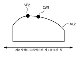
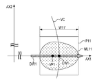
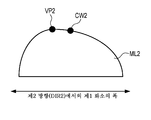
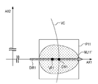
- 101100443272 Arabidopsis thaliana DIR2 gene Proteins 0.000 description 23
- 102100038804 FK506-binding protein-like Human genes 0.000 description 19
- 101001031402 Homo sapiens FK506-binding protein-like Proteins 0.000 description 19
- 230000000052 comparative effect Effects 0.000 description 4
- 230000006870 function Effects 0.000 description 4
- 238000001444 catalytic combustion detection Methods 0.000 description 3
- 230000002093 peripheral effect Effects 0.000 description 3
- 238000010586 diagram Methods 0.000 description 2
- 230000005484 gravity Effects 0.000 description 2
- 230000003321 amplification Effects 0.000 description 1
- 238000003491 array Methods 0.000 description 1
- 238000012986 modification Methods 0.000 description 1
- 230000004048 modification Effects 0.000 description 1
- 238000003199 nucleic acid amplification method Methods 0.000 description 1
- 230000003287 optical effect Effects 0.000 description 1
- 230000001052 transient effect Effects 0.000 description 1
Images


Classifications
-
- H—ELECTRICITY
- H10—SEMICONDUCTOR DEVICES; ELECTRIC SOLID-STATE DEVICES NOT OTHERWISE PROVIDED FOR
- H10F—INORGANIC SEMICONDUCTOR DEVICES SENSITIVE TO INFRARED RADIATION, LIGHT, ELECTROMAGNETIC RADIATION OF SHORTER WAVELENGTH OR CORPUSCULAR RADIATION
- H10F39/00—Integrated devices, or assemblies of multiple devices, comprising at least one element covered by group H10F30/00, e.g. radiation detectors comprising photodiode arrays
- H10F39/10—Integrated devices
- H10F39/12—Image sensors
-
- G—PHYSICS
- G02—OPTICS
- G02B—OPTICAL ELEMENTS, SYSTEMS OR APPARATUS
- G02B3/00—Simple or compound lenses
- G02B3/0006—Arrays
- G02B3/0037—Arrays characterized by the distribution or form of lenses
- G02B3/0043—Inhomogeneous or irregular arrays, e.g. varying shape, size, height
-
- H—ELECTRICITY
- H04—ELECTRIC COMMUNICATION TECHNIQUE
- H04N—PICTORIAL COMMUNICATION, e.g. TELEVISION
- H04N23/00—Cameras or camera modules comprising electronic image sensors; Control thereof
- H04N23/50—Constructional details
- H04N23/54—Mounting of pick-up tubes, electronic image sensors, deviation or focusing coils
-
- H04N5/2254—
-
- G—PHYSICS
- G02—OPTICS
- G02B—OPTICAL ELEMENTS, SYSTEMS OR APPARATUS
- G02B3/00—Simple or compound lenses
- G02B3/0006—Arrays
-
- G—PHYSICS
- G02—OPTICS
- G02B—OPTICAL ELEMENTS, SYSTEMS OR APPARATUS
- G02B3/00—Simple or compound lenses
- G02B3/0006—Arrays
- G02B3/0037—Arrays characterized by the distribution or form of lenses
- G02B3/0056—Arrays characterized by the distribution or form of lenses arranged along two different directions in a plane, e.g. honeycomb arrangement of lenses
-
- G—PHYSICS
- G02—OPTICS
- G02B—OPTICAL ELEMENTS, SYSTEMS OR APPARATUS
- G02B5/00—Optical elements other than lenses
- G02B5/02—Diffusing elements; Afocal elements
- G02B5/0205—Diffusing elements; Afocal elements characterised by the diffusing properties
- G02B5/021—Diffusing elements; Afocal elements characterised by the diffusing properties the diffusion taking place at the element's surface, e.g. by means of surface roughening or microprismatic structures
-
- H—ELECTRICITY
- H04—ELECTRIC COMMUNICATION TECHNIQUE
- H04N—PICTORIAL COMMUNICATION, e.g. TELEVISION
- H04N23/00—Cameras or camera modules comprising electronic image sensors; Control thereof
- H04N23/50—Constructional details
- H04N23/55—Optical parts specially adapted for electronic image sensors; Mounting thereof
-
- H—ELECTRICITY
- H04—ELECTRIC COMMUNICATION TECHNIQUE
- H04N—PICTORIAL COMMUNICATION, e.g. TELEVISION
- H04N25/00—Circuitry of solid-state image sensors [SSIS]; Control thereof
-
- H—ELECTRICITY
- H04—ELECTRIC COMMUNICATION TECHNIQUE
- H04N—PICTORIAL COMMUNICATION, e.g. TELEVISION
- H04N25/00—Circuitry of solid-state image sensors [SSIS]; Control thereof
- H04N25/70—SSIS architectures; Circuits associated therewith
- H04N25/71—Charge-coupled device [CCD] sensors; Charge-transfer registers specially adapted for CCD sensors
-
- H—ELECTRICITY
- H04—ELECTRIC COMMUNICATION TECHNIQUE
- H04N—PICTORIAL COMMUNICATION, e.g. TELEVISION
- H04N25/00—Circuitry of solid-state image sensors [SSIS]; Control thereof
- H04N25/70—SSIS architectures; Circuits associated therewith
- H04N25/76—Addressed sensors, e.g. MOS or CMOS sensors
-
- H04N5/335—
-
- H—ELECTRICITY
- H10—SEMICONDUCTOR DEVICES; ELECTRIC SOLID-STATE DEVICES NOT OTHERWISE PROVIDED FOR
- H10F—INORGANIC SEMICONDUCTOR DEVICES SENSITIVE TO INFRARED RADIATION, LIGHT, ELECTROMAGNETIC RADIATION OF SHORTER WAVELENGTH OR CORPUSCULAR RADIATION
- H10F39/00—Integrated devices, or assemblies of multiple devices, comprising at least one element covered by group H10F30/00, e.g. radiation detectors comprising photodiode arrays
- H10F39/011—Manufacture or treatment of image sensors covered by group H10F39/12
- H10F39/024—Manufacture or treatment of image sensors covered by group H10F39/12 of coatings or optical elements
-
- H—ELECTRICITY
- H10—SEMICONDUCTOR DEVICES; ELECTRIC SOLID-STATE DEVICES NOT OTHERWISE PROVIDED FOR
- H10F—INORGANIC SEMICONDUCTOR DEVICES SENSITIVE TO INFRARED RADIATION, LIGHT, ELECTROMAGNETIC RADIATION OF SHORTER WAVELENGTH OR CORPUSCULAR RADIATION
- H10F39/00—Integrated devices, or assemblies of multiple devices, comprising at least one element covered by group H10F30/00, e.g. radiation detectors comprising photodiode arrays
- H10F39/80—Constructional details of image sensors
- H10F39/806—Optical elements or arrangements associated with the image sensors
- H10F39/8063—Microlenses
-
- G—PHYSICS
- G02—OPTICS
- G02B—OPTICAL ELEMENTS, SYSTEMS OR APPARATUS
- G02B3/00—Simple or compound lenses
- G02B2003/0093—Simple or compound lenses characterised by the shape
Landscapes
- Physics & Mathematics (AREA)
- Engineering & Computer Science (AREA)
- Multimedia (AREA)
- Signal Processing (AREA)
- General Physics & Mathematics (AREA)
- Optics & Photonics (AREA)
- Solid State Image Pick-Up Elements (AREA)
- Transforming Light Signals Into Electric Signals (AREA)
Applications Claiming Priority (2)
| Application Number | Priority Date | Filing Date | Title |
|---|---|---|---|
| JP2015099511A JP6506614B2 (ja) | 2015-05-14 | 2015-05-14 | 固体撮像装置およびカメラ |
| JPJP-P-2015-099511 | 2015-05-14 |
Publications (1)
| Publication Number | Publication Date |
|---|---|
| KR20160134502A true KR20160134502A (ko) | 2016-11-23 |
Family
ID=55802223
Family Applications (1)
| Application Number | Title | Priority Date | Filing Date |
|---|---|---|---|
| KR1020160056116A Ceased KR20160134502A (ko) | 2015-05-14 | 2016-05-09 | 고체 촬상 센서 및 카메라 |
Country Status (9)
| Country | Link |
|---|---|
| US (1) | US10114151B2 (enExample) |
| EP (1) | EP3093887B1 (enExample) |
| JP (1) | JP6506614B2 (enExample) |
| KR (1) | KR20160134502A (enExample) |
| CN (1) | CN106161891B (enExample) |
| BR (1) | BR102016009246A2 (enExample) |
| PH (1) | PH12016000181A1 (enExample) |
| RU (1) | RU2650729C2 (enExample) |
| SG (1) | SG10201603687RA (enExample) |
Cited By (1)
| Publication number | Priority date | Publication date | Assignee | Title |
|---|---|---|---|---|
| EP3293887A1 (en) | 2016-09-08 | 2018-03-14 | Samsung Electronics Co., Ltd. | Near field communication device |
Families Citing this family (6)
| Publication number | Priority date | Publication date | Assignee | Title |
|---|---|---|---|---|
| US10205894B2 (en) | 2015-09-11 | 2019-02-12 | Canon Kabushiki Kaisha | Imaging device and imaging system |
| JP6727938B2 (ja) | 2016-06-10 | 2020-07-22 | キヤノン株式会社 | 撮像装置、撮像装置の制御方法、及び撮像システム |
| JP6688165B2 (ja) | 2016-06-10 | 2020-04-28 | キヤノン株式会社 | 撮像装置及び撮像システム |
| JP6776011B2 (ja) | 2016-06-10 | 2020-10-28 | キヤノン株式会社 | 撮像装置及び撮像システム |
| JP7013119B2 (ja) | 2016-07-21 | 2022-01-31 | キヤノン株式会社 | 固体撮像素子、固体撮像素子の製造方法、及び撮像システム |
| CN109842766B (zh) * | 2018-12-28 | 2021-05-18 | 上海集成电路研发中心有限公司 | 一种极坐标图像传感器及其进行图像处理的方法 |
Family Cites Families (11)
| Publication number | Priority date | Publication date | Assignee | Title |
|---|---|---|---|---|
| US5662401A (en) * | 1995-12-13 | 1997-09-02 | Philips Electronics North America Corporation | Integrating lens array and image forming method for improved optical efficiency |
| US7375892B2 (en) * | 2003-10-09 | 2008-05-20 | Micron Technology, Inc. | Ellipsoidal gapless microlens array and method of fabrication |
| JP2007335723A (ja) | 2006-06-16 | 2007-12-27 | Fujifilm Corp | 固体撮像素子用マイクロレンズ及びその製造方法 |
| US20080011936A1 (en) | 2006-07-14 | 2008-01-17 | Visera Technologies Company Ltd, Roc | Imaging sensor having microlenses of different radii of curvature |
| JP4941233B2 (ja) | 2007-10-31 | 2012-05-30 | 大日本印刷株式会社 | 固体撮像素子およびそれを用いた撮像装置 |
| US7687757B1 (en) * | 2009-01-29 | 2010-03-30 | Visera Technologies Company Limited | Design of microlens on pixel array |
| JP4764958B2 (ja) | 2009-11-20 | 2011-09-07 | 富士フイルム株式会社 | 固体撮像装置 |
| GB2498972A (en) * | 2012-02-01 | 2013-08-07 | St Microelectronics Ltd | Pixel and microlens array |
| JP5791664B2 (ja) | 2013-06-28 | 2015-10-07 | キヤノン株式会社 | 光学素子アレイ、及び固体撮像装置 |
| JP2015109314A (ja) | 2013-12-03 | 2015-06-11 | 株式会社東芝 | 固体撮像装置 |
| JP2016058538A (ja) | 2014-09-09 | 2016-04-21 | キヤノン株式会社 | 固体撮像装置およびカメラ |
-
2015
- 2015-05-14 JP JP2015099511A patent/JP6506614B2/ja not_active Expired - Fee Related
-
2016
- 2016-04-15 EP EP16165488.4A patent/EP3093887B1/en not_active Not-in-force
- 2016-04-22 US US15/136,017 patent/US10114151B2/en active Active
- 2016-04-26 BR BR102016009246A patent/BR102016009246A2/pt not_active Application Discontinuation
- 2016-05-09 KR KR1020160056116A patent/KR20160134502A/ko not_active Ceased
- 2016-05-10 SG SG10201603687RA patent/SG10201603687RA/en unknown
- 2016-05-11 PH PH12016000181A patent/PH12016000181A1/en unknown
- 2016-05-12 RU RU2016118405A patent/RU2650729C2/ru active
- 2016-05-13 CN CN201610317738.XA patent/CN106161891B/zh active Active
Cited By (1)
| Publication number | Priority date | Publication date | Assignee | Title |
|---|---|---|---|---|
| EP3293887A1 (en) | 2016-09-08 | 2018-03-14 | Samsung Electronics Co., Ltd. | Near field communication device |
Also Published As
| Publication number | Publication date |
|---|---|
| RU2016118405A (ru) | 2017-11-16 |
| CN106161891B (zh) | 2019-07-30 |
| JP6506614B2 (ja) | 2019-04-24 |
| RU2650729C2 (ru) | 2018-04-17 |
| PH12016000181A1 (en) | 2018-01-22 |
| SG10201603687RA (en) | 2016-12-29 |
| JP2016219469A (ja) | 2016-12-22 |
| BR102016009246A2 (pt) | 2016-11-16 |
| CN106161891A (zh) | 2016-11-23 |
| US10114151B2 (en) | 2018-10-30 |
| US20160334550A1 (en) | 2016-11-17 |
| EP3093887A1 (en) | 2016-11-16 |
| EP3093887B1 (en) | 2018-01-24 |
Similar Documents
| Publication | Publication Date | Title |
|---|---|---|
| KR20160134502A (ko) | 고체 촬상 센서 및 카메라 | |
| CN206947348U (zh) | 图像传感器 | |
| CN206759600U (zh) | 成像系统 | |
| US10015471B2 (en) | Asymmetric angular response pixels for single sensor stereo | |
| JP2021069118A (ja) | 色分離レンズアレイを具備するイメージセンサ、及びそれを含む電子装置 | |
| KR102765854B1 (ko) | 색분리 렌즈 어레이를 적용한 영상 획득 장치 및 방법 | |
| CN205211754U (zh) | 图像传感器 | |
| JP2011221253A (ja) | 撮像装置、固体撮像素子、撮像方法およびプログラム | |
| CN113037956B (zh) | 成像装置、移动终端和图像感测方法 | |
| JP2017059589A (ja) | 固体撮像素子及び撮像装置 | |
| US20150350529A1 (en) | Image pickup device and image pickup system | |
| US20160073016A1 (en) | Sensor with focus detection units | |
| CN109803129B (zh) | 影像感测器 | |
| US20160286104A1 (en) | Imaging element and imaging device | |
| CN110890390B (zh) | 包括多个成像像素的图像传感器 | |
| JP4884465B2 (ja) | ピクセルアレイ上の非対称マイクロレンズ | |
| JP2007335723A (ja) | 固体撮像素子用マイクロレンズ及びその製造方法 | |
| US10074683B2 (en) | Imaging systems having lens substrates with total internal reflection mitigation structures | |
| US20190268543A1 (en) | Image sensor and focus adjustment device | |
| US20190267422A1 (en) | Image sensor and focus adjustment device | |
| JP2017079243A (ja) | 固体撮像装置及びカメラ | |
| US9955053B2 (en) | Image-capturing assembly and array lens units thereof | |
| JP6492395B2 (ja) | 撮像素子および撮像装置 | |
| JP2012118447A (ja) | 撮像素子およびカメラ | |
| JP2016170212A (ja) | 固体撮像装置およびカメラ |
Legal Events
| Date | Code | Title | Description |
|---|---|---|---|
| PA0109 | Patent application |
Patent event code: PA01091R01D Comment text: Patent Application Patent event date: 20160509 |
|
| PG1501 | Laying open of application | ||
| A201 | Request for examination | ||
| PA0201 | Request for examination |
Patent event code: PA02012R01D Patent event date: 20171109 Comment text: Request for Examination of Application Patent event code: PA02011R01I Patent event date: 20160509 Comment text: Patent Application |
|
| E902 | Notification of reason for refusal | ||
| PE0902 | Notice of grounds for rejection |
Comment text: Notification of reason for refusal Patent event date: 20190221 Patent event code: PE09021S01D |
|
| E601 | Decision to refuse application | ||
| PE0601 | Decision on rejection of patent |
Patent event date: 20190705 Comment text: Decision to Refuse Application Patent event code: PE06012S01D Patent event date: 20190221 Comment text: Notification of reason for refusal Patent event code: PE06011S01I |