EP3093887B1 - Solid-state image sensor and camera - Google Patents
Solid-state image sensor and camera Download PDFInfo
- Publication number
- EP3093887B1 EP3093887B1 EP16165488.4A EP16165488A EP3093887B1 EP 3093887 B1 EP3093887 B1 EP 3093887B1 EP 16165488 A EP16165488 A EP 16165488A EP 3093887 B1 EP3093887 B1 EP 3093887B1
- Authority
- EP
- European Patent Office
- Prior art keywords
- microlens
- image sensor
- solid
- axis
- state image
- Prior art date
- Legal status (The legal status is an assumption and is not a legal conclusion. Google has not performed a legal analysis and makes no representation as to the accuracy of the status listed.)
- Not-in-force
Links
Images


Classifications
-
- H—ELECTRICITY
- H04—ELECTRIC COMMUNICATION TECHNIQUE
- H04N—PICTORIAL COMMUNICATION, e.g. TELEVISION
- H04N23/00—Cameras or camera modules comprising electronic image sensors; Control thereof
- H04N23/50—Constructional details
- H04N23/54—Mounting of pick-up tubes, electronic image sensors, deviation or focusing coils
-
- G—PHYSICS
- G02—OPTICS
- G02B—OPTICAL ELEMENTS, SYSTEMS OR APPARATUS
- G02B3/00—Simple or compound lenses
- G02B3/0006—Arrays
- G02B3/0037—Arrays characterized by the distribution or form of lenses
- G02B3/0043—Inhomogeneous or irregular arrays, e.g. varying shape, size, height
-
- H—ELECTRICITY
- H10—SEMICONDUCTOR DEVICES; ELECTRIC SOLID-STATE DEVICES NOT OTHERWISE PROVIDED FOR
- H10F—INORGANIC SEMICONDUCTOR DEVICES SENSITIVE TO INFRARED RADIATION, LIGHT, ELECTROMAGNETIC RADIATION OF SHORTER WAVELENGTH OR CORPUSCULAR RADIATION
- H10F39/00—Integrated devices, or assemblies of multiple devices, comprising at least one element covered by group H10F30/00, e.g. radiation detectors comprising photodiode arrays
- H10F39/10—Integrated devices
- H10F39/12—Image sensors
-
- G—PHYSICS
- G02—OPTICS
- G02B—OPTICAL ELEMENTS, SYSTEMS OR APPARATUS
- G02B3/00—Simple or compound lenses
- G02B3/0006—Arrays
-
- G—PHYSICS
- G02—OPTICS
- G02B—OPTICAL ELEMENTS, SYSTEMS OR APPARATUS
- G02B3/00—Simple or compound lenses
- G02B3/0006—Arrays
- G02B3/0037—Arrays characterized by the distribution or form of lenses
- G02B3/0056—Arrays characterized by the distribution or form of lenses arranged along two different directions in a plane, e.g. honeycomb arrangement of lenses
-
- G—PHYSICS
- G02—OPTICS
- G02B—OPTICAL ELEMENTS, SYSTEMS OR APPARATUS
- G02B5/00—Optical elements other than lenses
- G02B5/02—Diffusing elements; Afocal elements
- G02B5/0205—Diffusing elements; Afocal elements characterised by the diffusing properties
- G02B5/021—Diffusing elements; Afocal elements characterised by the diffusing properties the diffusion taking place at the element's surface, e.g. by means of surface roughening or microprismatic structures
-
- H—ELECTRICITY
- H04—ELECTRIC COMMUNICATION TECHNIQUE
- H04N—PICTORIAL COMMUNICATION, e.g. TELEVISION
- H04N23/00—Cameras or camera modules comprising electronic image sensors; Control thereof
- H04N23/50—Constructional details
- H04N23/55—Optical parts specially adapted for electronic image sensors; Mounting thereof
-
- H—ELECTRICITY
- H04—ELECTRIC COMMUNICATION TECHNIQUE
- H04N—PICTORIAL COMMUNICATION, e.g. TELEVISION
- H04N25/00—Circuitry of solid-state image sensors [SSIS]; Control thereof
-
- H—ELECTRICITY
- H04—ELECTRIC COMMUNICATION TECHNIQUE
- H04N—PICTORIAL COMMUNICATION, e.g. TELEVISION
- H04N25/00—Circuitry of solid-state image sensors [SSIS]; Control thereof
- H04N25/70—SSIS architectures; Circuits associated therewith
- H04N25/71—Charge-coupled device [CCD] sensors; Charge-transfer registers specially adapted for CCD sensors
-
- H—ELECTRICITY
- H04—ELECTRIC COMMUNICATION TECHNIQUE
- H04N—PICTORIAL COMMUNICATION, e.g. TELEVISION
- H04N25/00—Circuitry of solid-state image sensors [SSIS]; Control thereof
- H04N25/70—SSIS architectures; Circuits associated therewith
- H04N25/76—Addressed sensors, e.g. MOS or CMOS sensors
-
- H—ELECTRICITY
- H10—SEMICONDUCTOR DEVICES; ELECTRIC SOLID-STATE DEVICES NOT OTHERWISE PROVIDED FOR
- H10F—INORGANIC SEMICONDUCTOR DEVICES SENSITIVE TO INFRARED RADIATION, LIGHT, ELECTROMAGNETIC RADIATION OF SHORTER WAVELENGTH OR CORPUSCULAR RADIATION
- H10F39/00—Integrated devices, or assemblies of multiple devices, comprising at least one element covered by group H10F30/00, e.g. radiation detectors comprising photodiode arrays
- H10F39/011—Manufacture or treatment of image sensors covered by group H10F39/12
- H10F39/024—Manufacture or treatment of image sensors covered by group H10F39/12 of coatings or optical elements
-
- H—ELECTRICITY
- H10—SEMICONDUCTOR DEVICES; ELECTRIC SOLID-STATE DEVICES NOT OTHERWISE PROVIDED FOR
- H10F—INORGANIC SEMICONDUCTOR DEVICES SENSITIVE TO INFRARED RADIATION, LIGHT, ELECTROMAGNETIC RADIATION OF SHORTER WAVELENGTH OR CORPUSCULAR RADIATION
- H10F39/00—Integrated devices, or assemblies of multiple devices, comprising at least one element covered by group H10F30/00, e.g. radiation detectors comprising photodiode arrays
- H10F39/80—Constructional details of image sensors
- H10F39/806—Optical elements or arrangements associated with the image sensors
- H10F39/8063—Microlenses
-
- G—PHYSICS
- G02—OPTICS
- G02B—OPTICAL ELEMENTS, SYSTEMS OR APPARATUS
- G02B3/00—Simple or compound lenses
- G02B2003/0093—Simple or compound lenses characterised by the shape
Definitions
- the present invention relates to a solid-state image sensor and a camera.
- JP 2007-335723 describes a non-circular microlens. More specifically, JP 2007-335723 describes a solid-state image sensing element which arranges a microlens having an almost circular shape in a plan view in the central portion of a light-receiving region and arranges a microlens having a teardrop shape in a portion away from the central portion of the light-receiving region.
- the teardrop shape has a long axis and a short axis, and its portion having the maximum width in a direction parallel to the short axis is close to a central portion side in the light-receiving region ( Fig. 2 , and paragraphs 0021 and 0022 of JP 2007-335723 ).
- the direction of the long axis matches a direction of a straight line passing through the central portion of the light-receiving region.
- the teardrop shape is decided in accordance with a distance from the central portion of the light-receiving region.
- JP 2007-335723 An inventive concept described in JP 2007-335723 can be understood to decide the basic shape of the microlens first, and then decide the shape of each microlens by rotating the basic shape in accordance with a position where each microlens should be arranged.
- the microlenses equal to each other in the distance from the central portion are understood to have rotation symmetry.
- the plurality of microlenses each having a rotation-symmetric shape are arrayed in the positions equal to each other in the distance from the central portion, there are more gaps than in arraying a plurality of circular microlenses. This may reduce light collection efficiency.
- Prior art which is related to this field of technology can be found e.g. in document EP 2 819 172 A1 disclosing an optical element array and solid-state imaging device including the array and in document US 2006/0023312 A1 disclosing an ellipsoidal gapless microlens array and method of fabrication.
- the present invention provides a technique advantageous in improving light collection efficiency.
- the present invention in its first aspect provides a solid-state image sensor according to claim 1.
- Fig. 1 shows the arrangement of a solid-state image sensor 1 according to an embodiment of the present invention.
- the solid-state image sensor 1 includes a microlens array MLA in which a plurality of microlenses are arrayed so as to constitute a plurality of rows and a plurality of columns.
- the solid-state image sensor 1 includes a pixel array PA in which a plurality of pixels each including the microlens are arrayed so as to constitute the plurality of rows and the plurality of columns.
- Each pixel which constitutes the pixel array PA includes, in addition to the microlens, a photoelectric converter such as a photodiode.
- Each pixel can also include a color filter.
- Each pixel can further include a circuit in pixel configured to read out a signal from the photoelectric converter.
- Each circuit in pixel can include, for example, an amplification transistor which outputs a signal corresponding to charges generated in the photoelectric converter.
- the solid-state image sensor 1 can further include a peripheral circuit PC.
- the peripheral circuit PC can include, for example, a row selection circuit, a readout circuit, and a column selection circuit.
- the row selection circuit selects each row in the pixel array PA.
- the readout circuit reads out the signals from the pixel array PA.
- the column selection circuit selects, from the signal for one row read out by the readout circuit from the pixel array PA, one signal (the signal corresponding to the column) in a predetermined order. That is, the column selection circuit selects each column in the pixel array PA.
- the solid-state image sensor 1 is constituted by a CCD image sensor
- a plurality of vertical transfer CCDs are arranged in the pixel array PA and the peripheral circuit PC can include a horizontal transfer CCD.
- a first axis AX1 parallel to the plurality of rows of the microlens array MLA and passing through an array center C as the center of the pixel array PA, and a second axis AX2 parallel to the plurality of columns of the microlens array MLA and passing through the array center C are defined for the descriptive convenience.
- a virtual circle VC having the array center C as the center is considered.
- the radius of the virtual circle VC is arbitrary.
- Fig. 1 shows some pixels which are positioned on the virtual circle VC out of the plurality of pixels constituting the pixel array PA. More specifically, Fig.
- first pixels P11, P12, P13, and P14 and a second pixel P2 as the pixels which are positioned on the virtual circle VC out of the plurality of pixels constituting the pixel array PA.
- the first pixels P11, P12, P13, and P14 are positioned on the first axis AX1 or the second axis AX2.
- the second pixel P2 is neither positioned on the first axis AX1 nor the second axis AX2.
- Each pixel positioned on the first axis AX1 or the second axis AX2 can include the pixel with the first axis AX1 or the second axis AX2 crossing in a region of the pixel and/or the pixel with the first axis AX1 or the second axis AX2 contacting the boundary of the region of the pixel.
- Fig. 1 shows only one second pixel P2 though another second pixel exists.
- Each pixel positioned on the virtual circle VC can be defined as a pixel with the virtual circle VC crossing in the region of the pixel.
- Each pixel can have an area of a value obtained by dividing the area of the pixel array PA by the number of pixels and typically be recognized as a polygonal region such as a rectangular region.
- the plurality of microlenses constituting the microlens array MLA include first microlenses ML11, ML12, ML13, and ML14 and a second microlens ML2.
- the first microlenses ML11, ML12, ML13, and ML14 are the microlenses of the first pixels P11, P12, P13, and P14, respectively.
- the second microlens ML2 is the microlens of the second pixel P2. That is, the microlenses positioned on the virtual circle VC out of the plurality of microlenses constituting the microlens array MLA include the first microlenses ML11, ML12, ML13, and ML14 and the second microlens ML2.
- the first microlenses ML11, ML12, ML13, and ML14 are positioned on the first axis AX1 or the second axis AX2.
- the second microlens ML2 is neither positioned on the first axis AX1 nor the second axis AX2.
- An angle formed by the first axis AX1 and a second direction DIR2 can be defined as an argument ⁇ .
- the second direction DIR2 and the argument ⁇ can be understood as a parameter which provides polar coordinates indicating the position of the second microlens ML2 (second pixel P2).
- the second direction DIR2 and the argument ⁇ depend on the position of the second pixel P2.
- each of the first pixels and the second pixel arranged at a predetermined distance or more away from the array center C can include a non-circular bottom shape.
- each of the first pixels and the second pixel arranged at the predetermined distance or less away from the array center C can include a circular bottom shape.
- the predetermined distance can be determined arbitrarily and can be a distance of 10%, 20%, 30%, or 40% of each short side of the pixel array PA.
- each of the first microlenses of the first pixels P11, P12, P13, and P14 and the second microlens of the second pixel P2 has the non-circular bottom shape.
- the width of the second microlens ML2 in the second direction DIR2 passing through the second microlens ML2 and the array center C is larger than the width of the first microlens ML11 in a first direction DIR1 passing through the first microlens ML11 and the array center C.
- the width of the second microlens ML2 in the second direction DIR2 passing through the second microlens ML2 and the array center C is larger than the width of the first microlens ML12 in the first direction DIR1 passing through the first microlens ML12 and the array center C.
- the width of the second microlens ML2 in the second direction DIR2 passing through the second microlens ML2 and the array center C is larger than the width of the first microlens ML13 in the first direction DIR1 passing through the first microlens ML13 and the array center C.
- the width of the second microlens ML2 in the second direction DIR2 passing through the second microlens ML2 and the array center C is larger than the width of the first microlens ML14 in the first direction DIR1 passing through the first microlens ML14 and the array center C.
- the first direction DIR1 passes through the barycenter of each first microlens and the array center C
- the second direction DIR2 passes through the barycenter of the second microlens and the array center.
- the width of the second microlens ML2 in the second direction DIR2 can be increased in accordance with an increase in ⁇ in ranges of 0° ⁇ ⁇ ⁇ 45°, 90° ⁇ ⁇ ⁇ 135°, 180° ⁇ ⁇ ⁇ 225°, and 270° ⁇ ⁇ ⁇ 315°.
- the width of the second microlens ML2 in the second direction DIR2 can be decreased in accordance with the increase in ⁇ in ranges of 45° ⁇ ⁇ ⁇ 90°, 135° ⁇ ⁇ ⁇ 180°, 225° ⁇ ⁇ ⁇ 270°, and 315° ⁇ ⁇ ⁇ 360°.
- Such an arrangement is advantageous in improving light collection efficiency with respect to the photoelectric converter in the second pixel P2.
- each of the first microlenses ML11, ML12, ML13, and ML14 have a line-symmetric shape with respect to a straight line parallel to the first direction DIR1 as a symmetrical axis
- the second microlens ML2 can have a line-symmetric shape with respect to a straight line parallel to the second direction DIR2 as a symmetrical axis.
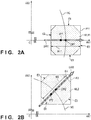
- Figs. 2A and 2B exemplarily show the bottom shapes of the first microlens ML11 and the second microlens ML2 according to the first embodiment of the present invention.
- the bottom shape of each microlens is the shape of a region which is occupied by the microlens projected on a plane parallel to the microlens array MLA.
- a width W2 of the second microlens ML2 in the second direction DIR2 passing through the second microlens ML2 and the array center C is larger than a width W11 of the first microlens ML11 in the first direction DIR1 passing through the first microlens ML11 and the array center C.
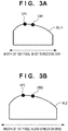
- Fig. 3A shows a cross-sectional shape obtained by cutting the first microlens ML11 shown in Fig. 2A along the straight line parallel to the first direction DIR1.
- Fig. 3B exemplarily shows a cross-sectional shape obtained by cutting the second microlens ML2 shown in Fig. 2B along the straight line parallel to the second direction DIR2.
- a top position VP1 of the first microlens ML11 (ditto for ML12, ML13, and ML14) is at a position shifted to the side of the array center C from a width center CW1 of the first microlens ML11 in the first direction DIR1.
- a top position VP2 of the second microlens ML2 is at a position shifted to the side of the array center C from a width center CW2 of the second microlens ML2 in the second direction DIR2.
- the cross-sectional shape of the second microlens ML2 cut along the straight line parallel to the second direction DIR2 can include a shape obtained by enlarging at least a part of the cross-sectional shape of the first microlens ML11 (ditto for ML12, ML13, and ML14) cut along the straight line parallel to the first direction DIR1. This enlargement may be done with respect to both the first direction DIR1 and a height direction or may be done with respect to only the first direction DIR1.
- the cross-sectional shape of the second microlens ML2 cut along the straight line parallel to the second direction DIR2 may be similar to the cross-sectional shape of the first microlens ML11 (ditto for ML12, ML13, and ML14) cut along the straight line parallel to the first direction DIR1.
- the bottom outer edge of the first microlens ML11 can include a portion E1 parallel to the first direction DIR1 and a portion E2 perpendicular to the first direction DIR1.
- the bottom outer edge of the second microlens ML2 can include a portion E3 parallel to the second direction DIR2 and a portion E4 perpendicular to the second direction DIR2.
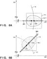
- Figs. 6A, 6B , 7A, and 7B show a comparative example.
- each of a first microlens ML11' and a second microlens ML2' arranged on the virtual circle VC has a rotation-symmetric shape.
- Such an arrangement can be created when the shape of the first microlens ML11' is decided, and then the shape obtained by rotating the first microlens ML11' is decided as the shape of the second microlens ML2'.
- FIG. 6A and 6B exemplarily show the bottom shape of the first microlens ML11' cut along the straight line parallel to the first direction DIR1 and the bottom shape of the second microlens ML2' cut along the straight line parallel to the second direction DIR2.
- Fig. 7A shows a cross-sectional shape obtained by cutting the first microlens ML11' shown in Fig. 6A along the straight line parallel to the first direction DIR1.
- Fig. 7B exemplarily shows a cross-sectional shape obtained by cutting the second microlens ML2' shown in Fig. 6B along the straight line parallel to the second direction DIR2.
- a region 701 outside the outer edge of the second microlens ML2' is larger than in the embodiment shown in Figs. 2A, 2B , 3A, and 3B , and thus light collection efficiency of light to the photoelectric converters is lower than in the embodiment.
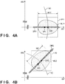
- FIG. 4A and 4B exemplarily show the bottom shapes of a first microlens ML11 and a second microlens ML2 according to the second embodiment of the present invention.
- a width W2' of the second microlens ML2 in a second direction DIR2 passing through the second microlens ML2 and an array center C is larger than a width W11' of the first microlens ML11 in a first direction DIR1 passing through the first microlens ML11 and the array center C.
- Fig. 5A shows a cross-sectional shape obtained by cutting the first microlens ML11 shown in Fig. 4A along a straight line parallel to the first direction DIR1.
- Fig. 5B exemplarily shows a cross-sectional shape obtained by cutting the second microlens ML2 shown in Fig. 4B along a straight line parallel to the second direction DIR2.
- the cross-sectional shape of the second microlens ML2 cut along the straight line parallel to the second direction DIR2 may be similar to the cross-sectional shape of the first microlens ML11 (ditto for ML12, ML13, and ML14) cut along the straight line parallel to the first direction DIR1.
- the concept of the camera includes not only an apparatus mainly aiming at shooting but also an apparatus (for example, a personal computer or a portable terminal) accessorily having a shooting function.
- the camera includes the solid-state image sensor according to the present invention exemplified as the above-described embodiments, and a processor which processes a signal output from the solid-state image sensor.
- the processor can include, for example, an A/D converter and a processor which processes digital data output from the A/D converter.
- Example(s) being useful to understand the present invention can also be realized by a computer of a system or apparatus that reads out and executes computer executable instructions (e.g., one or more programs) recorded on a storage medium (which may also be referred to more fully as a 'non-transitory computer-readable storage medium') to perform the functions of one or more of the above-described embodiment(s) and/or that includes one or more circuits (e.g., application specific integrated circuit (ASIC)) for performing the functions of one or more of the above-described embodiment(s), and by a method performed by the computer of the system or apparatus by, for example, reading out and executing the computer executable instructions from the storage medium to perform the functions of one or more of the above-described embodiment(s) and/or controlling the one or more circuits to perform the functions of one or more of the above-described embodiment(s).
- ASIC application specific integrated circuit
- the computer may comprise one or more processors (e.g., central processing unit (CPU), micro processing unit (MPU)) and may include a network of separate computers or separate processors to read out and execute the computer executable instructions.
- the computer executable instructions may be provided to the computer, for example, from a network or the storage medium.
- the storage medium may include, for example, one or more of a hard disk, a random-access memory (RAM), a read only memory (ROM), a storage of distributed computing systems, an optical disk (such as a compact disc (CD), digital versatile disc (DVD), or Blu-ray Disc (BD)TM), a flash memory device, a memory card, and the like.
Landscapes
- Physics & Mathematics (AREA)
- Engineering & Computer Science (AREA)
- Multimedia (AREA)
- Signal Processing (AREA)
- General Physics & Mathematics (AREA)
- Optics & Photonics (AREA)
- Solid State Image Pick-Up Elements (AREA)
- Transforming Light Signals Into Electric Signals (AREA)
Applications Claiming Priority (1)
| Application Number | Priority Date | Filing Date | Title |
|---|---|---|---|
| JP2015099511A JP6506614B2 (ja) | 2015-05-14 | 2015-05-14 | 固体撮像装置およびカメラ |
Publications (2)
| Publication Number | Publication Date |
|---|---|
| EP3093887A1 EP3093887A1 (en) | 2016-11-16 |
| EP3093887B1 true EP3093887B1 (en) | 2018-01-24 |
Family
ID=55802223
Family Applications (1)
| Application Number | Title | Priority Date | Filing Date |
|---|---|---|---|
| EP16165488.4A Not-in-force EP3093887B1 (en) | 2015-05-14 | 2016-04-15 | Solid-state image sensor and camera |
Country Status (9)
| Country | Link |
|---|---|
| US (1) | US10114151B2 (enExample) |
| EP (1) | EP3093887B1 (enExample) |
| JP (1) | JP6506614B2 (enExample) |
| KR (1) | KR20160134502A (enExample) |
| CN (1) | CN106161891B (enExample) |
| BR (1) | BR102016009246A2 (enExample) |
| PH (1) | PH12016000181A1 (enExample) |
| RU (1) | RU2650729C2 (enExample) |
| SG (1) | SG10201603687RA (enExample) |
Families Citing this family (7)
| Publication number | Priority date | Publication date | Assignee | Title |
|---|---|---|---|---|
| US10205894B2 (en) | 2015-09-11 | 2019-02-12 | Canon Kabushiki Kaisha | Imaging device and imaging system |
| JP6727938B2 (ja) | 2016-06-10 | 2020-07-22 | キヤノン株式会社 | 撮像装置、撮像装置の制御方法、及び撮像システム |
| JP6688165B2 (ja) | 2016-06-10 | 2020-04-28 | キヤノン株式会社 | 撮像装置及び撮像システム |
| JP6776011B2 (ja) | 2016-06-10 | 2020-10-28 | キヤノン株式会社 | 撮像装置及び撮像システム |
| JP7013119B2 (ja) | 2016-07-21 | 2022-01-31 | キヤノン株式会社 | 固体撮像素子、固体撮像素子の製造方法、及び撮像システム |
| US10212576B2 (en) | 2016-09-08 | 2019-02-19 | Samsung Electronics Co., Ltd. | Near field communication device |
| CN109842766B (zh) * | 2018-12-28 | 2021-05-18 | 上海集成电路研发中心有限公司 | 一种极坐标图像传感器及其进行图像处理的方法 |
Family Cites Families (11)
| Publication number | Priority date | Publication date | Assignee | Title |
|---|---|---|---|---|
| US5662401A (en) * | 1995-12-13 | 1997-09-02 | Philips Electronics North America Corporation | Integrating lens array and image forming method for improved optical efficiency |
| US7375892B2 (en) * | 2003-10-09 | 2008-05-20 | Micron Technology, Inc. | Ellipsoidal gapless microlens array and method of fabrication |
| JP2007335723A (ja) | 2006-06-16 | 2007-12-27 | Fujifilm Corp | 固体撮像素子用マイクロレンズ及びその製造方法 |
| US20080011936A1 (en) | 2006-07-14 | 2008-01-17 | Visera Technologies Company Ltd, Roc | Imaging sensor having microlenses of different radii of curvature |
| JP4941233B2 (ja) | 2007-10-31 | 2012-05-30 | 大日本印刷株式会社 | 固体撮像素子およびそれを用いた撮像装置 |
| US7687757B1 (en) * | 2009-01-29 | 2010-03-30 | Visera Technologies Company Limited | Design of microlens on pixel array |
| JP4764958B2 (ja) | 2009-11-20 | 2011-09-07 | 富士フイルム株式会社 | 固体撮像装置 |
| GB2498972A (en) * | 2012-02-01 | 2013-08-07 | St Microelectronics Ltd | Pixel and microlens array |
| JP5791664B2 (ja) | 2013-06-28 | 2015-10-07 | キヤノン株式会社 | 光学素子アレイ、及び固体撮像装置 |
| JP2015109314A (ja) | 2013-12-03 | 2015-06-11 | 株式会社東芝 | 固体撮像装置 |
| JP2016058538A (ja) | 2014-09-09 | 2016-04-21 | キヤノン株式会社 | 固体撮像装置およびカメラ |
-
2015
- 2015-05-14 JP JP2015099511A patent/JP6506614B2/ja not_active Expired - Fee Related
-
2016
- 2016-04-15 EP EP16165488.4A patent/EP3093887B1/en not_active Not-in-force
- 2016-04-22 US US15/136,017 patent/US10114151B2/en active Active
- 2016-04-26 BR BR102016009246A patent/BR102016009246A2/pt not_active Application Discontinuation
- 2016-05-09 KR KR1020160056116A patent/KR20160134502A/ko not_active Ceased
- 2016-05-10 SG SG10201603687RA patent/SG10201603687RA/en unknown
- 2016-05-11 PH PH12016000181A patent/PH12016000181A1/en unknown
- 2016-05-12 RU RU2016118405A patent/RU2650729C2/ru active
- 2016-05-13 CN CN201610317738.XA patent/CN106161891B/zh active Active
Non-Patent Citations (1)
| Title |
|---|
| None * |
Also Published As
| Publication number | Publication date |
|---|---|
| RU2016118405A (ru) | 2017-11-16 |
| CN106161891B (zh) | 2019-07-30 |
| JP6506614B2 (ja) | 2019-04-24 |
| RU2650729C2 (ru) | 2018-04-17 |
| PH12016000181A1 (en) | 2018-01-22 |
| SG10201603687RA (en) | 2016-12-29 |
| JP2016219469A (ja) | 2016-12-22 |
| BR102016009246A2 (pt) | 2016-11-16 |
| CN106161891A (zh) | 2016-11-23 |
| US10114151B2 (en) | 2018-10-30 |
| US20160334550A1 (en) | 2016-11-17 |
| KR20160134502A (ko) | 2016-11-23 |
| EP3093887A1 (en) | 2016-11-16 |
Similar Documents
| Publication | Publication Date | Title |
|---|---|---|
| EP3093887B1 (en) | Solid-state image sensor and camera | |
| CN206947348U (zh) | 图像传感器 | |
| CN206759600U (zh) | 成像系统 | |
| CN205211754U (zh) | 图像传感器 | |
| JP2021069118A (ja) | 色分離レンズアレイを具備するイメージセンサ、及びそれを含む電子装置 | |
| US9883128B2 (en) | Imaging systems with high dynamic range and phase detection pixels | |
| JP5744545B2 (ja) | 固体撮像装置およびカメラ | |
| JP7012619B2 (ja) | 撮像素子および撮像装置 | |
| CN113037956B (zh) | 成像装置、移动终端和图像感测方法 | |
| US9729806B2 (en) | Imaging systems with phase detection pixels | |
| US20160073016A1 (en) | Sensor with focus detection units | |
| JP2015228466A (ja) | 撮像装置及び撮像システム | |
| JP6561836B2 (ja) | 撮像素子および撮像装置 | |
| JP4884465B2 (ja) | ピクセルアレイ上の非対称マイクロレンズ | |
| CN112786629B (zh) | 图像传感器 | |
| JP6195134B2 (ja) | 電磁波検知器アセンブリを備える装置およびそのような装置のアセンブリの配置 | |
| US20160141323A1 (en) | Solid-state imaging apparatus | |
| JP6492395B2 (ja) | 撮像素子および撮像装置 | |
| JP2012252646A (ja) | 画像処理システムおよび画像処理方法 | |
| JP2015180077A (ja) | 固体撮像装置およびカメラ | |
| CN117981342A (zh) | 用于控制图像传感器的系统和方法 |
Legal Events
| Date | Code | Title | Description |
|---|---|---|---|
| PUAI | Public reference made under article 153(3) epc to a published international application that has entered the european phase |
Free format text: ORIGINAL CODE: 0009012 |
|
| AK | Designated contracting states |
Kind code of ref document: A1 Designated state(s): AL AT BE BG CH CY CZ DE DK EE ES FI FR GB GR HR HU IE IS IT LI LT LU LV MC MK MT NL NO PL PT RO RS SE SI SK SM TR |
|
| AX | Request for extension of the european patent |
Extension state: BA ME |
|
| 17P | Request for examination filed |
Effective date: 20170516 |
|
| RBV | Designated contracting states (corrected) |
Designated state(s): AL AT BE BG CH CY CZ DE DK EE ES FI FR GB GR HR HU IE IS IT LI LT LU LV MC MK MT NL NO PL PT RO RS SE SI SK SM TR |
|
| GRAP | Despatch of communication of intention to grant a patent |
Free format text: ORIGINAL CODE: EPIDOSNIGR1 |
|
| INTG | Intention to grant announced |
Effective date: 20170803 |
|
| RIN1 | Information on inventor provided before grant (corrected) |
Inventor name: KAWABATA, KAZUNARI |
|
| GRAS | Grant fee paid |
Free format text: ORIGINAL CODE: EPIDOSNIGR3 |
|
| GRAA | (expected) grant |
Free format text: ORIGINAL CODE: 0009210 |
|
| AK | Designated contracting states |
Kind code of ref document: B1 Designated state(s): AL AT BE BG CH CY CZ DE DK EE ES FI FR GB GR HR HU IE IS IT LI LT LU LV MC MK MT NL NO PL PT RO RS SE SI SK SM TR |
|
| REG | Reference to a national code |
Ref country code: GB Ref legal event code: FG4D |
|
| REG | Reference to a national code |
Ref country code: CH Ref legal event code: EP |
|
| REG | Reference to a national code |
Ref country code: AT Ref legal event code: REF Ref document number: 966230 Country of ref document: AT Kind code of ref document: T Effective date: 20180215 |
|
| REG | Reference to a national code |
Ref country code: IE Ref legal event code: FG4D |
|
| REG | Reference to a national code |
Ref country code: DE Ref legal event code: R096 Ref document number: 602016001433 Country of ref document: DE |
|
| REG | Reference to a national code |
Ref country code: NL Ref legal event code: MP Effective date: 20180124 |
|
| REG | Reference to a national code |
Ref country code: LT Ref legal event code: MG4D |
|
| REG | Reference to a national code |
Ref country code: AT Ref legal event code: MK05 Ref document number: 966230 Country of ref document: AT Kind code of ref document: T Effective date: 20180124 |
|
| PG25 | Lapsed in a contracting state [announced via postgrant information from national office to epo] |
Ref country code: NL Free format text: LAPSE BECAUSE OF FAILURE TO SUBMIT A TRANSLATION OF THE DESCRIPTION OR TO PAY THE FEE WITHIN THE PRESCRIBED TIME-LIMIT Effective date: 20180124 |
|
| PG25 | Lapsed in a contracting state [announced via postgrant information from national office to epo] |
Ref country code: LT Free format text: LAPSE BECAUSE OF FAILURE TO SUBMIT A TRANSLATION OF THE DESCRIPTION OR TO PAY THE FEE WITHIN THE PRESCRIBED TIME-LIMIT Effective date: 20180124 Ref country code: NO Free format text: LAPSE BECAUSE OF FAILURE TO SUBMIT A TRANSLATION OF THE DESCRIPTION OR TO PAY THE FEE WITHIN THE PRESCRIBED TIME-LIMIT Effective date: 20180424 Ref country code: ES Free format text: LAPSE BECAUSE OF FAILURE TO SUBMIT A TRANSLATION OF THE DESCRIPTION OR TO PAY THE FEE WITHIN THE PRESCRIBED TIME-LIMIT Effective date: 20180124 Ref country code: HR Free format text: LAPSE BECAUSE OF FAILURE TO SUBMIT A TRANSLATION OF THE DESCRIPTION OR TO PAY THE FEE WITHIN THE PRESCRIBED TIME-LIMIT Effective date: 20180124 Ref country code: FI Free format text: LAPSE BECAUSE OF FAILURE TO SUBMIT A TRANSLATION OF THE DESCRIPTION OR TO PAY THE FEE WITHIN THE PRESCRIBED TIME-LIMIT Effective date: 20180124 Ref country code: CY Free format text: LAPSE BECAUSE OF FAILURE TO SUBMIT A TRANSLATION OF THE DESCRIPTION OR TO PAY THE FEE WITHIN THE PRESCRIBED TIME-LIMIT Effective date: 20180124 |
|
| PG25 | Lapsed in a contracting state [announced via postgrant information from national office to epo] |
Ref country code: LV Free format text: LAPSE BECAUSE OF FAILURE TO SUBMIT A TRANSLATION OF THE DESCRIPTION OR TO PAY THE FEE WITHIN THE PRESCRIBED TIME-LIMIT Effective date: 20180124 Ref country code: SE Free format text: LAPSE BECAUSE OF FAILURE TO SUBMIT A TRANSLATION OF THE DESCRIPTION OR TO PAY THE FEE WITHIN THE PRESCRIBED TIME-LIMIT Effective date: 20180124 Ref country code: GR Free format text: LAPSE BECAUSE OF FAILURE TO SUBMIT A TRANSLATION OF THE DESCRIPTION OR TO PAY THE FEE WITHIN THE PRESCRIBED TIME-LIMIT Effective date: 20180425 Ref country code: PL Free format text: LAPSE BECAUSE OF FAILURE TO SUBMIT A TRANSLATION OF THE DESCRIPTION OR TO PAY THE FEE WITHIN THE PRESCRIBED TIME-LIMIT Effective date: 20180124 Ref country code: BG Free format text: LAPSE BECAUSE OF FAILURE TO SUBMIT A TRANSLATION OF THE DESCRIPTION OR TO PAY THE FEE WITHIN THE PRESCRIBED TIME-LIMIT Effective date: 20180424 Ref country code: IS Free format text: LAPSE BECAUSE OF FAILURE TO SUBMIT A TRANSLATION OF THE DESCRIPTION OR TO PAY THE FEE WITHIN THE PRESCRIBED TIME-LIMIT Effective date: 20180524 Ref country code: RS Free format text: LAPSE BECAUSE OF FAILURE TO SUBMIT A TRANSLATION OF THE DESCRIPTION OR TO PAY THE FEE WITHIN THE PRESCRIBED TIME-LIMIT Effective date: 20180124 Ref country code: AT Free format text: LAPSE BECAUSE OF FAILURE TO SUBMIT A TRANSLATION OF THE DESCRIPTION OR TO PAY THE FEE WITHIN THE PRESCRIBED TIME-LIMIT Effective date: 20180124 |
|
| REG | Reference to a national code |
Ref country code: DE Ref legal event code: R097 Ref document number: 602016001433 Country of ref document: DE |
|
| PG25 | Lapsed in a contracting state [announced via postgrant information from national office to epo] |
Ref country code: IT Free format text: LAPSE BECAUSE OF FAILURE TO SUBMIT A TRANSLATION OF THE DESCRIPTION OR TO PAY THE FEE WITHIN THE PRESCRIBED TIME-LIMIT Effective date: 20180124 Ref country code: AL Free format text: LAPSE BECAUSE OF FAILURE TO SUBMIT A TRANSLATION OF THE DESCRIPTION OR TO PAY THE FEE WITHIN THE PRESCRIBED TIME-LIMIT Effective date: 20180124 Ref country code: EE Free format text: LAPSE BECAUSE OF FAILURE TO SUBMIT A TRANSLATION OF THE DESCRIPTION OR TO PAY THE FEE WITHIN THE PRESCRIBED TIME-LIMIT Effective date: 20180124 |
|
| PG25 | Lapsed in a contracting state [announced via postgrant information from national office to epo] |
Ref country code: SM Free format text: LAPSE BECAUSE OF FAILURE TO SUBMIT A TRANSLATION OF THE DESCRIPTION OR TO PAY THE FEE WITHIN THE PRESCRIBED TIME-LIMIT Effective date: 20180124 Ref country code: CZ Free format text: LAPSE BECAUSE OF FAILURE TO SUBMIT A TRANSLATION OF THE DESCRIPTION OR TO PAY THE FEE WITHIN THE PRESCRIBED TIME-LIMIT Effective date: 20180124 Ref country code: MC Free format text: LAPSE BECAUSE OF FAILURE TO SUBMIT A TRANSLATION OF THE DESCRIPTION OR TO PAY THE FEE WITHIN THE PRESCRIBED TIME-LIMIT Effective date: 20180124 Ref country code: DK Free format text: LAPSE BECAUSE OF FAILURE TO SUBMIT A TRANSLATION OF THE DESCRIPTION OR TO PAY THE FEE WITHIN THE PRESCRIBED TIME-LIMIT Effective date: 20180124 Ref country code: SK Free format text: LAPSE BECAUSE OF FAILURE TO SUBMIT A TRANSLATION OF THE DESCRIPTION OR TO PAY THE FEE WITHIN THE PRESCRIBED TIME-LIMIT Effective date: 20180124 |
|
| PLBE | No opposition filed within time limit |
Free format text: ORIGINAL CODE: 0009261 |
|
| STAA | Information on the status of an ep patent application or granted ep patent |
Free format text: STATUS: NO OPPOSITION FILED WITHIN TIME LIMIT |
|
| REG | Reference to a national code |
Ref country code: BE Ref legal event code: MM Effective date: 20180430 |
|
| 26N | No opposition filed |
Effective date: 20181025 |
|
| REG | Reference to a national code |
Ref country code: IE Ref legal event code: MM4A |
|
| PG25 | Lapsed in a contracting state [announced via postgrant information from national office to epo] |
Ref country code: LU Free format text: LAPSE BECAUSE OF NON-PAYMENT OF DUE FEES Effective date: 20180415 |
|
| PG25 | Lapsed in a contracting state [announced via postgrant information from national office to epo] |
Ref country code: BE Free format text: LAPSE BECAUSE OF NON-PAYMENT OF DUE FEES Effective date: 20180430 Ref country code: SI Free format text: LAPSE BECAUSE OF FAILURE TO SUBMIT A TRANSLATION OF THE DESCRIPTION OR TO PAY THE FEE WITHIN THE PRESCRIBED TIME-LIMIT Effective date: 20180124 |
|
| PG25 | Lapsed in a contracting state [announced via postgrant information from national office to epo] |
Ref country code: IE Free format text: LAPSE BECAUSE OF NON-PAYMENT OF DUE FEES Effective date: 20180415 Ref country code: FR Free format text: LAPSE BECAUSE OF NON-PAYMENT OF DUE FEES Effective date: 20180430 |
|
| REG | Reference to a national code |
Ref country code: CH Ref legal event code: PL |
|
| PG25 | Lapsed in a contracting state [announced via postgrant information from national office to epo] |
Ref country code: LI Free format text: LAPSE BECAUSE OF NON-PAYMENT OF DUE FEES Effective date: 20190430 Ref country code: CH Free format text: LAPSE BECAUSE OF NON-PAYMENT OF DUE FEES Effective date: 20190430 Ref country code: MT Free format text: LAPSE BECAUSE OF NON-PAYMENT OF DUE FEES Effective date: 20180415 |
|
| PG25 | Lapsed in a contracting state [announced via postgrant information from national office to epo] |
Ref country code: TR Free format text: LAPSE BECAUSE OF FAILURE TO SUBMIT A TRANSLATION OF THE DESCRIPTION OR TO PAY THE FEE WITHIN THE PRESCRIBED TIME-LIMIT Effective date: 20180124 |
|
| PG25 | Lapsed in a contracting state [announced via postgrant information from national office to epo] |
Ref country code: PT Free format text: LAPSE BECAUSE OF FAILURE TO SUBMIT A TRANSLATION OF THE DESCRIPTION OR TO PAY THE FEE WITHIN THE PRESCRIBED TIME-LIMIT Effective date: 20180124 |
|
| PG25 | Lapsed in a contracting state [announced via postgrant information from national office to epo] |
Ref country code: RO Free format text: LAPSE BECAUSE OF FAILURE TO SUBMIT A TRANSLATION OF THE DESCRIPTION OR TO PAY THE FEE WITHIN THE PRESCRIBED TIME-LIMIT Effective date: 20180124 Ref country code: HU Free format text: LAPSE BECAUSE OF FAILURE TO SUBMIT A TRANSLATION OF THE DESCRIPTION OR TO PAY THE FEE WITHIN THE PRESCRIBED TIME-LIMIT; INVALID AB INITIO Effective date: 20160415 Ref country code: MK Free format text: LAPSE BECAUSE OF NON-PAYMENT OF DUE FEES Effective date: 20180124 |
|
| GBPC | Gb: european patent ceased through non-payment of renewal fee |
Effective date: 20200415 |
|
| PG25 | Lapsed in a contracting state [announced via postgrant information from national office to epo] |
Ref country code: GB Free format text: LAPSE BECAUSE OF NON-PAYMENT OF DUE FEES Effective date: 20200415 |
|
| PGFP | Annual fee paid to national office [announced via postgrant information from national office to epo] |
Ref country code: DE Payment date: 20230321 Year of fee payment: 8 |
|
| REG | Reference to a national code |
Ref country code: DE Ref legal event code: R079 Ref document number: 602016001433 Country of ref document: DE Free format text: PREVIOUS MAIN CLASS: H01L0027146000 Ipc: H10F0039180000 |
|
| REG | Reference to a national code |
Ref country code: DE Ref legal event code: R119 Ref document number: 602016001433 Country of ref document: DE |
|
| PG25 | Lapsed in a contracting state [announced via postgrant information from national office to epo] |
Ref country code: DE Free format text: LAPSE BECAUSE OF NON-PAYMENT OF DUE FEES Effective date: 20251104 |