KR102491746B1 - 완전히 자기 정렬된 비아를 형성하기 위한 선택적 막 퇴적 방법 - Google Patents
완전히 자기 정렬된 비아를 형성하기 위한 선택적 막 퇴적 방법 Download PDFInfo
- Publication number
- KR102491746B1 KR102491746B1 KR1020180143517A KR20180143517A KR102491746B1 KR 102491746 B1 KR102491746 B1 KR 102491746B1 KR 1020180143517 A KR1020180143517 A KR 1020180143517A KR 20180143517 A KR20180143517 A KR 20180143517A KR 102491746 B1 KR102491746 B1 KR 102491746B1
- Authority
- KR
- South Korea
- Prior art keywords
- substrate
- gas
- film
- sio
- exposing
- Prior art date
- Legal status (The legal status is an assumption and is not a legal conclusion. Google has not performed a legal analysis and makes no representation as to the accuracy of the status listed.)
- Active
Links
- 238000000034 method Methods 0.000 title claims abstract description 99
- 230000008021 deposition Effects 0.000 title claims description 37
- 239000000758 substrate Substances 0.000 claims abstract description 122
- 238000012545 processing Methods 0.000 claims abstract description 81
- 230000008569 process Effects 0.000 claims abstract description 69
- 229910004298 SiO 2 Inorganic materials 0.000 claims abstract description 44
- 238000003672 processing method Methods 0.000 claims abstract description 7
- 239000007789 gas Substances 0.000 claims description 109
- 229910052751 metal Inorganic materials 0.000 claims description 68
- 239000002184 metal Substances 0.000 claims description 68
- 238000000151 deposition Methods 0.000 claims description 47
- 239000003054 catalyst Substances 0.000 claims description 36
- 239000010936 titanium Substances 0.000 claims description 35
- SCPYDCQAZCOKTP-UHFFFAOYSA-N silanol Chemical compound [SiH3]O SCPYDCQAZCOKTP-UHFFFAOYSA-N 0.000 claims description 22
- 238000004140 cleaning Methods 0.000 claims description 15
- 239000000376 reactant Substances 0.000 claims description 14
- 239000003989 dielectric material Substances 0.000 claims description 10
- KFZMGEQAYNKOFK-UHFFFAOYSA-N Isopropanol Chemical compound CC(C)O KFZMGEQAYNKOFK-UHFFFAOYSA-N 0.000 claims description 9
- LFQSCWFLJHTTHZ-UHFFFAOYSA-N Ethanol Chemical compound CCO LFQSCWFLJHTTHZ-UHFFFAOYSA-N 0.000 claims description 8
- XOJVVFBFDXDTEG-UHFFFAOYSA-N Norphytane Natural products CC(C)CCCC(C)CCCC(C)CCCC(C)C XOJVVFBFDXDTEG-UHFFFAOYSA-N 0.000 claims description 7
- OKKJLVBELUTLKV-UHFFFAOYSA-N Methanol Chemical compound OC OKKJLVBELUTLKV-UHFFFAOYSA-N 0.000 claims description 6
- 229910052782 aluminium Inorganic materials 0.000 claims description 6
- 229910052719 titanium Inorganic materials 0.000 claims description 6
- XAGFODPZIPBFFR-UHFFFAOYSA-N aluminium Chemical compound [Al] XAGFODPZIPBFFR-UHFFFAOYSA-N 0.000 claims description 4
- ORJFXWYTRPGGRK-UHFFFAOYSA-N hydroxy-tris(2-methylbutan-2-yloxy)silane Chemical compound CCC(C)(C)O[Si](O)(OC(C)(C)CC)OC(C)(C)CC ORJFXWYTRPGGRK-UHFFFAOYSA-N 0.000 claims description 3
- 239000011261 inert gas Substances 0.000 claims description 3
- 239000012495 reaction gas Substances 0.000 claims description 3
- RTAQQCXQSZGOHL-UHFFFAOYSA-N Titanium Chemical compound [Ti] RTAQQCXQSZGOHL-UHFFFAOYSA-N 0.000 claims description 2
- 239000003795 chemical substances by application Substances 0.000 claims description 2
- 229910052735 hafnium Inorganic materials 0.000 claims description 2
- VBJZVLUMGGDVMO-UHFFFAOYSA-N hafnium atom Chemical compound [Hf] VBJZVLUMGGDVMO-UHFFFAOYSA-N 0.000 claims description 2
- 230000003301 hydrolyzing effect Effects 0.000 claims description 2
- MBMITMZVBNZJTQ-UHFFFAOYSA-N hydroxy-bis[(2-methylpropan-2-yl)oxy]-propan-2-yloxysilane Chemical compound CC(C)O[Si](O)(OC(C)(C)C)OC(C)(C)C MBMITMZVBNZJTQ-UHFFFAOYSA-N 0.000 claims description 2
- HLDBBQREZCVBMA-UHFFFAOYSA-N hydroxy-tris[(2-methylpropan-2-yl)oxy]silane Chemical compound CC(C)(C)O[Si](O)(OC(C)(C)C)OC(C)(C)C HLDBBQREZCVBMA-UHFFFAOYSA-N 0.000 claims description 2
- 230000001590 oxidative effect Effects 0.000 claims description 2
- VSZWPYCFIRKVQL-UHFFFAOYSA-N selanylidenegallium;selenium Chemical compound [Se].[Se]=[Ga].[Se]=[Ga] VSZWPYCFIRKVQL-UHFFFAOYSA-N 0.000 claims description 2
- FGUUSXIOTUKUDN-IBGZPJMESA-N C1(=CC=CC=C1)N1C2=C(NC([C@H](C1)NC=1OC(=NN=1)C1=CC=CC=C1)=O)C=CC=C2 Chemical compound C1(=CC=CC=C1)N1C2=C(NC([C@H](C1)NC=1OC(=NN=1)C1=CC=CC=C1)=O)C=CC=C2 FGUUSXIOTUKUDN-IBGZPJMESA-N 0.000 claims 1
- JLTRXTDYQLMHGR-UHFFFAOYSA-N trimethylaluminium Chemical compound C[Al](C)C JLTRXTDYQLMHGR-UHFFFAOYSA-N 0.000 claims 1
- 239000010410 layer Substances 0.000 description 43
- 239000010408 film Substances 0.000 description 39
- 239000000463 material Substances 0.000 description 25
- 235000012431 wafers Nutrition 0.000 description 19
- 238000012546 transfer Methods 0.000 description 17
- 239000002243 precursor Substances 0.000 description 12
- 238000010926 purge Methods 0.000 description 12
- VYPSYNLAJGMNEJ-UHFFFAOYSA-N Silicium dioxide Chemical compound O=[Si]=O VYPSYNLAJGMNEJ-UHFFFAOYSA-N 0.000 description 10
- 230000007246 mechanism Effects 0.000 description 6
- 239000004065 semiconductor Substances 0.000 description 6
- -1 SiCOH Inorganic materials 0.000 description 5
- 229910052681 coesite Inorganic materials 0.000 description 5
- 229910052906 cristobalite Inorganic materials 0.000 description 5
- 238000005192 partition Methods 0.000 description 5
- 230000002093 peripheral effect Effects 0.000 description 5
- 239000000377 silicon dioxide Substances 0.000 description 5
- 235000012239 silicon dioxide Nutrition 0.000 description 5
- 229910052682 stishovite Inorganic materials 0.000 description 5
- 229910052905 tridymite Inorganic materials 0.000 description 5
- XKRFYHLGVUSROY-UHFFFAOYSA-N Argon Chemical compound [Ar] XKRFYHLGVUSROY-UHFFFAOYSA-N 0.000 description 4
- 239000003446 ligand Substances 0.000 description 4
- 238000001179 sorption measurement Methods 0.000 description 4
- 150000001298 alcohols Chemical class 0.000 description 3
- 230000004888 barrier function Effects 0.000 description 3
- 239000002356 single layer Substances 0.000 description 3
- 239000010409 thin film Substances 0.000 description 3
- IJGRMHOSHXDMSA-UHFFFAOYSA-N Atomic nitrogen Chemical compound N#N IJGRMHOSHXDMSA-UHFFFAOYSA-N 0.000 description 2
- ATJFFYVFTNAWJD-UHFFFAOYSA-N Tin Chemical compound [Sn] ATJFFYVFTNAWJD-UHFFFAOYSA-N 0.000 description 2
- 239000000956 alloy Substances 0.000 description 2
- 229910045601 alloy Inorganic materials 0.000 description 2
- 229910052786 argon Inorganic materials 0.000 description 2
- QVGXLLKOCUKJST-UHFFFAOYSA-N atomic oxygen Chemical compound [O] QVGXLLKOCUKJST-UHFFFAOYSA-N 0.000 description 2
- 239000012159 carrier gas Substances 0.000 description 2
- 238000001816 cooling Methods 0.000 description 2
- 238000005137 deposition process Methods 0.000 description 2
- 238000009792 diffusion process Methods 0.000 description 2
- 238000005516 engineering process Methods 0.000 description 2
- 238000002955 isolation Methods 0.000 description 2
- 238000004519 manufacturing process Methods 0.000 description 2
- 238000012544 monitoring process Methods 0.000 description 2
- 239000001301 oxygen Substances 0.000 description 2
- 229910052760 oxygen Inorganic materials 0.000 description 2
- 229910052718 tin Inorganic materials 0.000 description 2
- 230000007723 transport mechanism Effects 0.000 description 2
- 229910018072 Al 2 O 3 Inorganic materials 0.000 description 1
- 229910017083 AlN Inorganic materials 0.000 description 1
- 229910017109 AlON Inorganic materials 0.000 description 1
- 229910018565 CuAl Inorganic materials 0.000 description 1
- UFHFLCQGNIYNRP-UHFFFAOYSA-N Hydrogen Chemical compound [H][H] UFHFLCQGNIYNRP-UHFFFAOYSA-N 0.000 description 1
- 229910004491 TaAlN Inorganic materials 0.000 description 1
- 229910004166 TaN Inorganic materials 0.000 description 1
- 229910004200 TaSiN Inorganic materials 0.000 description 1
- 229910010041 TiAlC Inorganic materials 0.000 description 1
- 229910010037 TiAlN Inorganic materials 0.000 description 1
- 229910010413 TiO 2 Inorganic materials 0.000 description 1
- 229910010282 TiON Inorganic materials 0.000 description 1
- 229910008482 TiSiN Inorganic materials 0.000 description 1
- 229910011208 Ti—N Inorganic materials 0.000 description 1
- 238000010521 absorption reaction Methods 0.000 description 1
- 150000004703 alkoxides Chemical class 0.000 description 1
- 125000000217 alkyl group Chemical group 0.000 description 1
- 150000001408 amides Chemical class 0.000 description 1
- 150000001412 amines Chemical class 0.000 description 1
- 125000000129 anionic group Chemical group 0.000 description 1
- 150000007942 carboxylates Chemical class 0.000 description 1
- 230000003197 catalytic effect Effects 0.000 description 1
- 230000008859 change Effects 0.000 description 1
- 238000006243 chemical reaction Methods 0.000 description 1
- 239000011248 coating agent Substances 0.000 description 1
- 238000000576 coating method Methods 0.000 description 1
- 238000011109 contamination Methods 0.000 description 1
- 238000007796 conventional method Methods 0.000 description 1
- 150000003983 crown ethers Chemical class 0.000 description 1
- 125000000058 cyclopentadienyl group Chemical group C1(=CC=CC1)* 0.000 description 1
- 239000012636 effector Substances 0.000 description 1
- 238000000572 ellipsometry Methods 0.000 description 1
- ZSWFCLXCOIISFI-UHFFFAOYSA-N endo-cyclopentadiene Natural products C1C=CC=C1 ZSWFCLXCOIISFI-UHFFFAOYSA-N 0.000 description 1
- 150000002170 ethers Chemical class 0.000 description 1
- 230000006870 function Effects 0.000 description 1
- 150000002240 furans Chemical class 0.000 description 1
- 239000007792 gaseous phase Substances 0.000 description 1
- 150000004820 halides Chemical class 0.000 description 1
- 229910052736 halogen Inorganic materials 0.000 description 1
- 239000001307 helium Substances 0.000 description 1
- 229910052734 helium Inorganic materials 0.000 description 1
- SWQJXJOGLNCZEY-UHFFFAOYSA-N helium atom Chemical compound [He] SWQJXJOGLNCZEY-UHFFFAOYSA-N 0.000 description 1
- 239000001257 hydrogen Substances 0.000 description 1
- 229910052739 hydrogen Inorganic materials 0.000 description 1
- 238000007689 inspection Methods 0.000 description 1
- QRXWMOHMRWLFEY-UHFFFAOYSA-N isoniazide Chemical compound NNC(=O)C1=CC=NC=C1 QRXWMOHMRWLFEY-UHFFFAOYSA-N 0.000 description 1
- 125000003253 isopropoxy group Chemical group [H]C([H])([H])C([H])(O*)C([H])([H])[H] 0.000 description 1
- 229910052743 krypton Inorganic materials 0.000 description 1
- DNNSSWSSYDEUBZ-UHFFFAOYSA-N krypton atom Chemical compound [Kr] DNNSSWSSYDEUBZ-UHFFFAOYSA-N 0.000 description 1
- 239000004973 liquid crystal related substance Substances 0.000 description 1
- 238000001459 lithography Methods 0.000 description 1
- 238000000691 measurement method Methods 0.000 description 1
- 229910044991 metal oxide Inorganic materials 0.000 description 1
- 150000004706 metal oxides Chemical class 0.000 description 1
- 239000000203 mixture Substances 0.000 description 1
- 238000012986 modification Methods 0.000 description 1
- 230000004048 modification Effects 0.000 description 1
- 229910052754 neon Inorganic materials 0.000 description 1
- GKAOGPIIYCISHV-UHFFFAOYSA-N neon atom Chemical compound [Ne] GKAOGPIIYCISHV-UHFFFAOYSA-N 0.000 description 1
- 230000007935 neutral effect Effects 0.000 description 1
- 150000004767 nitrides Chemical class 0.000 description 1
- 150000002825 nitriles Chemical class 0.000 description 1
- 229910052757 nitrogen Inorganic materials 0.000 description 1
- QJGQUHMNIGDVPM-UHFFFAOYSA-N nitrogen group Chemical group [N] QJGQUHMNIGDVPM-UHFFFAOYSA-N 0.000 description 1
- 229910052756 noble gas Inorganic materials 0.000 description 1
- 125000001181 organosilyl group Chemical group [SiH3]* 0.000 description 1
- 239000002245 particle Substances 0.000 description 1
- 238000000059 patterning Methods 0.000 description 1
- 230000000149 penetrating effect Effects 0.000 description 1
- 238000012805 post-processing Methods 0.000 description 1
- 150000003138 primary alcohols Chemical class 0.000 description 1
- 150000003222 pyridines Chemical class 0.000 description 1
- 150000003233 pyrroles Chemical class 0.000 description 1
- 150000003235 pyrrolidines Chemical class 0.000 description 1
- 150000003333 secondary alcohols Chemical class 0.000 description 1
- 238000007560 sedimentation technique Methods 0.000 description 1
- 239000000243 solution Substances 0.000 description 1
- 238000006467 substitution reaction Methods 0.000 description 1
- MNWRORMXBIWXCI-UHFFFAOYSA-N tetrakis(dimethylamido)titanium Chemical compound CN(C)[Ti](N(C)C)(N(C)C)N(C)C MNWRORMXBIWXCI-UHFFFAOYSA-N 0.000 description 1
- 239000012808 vapor phase Substances 0.000 description 1
- 229910052724 xenon Inorganic materials 0.000 description 1
- FHNFHKCVQCLJFQ-UHFFFAOYSA-N xenon atom Chemical compound [Xe] FHNFHKCVQCLJFQ-UHFFFAOYSA-N 0.000 description 1
- 229910006400 μ-Cl Inorganic materials 0.000 description 1
Images


Classifications
-
- C—CHEMISTRY; METALLURGY
- C23—COATING METALLIC MATERIAL; COATING MATERIAL WITH METALLIC MATERIAL; CHEMICAL SURFACE TREATMENT; DIFFUSION TREATMENT OF METALLIC MATERIAL; COATING BY VACUUM EVAPORATION, BY SPUTTERING, BY ION IMPLANTATION OR BY CHEMICAL VAPOUR DEPOSITION, IN GENERAL; INHIBITING CORROSION OF METALLIC MATERIAL OR INCRUSTATION IN GENERAL
- C23C—COATING METALLIC MATERIAL; COATING MATERIAL WITH METALLIC MATERIAL; SURFACE TREATMENT OF METALLIC MATERIAL BY DIFFUSION INTO THE SURFACE, BY CHEMICAL CONVERSION OR SUBSTITUTION; COATING BY VACUUM EVAPORATION, BY SPUTTERING, BY ION IMPLANTATION OR BY CHEMICAL VAPOUR DEPOSITION, IN GENERAL
- C23C16/00—Chemical coating by decomposition of gaseous compounds, without leaving reaction products of surface material in the coating, i.e. chemical vapour deposition [CVD] processes
- C23C16/02—Pretreatment of the material to be coated
- C23C16/0227—Pretreatment of the material to be coated by cleaning or etching
- C23C16/0236—Pretreatment of the material to be coated by cleaning or etching by etching with a reactive gas
-
- H—ELECTRICITY
- H01—ELECTRIC ELEMENTS
- H01L—SEMICONDUCTOR DEVICES NOT COVERED BY CLASS H10
- H01L21/00—Processes or apparatus adapted for the manufacture or treatment of semiconductor or solid state devices or of parts thereof
- H01L21/70—Manufacture or treatment of devices consisting of a plurality of solid state components formed in or on a common substrate or of parts thereof; Manufacture of integrated circuit devices or of parts thereof
- H01L21/71—Manufacture of specific parts of devices defined in group H01L21/70
- H01L21/768—Applying interconnections to be used for carrying current between separate components within a device comprising conductors and dielectrics
- H01L21/76801—Applying interconnections to be used for carrying current between separate components within a device comprising conductors and dielectrics characterised by the formation and the after-treatment of the dielectrics, e.g. smoothing
- H01L21/76802—Applying interconnections to be used for carrying current between separate components within a device comprising conductors and dielectrics characterised by the formation and the after-treatment of the dielectrics, e.g. smoothing by forming openings in dielectrics
- H01L21/76805—Applying interconnections to be used for carrying current between separate components within a device comprising conductors and dielectrics characterised by the formation and the after-treatment of the dielectrics, e.g. smoothing by forming openings in dielectrics the opening being a via or contact hole penetrating the underlying conductor
-
- C—CHEMISTRY; METALLURGY
- C23—COATING METALLIC MATERIAL; COATING MATERIAL WITH METALLIC MATERIAL; CHEMICAL SURFACE TREATMENT; DIFFUSION TREATMENT OF METALLIC MATERIAL; COATING BY VACUUM EVAPORATION, BY SPUTTERING, BY ION IMPLANTATION OR BY CHEMICAL VAPOUR DEPOSITION, IN GENERAL; INHIBITING CORROSION OF METALLIC MATERIAL OR INCRUSTATION IN GENERAL
- C23C—COATING METALLIC MATERIAL; COATING MATERIAL WITH METALLIC MATERIAL; SURFACE TREATMENT OF METALLIC MATERIAL BY DIFFUSION INTO THE SURFACE, BY CHEMICAL CONVERSION OR SUBSTITUTION; COATING BY VACUUM EVAPORATION, BY SPUTTERING, BY ION IMPLANTATION OR BY CHEMICAL VAPOUR DEPOSITION, IN GENERAL
- C23C16/00—Chemical coating by decomposition of gaseous compounds, without leaving reaction products of surface material in the coating, i.e. chemical vapour deposition [CVD] processes
- C23C16/02—Pretreatment of the material to be coated
- C23C16/0272—Deposition of sub-layers, e.g. to promote the adhesion of the main coating
- C23C16/0281—Deposition of sub-layers, e.g. to promote the adhesion of the main coating of metallic sub-layers
-
- C—CHEMISTRY; METALLURGY
- C23—COATING METALLIC MATERIAL; COATING MATERIAL WITH METALLIC MATERIAL; CHEMICAL SURFACE TREATMENT; DIFFUSION TREATMENT OF METALLIC MATERIAL; COATING BY VACUUM EVAPORATION, BY SPUTTERING, BY ION IMPLANTATION OR BY CHEMICAL VAPOUR DEPOSITION, IN GENERAL; INHIBITING CORROSION OF METALLIC MATERIAL OR INCRUSTATION IN GENERAL
- C23C—COATING METALLIC MATERIAL; COATING MATERIAL WITH METALLIC MATERIAL; SURFACE TREATMENT OF METALLIC MATERIAL BY DIFFUSION INTO THE SURFACE, BY CHEMICAL CONVERSION OR SUBSTITUTION; COATING BY VACUUM EVAPORATION, BY SPUTTERING, BY ION IMPLANTATION OR BY CHEMICAL VAPOUR DEPOSITION, IN GENERAL
- C23C16/00—Chemical coating by decomposition of gaseous compounds, without leaving reaction products of surface material in the coating, i.e. chemical vapour deposition [CVD] processes
- C23C16/04—Coating on selected surface areas, e.g. using masks
-
- C—CHEMISTRY; METALLURGY
- C23—COATING METALLIC MATERIAL; COATING MATERIAL WITH METALLIC MATERIAL; CHEMICAL SURFACE TREATMENT; DIFFUSION TREATMENT OF METALLIC MATERIAL; COATING BY VACUUM EVAPORATION, BY SPUTTERING, BY ION IMPLANTATION OR BY CHEMICAL VAPOUR DEPOSITION, IN GENERAL; INHIBITING CORROSION OF METALLIC MATERIAL OR INCRUSTATION IN GENERAL
- C23C—COATING METALLIC MATERIAL; COATING MATERIAL WITH METALLIC MATERIAL; SURFACE TREATMENT OF METALLIC MATERIAL BY DIFFUSION INTO THE SURFACE, BY CHEMICAL CONVERSION OR SUBSTITUTION; COATING BY VACUUM EVAPORATION, BY SPUTTERING, BY ION IMPLANTATION OR BY CHEMICAL VAPOUR DEPOSITION, IN GENERAL
- C23C16/00—Chemical coating by decomposition of gaseous compounds, without leaving reaction products of surface material in the coating, i.e. chemical vapour deposition [CVD] processes
- C23C16/22—Chemical coating by decomposition of gaseous compounds, without leaving reaction products of surface material in the coating, i.e. chemical vapour deposition [CVD] processes characterised by the deposition of inorganic material, other than metallic material
- C23C16/30—Deposition of compounds, mixtures or solid solutions, e.g. borides, carbides, nitrides
- C23C16/40—Oxides
- C23C16/401—Oxides containing silicon
- C23C16/402—Silicon dioxide
-
- C—CHEMISTRY; METALLURGY
- C23—COATING METALLIC MATERIAL; COATING MATERIAL WITH METALLIC MATERIAL; CHEMICAL SURFACE TREATMENT; DIFFUSION TREATMENT OF METALLIC MATERIAL; COATING BY VACUUM EVAPORATION, BY SPUTTERING, BY ION IMPLANTATION OR BY CHEMICAL VAPOUR DEPOSITION, IN GENERAL; INHIBITING CORROSION OF METALLIC MATERIAL OR INCRUSTATION IN GENERAL
- C23C—COATING METALLIC MATERIAL; COATING MATERIAL WITH METALLIC MATERIAL; SURFACE TREATMENT OF METALLIC MATERIAL BY DIFFUSION INTO THE SURFACE, BY CHEMICAL CONVERSION OR SUBSTITUTION; COATING BY VACUUM EVAPORATION, BY SPUTTERING, BY ION IMPLANTATION OR BY CHEMICAL VAPOUR DEPOSITION, IN GENERAL
- C23C16/00—Chemical coating by decomposition of gaseous compounds, without leaving reaction products of surface material in the coating, i.e. chemical vapour deposition [CVD] processes
- C23C16/44—Chemical coating by decomposition of gaseous compounds, without leaving reaction products of surface material in the coating, i.e. chemical vapour deposition [CVD] processes characterised by the method of coating
- C23C16/458—Chemical coating by decomposition of gaseous compounds, without leaving reaction products of surface material in the coating, i.e. chemical vapour deposition [CVD] processes characterised by the method of coating characterised by the method used for supporting substrates in the reaction chamber
- C23C16/4582—Rigid and flat substrates, e.g. plates or discs
- C23C16/4583—Rigid and flat substrates, e.g. plates or discs the substrate being supported substantially horizontally
- C23C16/4584—Rigid and flat substrates, e.g. plates or discs the substrate being supported substantially horizontally the substrate being rotated
-
- H—ELECTRICITY
- H01—ELECTRIC ELEMENTS
- H01L—SEMICONDUCTOR DEVICES NOT COVERED BY CLASS H10
- H01L21/00—Processes or apparatus adapted for the manufacture or treatment of semiconductor or solid state devices or of parts thereof
- H01L21/02—Manufacture or treatment of semiconductor devices or of parts thereof
- H01L21/02041—Cleaning
- H01L21/02057—Cleaning during device manufacture
- H01L21/02068—Cleaning during device manufacture during, before or after processing of conductive layers, e.g. polysilicon or amorphous silicon layers
- H01L21/02074—Cleaning during device manufacture during, before or after processing of conductive layers, e.g. polysilicon or amorphous silicon layers the processing being a planarization of conductive layers
-
- H—ELECTRICITY
- H01—ELECTRIC ELEMENTS
- H01L—SEMICONDUCTOR DEVICES NOT COVERED BY CLASS H10
- H01L21/00—Processes or apparatus adapted for the manufacture or treatment of semiconductor or solid state devices or of parts thereof
- H01L21/02—Manufacture or treatment of semiconductor devices or of parts thereof
- H01L21/02104—Forming layers
- H01L21/02107—Forming insulating materials on a substrate
- H01L21/02109—Forming insulating materials on a substrate characterised by the type of layer, e.g. type of material, porous/non-porous, pre-cursors, mixtures or laminates
- H01L21/02112—Forming insulating materials on a substrate characterised by the type of layer, e.g. type of material, porous/non-porous, pre-cursors, mixtures or laminates characterised by the material of the layer
- H01L21/02123—Forming insulating materials on a substrate characterised by the type of layer, e.g. type of material, porous/non-porous, pre-cursors, mixtures or laminates characterised by the material of the layer the material containing silicon
- H01L21/02164—Forming insulating materials on a substrate characterised by the type of layer, e.g. type of material, porous/non-porous, pre-cursors, mixtures or laminates characterised by the material of the layer the material containing silicon the material being a silicon oxide, e.g. SiO2
-
- H—ELECTRICITY
- H01—ELECTRIC ELEMENTS
- H01L—SEMICONDUCTOR DEVICES NOT COVERED BY CLASS H10
- H01L21/00—Processes or apparatus adapted for the manufacture or treatment of semiconductor or solid state devices or of parts thereof
- H01L21/02—Manufacture or treatment of semiconductor devices or of parts thereof
- H01L21/02104—Forming layers
- H01L21/02107—Forming insulating materials on a substrate
- H01L21/02109—Forming insulating materials on a substrate characterised by the type of layer, e.g. type of material, porous/non-porous, pre-cursors, mixtures or laminates
- H01L21/02112—Forming insulating materials on a substrate characterised by the type of layer, e.g. type of material, porous/non-porous, pre-cursors, mixtures or laminates characterised by the material of the layer
- H01L21/02172—Forming insulating materials on a substrate characterised by the type of layer, e.g. type of material, porous/non-porous, pre-cursors, mixtures or laminates characterised by the material of the layer the material containing at least one metal element, e.g. metal oxides, metal nitrides, metal oxynitrides or metal carbides
- H01L21/02175—Forming insulating materials on a substrate characterised by the type of layer, e.g. type of material, porous/non-porous, pre-cursors, mixtures or laminates characterised by the material of the layer the material containing at least one metal element, e.g. metal oxides, metal nitrides, metal oxynitrides or metal carbides characterised by the metal
- H01L21/02178—Forming insulating materials on a substrate characterised by the type of layer, e.g. type of material, porous/non-porous, pre-cursors, mixtures or laminates characterised by the material of the layer the material containing at least one metal element, e.g. metal oxides, metal nitrides, metal oxynitrides or metal carbides characterised by the metal the material containing aluminium, e.g. Al2O3
-
- H—ELECTRICITY
- H01—ELECTRIC ELEMENTS
- H01L—SEMICONDUCTOR DEVICES NOT COVERED BY CLASS H10
- H01L21/00—Processes or apparatus adapted for the manufacture or treatment of semiconductor or solid state devices or of parts thereof
- H01L21/02—Manufacture or treatment of semiconductor devices or of parts thereof
- H01L21/02104—Forming layers
- H01L21/02107—Forming insulating materials on a substrate
- H01L21/02109—Forming insulating materials on a substrate characterised by the type of layer, e.g. type of material, porous/non-porous, pre-cursors, mixtures or laminates
- H01L21/02112—Forming insulating materials on a substrate characterised by the type of layer, e.g. type of material, porous/non-porous, pre-cursors, mixtures or laminates characterised by the material of the layer
- H01L21/02172—Forming insulating materials on a substrate characterised by the type of layer, e.g. type of material, porous/non-porous, pre-cursors, mixtures or laminates characterised by the material of the layer the material containing at least one metal element, e.g. metal oxides, metal nitrides, metal oxynitrides or metal carbides
- H01L21/02175—Forming insulating materials on a substrate characterised by the type of layer, e.g. type of material, porous/non-porous, pre-cursors, mixtures or laminates characterised by the material of the layer the material containing at least one metal element, e.g. metal oxides, metal nitrides, metal oxynitrides or metal carbides characterised by the metal
- H01L21/02181—Forming insulating materials on a substrate characterised by the type of layer, e.g. type of material, porous/non-porous, pre-cursors, mixtures or laminates characterised by the material of the layer the material containing at least one metal element, e.g. metal oxides, metal nitrides, metal oxynitrides or metal carbides characterised by the metal the material containing hafnium, e.g. HfO2
-
- H—ELECTRICITY
- H01—ELECTRIC ELEMENTS
- H01L—SEMICONDUCTOR DEVICES NOT COVERED BY CLASS H10
- H01L21/00—Processes or apparatus adapted for the manufacture or treatment of semiconductor or solid state devices or of parts thereof
- H01L21/02—Manufacture or treatment of semiconductor devices or of parts thereof
- H01L21/02104—Forming layers
- H01L21/02107—Forming insulating materials on a substrate
- H01L21/02109—Forming insulating materials on a substrate characterised by the type of layer, e.g. type of material, porous/non-porous, pre-cursors, mixtures or laminates
- H01L21/02112—Forming insulating materials on a substrate characterised by the type of layer, e.g. type of material, porous/non-porous, pre-cursors, mixtures or laminates characterised by the material of the layer
- H01L21/02172—Forming insulating materials on a substrate characterised by the type of layer, e.g. type of material, porous/non-porous, pre-cursors, mixtures or laminates characterised by the material of the layer the material containing at least one metal element, e.g. metal oxides, metal nitrides, metal oxynitrides or metal carbides
- H01L21/02175—Forming insulating materials on a substrate characterised by the type of layer, e.g. type of material, porous/non-porous, pre-cursors, mixtures or laminates characterised by the material of the layer the material containing at least one metal element, e.g. metal oxides, metal nitrides, metal oxynitrides or metal carbides characterised by the metal
- H01L21/02189—Forming insulating materials on a substrate characterised by the type of layer, e.g. type of material, porous/non-porous, pre-cursors, mixtures or laminates characterised by the material of the layer the material containing at least one metal element, e.g. metal oxides, metal nitrides, metal oxynitrides or metal carbides characterised by the metal the material containing zirconium, e.g. ZrO2
-
- H—ELECTRICITY
- H01—ELECTRIC ELEMENTS
- H01L—SEMICONDUCTOR DEVICES NOT COVERED BY CLASS H10
- H01L21/00—Processes or apparatus adapted for the manufacture or treatment of semiconductor or solid state devices or of parts thereof
- H01L21/02—Manufacture or treatment of semiconductor devices or of parts thereof
- H01L21/02104—Forming layers
- H01L21/02107—Forming insulating materials on a substrate
- H01L21/02109—Forming insulating materials on a substrate characterised by the type of layer, e.g. type of material, porous/non-porous, pre-cursors, mixtures or laminates
- H01L21/022—Forming insulating materials on a substrate characterised by the type of layer, e.g. type of material, porous/non-porous, pre-cursors, mixtures or laminates the layer being a laminate, i.e. composed of sublayers, e.g. stacks of alternating high-k metal oxides
-
- H—ELECTRICITY
- H01—ELECTRIC ELEMENTS
- H01L—SEMICONDUCTOR DEVICES NOT COVERED BY CLASS H10
- H01L21/00—Processes or apparatus adapted for the manufacture or treatment of semiconductor or solid state devices or of parts thereof
- H01L21/02—Manufacture or treatment of semiconductor devices or of parts thereof
- H01L21/02104—Forming layers
- H01L21/02107—Forming insulating materials on a substrate
- H01L21/02109—Forming insulating materials on a substrate characterised by the type of layer, e.g. type of material, porous/non-porous, pre-cursors, mixtures or laminates
- H01L21/02205—Forming insulating materials on a substrate characterised by the type of layer, e.g. type of material, porous/non-porous, pre-cursors, mixtures or laminates the layer being characterised by the precursor material for deposition
- H01L21/02208—Forming insulating materials on a substrate characterised by the type of layer, e.g. type of material, porous/non-porous, pre-cursors, mixtures or laminates the layer being characterised by the precursor material for deposition the precursor containing a compound comprising Si
- H01L21/02214—Forming insulating materials on a substrate characterised by the type of layer, e.g. type of material, porous/non-porous, pre-cursors, mixtures or laminates the layer being characterised by the precursor material for deposition the precursor containing a compound comprising Si the compound comprising silicon and oxygen
- H01L21/02216—Forming insulating materials on a substrate characterised by the type of layer, e.g. type of material, porous/non-porous, pre-cursors, mixtures or laminates the layer being characterised by the precursor material for deposition the precursor containing a compound comprising Si the compound comprising silicon and oxygen the compound being a molecule comprising at least one silicon-oxygen bond and the compound having hydrogen or an organic group attached to the silicon or oxygen, e.g. a siloxane
-
- H—ELECTRICITY
- H01—ELECTRIC ELEMENTS
- H01L—SEMICONDUCTOR DEVICES NOT COVERED BY CLASS H10
- H01L21/00—Processes or apparatus adapted for the manufacture or treatment of semiconductor or solid state devices or of parts thereof
- H01L21/02—Manufacture or treatment of semiconductor devices or of parts thereof
- H01L21/02104—Forming layers
- H01L21/02107—Forming insulating materials on a substrate
- H01L21/02225—Forming insulating materials on a substrate characterised by the process for the formation of the insulating layer
- H01L21/0226—Forming insulating materials on a substrate characterised by the process for the formation of the insulating layer formation by a deposition process
- H01L21/02263—Forming insulating materials on a substrate characterised by the process for the formation of the insulating layer formation by a deposition process deposition from the gas or vapour phase
- H01L21/02271—Forming insulating materials on a substrate characterised by the process for the formation of the insulating layer formation by a deposition process deposition from the gas or vapour phase deposition by decomposition or reaction of gaseous or vapour phase compounds, i.e. chemical vapour deposition
- H01L21/02274—Forming insulating materials on a substrate characterised by the process for the formation of the insulating layer formation by a deposition process deposition from the gas or vapour phase deposition by decomposition or reaction of gaseous or vapour phase compounds, i.e. chemical vapour deposition in the presence of a plasma [PECVD]
-
- H—ELECTRICITY
- H01—ELECTRIC ELEMENTS
- H01L—SEMICONDUCTOR DEVICES NOT COVERED BY CLASS H10
- H01L21/00—Processes or apparatus adapted for the manufacture or treatment of semiconductor or solid state devices or of parts thereof
- H01L21/02—Manufacture or treatment of semiconductor devices or of parts thereof
- H01L21/02104—Forming layers
- H01L21/02107—Forming insulating materials on a substrate
- H01L21/02225—Forming insulating materials on a substrate characterised by the process for the formation of the insulating layer
- H01L21/0226—Forming insulating materials on a substrate characterised by the process for the formation of the insulating layer formation by a deposition process
- H01L21/02263—Forming insulating materials on a substrate characterised by the process for the formation of the insulating layer formation by a deposition process deposition from the gas or vapour phase
- H01L21/02271—Forming insulating materials on a substrate characterised by the process for the formation of the insulating layer formation by a deposition process deposition from the gas or vapour phase deposition by decomposition or reaction of gaseous or vapour phase compounds, i.e. chemical vapour deposition
- H01L21/02277—Forming insulating materials on a substrate characterised by the process for the formation of the insulating layer formation by a deposition process deposition from the gas or vapour phase deposition by decomposition or reaction of gaseous or vapour phase compounds, i.e. chemical vapour deposition the reactions being activated by other means than plasma or thermal, e.g. photo-CVD
-
- H—ELECTRICITY
- H01—ELECTRIC ELEMENTS
- H01L—SEMICONDUCTOR DEVICES NOT COVERED BY CLASS H10
- H01L21/00—Processes or apparatus adapted for the manufacture or treatment of semiconductor or solid state devices or of parts thereof
- H01L21/02—Manufacture or treatment of semiconductor devices or of parts thereof
- H01L21/02104—Forming layers
- H01L21/02107—Forming insulating materials on a substrate
- H01L21/02225—Forming insulating materials on a substrate characterised by the process for the formation of the insulating layer
- H01L21/0226—Forming insulating materials on a substrate characterised by the process for the formation of the insulating layer formation by a deposition process
- H01L21/02263—Forming insulating materials on a substrate characterised by the process for the formation of the insulating layer formation by a deposition process deposition from the gas or vapour phase
- H01L21/02271—Forming insulating materials on a substrate characterised by the process for the formation of the insulating layer formation by a deposition process deposition from the gas or vapour phase deposition by decomposition or reaction of gaseous or vapour phase compounds, i.e. chemical vapour deposition
- H01L21/0228—Forming insulating materials on a substrate characterised by the process for the formation of the insulating layer formation by a deposition process deposition from the gas or vapour phase deposition by decomposition or reaction of gaseous or vapour phase compounds, i.e. chemical vapour deposition deposition by cyclic CVD, e.g. ALD, ALE, pulsed CVD
-
- H—ELECTRICITY
- H01—ELECTRIC ELEMENTS
- H01L—SEMICONDUCTOR DEVICES NOT COVERED BY CLASS H10
- H01L21/00—Processes or apparatus adapted for the manufacture or treatment of semiconductor or solid state devices or of parts thereof
- H01L21/02—Manufacture or treatment of semiconductor devices or of parts thereof
- H01L21/02104—Forming layers
- H01L21/02107—Forming insulating materials on a substrate
- H01L21/02296—Forming insulating materials on a substrate characterised by the treatment performed before or after the formation of the layer
- H01L21/02299—Forming insulating materials on a substrate characterised by the treatment performed before or after the formation of the layer pre-treatment
- H01L21/02301—Forming insulating materials on a substrate characterised by the treatment performed before or after the formation of the layer pre-treatment in-situ cleaning
-
- H—ELECTRICITY
- H01—ELECTRIC ELEMENTS
- H01L—SEMICONDUCTOR DEVICES NOT COVERED BY CLASS H10
- H01L21/00—Processes or apparatus adapted for the manufacture or treatment of semiconductor or solid state devices or of parts thereof
- H01L21/02—Manufacture or treatment of semiconductor devices or of parts thereof
- H01L21/02104—Forming layers
- H01L21/02107—Forming insulating materials on a substrate
- H01L21/02296—Forming insulating materials on a substrate characterised by the treatment performed before or after the formation of the layer
- H01L21/02299—Forming insulating materials on a substrate characterised by the treatment performed before or after the formation of the layer pre-treatment
- H01L21/02304—Forming insulating materials on a substrate characterised by the treatment performed before or after the formation of the layer pre-treatment formation of intermediate layers, e.g. buffer layers, layers to improve adhesion, lattice match or diffusion barriers
-
- H—ELECTRICITY
- H01—ELECTRIC ELEMENTS
- H01L—SEMICONDUCTOR DEVICES NOT COVERED BY CLASS H10
- H01L21/00—Processes or apparatus adapted for the manufacture or treatment of semiconductor or solid state devices or of parts thereof
- H01L21/02—Manufacture or treatment of semiconductor devices or of parts thereof
- H01L21/02104—Forming layers
- H01L21/02107—Forming insulating materials on a substrate
- H01L21/02296—Forming insulating materials on a substrate characterised by the treatment performed before or after the formation of the layer
- H01L21/02299—Forming insulating materials on a substrate characterised by the treatment performed before or after the formation of the layer pre-treatment
- H01L21/02312—Forming insulating materials on a substrate characterised by the treatment performed before or after the formation of the layer pre-treatment treatment by exposure to a gas or vapour
-
- H—ELECTRICITY
- H01—ELECTRIC ELEMENTS
- H01L—SEMICONDUCTOR DEVICES NOT COVERED BY CLASS H10
- H01L21/00—Processes or apparatus adapted for the manufacture or treatment of semiconductor or solid state devices or of parts thereof
- H01L21/02—Manufacture or treatment of semiconductor devices or of parts thereof
- H01L21/04—Manufacture or treatment of semiconductor devices or of parts thereof the devices having potential barriers, e.g. a PN junction, depletion layer or carrier concentration layer
- H01L21/18—Manufacture or treatment of semiconductor devices or of parts thereof the devices having potential barriers, e.g. a PN junction, depletion layer or carrier concentration layer the devices having semiconductor bodies comprising elements of Group IV of the Periodic Table or AIIIBV compounds with or without impurities, e.g. doping materials
- H01L21/30—Treatment of semiconductor bodies using processes or apparatus not provided for in groups H01L21/20 - H01L21/26
- H01L21/31—Treatment of semiconductor bodies using processes or apparatus not provided for in groups H01L21/20 - H01L21/26 to form insulating layers thereon, e.g. for masking or by using photolithographic techniques; After treatment of these layers; Selection of materials for these layers
- H01L21/3105—After-treatment
-
- H—ELECTRICITY
- H01—ELECTRIC ELEMENTS
- H01L—SEMICONDUCTOR DEVICES NOT COVERED BY CLASS H10
- H01L21/00—Processes or apparatus adapted for the manufacture or treatment of semiconductor or solid state devices or of parts thereof
- H01L21/02—Manufacture or treatment of semiconductor devices or of parts thereof
- H01L21/04—Manufacture or treatment of semiconductor devices or of parts thereof the devices having potential barriers, e.g. a PN junction, depletion layer or carrier concentration layer
- H01L21/18—Manufacture or treatment of semiconductor devices or of parts thereof the devices having potential barriers, e.g. a PN junction, depletion layer or carrier concentration layer the devices having semiconductor bodies comprising elements of Group IV of the Periodic Table or AIIIBV compounds with or without impurities, e.g. doping materials
- H01L21/30—Treatment of semiconductor bodies using processes or apparatus not provided for in groups H01L21/20 - H01L21/26
- H01L21/31—Treatment of semiconductor bodies using processes or apparatus not provided for in groups H01L21/20 - H01L21/26 to form insulating layers thereon, e.g. for masking or by using photolithographic techniques; After treatment of these layers; Selection of materials for these layers
- H01L21/3205—Deposition of non-insulating-, e.g. conductive- or resistive-, layers on insulating layers; After-treatment of these layers
- H01L21/321—After treatment
-
- H—ELECTRICITY
- H01—ELECTRIC ELEMENTS
- H01L—SEMICONDUCTOR DEVICES NOT COVERED BY CLASS H10
- H01L21/00—Processes or apparatus adapted for the manufacture or treatment of semiconductor or solid state devices or of parts thereof
- H01L21/67—Apparatus specially adapted for handling semiconductor or electric solid state devices during manufacture or treatment thereof; Apparatus specially adapted for handling wafers during manufacture or treatment of semiconductor or electric solid state devices or components ; Apparatus not specifically provided for elsewhere
- H01L21/67005—Apparatus not specifically provided for elsewhere
- H01L21/67011—Apparatus for manufacture or treatment
- H01L21/67155—Apparatus for manufacturing or treating in a plurality of work-stations
- H01L21/67196—Apparatus for manufacturing or treating in a plurality of work-stations characterized by the construction of the transfer chamber
-
- H—ELECTRICITY
- H01—ELECTRIC ELEMENTS
- H01L—SEMICONDUCTOR DEVICES NOT COVERED BY CLASS H10
- H01L21/00—Processes or apparatus adapted for the manufacture or treatment of semiconductor or solid state devices or of parts thereof
- H01L21/67—Apparatus specially adapted for handling semiconductor or electric solid state devices during manufacture or treatment thereof; Apparatus specially adapted for handling wafers during manufacture or treatment of semiconductor or electric solid state devices or components ; Apparatus not specifically provided for elsewhere
- H01L21/67005—Apparatus not specifically provided for elsewhere
- H01L21/67011—Apparatus for manufacture or treatment
- H01L21/67155—Apparatus for manufacturing or treating in a plurality of work-stations
- H01L21/67201—Apparatus for manufacturing or treating in a plurality of work-stations characterized by the construction of the load-lock chamber
-
- H—ELECTRICITY
- H01—ELECTRIC ELEMENTS
- H01L—SEMICONDUCTOR DEVICES NOT COVERED BY CLASS H10
- H01L21/00—Processes or apparatus adapted for the manufacture or treatment of semiconductor or solid state devices or of parts thereof
- H01L21/67—Apparatus specially adapted for handling semiconductor or electric solid state devices during manufacture or treatment thereof; Apparatus specially adapted for handling wafers during manufacture or treatment of semiconductor or electric solid state devices or components ; Apparatus not specifically provided for elsewhere
- H01L21/677—Apparatus specially adapted for handling semiconductor or electric solid state devices during manufacture or treatment thereof; Apparatus specially adapted for handling wafers during manufacture or treatment of semiconductor or electric solid state devices or components ; Apparatus not specifically provided for elsewhere for conveying, e.g. between different workstations
- H01L21/67739—Apparatus specially adapted for handling semiconductor or electric solid state devices during manufacture or treatment thereof; Apparatus specially adapted for handling wafers during manufacture or treatment of semiconductor or electric solid state devices or components ; Apparatus not specifically provided for elsewhere for conveying, e.g. between different workstations into and out of processing chamber
- H01L21/67742—Mechanical parts of transfer devices
-
- H—ELECTRICITY
- H01—ELECTRIC ELEMENTS
- H01L—SEMICONDUCTOR DEVICES NOT COVERED BY CLASS H10
- H01L21/00—Processes or apparatus adapted for the manufacture or treatment of semiconductor or solid state devices or of parts thereof
- H01L21/70—Manufacture or treatment of devices consisting of a plurality of solid state components formed in or on a common substrate or of parts thereof; Manufacture of integrated circuit devices or of parts thereof
- H01L21/71—Manufacture of specific parts of devices defined in group H01L21/70
- H01L21/768—Applying interconnections to be used for carrying current between separate components within a device comprising conductors and dielectrics
- H01L21/76801—Applying interconnections to be used for carrying current between separate components within a device comprising conductors and dielectrics characterised by the formation and the after-treatment of the dielectrics, e.g. smoothing
- H01L21/76802—Applying interconnections to be used for carrying current between separate components within a device comprising conductors and dielectrics characterised by the formation and the after-treatment of the dielectrics, e.g. smoothing by forming openings in dielectrics
- H01L21/76816—Aspects relating to the layout of the pattern or to the size of vias or trenches
-
- H—ELECTRICITY
- H01—ELECTRIC ELEMENTS
- H01L—SEMICONDUCTOR DEVICES NOT COVERED BY CLASS H10
- H01L21/00—Processes or apparatus adapted for the manufacture or treatment of semiconductor or solid state devices or of parts thereof
- H01L21/70—Manufacture or treatment of devices consisting of a plurality of solid state components formed in or on a common substrate or of parts thereof; Manufacture of integrated circuit devices or of parts thereof
- H01L21/71—Manufacture of specific parts of devices defined in group H01L21/70
- H01L21/768—Applying interconnections to be used for carrying current between separate components within a device comprising conductors and dielectrics
- H01L21/76801—Applying interconnections to be used for carrying current between separate components within a device comprising conductors and dielectrics characterised by the formation and the after-treatment of the dielectrics, e.g. smoothing
- H01L21/76829—Applying interconnections to be used for carrying current between separate components within a device comprising conductors and dielectrics characterised by the formation and the after-treatment of the dielectrics, e.g. smoothing characterised by the formation of thin functional dielectric layers, e.g. dielectric etch-stop, barrier, capping or liner layers
-
- H—ELECTRICITY
- H01—ELECTRIC ELEMENTS
- H01L—SEMICONDUCTOR DEVICES NOT COVERED BY CLASS H10
- H01L21/00—Processes or apparatus adapted for the manufacture or treatment of semiconductor or solid state devices or of parts thereof
- H01L21/70—Manufacture or treatment of devices consisting of a plurality of solid state components formed in or on a common substrate or of parts thereof; Manufacture of integrated circuit devices or of parts thereof
- H01L21/71—Manufacture of specific parts of devices defined in group H01L21/70
- H01L21/768—Applying interconnections to be used for carrying current between separate components within a device comprising conductors and dielectrics
- H01L21/76838—Applying interconnections to be used for carrying current between separate components within a device comprising conductors and dielectrics characterised by the formation and the after-treatment of the conductors
- H01L21/76877—Filling of holes, grooves or trenches, e.g. vias, with conductive material
- H01L21/76883—Post-treatment or after-treatment of the conductive material
-
- H—ELECTRICITY
- H01—ELECTRIC ELEMENTS
- H01L—SEMICONDUCTOR DEVICES NOT COVERED BY CLASS H10
- H01L21/00—Processes or apparatus adapted for the manufacture or treatment of semiconductor or solid state devices or of parts thereof
- H01L21/70—Manufacture or treatment of devices consisting of a plurality of solid state components formed in or on a common substrate or of parts thereof; Manufacture of integrated circuit devices or of parts thereof
- H01L21/71—Manufacture of specific parts of devices defined in group H01L21/70
- H01L21/768—Applying interconnections to be used for carrying current between separate components within a device comprising conductors and dielectrics
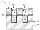
- H01L21/76897—Formation of self-aligned vias or contact plugs, i.e. involving a lithographically uncritical step
-
- H—ELECTRICITY
- H01—ELECTRIC ELEMENTS
- H01L—SEMICONDUCTOR DEVICES NOT COVERED BY CLASS H10
- H01L21/00—Processes or apparatus adapted for the manufacture or treatment of semiconductor or solid state devices or of parts thereof
- H01L21/02—Manufacture or treatment of semiconductor devices or of parts thereof
- H01L21/04—Manufacture or treatment of semiconductor devices or of parts thereof the devices having potential barriers, e.g. a PN junction, depletion layer or carrier concentration layer
- H01L21/18—Manufacture or treatment of semiconductor devices or of parts thereof the devices having potential barriers, e.g. a PN junction, depletion layer or carrier concentration layer the devices having semiconductor bodies comprising elements of Group IV of the Periodic Table or AIIIBV compounds with or without impurities, e.g. doping materials
- H01L21/30—Treatment of semiconductor bodies using processes or apparatus not provided for in groups H01L21/20 - H01L21/26
- H01L21/31—Treatment of semiconductor bodies using processes or apparatus not provided for in groups H01L21/20 - H01L21/26 to form insulating layers thereon, e.g. for masking or by using photolithographic techniques; After treatment of these layers; Selection of materials for these layers
- H01L21/32—Treatment of semiconductor bodies using processes or apparatus not provided for in groups H01L21/20 - H01L21/26 to form insulating layers thereon, e.g. for masking or by using photolithographic techniques; After treatment of these layers; Selection of materials for these layers using masks
-
- H—ELECTRICITY
- H01—ELECTRIC ELEMENTS
- H01L—SEMICONDUCTOR DEVICES NOT COVERED BY CLASS H10
- H01L21/00—Processes or apparatus adapted for the manufacture or treatment of semiconductor or solid state devices or of parts thereof
- H01L21/67—Apparatus specially adapted for handling semiconductor or electric solid state devices during manufacture or treatment thereof; Apparatus specially adapted for handling wafers during manufacture or treatment of semiconductor or electric solid state devices or components ; Apparatus not specifically provided for elsewhere
- H01L21/683—Apparatus specially adapted for handling semiconductor or electric solid state devices during manufacture or treatment thereof; Apparatus specially adapted for handling wafers during manufacture or treatment of semiconductor or electric solid state devices or components ; Apparatus not specifically provided for elsewhere for supporting or gripping
- H01L21/687—Apparatus specially adapted for handling semiconductor or electric solid state devices during manufacture or treatment thereof; Apparatus specially adapted for handling wafers during manufacture or treatment of semiconductor or electric solid state devices or components ; Apparatus not specifically provided for elsewhere for supporting or gripping using mechanical means, e.g. chucks, clamps or pinches
- H01L21/68714—Apparatus specially adapted for handling semiconductor or electric solid state devices during manufacture or treatment thereof; Apparatus specially adapted for handling wafers during manufacture or treatment of semiconductor or electric solid state devices or components ; Apparatus not specifically provided for elsewhere for supporting or gripping using mechanical means, e.g. chucks, clamps or pinches the wafers being placed on a susceptor, stage or support
- H01L21/68764—Apparatus specially adapted for handling semiconductor or electric solid state devices during manufacture or treatment thereof; Apparatus specially adapted for handling wafers during manufacture or treatment of semiconductor or electric solid state devices or components ; Apparatus not specifically provided for elsewhere for supporting or gripping using mechanical means, e.g. chucks, clamps or pinches the wafers being placed on a susceptor, stage or support characterised by a movable susceptor, stage or support, others than those only rotating on their own vertical axis, e.g. susceptors on a rotating caroussel
-
- H—ELECTRICITY
- H01—ELECTRIC ELEMENTS
- H01L—SEMICONDUCTOR DEVICES NOT COVERED BY CLASS H10
- H01L21/00—Processes or apparatus adapted for the manufacture or treatment of semiconductor or solid state devices or of parts thereof
- H01L21/67—Apparatus specially adapted for handling semiconductor or electric solid state devices during manufacture or treatment thereof; Apparatus specially adapted for handling wafers during manufacture or treatment of semiconductor or electric solid state devices or components ; Apparatus not specifically provided for elsewhere
- H01L21/683—Apparatus specially adapted for handling semiconductor or electric solid state devices during manufacture or treatment thereof; Apparatus specially adapted for handling wafers during manufacture or treatment of semiconductor or electric solid state devices or components ; Apparatus not specifically provided for elsewhere for supporting or gripping
- H01L21/687—Apparatus specially adapted for handling semiconductor or electric solid state devices during manufacture or treatment thereof; Apparatus specially adapted for handling wafers during manufacture or treatment of semiconductor or electric solid state devices or components ; Apparatus not specifically provided for elsewhere for supporting or gripping using mechanical means, e.g. chucks, clamps or pinches
- H01L21/68714—Apparatus specially adapted for handling semiconductor or electric solid state devices during manufacture or treatment thereof; Apparatus specially adapted for handling wafers during manufacture or treatment of semiconductor or electric solid state devices or components ; Apparatus not specifically provided for elsewhere for supporting or gripping using mechanical means, e.g. chucks, clamps or pinches the wafers being placed on a susceptor, stage or support
- H01L21/68771—Apparatus specially adapted for handling semiconductor or electric solid state devices during manufacture or treatment thereof; Apparatus specially adapted for handling wafers during manufacture or treatment of semiconductor or electric solid state devices or components ; Apparatus not specifically provided for elsewhere for supporting or gripping using mechanical means, e.g. chucks, clamps or pinches the wafers being placed on a susceptor, stage or support characterised by supporting more than one semiconductor substrate
Landscapes
- Engineering & Computer Science (AREA)
- Physics & Mathematics (AREA)
- General Physics & Mathematics (AREA)
- Power Engineering (AREA)
- Microelectronics & Electronic Packaging (AREA)
- Computer Hardware Design (AREA)
- Manufacturing & Machinery (AREA)
- Condensed Matter Physics & Semiconductors (AREA)
- Chemical & Material Sciences (AREA)
- Chemical Kinetics & Catalysis (AREA)
- Mechanical Engineering (AREA)
- Organic Chemistry (AREA)
- Metallurgy (AREA)
- Materials Engineering (AREA)
- General Chemical & Material Sciences (AREA)
- Plasma & Fusion (AREA)
- Spectroscopy & Molecular Physics (AREA)
- Robotics (AREA)
- Inorganic Chemistry (AREA)
- Chemical Vapour Deposition (AREA)
- Formation Of Insulating Films (AREA)
- Internal Circuitry In Semiconductor Integrated Circuit Devices (AREA)
- Electrodes Of Semiconductors (AREA)
Applications Claiming Priority (4)
| Application Number | Priority Date | Filing Date | Title |
|---|---|---|---|
| US201762588855P | 2017-11-20 | 2017-11-20 | |
| US62/588,855 | 2017-11-20 | ||
| US201862685847P | 2018-06-15 | 2018-06-15 | |
| US62/685,847 | 2018-06-15 |
Publications (2)
| Publication Number | Publication Date |
|---|---|
| KR20190058343A KR20190058343A (ko) | 2019-05-29 |
| KR102491746B1 true KR102491746B1 (ko) | 2023-01-25 |
Family
ID=66533236
Family Applications (3)
| Application Number | Title | Priority Date | Filing Date |
|---|---|---|---|
| KR1020180143517A Active KR102491746B1 (ko) | 2017-11-20 | 2018-11-20 | 완전히 자기 정렬된 비아를 형성하기 위한 선택적 막 퇴적 방법 |
| KR1020180143516A Active KR102523731B1 (ko) | 2017-11-20 | 2018-11-20 | 완전히 자기 정렬된 비아를 형성하기 위한 선택적 퇴적 방법 |
| KR1020220116934A Active KR102549289B1 (ko) | 2017-11-20 | 2022-09-16 | 완전히 자기 정렬된 비아를 형성하기 위한 선택적 퇴적 방법 |
Family Applications After (2)
| Application Number | Title | Priority Date | Filing Date |
|---|---|---|---|
| KR1020180143516A Active KR102523731B1 (ko) | 2017-11-20 | 2018-11-20 | 완전히 자기 정렬된 비아를 형성하기 위한 선택적 퇴적 방법 |
| KR1020220116934A Active KR102549289B1 (ko) | 2017-11-20 | 2022-09-16 | 완전히 자기 정렬된 비아를 형성하기 위한 선택적 퇴적 방법 |
Country Status (4)
| Country | Link |
|---|---|
| US (3) | US10847363B2 (enExample) |
| JP (2) | JP7287770B2 (enExample) |
| KR (3) | KR102491746B1 (enExample) |
| TW (2) | TWI788463B (enExample) |
Families Citing this family (55)
| Publication number | Priority date | Publication date | Assignee | Title |
|---|---|---|---|---|
| US9112003B2 (en) | 2011-12-09 | 2015-08-18 | Asm International N.V. | Selective formation of metallic films on metallic surfaces |
| TWI686499B (zh) | 2014-02-04 | 2020-03-01 | 荷蘭商Asm Ip控股公司 | 金屬、金屬氧化物與介電質的選擇性沉積 |
| US10047435B2 (en) | 2014-04-16 | 2018-08-14 | Asm Ip Holding B.V. | Dual selective deposition |
| US9490145B2 (en) | 2015-02-23 | 2016-11-08 | Asm Ip Holding B.V. | Removal of surface passivation |
| US10428421B2 (en) | 2015-08-03 | 2019-10-01 | Asm Ip Holding B.V. | Selective deposition on metal or metallic surfaces relative to dielectric surfaces |
| US10695794B2 (en) | 2015-10-09 | 2020-06-30 | Asm Ip Holding B.V. | Vapor phase deposition of organic films |
| US10814349B2 (en) | 2015-10-09 | 2020-10-27 | Asm Ip Holding B.V. | Vapor phase deposition of organic films |
| US11081342B2 (en) | 2016-05-05 | 2021-08-03 | Asm Ip Holding B.V. | Selective deposition using hydrophobic precursors |
| US10453701B2 (en) | 2016-06-01 | 2019-10-22 | Asm Ip Holding B.V. | Deposition of organic films |
| US10373820B2 (en) | 2016-06-01 | 2019-08-06 | Asm Ip Holding B.V. | Deposition of organic films |
| US11430656B2 (en) | 2016-11-29 | 2022-08-30 | Asm Ip Holding B.V. | Deposition of oxide thin films |
| JP7169072B2 (ja) | 2017-02-14 | 2022-11-10 | エーエスエム アイピー ホールディング ビー.ブイ. | 選択的パッシベーションおよび選択的堆積 |
| US11501965B2 (en) * | 2017-05-05 | 2022-11-15 | Asm Ip Holding B.V. | Plasma enhanced deposition processes for controlled formation of metal oxide thin films |
| KR102684628B1 (ko) | 2017-05-16 | 2024-07-15 | 에이에스엠 아이피 홀딩 비.브이. | 유전체 상에 옥사이드의 선택적 peald |
| US10847363B2 (en) | 2017-11-20 | 2020-11-24 | Tokyo Electron Limited | Method of selective deposition for forming fully self-aligned vias |
| TWI894126B (zh) * | 2018-04-27 | 2025-08-21 | 日商東京威力科創股份有限公司 | 用於先進接觸件中之覆蓋層形成的區域選擇性沉積 |
| US12482648B2 (en) | 2018-10-02 | 2025-11-25 | Asm Ip Holding B.V. | Selective passivation and selective deposition |
| JP2020056104A (ja) | 2018-10-02 | 2020-04-09 | エーエスエム アイピー ホールディング ビー.ブイ. | 選択的パッシベーションおよび選択的堆積 |
| SG11202110268WA (en) * | 2019-03-20 | 2021-10-28 | Kokusai Electric Corp | Method of manufacturing semiconductor device, method of processing substrate, substrate processing apparatus, and program |
| US11965238B2 (en) | 2019-04-12 | 2024-04-23 | Asm Ip Holding B.V. | Selective deposition of metal oxides on metal surfaces |
| TWI845699B (zh) | 2019-06-12 | 2024-06-21 | 日商東京威力科創股份有限公司 | 半導體裝置的平坦化 |
| JP7531981B2 (ja) * | 2019-07-18 | 2024-08-13 | 東京エレクトロン株式会社 | 領域選択的堆積における横方向のフィルム成長を緩和するための方法 |
| JP2021052069A (ja) * | 2019-09-24 | 2021-04-01 | 東京エレクトロン株式会社 | 成膜方法 |
| JP7262354B2 (ja) * | 2019-09-24 | 2023-04-21 | 東京エレクトロン株式会社 | 成膜方法 |
| JP2021057563A (ja) * | 2019-09-24 | 2021-04-08 | 東京エレクトロン株式会社 | 成膜方法 |
| US11139163B2 (en) | 2019-10-31 | 2021-10-05 | Asm Ip Holding B.V. | Selective deposition of SiOC thin films |
| US20210134669A1 (en) * | 2019-10-31 | 2021-05-06 | Taiwan Semiconductor Manufacturing Co., Ltd. | Isolation structure for metal interconnect |
| CN114830323A (zh) * | 2019-12-10 | 2022-07-29 | 东京毅力科创株式会社 | 作为牺牲覆盖层的自组装单层 |
| JP7365898B2 (ja) * | 2019-12-27 | 2023-10-20 | 東京エレクトロン株式会社 | 成膜方法及び成膜装置 |
| JP7227122B2 (ja) * | 2019-12-27 | 2023-02-21 | 株式会社Kokusai Electric | 基板処理方法、半導体装置の製造方法、基板処理装置、およびプログラム |
| JP7353200B2 (ja) * | 2020-02-06 | 2023-09-29 | 東京エレクトロン株式会社 | 成膜方法 |
| JP7072012B2 (ja) | 2020-02-27 | 2022-05-19 | 株式会社Kokusai Electric | 基板処理方法、半導体装置の製造方法、基板処理装置、及びプログラム |
| TW202140832A (zh) | 2020-03-30 | 2021-11-01 | 荷蘭商Asm Ip私人控股有限公司 | 氧化矽在金屬表面上之選擇性沉積 |
| TWI862807B (zh) | 2020-03-30 | 2024-11-21 | 荷蘭商Asm Ip私人控股有限公司 | 相對於金屬表面在介電表面上之氧化矽的選擇性沉積 |
| TWI865747B (zh) | 2020-03-30 | 2024-12-11 | 荷蘭商Asm Ip私人控股有限公司 | 在兩不同表面上同時選擇性沉積兩不同材料 |
| US11542597B2 (en) * | 2020-04-08 | 2023-01-03 | Applied Materials, Inc. | Selective deposition of metal oxide by pulsed chemical vapor deposition |
| US20210398846A1 (en) * | 2020-06-17 | 2021-12-23 | Tokyo Electron Limited | Method for area selective deposition using a surface cleaning process |
| JP2022050198A (ja) * | 2020-09-17 | 2022-03-30 | 東京エレクトロン株式会社 | 成膜方法及び成膜装置 |
| US20220136106A1 (en) * | 2020-10-30 | 2022-05-05 | The Board Of Trustees Of The Leland Stanford Junior University | Advanced precursors for selective atomic layer deposition using self-assembled monolayers |
| US20220238323A1 (en) * | 2021-01-28 | 2022-07-28 | Tokyo Electron Limited | Method for selective deposition of dielectric on dielectric |
| US20220254630A1 (en) * | 2021-02-08 | 2022-08-11 | Tokyo Electron Limited | Liquid phase conformal silicon oxide spin-on deposition |
| US20240194456A1 (en) * | 2021-03-31 | 2024-06-13 | Tokyo Electron Limited | Film forming method and substrate processing apparatus |
| JP2024523510A (ja) * | 2021-07-06 | 2024-06-28 | 東京エレクトロン株式会社 | 自己組織化単分子層を使用する選択的な膜形成 |
| JP2024546040A (ja) * | 2021-11-26 | 2024-12-17 | ソウルブレイン シーオー., エルティーディー. | 高誘電率薄膜用マスキング剤、それを利用した選択領域蒸着方法、それから製造された半導体基板及び半導体素子 |
| US20230282514A1 (en) * | 2022-03-04 | 2023-09-07 | Taiwan Semiconductor Manufacturing Company, Ltd. | Area selective deposition for zero via enclosure and extremely small metal line end space |
| EP4511869A1 (en) * | 2022-04-21 | 2025-02-26 | Gelest, Inc. | Inherent area selective deposition of mixed oxide dielectric film |
| JP2023182324A (ja) | 2022-06-14 | 2023-12-26 | 東京エレクトロン株式会社 | 成膜方法及び成膜装置 |
| JP2024019774A (ja) * | 2022-08-01 | 2024-02-14 | 東京エレクトロン株式会社 | 成膜方法および成膜装置 |
| CN115418629B (zh) * | 2022-08-17 | 2024-01-12 | 杭州富芯半导体有限公司 | 薄膜沉积的方法 |
| JP2024049188A (ja) * | 2022-09-28 | 2024-04-09 | 東京エレクトロン株式会社 | 膜形成方法及び基板処理装置 |
| JP2024081396A (ja) * | 2022-12-06 | 2024-06-18 | 東京エレクトロン株式会社 | 成膜方法及び成膜装置 |
| JP2024165284A (ja) * | 2023-05-17 | 2024-11-28 | 東京応化工業株式会社 | 表面処理膜の形成方法 |
| JP2025005618A (ja) * | 2023-06-28 | 2025-01-17 | 東京エレクトロン株式会社 | 成膜方法及び成膜装置 |
| US20250074927A1 (en) * | 2023-08-29 | 2025-03-06 | Entegris, Inc. | Precursors for selective deposition of silicon-containing films |
| JP2025087989A (ja) * | 2023-11-30 | 2025-06-11 | 東京エレクトロン株式会社 | 成膜方法及び成膜装置 |
Citations (7)
| Publication number | Priority date | Publication date | Assignee | Title |
|---|---|---|---|---|
| JP2005285821A (ja) | 2004-03-26 | 2005-10-13 | Fujitsu Ltd | 半導体装置およびその製造方法 |
| US20080032604A1 (en) | 2004-06-22 | 2008-02-07 | Martin Jose L | Servo Stroking Apparatus and System |
| KR101048900B1 (ko) | 2008-06-27 | 2011-07-12 | 도쿄엘렉트론가부시키가이샤 | 박막 증착 장치, 기판 처리 장치, 박막 증착 방법 및 컴퓨터로 판독 가능한 기억 매체 |
| JP2015149434A (ja) | 2014-02-07 | 2015-08-20 | ウシオ電機株式会社 | パターン形成体の製造方法 |
| US20160172189A1 (en) | 2014-12-15 | 2016-06-16 | Tokyo Electron Limited | Method of selective gas phase film deposition on a substrate |
| US20170029948A1 (en) | 2015-07-28 | 2017-02-02 | Asm Ip Holding B.V. | Methods and apparatuses for temperature-indexed thin film deposition |
| US20170294339A1 (en) | 2016-04-12 | 2017-10-12 | Tokyo Electron Limited | METHODS FOR SiO2 FILLING OF FINE RECESSED FEATURES AND SELECTIVE SiO2 DEPOSITION ON CATALYTIC SURFACES |
Family Cites Families (22)
| Publication number | Priority date | Publication date | Assignee | Title |
|---|---|---|---|---|
| JP3469251B2 (ja) * | 1990-02-14 | 2003-11-25 | 株式会社東芝 | 半導体装置の製造方法 |
| US20060073276A1 (en) * | 2004-10-04 | 2006-04-06 | Eric Antonissen | Multi-zone atomic layer deposition apparatus and method |
| WO2008008319A2 (en) | 2006-07-10 | 2008-01-17 | President And Fellows Of Harvard College | Selective sealing of porous dielectric materials |
| CN101646468A (zh) * | 2006-10-10 | 2010-02-10 | 西洛诺瓦生物科学公司 | 包含硅酮和特定聚磷氮烯的组合物和装置 |
| US9245739B2 (en) * | 2006-11-01 | 2016-01-26 | Lam Research Corporation | Low-K oxide deposition by hydrolysis and condensation |
| JP2010010686A (ja) * | 2008-06-27 | 2010-01-14 | Asm America Inc | 高成長率の二酸化ケイ素の堆積 |
| JP2010041038A (ja) * | 2008-06-27 | 2010-02-18 | Asm America Inc | 重要な用途のための二酸化ケイ素の低温熱でのald |
| US8907881B2 (en) * | 2010-04-09 | 2014-12-09 | Semiconductor Energy Laboratory Co., Ltd. | Liquid crystal display device and method for driving the same |
| WO2012083258A2 (en) * | 2010-12-16 | 2012-06-21 | Sensor Innovations, Inc. | Electrochemical sensors |
| JP2016536452A (ja) * | 2013-10-15 | 2016-11-24 | ビーコ・エーエルディー インコーポレイテッド | 種前駆体を用いる高速原子層堆積プロセス |
| TWI686499B (zh) | 2014-02-04 | 2020-03-01 | 荷蘭商Asm Ip控股公司 | 金屬、金屬氧化物與介電質的選擇性沉積 |
| GB201415119D0 (en) * | 2014-08-27 | 2014-10-08 | Ibm | Method for fabricating a semiconductor structure |
| US20160064275A1 (en) | 2014-08-27 | 2016-03-03 | Applied Materials, Inc. | Selective Deposition With Alcohol Selective Reduction And Protection |
| US9508545B2 (en) * | 2015-02-09 | 2016-11-29 | Applied Materials, Inc. | Selectively lateral growth of silicon oxide thin film |
| KR20170125876A (ko) * | 2015-02-26 | 2017-11-15 | 어플라이드 머티어리얼스, 인코포레이티드 | 자기-조립 단분자층들을 사용하는 선택적인 유전체 증착을 위한 방법들 |
| US20170092533A1 (en) * | 2015-09-29 | 2017-03-30 | Applied Materials, Inc. | Selective silicon dioxide deposition using phosphonic acid self assembled monolayers as nucleation inhibitor |
| US10316406B2 (en) * | 2015-10-21 | 2019-06-11 | Ultratech, Inc. | Methods of forming an ALD-inhibiting layer using a self-assembled monolayer |
| US9981286B2 (en) * | 2016-03-08 | 2018-05-29 | Asm Ip Holding B.V. | Selective formation of metal silicides |
| US10068764B2 (en) | 2016-09-13 | 2018-09-04 | Tokyo Electron Limited | Selective metal oxide deposition using a self-assembled monolayer surface pretreatment |
| US10453749B2 (en) | 2017-02-14 | 2019-10-22 | Tokyo Electron Limited | Method of forming a self-aligned contact using selective SiO2 deposition |
| US10847363B2 (en) | 2017-11-20 | 2020-11-24 | Tokyo Electron Limited | Method of selective deposition for forming fully self-aligned vias |
| US10468585B1 (en) * | 2018-05-31 | 2019-11-05 | International Business Machines Corporation | Dual function magnetic tunnel junction pillar encapsulation |
-
2018
- 2018-11-16 US US16/193,833 patent/US10847363B2/en active Active
- 2018-11-16 US US16/193,849 patent/US10586734B2/en active Active
- 2018-11-19 TW TW107141017A patent/TWI788463B/zh active
- 2018-11-19 TW TW107141020A patent/TWI798290B/zh active
- 2018-11-19 JP JP2018216745A patent/JP7287770B2/ja active Active
- 2018-11-20 KR KR1020180143517A patent/KR102491746B1/ko active Active
- 2018-11-20 KR KR1020180143516A patent/KR102523731B1/ko active Active
- 2018-11-20 JP JP2018217623A patent/JP7193990B2/ja active Active
-
2020
- 2020-11-23 US US17/102,054 patent/US11658068B2/en active Active
-
2022
- 2022-09-16 KR KR1020220116934A patent/KR102549289B1/ko active Active
Patent Citations (8)
| Publication number | Priority date | Publication date | Assignee | Title |
|---|---|---|---|---|
| JP2005285821A (ja) | 2004-03-26 | 2005-10-13 | Fujitsu Ltd | 半導体装置およびその製造方法 |
| US20080032604A1 (en) | 2004-06-22 | 2008-02-07 | Martin Jose L | Servo Stroking Apparatus and System |
| KR101048900B1 (ko) | 2008-06-27 | 2011-07-12 | 도쿄엘렉트론가부시키가이샤 | 박막 증착 장치, 기판 처리 장치, 박막 증착 방법 및 컴퓨터로 판독 가능한 기억 매체 |
| KR101533464B1 (ko) | 2008-06-27 | 2015-07-02 | 도쿄엘렉트론가부시키가이샤 | 박막 증착 장치, 박막 증착 방법 및 컴퓨터로 판독가능한 기억 매체 |
| JP2015149434A (ja) | 2014-02-07 | 2015-08-20 | ウシオ電機株式会社 | パターン形成体の製造方法 |
| US20160172189A1 (en) | 2014-12-15 | 2016-06-16 | Tokyo Electron Limited | Method of selective gas phase film deposition on a substrate |
| US20170029948A1 (en) | 2015-07-28 | 2017-02-02 | Asm Ip Holding B.V. | Methods and apparatuses for temperature-indexed thin film deposition |
| US20170294339A1 (en) | 2016-04-12 | 2017-10-12 | Tokyo Electron Limited | METHODS FOR SiO2 FILLING OF FINE RECESSED FEATURES AND SELECTIVE SiO2 DEPOSITION ON CATALYTIC SURFACES |
Also Published As
| Publication number | Publication date |
|---|---|
| TW201930625A (zh) | 2019-08-01 |
| TW202328473A (zh) | 2023-07-16 |
| US20190157149A1 (en) | 2019-05-23 |
| KR20220132493A (ko) | 2022-09-30 |
| US10847363B2 (en) | 2020-11-24 |
| US10586734B2 (en) | 2020-03-10 |
| KR20190058342A (ko) | 2019-05-29 |
| US20190164749A1 (en) | 2019-05-30 |
| JP2019096877A (ja) | 2019-06-20 |
| JP7193990B2 (ja) | 2022-12-21 |
| JP2019096881A (ja) | 2019-06-20 |
| KR102549289B1 (ko) | 2023-06-29 |
| US20210074584A1 (en) | 2021-03-11 |
| TW201930626A (zh) | 2019-08-01 |
| TWI788463B (zh) | 2023-01-01 |
| KR20190058343A (ko) | 2019-05-29 |
| JP7287770B2 (ja) | 2023-06-06 |
| US11658068B2 (en) | 2023-05-23 |
| KR102523731B1 (ko) | 2023-04-19 |
| TWI798290B (zh) | 2023-04-11 |
Similar Documents
| Publication | Publication Date | Title |
|---|---|---|
| KR102491746B1 (ko) | 완전히 자기 정렬된 비아를 형성하기 위한 선택적 막 퇴적 방법 | |
| US20250029840A1 (en) | Molybdenum deposition | |
| TWI755607B (zh) | 金屬薄膜之催化沉積 | |
| US12416080B2 (en) | Atomic layer self aligned substrate processing and integrated toolset | |
| KR102361468B1 (ko) | 핵형성을 사용하지 않는 갭 충전 ald 프로세스 | |
| TWI497592B (zh) | 成膜裝置及成膜方法 | |
| KR102469407B1 (ko) | 일괄 처리 시스템에서의 다중막 퇴적 및 에칭을 위한 방법 및 장치 | |
| TWI808049B (zh) | 處理基板的方法 | |
| US9136133B2 (en) | Method of depositing film | |
| JP4410497B2 (ja) | 成膜方法 | |
| JP2012195513A (ja) | プラズマ処理装置 | |
| TW201928108A (zh) | 釕的選擇性原子層沉積 | |
| KR20180036740A (ko) | 온도-인덱싱된 박막 증착을 위한 방법 및 장치 | |
| CN112514052A (zh) | 多层特征填充 | |
| KR20190037126A (ko) | 선택 성막 방법 및 반도체 장치의 제조 방법 | |
| JP5011355B2 (ja) | 成膜方法 | |
| TWI871373B (zh) | Pmos高k金屬閘極及製造金屬閘極疊層之方法 | |
| KR20180036694A (ko) | 박막 증착을 위한 방법 및 장치 | |
| US11664215B2 (en) | High selectivity atomic later deposition process | |
| CN112218975A (zh) | 减少跨膜界面的扩散 |
Legal Events
| Date | Code | Title | Description |
|---|---|---|---|
| PA0109 | Patent application |
Patent event code: PA01091R01D Comment text: Patent Application Patent event date: 20181120 |
|
| PG1501 | Laying open of application | ||
| PA0201 | Request for examination |
Patent event code: PA02012R01D Patent event date: 20201224 Comment text: Request for Examination of Application Patent event code: PA02011R01I Patent event date: 20181120 Comment text: Patent Application |
|
| E902 | Notification of reason for refusal | ||
| PE0902 | Notice of grounds for rejection |
Comment text: Notification of reason for refusal Patent event date: 20220728 Patent event code: PE09021S01D |
|
| E701 | Decision to grant or registration of patent right | ||
| PE0701 | Decision of registration |
Patent event code: PE07011S01D Comment text: Decision to Grant Registration Patent event date: 20230107 |
|
| GRNT | Written decision to grant | ||
| PR0701 | Registration of establishment |
Comment text: Registration of Establishment Patent event date: 20230119 Patent event code: PR07011E01D |
|
| PR1002 | Payment of registration fee |
Payment date: 20230119 End annual number: 3 Start annual number: 1 |
|
| PG1601 | Publication of registration |