JP7577671B2 - 半導体装置 - Google Patents
半導体装置 Download PDFInfo
- Publication number
- JP7577671B2 JP7577671B2 JP2021546060A JP2021546060A JP7577671B2 JP 7577671 B2 JP7577671 B2 JP 7577671B2 JP 2021546060 A JP2021546060 A JP 2021546060A JP 2021546060 A JP2021546060 A JP 2021546060A JP 7577671 B2 JP7577671 B2 JP 7577671B2
- Authority
- JP
- Japan
- Prior art keywords
- oxide
- insulator
- conductor
- transistor
- region
- Prior art date
- Legal status (The legal status is an assumption and is not a legal conclusion. Google has not performed a legal analysis and makes no representation as to the accuracy of the status listed.)
- Active
Links
- 239000004065 semiconductor Substances 0.000 title claims description 214
- 230000006870 function Effects 0.000 claims description 164
- 230000015654 memory Effects 0.000 claims description 133
- 229910044991 metal oxide Inorganic materials 0.000 claims description 124
- 150000004706 metal oxides Chemical class 0.000 claims description 124
- 239000011701 zinc Substances 0.000 claims description 48
- 238000000034 method Methods 0.000 claims description 40
- 230000015572 biosynthetic process Effects 0.000 claims description 38
- 230000008569 process Effects 0.000 claims description 16
- 238000004364 calculation method Methods 0.000 claims description 13
- 229910052738 indium Inorganic materials 0.000 claims description 10
- APFVFJFRJDLVQX-UHFFFAOYSA-N indium atom Chemical compound [In] APFVFJFRJDLVQX-UHFFFAOYSA-N 0.000 claims description 8
- 239000011159 matrix material Substances 0.000 claims description 6
- 229910052725 zinc Inorganic materials 0.000 claims description 5
- HCHKCACWOHOZIP-UHFFFAOYSA-N Zinc Chemical compound [Zn] HCHKCACWOHOZIP-UHFFFAOYSA-N 0.000 claims description 3
- 239000012212 insulator Substances 0.000 description 476
- 239000004020 conductor Substances 0.000 description 470
- 239000010408 film Substances 0.000 description 158
- 239000010410 layer Substances 0.000 description 146
- 210000004027 cell Anatomy 0.000 description 124
- 229910052760 oxygen Inorganic materials 0.000 description 120
- 239000001301 oxygen Substances 0.000 description 119
- QVGXLLKOCUKJST-UHFFFAOYSA-N atomic oxygen Chemical compound [O] QVGXLLKOCUKJST-UHFFFAOYSA-N 0.000 description 118
- 239000001257 hydrogen Substances 0.000 description 108
- 229910052739 hydrogen Inorganic materials 0.000 description 108
- UFHFLCQGNIYNRP-UHFFFAOYSA-N Hydrogen Chemical compound [H][H] UFHFLCQGNIYNRP-UHFFFAOYSA-N 0.000 description 86
- 239000000463 material Substances 0.000 description 79
- 239000012535 impurity Substances 0.000 description 68
- 230000004888 barrier function Effects 0.000 description 59
- 238000009792 diffusion process Methods 0.000 description 53
- 229910052782 aluminium Inorganic materials 0.000 description 41
- XAGFODPZIPBFFR-UHFFFAOYSA-N aluminium Chemical compound [Al] XAGFODPZIPBFFR-UHFFFAOYSA-N 0.000 description 40
- 239000013078 crystal Substances 0.000 description 39
- 239000000758 substrate Substances 0.000 description 38
- VYPSYNLAJGMNEJ-UHFFFAOYSA-N Silicium dioxide Chemical compound O=[Si]=O VYPSYNLAJGMNEJ-UHFFFAOYSA-N 0.000 description 36
- 229910052814 silicon oxide Inorganic materials 0.000 description 36
- XUIMIQQOPSSXEZ-UHFFFAOYSA-N Silicon Chemical compound [Si] XUIMIQQOPSSXEZ-UHFFFAOYSA-N 0.000 description 35
- 229910052710 silicon Inorganic materials 0.000 description 34
- 239000010703 silicon Substances 0.000 description 34
- 229910052721 tungsten Inorganic materials 0.000 description 31
- 239000010937 tungsten Substances 0.000 description 31
- 125000004429 atom Chemical group 0.000 description 30
- WFKWXMTUELFFGS-UHFFFAOYSA-N tungsten Chemical compound [W] WFKWXMTUELFFGS-UHFFFAOYSA-N 0.000 description 30
- XLYOFNOQVPJJNP-UHFFFAOYSA-N water Substances O XLYOFNOQVPJJNP-UHFFFAOYSA-N 0.000 description 30
- 229910001868 water Inorganic materials 0.000 description 30
- IJGRMHOSHXDMSA-UHFFFAOYSA-N Atomic nitrogen Chemical compound N#N IJGRMHOSHXDMSA-UHFFFAOYSA-N 0.000 description 28
- 229910052581 Si3N4 Inorganic materials 0.000 description 28
- TWNQGVIAIRXVLR-UHFFFAOYSA-N oxo(oxoalumanyloxy)alumane Chemical compound O=[Al]O[Al]=O TWNQGVIAIRXVLR-UHFFFAOYSA-N 0.000 description 28
- HQVNEWCFYHHQES-UHFFFAOYSA-N silicon nitride Chemical compound N12[Si]34N5[Si]62N3[Si]51N64 HQVNEWCFYHHQES-UHFFFAOYSA-N 0.000 description 28
- 229910052751 metal Inorganic materials 0.000 description 26
- 210000002569 neuron Anatomy 0.000 description 25
- 229910052735 hafnium Inorganic materials 0.000 description 24
- RYGMFSIKBFXOCR-UHFFFAOYSA-N Copper Chemical compound [Cu] RYGMFSIKBFXOCR-UHFFFAOYSA-N 0.000 description 23
- PXHVJJICTQNCMI-UHFFFAOYSA-N Nickel Chemical compound [Ni] PXHVJJICTQNCMI-UHFFFAOYSA-N 0.000 description 22
- 239000003990 capacitor Substances 0.000 description 22
- 150000002431 hydrogen Chemical class 0.000 description 22
- 230000007547 defect Effects 0.000 description 21
- RTAQQCXQSZGOHL-UHFFFAOYSA-N Titanium Chemical compound [Ti] RTAQQCXQSZGOHL-UHFFFAOYSA-N 0.000 description 20
- 239000002184 metal Substances 0.000 description 20
- 229910052719 titanium Inorganic materials 0.000 description 20
- 239000010936 titanium Substances 0.000 description 20
- 239000010949 copper Substances 0.000 description 19
- 229910052802 copper Inorganic materials 0.000 description 18
- -1 oxygen ions Chemical class 0.000 description 18
- 239000002356 single layer Substances 0.000 description 18
- 238000010586 diagram Methods 0.000 description 17
- 238000013528 artificial neural network Methods 0.000 description 16
- VBJZVLUMGGDVMO-UHFFFAOYSA-N hafnium atom Chemical compound [Hf] VBJZVLUMGGDVMO-UHFFFAOYSA-N 0.000 description 16
- 229910000449 hafnium oxide Inorganic materials 0.000 description 14
- WIHZLLGSGQNAGK-UHFFFAOYSA-N hafnium(4+);oxygen(2-) Chemical compound [O-2].[O-2].[Hf+4] WIHZLLGSGQNAGK-UHFFFAOYSA-N 0.000 description 14
- 229910052757 nitrogen Inorganic materials 0.000 description 14
- ZOKXTWBITQBERF-UHFFFAOYSA-N Molybdenum Chemical compound [Mo] ZOKXTWBITQBERF-UHFFFAOYSA-N 0.000 description 12
- 239000011229 interlayer Substances 0.000 description 12
- 229910052750 molybdenum Inorganic materials 0.000 description 12
- 239000011733 molybdenum Substances 0.000 description 12
- 230000002093 peripheral effect Effects 0.000 description 12
- 229910052715 tantalum Inorganic materials 0.000 description 12
- GUVRBAGPIYLISA-UHFFFAOYSA-N tantalum atom Chemical compound [Ta] GUVRBAGPIYLISA-UHFFFAOYSA-N 0.000 description 12
- MZLGASXMSKOWSE-UHFFFAOYSA-N tantalum nitride Chemical compound [Ta]#N MZLGASXMSKOWSE-UHFFFAOYSA-N 0.000 description 12
- NRTOMJZYCJJWKI-UHFFFAOYSA-N Titanium nitride Chemical compound [Ti]#N NRTOMJZYCJJWKI-UHFFFAOYSA-N 0.000 description 11
- 238000002441 X-ray diffraction Methods 0.000 description 11
- 230000005684 electric field Effects 0.000 description 11
- 238000010894 electron beam technology Methods 0.000 description 11
- 229910052759 nickel Inorganic materials 0.000 description 11
- 230000003647 oxidation Effects 0.000 description 11
- 238000007254 oxidation reaction Methods 0.000 description 11
- OKTJSMMVPCPJKN-UHFFFAOYSA-N Carbon Chemical compound [C] OKTJSMMVPCPJKN-UHFFFAOYSA-N 0.000 description 10
- 229910052733 gallium Inorganic materials 0.000 description 10
- 238000010438 heat treatment Methods 0.000 description 10
- 238000004519 manufacturing process Methods 0.000 description 10
- 150000004767 nitrides Chemical class 0.000 description 10
- 229910052799 carbon Inorganic materials 0.000 description 9
- 125000004430 oxygen atom Chemical group O* 0.000 description 9
- XEEYBQQBJWHFJM-UHFFFAOYSA-N Iron Chemical compound [Fe] XEEYBQQBJWHFJM-UHFFFAOYSA-N 0.000 description 8
- 239000000969 carrier Substances 0.000 description 8
- AJNVQOSZGJRYEI-UHFFFAOYSA-N digallium;oxygen(2-) Chemical compound [O-2].[O-2].[O-2].[Ga+3].[Ga+3] AJNVQOSZGJRYEI-UHFFFAOYSA-N 0.000 description 8
- 229910001195 gallium oxide Inorganic materials 0.000 description 8
- 229910052732 germanium Inorganic materials 0.000 description 8
- GNPVGFCGXDBREM-UHFFFAOYSA-N germanium atom Chemical compound [Ge] GNPVGFCGXDBREM-UHFFFAOYSA-N 0.000 description 8
- 230000003071 parasitic effect Effects 0.000 description 8
- 238000004544 sputter deposition Methods 0.000 description 8
- 229910052727 yttrium Inorganic materials 0.000 description 8
- ZOXJGFHDIHLPTG-UHFFFAOYSA-N Boron Chemical compound [B] ZOXJGFHDIHLPTG-UHFFFAOYSA-N 0.000 description 7
- GYHNNYVSQQEPJS-UHFFFAOYSA-N Gallium Chemical compound [Ga] GYHNNYVSQQEPJS-UHFFFAOYSA-N 0.000 description 7
- QCWXUUIWCKQGHC-UHFFFAOYSA-N Zirconium Chemical compound [Zr] QCWXUUIWCKQGHC-UHFFFAOYSA-N 0.000 description 7
- 239000000956 alloy Substances 0.000 description 7
- 238000004458 analytical method Methods 0.000 description 7
- 238000013473 artificial intelligence Methods 0.000 description 7
- 229910052796 boron Inorganic materials 0.000 description 7
- 239000000470 constituent Substances 0.000 description 7
- 230000000694 effects Effects 0.000 description 7
- 125000004435 hydrogen atom Chemical group [H]* 0.000 description 7
- 239000011810 insulating material Substances 0.000 description 7
- 239000007769 metal material Substances 0.000 description 7
- 239000000203 mixture Substances 0.000 description 7
- BPUBBGLMJRNUCC-UHFFFAOYSA-N oxygen(2-);tantalum(5+) Chemical compound [O-2].[O-2].[O-2].[O-2].[O-2].[Ta+5].[Ta+5] BPUBBGLMJRNUCC-UHFFFAOYSA-N 0.000 description 7
- RVTZCBVAJQQJTK-UHFFFAOYSA-N oxygen(2-);zirconium(4+) Chemical compound [O-2].[O-2].[Zr+4] RVTZCBVAJQQJTK-UHFFFAOYSA-N 0.000 description 7
- 229910052707 ruthenium Inorganic materials 0.000 description 7
- 238000001228 spectrum Methods 0.000 description 7
- 229910001936 tantalum oxide Inorganic materials 0.000 description 7
- VWQVUPCCIRVNHF-UHFFFAOYSA-N yttrium atom Chemical compound [Y] VWQVUPCCIRVNHF-UHFFFAOYSA-N 0.000 description 7
- 229910052726 zirconium Inorganic materials 0.000 description 7
- 229910001928 zirconium oxide Inorganic materials 0.000 description 7
- FYYHWMGAXLPEAU-UHFFFAOYSA-N Magnesium Chemical compound [Mg] FYYHWMGAXLPEAU-UHFFFAOYSA-N 0.000 description 6
- 238000005229 chemical vapour deposition Methods 0.000 description 6
- 229910052451 lead zirconate titanate Inorganic materials 0.000 description 6
- 229910052749 magnesium Inorganic materials 0.000 description 6
- 239000011777 magnesium Substances 0.000 description 6
- 239000013081 microcrystal Substances 0.000 description 6
- 229910021421 monocrystalline silicon Inorganic materials 0.000 description 6
- 239000012466 permeate Substances 0.000 description 6
- OGIDPMRJRNCKJF-UHFFFAOYSA-N titanium oxide Inorganic materials [Ti]=O OGIDPMRJRNCKJF-UHFFFAOYSA-N 0.000 description 6
- OAICVXFJPJFONN-UHFFFAOYSA-N Phosphorus Chemical compound [P] OAICVXFJPJFONN-UHFFFAOYSA-N 0.000 description 5
- KJTLSVCANCCWHF-UHFFFAOYSA-N Ruthenium Chemical compound [Ru] KJTLSVCANCCWHF-UHFFFAOYSA-N 0.000 description 5
- 229910052783 alkali metal Inorganic materials 0.000 description 5
- 150000001340 alkali metals Chemical class 0.000 description 5
- 229910052784 alkaline earth metal Inorganic materials 0.000 description 5
- 150000001342 alkaline earth metals Chemical class 0.000 description 5
- PMHQVHHXPFUNSP-UHFFFAOYSA-M copper(1+);methylsulfanylmethane;bromide Chemical compound Br[Cu].CSC PMHQVHHXPFUNSP-UHFFFAOYSA-M 0.000 description 5
- 238000007667 floating Methods 0.000 description 5
- 238000005468 ion implantation Methods 0.000 description 5
- 229910052746 lanthanum Inorganic materials 0.000 description 5
- FZLIPJUXYLNCLC-UHFFFAOYSA-N lanthanum atom Chemical compound [La] FZLIPJUXYLNCLC-UHFFFAOYSA-N 0.000 description 5
- 239000002159 nanocrystal Substances 0.000 description 5
- 229910052698 phosphorus Inorganic materials 0.000 description 5
- 239000011574 phosphorus Substances 0.000 description 5
- 238000012545 processing Methods 0.000 description 5
- 239000000047 product Substances 0.000 description 5
- 238000001004 secondary ion mass spectrometry Methods 0.000 description 5
- 238000003860 storage Methods 0.000 description 5
- 229910052712 strontium Inorganic materials 0.000 description 5
- JBRZTFJDHDCESZ-UHFFFAOYSA-N AsGa Chemical compound [As]#[Ga] JBRZTFJDHDCESZ-UHFFFAOYSA-N 0.000 description 4
- PXGOKWXKJXAPGV-UHFFFAOYSA-N Fluorine Chemical compound FF PXGOKWXKJXAPGV-UHFFFAOYSA-N 0.000 description 4
- 229910001218 Gallium arsenide Inorganic materials 0.000 description 4
- GWEVSGVZZGPLCZ-UHFFFAOYSA-N Titan oxide Chemical compound O=[Ti]=O GWEVSGVZZGPLCZ-UHFFFAOYSA-N 0.000 description 4
- XLOMVQKBTHCTTD-UHFFFAOYSA-N Zinc monoxide Chemical compound [Zn]=O XLOMVQKBTHCTTD-UHFFFAOYSA-N 0.000 description 4
- GPBUGPUPKAGMDK-UHFFFAOYSA-N azanylidynemolybdenum Chemical compound [Mo]#N GPBUGPUPKAGMDK-UHFFFAOYSA-N 0.000 description 4
- 150000004770 chalcogenides Chemical class 0.000 description 4
- 230000008859 change Effects 0.000 description 4
- 230000003247 decreasing effect Effects 0.000 description 4
- 229910052731 fluorine Inorganic materials 0.000 description 4
- 239000011737 fluorine Substances 0.000 description 4
- 239000007789 gas Substances 0.000 description 4
- YBMRDBCBODYGJE-UHFFFAOYSA-N germanium oxide Inorganic materials O=[Ge]=O YBMRDBCBODYGJE-UHFFFAOYSA-N 0.000 description 4
- 238000001341 grazing-angle X-ray diffraction Methods 0.000 description 4
- 229910003437 indium oxide Inorganic materials 0.000 description 4
- PJXISJQVUVHSOJ-UHFFFAOYSA-N indium(iii) oxide Chemical compound [O-2].[O-2].[O-2].[In+3].[In+3] PJXISJQVUVHSOJ-UHFFFAOYSA-N 0.000 description 4
- 229910052742 iron Inorganic materials 0.000 description 4
- MRELNEQAGSRDBK-UHFFFAOYSA-N lanthanum(3+);oxygen(2-) Chemical compound [O-2].[O-2].[O-2].[La+3].[La+3] MRELNEQAGSRDBK-UHFFFAOYSA-N 0.000 description 4
- 238000005259 measurement Methods 0.000 description 4
- PLDDOISOJJCEMH-UHFFFAOYSA-N neodymium(3+);oxygen(2-) Chemical compound [O-2].[O-2].[O-2].[Nd+3].[Nd+3] PLDDOISOJJCEMH-UHFFFAOYSA-N 0.000 description 4
- QGLKJKCYBOYXKC-UHFFFAOYSA-N nonaoxidotritungsten Chemical compound O=[W]1(=O)O[W](=O)(=O)O[W](=O)(=O)O1 QGLKJKCYBOYXKC-UHFFFAOYSA-N 0.000 description 4
- 238000010606 normalization Methods 0.000 description 4
- SIWVEOZUMHYXCS-UHFFFAOYSA-N oxo(oxoyttriooxy)yttrium Chemical compound O=[Y]O[Y]=O SIWVEOZUMHYXCS-UHFFFAOYSA-N 0.000 description 4
- PVADDRMAFCOOPC-UHFFFAOYSA-N oxogermanium Chemical compound [Ge]=O PVADDRMAFCOOPC-UHFFFAOYSA-N 0.000 description 4
- 229910001925 ruthenium oxide Inorganic materials 0.000 description 4
- WOCIAKWEIIZHES-UHFFFAOYSA-N ruthenium(iv) oxide Chemical compound O=[Ru]=O WOCIAKWEIIZHES-UHFFFAOYSA-N 0.000 description 4
- 239000000523 sample Substances 0.000 description 4
- 239000000126 substance Substances 0.000 description 4
- 239000010409 thin film Substances 0.000 description 4
- 238000012546 transfer Methods 0.000 description 4
- 229910001930 tungsten oxide Inorganic materials 0.000 description 4
- VYZAMTAEIAYCRO-UHFFFAOYSA-N Chromium Chemical compound [Cr] VYZAMTAEIAYCRO-UHFFFAOYSA-N 0.000 description 3
- 229910052779 Neodymium Inorganic materials 0.000 description 3
- MWUXSHHQAYIFBG-UHFFFAOYSA-N Nitric oxide Chemical compound O=[N] MWUXSHHQAYIFBG-UHFFFAOYSA-N 0.000 description 3
- 230000009471 action Effects 0.000 description 3
- 229910045601 alloy Inorganic materials 0.000 description 3
- 229910052804 chromium Inorganic materials 0.000 description 3
- 239000011651 chromium Substances 0.000 description 3
- 150000001875 compounds Chemical class 0.000 description 3
- 238000003795 desorption Methods 0.000 description 3
- 238000002149 energy-dispersive X-ray emission spectroscopy Methods 0.000 description 3
- 230000005669 field effect Effects 0.000 description 3
- 230000014509 gene expression Effects 0.000 description 3
- AMGQUBHHOARCQH-UHFFFAOYSA-N indium;oxotin Chemical compound [In].[Sn]=O AMGQUBHHOARCQH-UHFFFAOYSA-N 0.000 description 3
- HFGPZNIAWCZYJU-UHFFFAOYSA-N lead zirconate titanate Chemical compound [O-2].[O-2].[O-2].[O-2].[O-2].[Ti+4].[Zr+4].[Pb+2] HFGPZNIAWCZYJU-UHFFFAOYSA-N 0.000 description 3
- 238000002844 melting Methods 0.000 description 3
- 230000008018 melting Effects 0.000 description 3
- QEFYFXOXNSNQGX-UHFFFAOYSA-N neodymium atom Chemical compound [Nd] QEFYFXOXNSNQGX-UHFFFAOYSA-N 0.000 description 3
- CIOAGBVUUVVLOB-UHFFFAOYSA-N strontium atom Chemical compound [Sr] CIOAGBVUUVVLOB-UHFFFAOYSA-N 0.000 description 3
- VEALVRVVWBQVSL-UHFFFAOYSA-N strontium titanate Chemical compound [Sr+2].[O-][Ti]([O-])=O VEALVRVVWBQVSL-UHFFFAOYSA-N 0.000 description 3
- 229910052714 tellurium Inorganic materials 0.000 description 3
- PORWMNRCUJJQNO-UHFFFAOYSA-N tellurium atom Chemical compound [Te] PORWMNRCUJJQNO-UHFFFAOYSA-N 0.000 description 3
- 229910052718 tin Inorganic materials 0.000 description 3
- 229910052723 transition metal Inorganic materials 0.000 description 3
- YVTHLONGBIQYBO-UHFFFAOYSA-N zinc indium(3+) oxygen(2-) Chemical compound [O--].[Zn++].[In+3] YVTHLONGBIQYBO-UHFFFAOYSA-N 0.000 description 3
- XKRFYHLGVUSROY-UHFFFAOYSA-N Argon Chemical compound [Ar] XKRFYHLGVUSROY-UHFFFAOYSA-N 0.000 description 2
- 229910052684 Cerium Inorganic materials 0.000 description 2
- JMASRVWKEDWRBT-UHFFFAOYSA-N Gallium nitride Chemical compound [Ga]#N JMASRVWKEDWRBT-UHFFFAOYSA-N 0.000 description 2
- 229910000577 Silicon-germanium Inorganic materials 0.000 description 2
- BQCADISMDOOEFD-UHFFFAOYSA-N Silver Chemical compound [Ag] BQCADISMDOOEFD-UHFFFAOYSA-N 0.000 description 2
- NINIDFKCEFEMDL-UHFFFAOYSA-N Sulfur Chemical compound [S] NINIDFKCEFEMDL-UHFFFAOYSA-N 0.000 description 2
- ATJFFYVFTNAWJD-UHFFFAOYSA-N Tin Chemical compound [Sn] ATJFFYVFTNAWJD-UHFFFAOYSA-N 0.000 description 2
- 229910052785 arsenic Inorganic materials 0.000 description 2
- RQNWIZPPADIBDY-UHFFFAOYSA-N arsenic atom Chemical compound [As] RQNWIZPPADIBDY-UHFFFAOYSA-N 0.000 description 2
- 238000000231 atomic layer deposition Methods 0.000 description 2
- 229910052788 barium Inorganic materials 0.000 description 2
- 229910052790 beryllium Inorganic materials 0.000 description 2
- ATBAMAFKBVZNFJ-UHFFFAOYSA-N beryllium atom Chemical compound [Be] ATBAMAFKBVZNFJ-UHFFFAOYSA-N 0.000 description 2
- 230000005540 biological transmission Effects 0.000 description 2
- 229910000416 bismuth oxide Inorganic materials 0.000 description 2
- 230000000903 blocking effect Effects 0.000 description 2
- ZMIGMASIKSOYAM-UHFFFAOYSA-N cerium Chemical compound [Ce][Ce][Ce][Ce][Ce][Ce][Ce][Ce][Ce][Ce][Ce][Ce][Ce][Ce][Ce][Ce][Ce][Ce][Ce][Ce][Ce][Ce][Ce][Ce][Ce][Ce][Ce][Ce][Ce][Ce][Ce][Ce][Ce][Ce][Ce][Ce][Ce][Ce] ZMIGMASIKSOYAM-UHFFFAOYSA-N 0.000 description 2
- 229910052798 chalcogen Inorganic materials 0.000 description 2
- 150000001787 chalcogens Chemical class 0.000 description 2
- 230000000295 complement effect Effects 0.000 description 2
- 239000002131 composite material Substances 0.000 description 2
- 230000006866 deterioration Effects 0.000 description 2
- TYIXMATWDRGMPF-UHFFFAOYSA-N dibismuth;oxygen(2-) Chemical compound [O-2].[O-2].[O-2].[Bi+3].[Bi+3] TYIXMATWDRGMPF-UHFFFAOYSA-N 0.000 description 2
- 238000002003 electron diffraction Methods 0.000 description 2
- 238000002524 electron diffraction data Methods 0.000 description 2
- 238000000605 extraction Methods 0.000 description 2
- 238000007654 immersion Methods 0.000 description 2
- 150000002500 ions Chemical class 0.000 description 2
- CPLXHLVBOLITMK-UHFFFAOYSA-N magnesium oxide Inorganic materials [Mg]=O CPLXHLVBOLITMK-UHFFFAOYSA-N 0.000 description 2
- 239000000395 magnesium oxide Substances 0.000 description 2
- AXZKOIWUVFPNLO-UHFFFAOYSA-N magnesium;oxygen(2-) Chemical compound [O-2].[Mg+2] AXZKOIWUVFPNLO-UHFFFAOYSA-N 0.000 description 2
- 229910000484 niobium oxide Inorganic materials 0.000 description 2
- URLJKFSTXLNXLG-UHFFFAOYSA-N niobium(5+);oxygen(2-) Chemical compound [O-2].[O-2].[O-2].[O-2].[O-2].[Nb+5].[Nb+5] URLJKFSTXLNXLG-UHFFFAOYSA-N 0.000 description 2
- 230000001151 other effect Effects 0.000 description 2
- 230000001590 oxidative effect Effects 0.000 description 2
- 230000000737 periodic effect Effects 0.000 description 2
- BASFCYQUMIYNBI-UHFFFAOYSA-N platinum Chemical compound [Pt] BASFCYQUMIYNBI-UHFFFAOYSA-N 0.000 description 2
- 230000001681 protective effect Effects 0.000 description 2
- 239000011347 resin Substances 0.000 description 2
- 229920005989 resin Polymers 0.000 description 2
- HBMJWWWQQXIZIP-UHFFFAOYSA-N silicon carbide Chemical compound [Si+]#[C-] HBMJWWWQQXIZIP-UHFFFAOYSA-N 0.000 description 2
- 229910010271 silicon carbide Inorganic materials 0.000 description 2
- 229910052709 silver Inorganic materials 0.000 description 2
- 239000004332 silver Substances 0.000 description 2
- 239000011593 sulfur Substances 0.000 description 2
- 229910052717 sulfur Inorganic materials 0.000 description 2
- JBQYATWDVHIOAR-UHFFFAOYSA-N tellanylidenegermanium Chemical compound [Te]=[Ge] JBQYATWDVHIOAR-UHFFFAOYSA-N 0.000 description 2
- 229910052720 vanadium Inorganic materials 0.000 description 2
- GPPXJZIENCGNKB-UHFFFAOYSA-N vanadium Chemical compound [V]#[V] GPPXJZIENCGNKB-UHFFFAOYSA-N 0.000 description 2
- 239000011787 zinc oxide Substances 0.000 description 2
- 229910019311 (Ba,Sr)TiO Inorganic materials 0.000 description 1
- SDDGNMXIOGQCCH-UHFFFAOYSA-N 3-fluoro-n,n-dimethylaniline Chemical compound CN(C)C1=CC=CC(F)=C1 SDDGNMXIOGQCCH-UHFFFAOYSA-N 0.000 description 1
- 229910000838 Al alloy Inorganic materials 0.000 description 1
- ZAMOUSCENKQFHK-UHFFFAOYSA-N Chlorine atom Chemical compound [Cl] ZAMOUSCENKQFHK-UHFFFAOYSA-N 0.000 description 1
- 229910002601 GaN Inorganic materials 0.000 description 1
- 229910016001 MoSe Inorganic materials 0.000 description 1
- BUGBHKTXTAQXES-UHFFFAOYSA-N Selenium Chemical compound [Se] BUGBHKTXTAQXES-UHFFFAOYSA-N 0.000 description 1
- 238000005411 Van der Waals force Methods 0.000 description 1
- LEVVHYCKPQWKOP-UHFFFAOYSA-N [Si].[Ge] Chemical compound [Si].[Ge] LEVVHYCKPQWKOP-UHFFFAOYSA-N 0.000 description 1
- 238000009825 accumulation Methods 0.000 description 1
- 230000003213 activating effect Effects 0.000 description 1
- 230000004913 activation Effects 0.000 description 1
- UQZIWOQVLUASCR-UHFFFAOYSA-N alumane;titanium Chemical compound [AlH3].[Ti] UQZIWOQVLUASCR-UHFFFAOYSA-N 0.000 description 1
- MDPILPRLPQYEEN-UHFFFAOYSA-N aluminium arsenide Chemical compound [As]#[Al] MDPILPRLPQYEEN-UHFFFAOYSA-N 0.000 description 1
- 229910052786 argon Inorganic materials 0.000 description 1
- 230000006399 behavior Effects 0.000 description 1
- LNMGXZOOXVAITI-UHFFFAOYSA-N bis(selanylidene)hafnium Chemical compound [Se]=[Hf]=[Se] LNMGXZOOXVAITI-UHFFFAOYSA-N 0.000 description 1
- WVMYSOZCZHQCSG-UHFFFAOYSA-N bis(sulfanylidene)zirconium Chemical compound S=[Zr]=S WVMYSOZCZHQCSG-UHFFFAOYSA-N 0.000 description 1
- 238000006243 chemical reaction Methods 0.000 description 1
- 229910052801 chlorine Inorganic materials 0.000 description 1
- 239000000460 chlorine Substances 0.000 description 1
- 229910017052 cobalt Inorganic materials 0.000 description 1
- 239000010941 cobalt Substances 0.000 description 1
- GUTLYIVDDKVIGB-UHFFFAOYSA-N cobalt atom Chemical compound [Co] GUTLYIVDDKVIGB-UHFFFAOYSA-N 0.000 description 1
- 238000013135 deep learning Methods 0.000 description 1
- 230000001066 destructive effect Effects 0.000 description 1
- 238000001514 detection method Methods 0.000 description 1
- 238000011161 development Methods 0.000 description 1
- 229910003460 diamond Inorganic materials 0.000 description 1
- 239000010432 diamond Substances 0.000 description 1
- 238000009826 distribution Methods 0.000 description 1
- 238000005516 engineering process Methods 0.000 description 1
- 238000005530 etching Methods 0.000 description 1
- 230000005284 excitation Effects 0.000 description 1
- 239000000284 extract Substances 0.000 description 1
- 238000010304 firing Methods 0.000 description 1
- PCHJSUWPFVWCPO-UHFFFAOYSA-N gold Chemical compound [Au] PCHJSUWPFVWCPO-UHFFFAOYSA-N 0.000 description 1
- 229910052737 gold Inorganic materials 0.000 description 1
- 239000010931 gold Substances 0.000 description 1
- 229910021389 graphene Inorganic materials 0.000 description 1
- NRJVMVHUISHHQB-UHFFFAOYSA-N hafnium(4+);disulfide Chemical compound [S-2].[S-2].[Hf+4] NRJVMVHUISHHQB-UHFFFAOYSA-N 0.000 description 1
- 125000005843 halogen group Chemical group 0.000 description 1
- 239000001307 helium Substances 0.000 description 1
- 229910052734 helium Inorganic materials 0.000 description 1
- SWQJXJOGLNCZEY-UHFFFAOYSA-N helium atom Chemical compound [He] SWQJXJOGLNCZEY-UHFFFAOYSA-N 0.000 description 1
- 238000002173 high-resolution transmission electron microscopy Methods 0.000 description 1
- GPRLSGONYQIRFK-UHFFFAOYSA-N hydron Chemical compound [H+] GPRLSGONYQIRFK-UHFFFAOYSA-N 0.000 description 1
- 238000003384 imaging method Methods 0.000 description 1
- 230000006872 improvement Effects 0.000 description 1
- 230000010354 integration Effects 0.000 description 1
- 229910052741 iridium Inorganic materials 0.000 description 1
- GKOZUEZYRPOHIO-UHFFFAOYSA-N iridium atom Chemical compound [Ir] GKOZUEZYRPOHIO-UHFFFAOYSA-N 0.000 description 1
- 229910052743 krypton Inorganic materials 0.000 description 1
- DNNSSWSSYDEUBZ-UHFFFAOYSA-N krypton atom Chemical compound [Kr] DNNSSWSSYDEUBZ-UHFFFAOYSA-N 0.000 description 1
- 238000010801 machine learning Methods 0.000 description 1
- WPBNNNQJVZRUHP-UHFFFAOYSA-L manganese(2+);methyl n-[[2-(methoxycarbonylcarbamothioylamino)phenyl]carbamothioyl]carbamate;n-[2-(sulfidocarbothioylamino)ethyl]carbamodithioate Chemical compound [Mn+2].[S-]C(=S)NCCNC([S-])=S.COC(=O)NC(=S)NC1=CC=CC=C1NC(=S)NC(=O)OC WPBNNNQJVZRUHP-UHFFFAOYSA-L 0.000 description 1
- 238000013507 mapping Methods 0.000 description 1
- 150000002736 metal compounds Chemical class 0.000 description 1
- 238000012986 modification Methods 0.000 description 1
- 230000004048 modification Effects 0.000 description 1
- MHWZQNGIEIYAQJ-UHFFFAOYSA-N molybdenum diselenide Chemical compound [Se]=[Mo]=[Se] MHWZQNGIEIYAQJ-UHFFFAOYSA-N 0.000 description 1
- CWQXQMHSOZUFJS-UHFFFAOYSA-N molybdenum disulfide Chemical compound S=[Mo]=S CWQXQMHSOZUFJS-UHFFFAOYSA-N 0.000 description 1
- 229910052754 neon Inorganic materials 0.000 description 1
- GKAOGPIIYCISHV-UHFFFAOYSA-N neon atom Chemical compound [Ne] GKAOGPIIYCISHV-UHFFFAOYSA-N 0.000 description 1
- 230000001537 neural effect Effects 0.000 description 1
- 229910052758 niobium Inorganic materials 0.000 description 1
- 239000010955 niobium Substances 0.000 description 1
- GUCVJGMIXFAOAE-UHFFFAOYSA-N niobium atom Chemical compound [Nb] GUCVJGMIXFAOAE-UHFFFAOYSA-N 0.000 description 1
- 125000004433 nitrogen atom Chemical group N* 0.000 description 1
- 238000003909 pattern recognition Methods 0.000 description 1
- 230000000704 physical effect Effects 0.000 description 1
- 238000009832 plasma treatment Methods 0.000 description 1
- 229910052697 platinum Inorganic materials 0.000 description 1
- 238000005498 polishing Methods 0.000 description 1
- 229910052699 polonium Inorganic materials 0.000 description 1
- HZEBHPIOVYHPMT-UHFFFAOYSA-N polonium atom Chemical compound [Po] HZEBHPIOVYHPMT-UHFFFAOYSA-N 0.000 description 1
- 229910021420 polycrystalline silicon Inorganic materials 0.000 description 1
- 229920005591 polysilicon Polymers 0.000 description 1
- 230000006798 recombination Effects 0.000 description 1
- 238000005215 recombination Methods 0.000 description 1
- 230000009467 reduction Effects 0.000 description 1
- 229910052706 scandium Inorganic materials 0.000 description 1
- SIXSYDAISGFNSX-UHFFFAOYSA-N scandium atom Chemical compound [Sc] SIXSYDAISGFNSX-UHFFFAOYSA-N 0.000 description 1
- 229910052711 selenium Inorganic materials 0.000 description 1
- 239000011669 selenium Substances 0.000 description 1
- HVEIXSLGUCQTMP-UHFFFAOYSA-N selenium(2-);zirconium(4+) Chemical compound [Se-2].[Se-2].[Zr+4] HVEIXSLGUCQTMP-UHFFFAOYSA-N 0.000 description 1
- 238000000926 separation method Methods 0.000 description 1
- 229910021428 silicene Inorganic materials 0.000 description 1
- 238000004611 spectroscopical analysis Methods 0.000 description 1
- 238000012916 structural analysis Methods 0.000 description 1
- 238000006467 substitution reaction Methods 0.000 description 1
- 239000002344 surface layer Substances 0.000 description 1
- 230000003746 surface roughness Effects 0.000 description 1
- 210000000225 synapse Anatomy 0.000 description 1
- XOLBLPGZBRYERU-UHFFFAOYSA-N tin dioxide Chemical compound O=[Sn]=O XOLBLPGZBRYERU-UHFFFAOYSA-N 0.000 description 1
- 229910001887 tin oxide Inorganic materials 0.000 description 1
- ITRNXVSDJBHYNJ-UHFFFAOYSA-N tungsten disulfide Chemical compound S=[W]=S ITRNXVSDJBHYNJ-UHFFFAOYSA-N 0.000 description 1
- 239000011800 void material Substances 0.000 description 1
- 230000003313 weakening effect Effects 0.000 description 1
- 229910052724 xenon Inorganic materials 0.000 description 1
- FHNFHKCVQCLJFQ-UHFFFAOYSA-N xenon atom Chemical compound [Xe] FHNFHKCVQCLJFQ-UHFFFAOYSA-N 0.000 description 1
Images


Classifications
-
- G—PHYSICS
- G11—INFORMATION STORAGE
- G11C—STATIC STORES
- G11C16/00—Erasable programmable read-only memories
- G11C16/02—Erasable programmable read-only memories electrically programmable
- G11C16/06—Auxiliary circuits, e.g. for writing into memory
- G11C16/08—Address circuits; Decoders; Word-line control circuits
-
- G—PHYSICS
- G11—INFORMATION STORAGE
- G11C—STATIC STORES
- G11C7/00—Arrangements for writing information into, or reading information out from, a digital store
- G11C7/06—Sense amplifiers; Associated circuits, e.g. timing or triggering circuits
- G11C7/065—Differential amplifiers of latching type
-
- G—PHYSICS
- G11—INFORMATION STORAGE
- G11C—STATIC STORES
- G11C11/00—Digital stores characterised by the use of particular electric or magnetic storage elements; Storage elements therefor
- G11C11/21—Digital stores characterised by the use of particular electric or magnetic storage elements; Storage elements therefor using electric elements
- G11C11/34—Digital stores characterised by the use of particular electric or magnetic storage elements; Storage elements therefor using electric elements using semiconductor devices
- G11C11/40—Digital stores characterised by the use of particular electric or magnetic storage elements; Storage elements therefor using electric elements using semiconductor devices using transistors
- G11C11/401—Digital stores characterised by the use of particular electric or magnetic storage elements; Storage elements therefor using electric elements using semiconductor devices using transistors forming cells needing refreshing or charge regeneration, i.e. dynamic cells
- G11C11/4063—Auxiliary circuits, e.g. for addressing, decoding, driving, writing, sensing or timing
- G11C11/407—Auxiliary circuits, e.g. for addressing, decoding, driving, writing, sensing or timing for memory cells of the field-effect type
- G11C11/409—Read-write [R-W] circuits
- G11C11/4091—Sense or sense/refresh amplifiers, or associated sense circuitry, e.g. for coupled bit-line precharging, equalising or isolating
-
- G—PHYSICS
- G11—INFORMATION STORAGE
- G11C—STATIC STORES
- G11C11/00—Digital stores characterised by the use of particular electric or magnetic storage elements; Storage elements therefor
- G11C11/54—Digital stores characterised by the use of particular electric or magnetic storage elements; Storage elements therefor using elements simulating biological cells, e.g. neuron
-
- G—PHYSICS
- G11—INFORMATION STORAGE
- G11C—STATIC STORES
- G11C16/00—Erasable programmable read-only memories
- G11C16/02—Erasable programmable read-only memories electrically programmable
- G11C16/06—Auxiliary circuits, e.g. for writing into memory
- G11C16/24—Bit-line control circuits
-
- G—PHYSICS
- G11—INFORMATION STORAGE
- G11C—STATIC STORES
- G11C7/00—Arrangements for writing information into, or reading information out from, a digital store
- G11C7/06—Sense amplifiers; Associated circuits, e.g. timing or triggering circuits
- G11C7/08—Control thereof
-
- G—PHYSICS
- G11—INFORMATION STORAGE
- G11C—STATIC STORES
- G11C16/00—Erasable programmable read-only memories
- G11C16/02—Erasable programmable read-only memories electrically programmable
- G11C16/06—Auxiliary circuits, e.g. for writing into memory
- G11C16/10—Programming or data input circuits
-
- G—PHYSICS
- G11—INFORMATION STORAGE
- G11C—STATIC STORES
- G11C16/00—Erasable programmable read-only memories
- G11C16/02—Erasable programmable read-only memories electrically programmable
- G11C16/06—Auxiliary circuits, e.g. for writing into memory
- G11C16/26—Sensing or reading circuits; Data output circuits
-
- H—ELECTRICITY
- H10—SEMICONDUCTOR DEVICES; ELECTRIC SOLID-STATE DEVICES NOT OTHERWISE PROVIDED FOR
- H10B—ELECTRONIC MEMORY DEVICES
- H10B12/00—Dynamic random access memory [DRAM] devices
-
- Y—GENERAL TAGGING OF NEW TECHNOLOGICAL DEVELOPMENTS; GENERAL TAGGING OF CROSS-SECTIONAL TECHNOLOGIES SPANNING OVER SEVERAL SECTIONS OF THE IPC; TECHNICAL SUBJECTS COVERED BY FORMER USPC CROSS-REFERENCE ART COLLECTIONS [XRACs] AND DIGESTS
- Y02—TECHNOLOGIES OR APPLICATIONS FOR MITIGATION OR ADAPTATION AGAINST CLIMATE CHANGE
- Y02D—CLIMATE CHANGE MITIGATION TECHNOLOGIES IN INFORMATION AND COMMUNICATION TECHNOLOGIES [ICT], I.E. INFORMATION AND COMMUNICATION TECHNOLOGIES AIMING AT THE REDUCTION OF THEIR OWN ENERGY USE
- Y02D10/00—Energy efficient computing, e.g. low power processors, power management or thermal management
Landscapes
- Engineering & Computer Science (AREA)
- Computer Hardware Design (AREA)
- General Health & Medical Sciences (AREA)
- Health & Medical Sciences (AREA)
- Life Sciences & Earth Sciences (AREA)
- Biomedical Technology (AREA)
- Microelectronics & Electronic Packaging (AREA)
- Molecular Biology (AREA)
- Neurology (AREA)
- Semiconductor Memories (AREA)
- Thin Film Transistor (AREA)
- Dram (AREA)
- Memory System (AREA)
Description
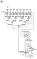
図2は、半導体装置の構成例を示すブロック図である。
図3Aは、メモリセルアレイの構成例を示すブロック図である。図3B、図3Cは、メモリセルの構成例を示す回路図である。
図4は、回路147の構成例を示す回路図である。
図5は、メモリセルの動作例を説明するタイミングチャートである。
図6は、階層型ニューラルネットワークの構成例を示す模式図である。
図7は、ビット線プロセッサの構成例を示す回路図である。
図8は、半導体装置の構成例を示す断面図である。
図9A乃至図9Cは、トランジスタの構造例を示す断面図である。
図10Aは、トランジスタの構造例を示す上面図である。図10B、図10Cは、トランジスタの構造例を示す断面図である。
図11Aは、トランジスタの構造例を示す上面図である。図11B、図11Cは、トランジスタの構造例を示す断面図である。
図12Aは、トランジスタの構造例を示す上面図である。図12B、図12Cは、トランジスタの構造例を示す断面図である。
図13Aは、トランジスタの構造例を示す上面図である。図13B、図13Cは、トランジスタの構造例を示す断面図である。
図14Aは、トランジスタの構造例を示す上面図である。図14B、図14Cは、トランジスタの構造例を示す断面図である。
図15Aは、トランジスタの構造例を示す上面図である。図15B、図15Cは、トランジスタの構造例を示す断面図である。
図16A、図16Bは、トランジスタの構造例を示す断面図である。
図17は、半導体装置の構成例を示す断面図である。
図18A、図18Bは、トランジスタの構造例を示す断面図である。
図19Aは、IGZOの結晶構造の分類を説明する図である。図19Bは、CAAC-IGZO膜のXRDスペクトルを説明する図である。図19Cは、CAAC-IGZO膜の極微電子線回折パターンを説明する図である。
本実施の形態では、本発明の一形態に係わる半導体装置の構成例および動作例について説明する。本発明の一形態に係わる半導体装置は、半導体特性を利用した記憶装置としての機能を有する。半導体特性を利用した記憶装置は、メモリとも呼ばれている。また、本発明の一形態に係わる半導体装置は、演算装置が有する演算機能の一部を有し、読み出したデータを用いて積和演算を行うことができる。
図1は、本発明の一形態に係わる半導体装置100の構成例を示す斜視概略図である。
図2は、半導体装置100の構成例を示すブロック図である。
図3Aは、メモリセルアレイ120の構成例を示すブロック図である。メモリセルアレイ120は、一列にm(mは2以上の整数)個、一行にn(nは2以上の整数)個、合計m×n個のメモリセル121を有する。メモリセル121は行列状に配置されている。
ビット線ドライバ回路142には、列ごとに、図4に示す回路147が設けられている。図4は、回路147の構成例を示す回路図である。なお、本実施の形態では、メモリセルアレイ120は、一行に128個のメモリセル121を有するものとする(n=128)。
図5は、メモリセル121の動作例を説明するタイミングチャートである。図5では、メモリセル121の書き込み動作および読み出し動作における、ワード線wwl、ワード線rwl、ビット線wbl、およびビット線rblの電位関係について説明する。
次に、パターン認識などに用いられる階層型ニューラルネットワークを例に挙げ、階層型ニューラルネットワークと積和演算の関係について説明する。図6は、階層型ニューラルネットワークの構成例を示す模式図である。
U[q]=Σp{W[q,p]×A[p]} (a5)
演算回路150は、4個のビット線プロセッサ151を有し、式a5の積和演算を行う機能を有する。図7は、ビット線プロセッサ151の構成例を示す回路図である。
本発明の一形態に係わる半導体装置は、例えば、8ビットの重み係数を同じ行のメモリセル121に保持し、重み係数をビット線ドライバ回路142から同時にビット線プロセッサ151に供給することができる。ビット線プロセッサ151は、積和演算を並列に行う機能を有し、半導体装置100は積和演算を行った結果を、別の半導体装置(演算装置等)に出力することができる。
本実施の形態では、上記実施の形態で説明した半導体装置100を構成する、トランジスタの構成例について説明する。本実施の形態では、単結晶シリコン基板に形成されたSiトランジスタを有する層の上方に、OSトランジスタを有する層が積層して設けられた構造を有する。
図8に示す半導体装置は、トランジスタ300、トランジスタ500、および容量素子600を有する。図9Aはトランジスタ500のチャネル長方向の断面図であり、図9Bはトランジスタ500のチャネル幅方向の断面図であり、図9Cはトランジスタ300のチャネル幅方向の断面図である。
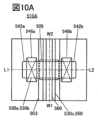
なお、本実施の形態に示す半導体装置のトランジスタ500は、上記の構造に限られるものではない。以下、トランジスタ500に用いることができる構造例について説明する。
図10A、図10Bおよび図10Cを用いてトランジスタ510Aの構造例を説明する。図10Aはトランジスタ510Aの上面図である。図10Bは、図10Aに一点鎖線L1-L2で示す部位の断面図である。図10Cは、図10Aに一点鎖線W1-W2で示す部位の断面図である。なお、図10Aの上面図では、図の明瞭化のために一部の要素を省いて図示している。
図11A、図11Bおよび図11Cを用いてトランジスタ510Bの構造例を説明する。図11Aはトランジスタ510Bの上面図である。図11Bは、図11Aに一点鎖線L1-L2で示す部位の断面図である。図11Cは、図11Aに一点鎖線W1-W2で示す部位の断面図である。なお、図11Aの上面図では、図の明瞭化のために一部の要素を省いて図示している。
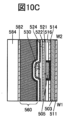
図12A、図12Bおよび図12Cを用いてトランジスタ510Cの構造例を説明する。図12Aはトランジスタ510Cの上面図である。図12Bは、図12Aに一点鎖線L1-L2で示す部位の断面図である。図12Cは、図12Aに一点鎖線W1-W2で示す部位の断面図である。なお、図12Aの上面図では、図の明瞭化のために一部の要素を省いて図示している。
図13A、図13Bおよび図13Cを用いてトランジスタ510Dの構造例を説明する。図13Aはトランジスタ510Dの上面図である。図13Bは、図13Aに一点鎖線L1-L2で示す部位の断面図である。図13Cは、図13Aに一点鎖線W1-W2で示す部位の断面図である。なお、図13Aの上面図では、図の明瞭化のために一部の要素を省いて図示している。
図14A、図14Bおよび図14Cを用いてトランジスタ510Eの構造例を説明する。図14Aはトランジスタ510Eの上面図である。図14Bは、図14Aに一点鎖線L1-L2で示す部位の断面図である。図14Cは、図14Aに一点鎖線W1-W2で示す部位の断面図である。なお、図14Aの上面図では、図の明瞭化のために一部の要素を省いて図示している。
図15A、図15Bおよび図15Cを用いてトランジスタ510Fの構造例を説明する。図15Aはトランジスタ510Fの上面図である。図15Bは、図15Aに一点鎖線L1-L2で示す部位の断面図である。図15Cは、図15Aに一点鎖線W1-W2で示す部位の断面図である。なお、図15Aの上面図では、図の明瞭化のために一部の要素を省いて図示している。
図16A、図16Bを用いてトランジスタ510Gの構造例を説明する。トランジスタ510Gはトランジスタ500の変形例である。よって、説明の繰り返しを防ぐため、主に上記トランジスタと異なる点について説明する。なお、図16A、図16Bに示す構成は、トランジスタ300等、本発明の一形態の半導体装置が有する他のトランジスタにも適用することができる。
本実施の形態では、金属酸化物の一種である酸化物半導体について説明する。
まず、酸化物半導体における、結晶構造の分類について、図19Aを用いて説明を行う。図19Aは、酸化物半導体、代表的にはIGZO(Inと、Gaと、Znと、を含む金属酸化物)の結晶構造の分類を説明する図である。
なお、酸化物半導体は、結晶構造に着目した場合、図19Aとは異なる分類となる場合がある。例えば、酸化物半導体は、単結晶酸化物半導体と、それ以外の非単結晶酸化物半導体と、に分けられる。非単結晶酸化物半導体としては、例えば、上述のCAAC-OS、及びnc-OSがある。また、非単結晶酸化物半導体には、多結晶酸化物半導体、擬似非晶質酸化物半導体(a-like OS:amorphous-like oxide semiconductor)、非晶質酸化物半導体、などが含まれる。
CAAC-OSは、複数の結晶領域を有し、当該複数の結晶領域はc軸が特定の方向に配向している酸化物半導体である。なお、特定の方向とは、CAAC-OS膜の厚さ方向、CAAC-OS膜の被形成面の法線方向、またはCAAC-OS膜の表面の法線方向である。また、結晶領域とは、原子配列に周期性を有する領域である。なお、原子配列を格子配列とみなすと、結晶領域とは、格子配列の揃った領域でもある。さらに、CAAC-OSは、a-b面方向において複数の結晶領域が連結する領域を有し、当該領域は歪みを有する場合がある。なお、歪みとは、複数の結晶領域が連結する領域において、格子配列の揃った領域と、別の格子配列の揃った領域と、の間で格子配列の向きが変化している箇所を指す。つまり、CAAC-OSは、c軸配向し、a-b面方向には明らかな配向をしていない酸化物半導体である。
nc-OSは、微小な領域(例えば、1nm以上10nm以下の領域、特に1nm以上3nm以下の領域)において原子配列に周期性を有する。別言すると、nc-OSは、微小な結晶を有する。なお、当該微小な結晶の大きさは、例えば、1nm以上10nm以下、特に1nm以上3nm以下であることから、当該微小な結晶をナノ結晶ともいう。また、nc-OSは、異なるナノ結晶間で結晶方位に規則性が見られない。そのため、膜全体で配向性が見られない。したがって、nc-OSは、分析方法によっては、a-like OSや非晶質酸化物半導体と区別が付かない場合がある。例えば、nc-OS膜に対し、XRD装置を用いて構造解析を行うと、θ/2θスキャンを用いたOut-of-plane XRD測定では、結晶性を示すピークが検出されない。また、nc-OS膜に対し、ナノ結晶よりも大きいプローブ径(例えば50nm以上)の電子線を用いる電子線回折(制限視野電子線回折ともいう)を行うと、ハローパターンのような回折パターンが観測される。一方、nc-OS膜に対し、ナノ結晶の大きさと近いかナノ結晶より小さいプローブ径(例えば1nm以上30nm以下)の電子線を用いる電子線回折(ナノビーム電子線回折ともいう)を行うと、ダイレクトスポットを中心とするリング状の領域内に複数のスポットが観測される電子線回折パターンが取得される場合がある。
a-like OSは、nc-OSと非晶質酸化物半導体との間の構造を有する酸化物半導体である。a-like OSは、鬆又は低密度領域を有する。即ち、a-like OSは、nc-OS及びCAAC-OSと比べて、結晶性が低い。また、a-like OSは、nc-OS及びCAAC-OSと比べて、膜中の水素濃度が高い。
次に、上述のCAC-OSの詳細について、説明を行う。なお、CAC-OSは材料構成に関する。
CAC-OSとは、例えば、金属酸化物を構成する元素が、0.5nm以上10nm以下、好ましくは、1nm以上3nm以下、またはその近傍のサイズで偏在した材料の一構成である。なお、以下では、金属酸化物において、一つまたは複数の金属元素が偏在し、該金属元素を有する領域が、0.5nm以上10nm以下、好ましくは、1nm以上3nm以下、またはその近傍のサイズで混合した状態をモザイク状、またはパッチ状ともいう。
続いて、上記酸化物半導体をトランジスタに用いる場合について説明する。
ここで、酸化物半導体中における各不純物の影響について説明する。
Claims (3)
- メモリセルアレイと、マルチプレクサ回路と、演算回路と、を有する半導体装置であって、
前記メモリセルアレイは、行列状に配置されたm×n個(m、nは2以上の整数)のメモリセルと、n本のビット線と、を有し、
前記マルチプレクサ回路は、n本の前記ビット線の中からs本(sは2以上n以下の整数)の前記ビット線を選択する機能と、s本の前記ビット線を介して前記メモリセルアレイから出力されたsビットの重み係数のデータを、前記演算回路に供給する機能と、を有し、
前記演算回路は、t個(tは1以上s未満の整数)の積和演算器を有し、
前記演算回路は、t個の前記積和演算器のそれぞれに、sビットの前記重み係数のデータからuビット(uは2以上の整数、t×uはs以下の整数)ずつ前記重み係数のデータを入力する機能を有し、
t個の前記積和演算器のそれぞれには、前記半導体装置の外部から入力されたuビットの第2のデータが入力され、
t個の前記積和演算器のそれぞれにおいて、uビットの前記重み係数のデータと、uビットの前記第2のデータとを用いた演算処理が行われる、
半導体装置。 - 請求項1において、
前記メモリセルは、トランジスタを有し、
前記トランジスタは、チャネル形成領域に金属酸化物を有する、
半導体装置。 - 請求項2において、
前記金属酸化物は、インジウム及び亜鉛の少なくとも一方を含む、
半導体装置。
Applications Claiming Priority (3)
| Application Number | Priority Date | Filing Date | Title |
|---|---|---|---|
| JP2019172147 | 2019-09-20 | ||
| JP2019172147 | 2019-09-20 | ||
| PCT/IB2020/058318 WO2021053453A1 (ja) | 2019-09-20 | 2020-09-08 | 半導体装置 |
Publications (3)
| Publication Number | Publication Date |
|---|---|
| JPWO2021053453A1 JPWO2021053453A1 (ja) | 2021-03-25 |
| JPWO2021053453A5 JPWO2021053453A5 (ja) | 2023-08-30 |
| JP7577671B2 true JP7577671B2 (ja) | 2024-11-05 |
Family
ID=74883969
Family Applications (1)
| Application Number | Title | Priority Date | Filing Date |
|---|---|---|---|
| JP2021546060A Active JP7577671B2 (ja) | 2019-09-20 | 2020-09-08 | 半導体装置 |
Country Status (4)
| Country | Link |
|---|---|
| US (1) | US12002535B2 (ja) |
| JP (1) | JP7577671B2 (ja) |
| DE (1) | DE112020004469T5 (ja) |
| WO (1) | WO2021053453A1 (ja) |
Families Citing this family (8)
| Publication number | Priority date | Publication date | Assignee | Title |
|---|---|---|---|---|
| US12069846B2 (en) * | 2019-01-29 | 2024-08-20 | Semiconductor Energy Laboratory Co., Ltd. | Memory device |
| US11908947B2 (en) | 2019-08-08 | 2024-02-20 | Semiconductor Energy Laboratory Co., Ltd. | Semiconductor device |
| WO2021130591A1 (ja) | 2019-12-27 | 2021-07-01 | 株式会社半導体エネルギー研究所 | 半導体装置 |
| JP7571127B2 (ja) | 2020-04-17 | 2024-10-22 | 株式会社半導体エネルギー研究所 | 半導体装置、及び電子機器 |
| CN114792688A (zh) * | 2021-01-26 | 2022-07-26 | 上峰科技股份有限公司 | 电子系统、与宽带隙半导体器件集成的可编程电阻存储器及其操作方法 |
| US11974422B2 (en) * | 2021-11-04 | 2024-04-30 | Taiwan Semiconductor Manufacturing Company, Ltd. | Semiconductor device |
| WO2025046433A1 (ja) * | 2023-08-31 | 2025-03-06 | 株式会社半導体エネルギー研究所 | 半導体装置 |
| WO2025153929A1 (ja) * | 2024-01-17 | 2025-07-24 | 株式会社半導体エネルギー研究所 | 半導体装置 |
Citations (1)
| Publication number | Priority date | Publication date | Assignee | Title |
|---|---|---|---|---|
| JP2019057053A (ja) | 2017-09-20 | 2019-04-11 | 東芝メモリ株式会社 | 半導体記憶装置 |
Family Cites Families (37)
| Publication number | Priority date | Publication date | Assignee | Title |
|---|---|---|---|---|
| JP3260357B2 (ja) | 1990-01-24 | 2002-02-25 | 株式会社日立製作所 | 情報処理装置 |
| TW330265B (en) | 1994-11-22 | 1998-04-21 | Hitachi Ltd | Semiconductor apparatus |
| JP3601883B2 (ja) | 1994-11-22 | 2004-12-15 | 株式会社ルネサステクノロジ | 半導体装置 |
| TWI555128B (zh) | 2010-08-06 | 2016-10-21 | 半導體能源研究所股份有限公司 | 半導體裝置及半導體裝置的驅動方法 |
| WO2012029638A1 (en) | 2010-09-03 | 2012-03-08 | Semiconductor Energy Laboratory Co., Ltd. | Semiconductor device |
| JP6001900B2 (ja) | 2011-04-21 | 2016-10-05 | 株式会社半導体エネルギー研究所 | 信号処理回路 |
| TWI536502B (zh) | 2011-05-13 | 2016-06-01 | 半導體能源研究所股份有限公司 | 記憶體電路及電子裝置 |
| US8837203B2 (en) | 2011-05-19 | 2014-09-16 | Semiconductor Energy Laboratory Co., Ltd. | Semiconductor device |
| JP6013682B2 (ja) | 2011-05-20 | 2016-10-25 | 株式会社半導体エネルギー研究所 | 半導体装置の駆動方法 |
| JP2013130802A (ja) | 2011-12-22 | 2013-07-04 | Semiconductor Energy Lab Co Ltd | 半導体装置、画像表示装置、記憶装置、及び電子機器 |
| KR102296696B1 (ko) | 2012-01-23 | 2021-09-02 | 가부시키가이샤 한도오따이 에네루기 켄큐쇼 | 반도체 장치 |
| US9372694B2 (en) | 2012-03-29 | 2016-06-21 | Semiconductor Energy Laboratory Co., Ltd. | Reducing data backup and recovery periods in processors |
| KR102044725B1 (ko) | 2012-03-29 | 2019-11-14 | 가부시키가이샤 한도오따이 에네루기 켄큐쇼 | 전원 제어 장치 |
| KR102107591B1 (ko) | 2012-07-18 | 2020-05-07 | 가부시키가이샤 한도오따이 에네루기 켄큐쇼 | 기억 소자 및 프로그래머블 로직 디바이스 |
| JP2014112213A (ja) | 2012-10-30 | 2014-06-19 | Semiconductor Energy Lab Co Ltd | 表示装置の駆動方法 |
| JP2014142986A (ja) | 2012-12-26 | 2014-08-07 | Semiconductor Energy Lab Co Ltd | 半導体装置 |
| US9786350B2 (en) | 2013-03-18 | 2017-10-10 | Semiconductor Energy Laboratory Co., Ltd. | Memory device |
| US9172369B2 (en) | 2013-05-17 | 2015-10-27 | Semiconductor Energy Laboratory Co., Ltd. | Programmable logic device and semiconductor device |
| US8994430B2 (en) | 2013-05-17 | 2015-03-31 | Semiconductor Energy Laboratory Co., Ltd. | Semiconductor device |
| US9406348B2 (en) | 2013-12-26 | 2016-08-02 | Semiconductor Energy Laboratory Co., Ltd. | Memory cell including transistor and capacitor |
| JP6442321B2 (ja) | 2014-03-07 | 2018-12-19 | 株式会社半導体エネルギー研究所 | 半導体装置及びその駆動方法、並びに電子機器 |
| JP6580863B2 (ja) | 2014-05-22 | 2019-09-25 | 株式会社半導体エネルギー研究所 | 半導体装置、健康管理システム |
| JP6754579B2 (ja) | 2015-02-09 | 2020-09-16 | 株式会社半導体エネルギー研究所 | 半導体装置、記憶装置、電子機器 |
| WO2016135591A1 (en) * | 2015-02-26 | 2016-09-01 | Semiconductor Energy Laboratory Co., Ltd. | Memory system and information processing system |
| JP6995481B2 (ja) | 2016-01-29 | 2022-02-04 | 株式会社半導体エネルギー研究所 | ソースドライバ |
| US10685614B2 (en) | 2016-03-17 | 2020-06-16 | Semiconductor Energy Laboratory Co., Ltd. | Display device, display module, and electronic device |
| US10242728B2 (en) * | 2016-10-27 | 2019-03-26 | Samsung Electronics Co., Ltd. | DPU architecture |
| US11314484B2 (en) | 2017-05-19 | 2022-04-26 | Semiconductor Energy Laboratory Co., Ltd. | Semiconductor device comprising operation circuits and switch circuits |
| DE112018003617T5 (de) | 2017-07-14 | 2020-06-04 | Semiconductor Energy Laboratory Co., Ltd. | Abbildungsvorrichtung und elektronisches Gerät |
| JP7004453B2 (ja) | 2017-08-11 | 2022-01-21 | 株式会社半導体エネルギー研究所 | グラフィックスプロセッシングユニット |
| JP7265479B2 (ja) | 2017-08-25 | 2023-04-26 | 株式会社半導体エネルギー研究所 | 半導体装置、および半導体装置の作製方法 |
| JP2019046199A (ja) | 2017-09-01 | 2019-03-22 | 株式会社半導体エネルギー研究所 | プロセッサ、および電子機器 |
| JP2019047006A (ja) | 2017-09-05 | 2019-03-22 | 株式会社半導体エネルギー研究所 | 半導体装置、電子機器 |
| JP7179740B2 (ja) | 2017-09-06 | 2022-11-29 | 株式会社半導体エネルギー研究所 | 電子機器 |
| JP2019056955A (ja) * | 2017-09-19 | 2019-04-11 | 東芝メモリ株式会社 | メモリシステム |
| US10607135B2 (en) | 2017-10-19 | 2020-03-31 | General Electric Company | Training an auto-encoder on a single class |
| US11322199B1 (en) * | 2020-10-09 | 2022-05-03 | Qualcomm Incorporated | Compute-in-memory (CIM) cell circuits employing capacitive storage circuits for reduced area and CIM bit cell array circuits |
-
2020
- 2020-09-08 JP JP2021546060A patent/JP7577671B2/ja active Active
- 2020-09-08 WO PCT/IB2020/058318 patent/WO2021053453A1/ja not_active Ceased
- 2020-09-08 US US17/640,452 patent/US12002535B2/en active Active
- 2020-09-08 DE DE112020004469.6T patent/DE112020004469T5/de active Pending
Patent Citations (1)
| Publication number | Priority date | Publication date | Assignee | Title |
|---|---|---|---|---|
| JP2019057053A (ja) | 2017-09-20 | 2019-04-11 | 東芝メモリ株式会社 | 半導体記憶装置 |
Also Published As
| Publication number | Publication date |
|---|---|
| US20220343954A1 (en) | 2022-10-27 |
| US12002535B2 (en) | 2024-06-04 |
| WO2021053453A1 (ja) | 2021-03-25 |
| JPWO2021053453A1 (ja) | 2021-03-25 |
| DE112020004469T5 (de) | 2022-08-04 |
Similar Documents
| Publication | Publication Date | Title |
|---|---|---|
| JP7577671B2 (ja) | 半導体装置 | |
| JP7208891B2 (ja) | 半導体装置の作製方法 | |
| JP7711271B2 (ja) | 記憶装置 | |
| JP7167038B2 (ja) | 半導体装置 | |
| CN110506328A (zh) | 半导体装置及半导体装置的制造方法 | |
| WO2019048984A1 (ja) | 半導体装置、および半導体装置の作製方法 | |
| JP7246376B2 (ja) | 記憶装置、および電子機器 | |
| CN110313070A (zh) | 半导体装置以及其制造方法 | |
| CN110709998A (zh) | 半导体装置以及其制造方法 | |
| JP7618404B2 (ja) | 記憶装置 | |
| JP7560469B2 (ja) | 半導体装置 | |
| JP2018181890A (ja) | 半導体装置 | |
| US12014175B2 (en) | Data processing system and operation method of data processing system | |
| CN110678989A (zh) | 半导体装置及半导体装置的制造方法 | |
| JP2025120272A (ja) | 半導体装置 | |
| JP2018201011A (ja) | 半導体装置、および半導体装置の作製方法 | |
| WO2018215878A1 (ja) | 半導体装置、および半導体装置の作製方法 | |
| JP7577661B2 (ja) | 情報処理システム、及びその動作方法 | |
| JP7467430B2 (ja) | 記憶装置 | |
| JP7769768B2 (ja) | 半導体装置 | |
| JP2018152399A (ja) | 半導体装置、および半導体装置の作製方法 |
Legal Events
| Date | Code | Title | Description |
|---|---|---|---|
| A521 | Request for written amendment filed |
Free format text: JAPANESE INTERMEDIATE CODE: A523 Effective date: 20230822 |
|
| A621 | Written request for application examination |
Free format text: JAPANESE INTERMEDIATE CODE: A621 Effective date: 20230822 |
|
| A131 | Notification of reasons for refusal |
Free format text: JAPANESE INTERMEDIATE CODE: A131 Effective date: 20240723 |
|
| A521 | Request for written amendment filed |
Free format text: JAPANESE INTERMEDIATE CODE: A523 Effective date: 20240918 |
|
| TRDD | Decision of grant or rejection written | ||
| A01 | Written decision to grant a patent or to grant a registration (utility model) |
Free format text: JAPANESE INTERMEDIATE CODE: A01 Effective date: 20241001 |
|
| A61 | First payment of annual fees (during grant procedure) |
Free format text: JAPANESE INTERMEDIATE CODE: A61 Effective date: 20241023 |
|
| R150 | Certificate of patent or registration of utility model |
Ref document number: 7577671 Country of ref document: JP Free format text: JAPANESE INTERMEDIATE CODE: R150 |