JP7489558B2 - Liquid crystal display device - Google Patents
Liquid crystal display device Download PDFInfo
- Publication number
- JP7489558B2 JP7489558B2 JP2024015853A JP2024015853A JP7489558B2 JP 7489558 B2 JP7489558 B2 JP 7489558B2 JP 2024015853 A JP2024015853 A JP 2024015853A JP 2024015853 A JP2024015853 A JP 2024015853A JP 7489558 B2 JP7489558 B2 JP 7489558B2
- Authority
- JP
- Japan
- Prior art keywords
- film
- wiring
- substrate
- region
- liquid crystal
- Prior art date
- Legal status (The legal status is an assumption and is not a legal conclusion. Google has not performed a legal analysis and makes no representation as to the accuracy of the status listed.)
- Active
Links
- 239000004973 liquid crystal related substance Substances 0.000 title claims description 88
- 239000004065 semiconductor Substances 0.000 claims description 191
- 230000015572 biosynthetic process Effects 0.000 claims description 46
- 239000010408 film Substances 0.000 description 447
- 239000010410 layer Substances 0.000 description 181
- 239000000758 substrate Substances 0.000 description 161
- 238000000034 method Methods 0.000 description 80
- 238000005530 etching Methods 0.000 description 77
- 239000010409 thin film Substances 0.000 description 66
- 239000007789 gas Substances 0.000 description 63
- 230000008569 process Effects 0.000 description 51
- 239000012535 impurity Substances 0.000 description 49
- 229910052739 hydrogen Inorganic materials 0.000 description 34
- 239000001257 hydrogen Substances 0.000 description 33
- 238000004519 manufacturing process Methods 0.000 description 32
- BLRPTPMANUNPDV-UHFFFAOYSA-N Silane Chemical compound [SiH4] BLRPTPMANUNPDV-UHFFFAOYSA-N 0.000 description 30
- UFHFLCQGNIYNRP-UHFFFAOYSA-N Hydrogen Chemical compound [H][H] UFHFLCQGNIYNRP-UHFFFAOYSA-N 0.000 description 28
- IJGRMHOSHXDMSA-UHFFFAOYSA-N Atomic nitrogen Chemical compound N#N IJGRMHOSHXDMSA-UHFFFAOYSA-N 0.000 description 20
- 230000006870 function Effects 0.000 description 20
- 239000011521 glass Substances 0.000 description 20
- 229910000077 silane Inorganic materials 0.000 description 18
- 229910052581 Si3N4 Inorganic materials 0.000 description 16
- QVGXLLKOCUKJST-UHFFFAOYSA-N atomic oxygen Chemical compound [O] QVGXLLKOCUKJST-UHFFFAOYSA-N 0.000 description 16
- 229910021424 microcrystalline silicon Inorganic materials 0.000 description 16
- 239000001301 oxygen Substances 0.000 description 16
- 229910052760 oxygen Inorganic materials 0.000 description 16
- HQVNEWCFYHHQES-UHFFFAOYSA-N silicon nitride Chemical compound N12[Si]34N5[Si]62N3[Si]51N64 HQVNEWCFYHHQES-UHFFFAOYSA-N 0.000 description 16
- 238000001312 dry etching Methods 0.000 description 15
- 229910052751 metal Inorganic materials 0.000 description 15
- 229910052782 aluminium Inorganic materials 0.000 description 14
- XAGFODPZIPBFFR-UHFFFAOYSA-N aluminium Chemical compound [Al] XAGFODPZIPBFFR-UHFFFAOYSA-N 0.000 description 14
- XUIMIQQOPSSXEZ-UHFFFAOYSA-N Silicon Chemical compound [Si] XUIMIQQOPSSXEZ-UHFFFAOYSA-N 0.000 description 13
- RTAQQCXQSZGOHL-UHFFFAOYSA-N Titanium Chemical compound [Ti] RTAQQCXQSZGOHL-UHFFFAOYSA-N 0.000 description 13
- 239000002184 metal Substances 0.000 description 13
- 229910052710 silicon Inorganic materials 0.000 description 13
- 239000010703 silicon Substances 0.000 description 13
- 229910052719 titanium Inorganic materials 0.000 description 13
- 239000010936 titanium Substances 0.000 description 13
- 229920001940 conductive polymer Polymers 0.000 description 12
- AMGQUBHHOARCQH-UHFFFAOYSA-N indium;oxotin Chemical compound [In].[Sn]=O AMGQUBHHOARCQH-UHFFFAOYSA-N 0.000 description 12
- 229910052990 silicon hydride Inorganic materials 0.000 description 12
- XYFCBTPGUUZFHI-UHFFFAOYSA-N Phosphine Chemical compound P XYFCBTPGUUZFHI-UHFFFAOYSA-N 0.000 description 11
- 238000010438 heat treatment Methods 0.000 description 11
- 239000000463 material Substances 0.000 description 11
- 238000011161 development Methods 0.000 description 10
- 239000000203 mixture Substances 0.000 description 10
- 229910052757 nitrogen Inorganic materials 0.000 description 10
- ZOKXTWBITQBERF-UHFFFAOYSA-N Molybdenum Chemical compound [Mo] ZOKXTWBITQBERF-UHFFFAOYSA-N 0.000 description 9
- 239000003990 capacitor Substances 0.000 description 9
- 238000009826 distribution Methods 0.000 description 9
- 229910052750 molybdenum Inorganic materials 0.000 description 9
- 239000011733 molybdenum Substances 0.000 description 9
- 238000005268 plasma chemical vapour deposition Methods 0.000 description 9
- 125000006850 spacer group Chemical group 0.000 description 9
- 238000004544 sputter deposition Methods 0.000 description 9
- 238000003860 storage Methods 0.000 description 9
- 239000002585 base Substances 0.000 description 8
- 238000000151 deposition Methods 0.000 description 8
- 239000011229 interlayer Substances 0.000 description 8
- 229920002120 photoresistant polymer Polymers 0.000 description 8
- 239000000460 chlorine Substances 0.000 description 7
- 239000013078 crystal Substances 0.000 description 7
- 230000008021 deposition Effects 0.000 description 7
- XKRFYHLGVUSROY-UHFFFAOYSA-N Argon Chemical compound [Ar] XKRFYHLGVUSROY-UHFFFAOYSA-N 0.000 description 6
- OAICVXFJPJFONN-UHFFFAOYSA-N Phosphorus Chemical compound [P] OAICVXFJPJFONN-UHFFFAOYSA-N 0.000 description 6
- 238000004380 ashing Methods 0.000 description 6
- 239000011651 chromium Substances 0.000 description 6
- 238000004140 cleaning Methods 0.000 description 6
- 230000005684 electric field Effects 0.000 description 6
- 238000005516 engineering process Methods 0.000 description 6
- 229910052698 phosphorus Inorganic materials 0.000 description 6
- 239000011574 phosphorus Substances 0.000 description 6
- 238000000206 photolithography Methods 0.000 description 6
- 238000009832 plasma treatment Methods 0.000 description 6
- ZAMOUSCENKQFHK-UHFFFAOYSA-N Chlorine atom Chemical compound [Cl] ZAMOUSCENKQFHK-UHFFFAOYSA-N 0.000 description 5
- GDTBXPJZTBHREO-UHFFFAOYSA-N bromine Substances BrBr GDTBXPJZTBHREO-UHFFFAOYSA-N 0.000 description 5
- 229910052801 chlorine Inorganic materials 0.000 description 5
- 239000011248 coating agent Substances 0.000 description 5
- 238000000576 coating method Methods 0.000 description 5
- 238000010586 diagram Methods 0.000 description 5
- 238000002844 melting Methods 0.000 description 5
- 230000008018 melting Effects 0.000 description 5
- 229910000073 phosphorus hydride Inorganic materials 0.000 description 5
- 239000002356 single layer Substances 0.000 description 5
- WFKWXMTUELFFGS-UHFFFAOYSA-N tungsten Chemical compound [W] WFKWXMTUELFFGS-UHFFFAOYSA-N 0.000 description 5
- 229910052721 tungsten Inorganic materials 0.000 description 5
- 239000010937 tungsten Substances 0.000 description 5
- ZCYVEMRRCGMTRW-UHFFFAOYSA-N 7553-56-2 Chemical compound [I] ZCYVEMRRCGMTRW-UHFFFAOYSA-N 0.000 description 4
- 229910000838 Al alloy Inorganic materials 0.000 description 4
- WKBOTKDWSSQWDR-UHFFFAOYSA-N Bromine atom Chemical compound [Br] WKBOTKDWSSQWDR-UHFFFAOYSA-N 0.000 description 4
- PXGOKWXKJXAPGV-UHFFFAOYSA-N Fluorine Chemical compound FF PXGOKWXKJXAPGV-UHFFFAOYSA-N 0.000 description 4
- -1 MoSiO Inorganic materials 0.000 description 4
- VYPSYNLAJGMNEJ-UHFFFAOYSA-N Silicium dioxide Chemical compound O=[Si]=O VYPSYNLAJGMNEJ-UHFFFAOYSA-N 0.000 description 4
- GWEVSGVZZGPLCZ-UHFFFAOYSA-N Titan oxide Chemical compound O=[Ti]=O GWEVSGVZZGPLCZ-UHFFFAOYSA-N 0.000 description 4
- 229910021417 amorphous silicon Inorganic materials 0.000 description 4
- 229910052794 bromium Inorganic materials 0.000 description 4
- 230000008859 change Effects 0.000 description 4
- 230000007423 decrease Effects 0.000 description 4
- 238000013461 design Methods 0.000 description 4
- 238000007865 diluting Methods 0.000 description 4
- 230000000694 effects Effects 0.000 description 4
- 238000002474 experimental method Methods 0.000 description 4
- 239000011737 fluorine Substances 0.000 description 4
- 229910052731 fluorine Inorganic materials 0.000 description 4
- 239000001307 helium Substances 0.000 description 4
- 229910052734 helium Inorganic materials 0.000 description 4
- SWQJXJOGLNCZEY-UHFFFAOYSA-N helium atom Chemical compound [He] SWQJXJOGLNCZEY-UHFFFAOYSA-N 0.000 description 4
- 229910003437 indium oxide Inorganic materials 0.000 description 4
- PJXISJQVUVHSOJ-UHFFFAOYSA-N indium(iii) oxide Chemical compound [O-2].[O-2].[O-2].[In+3].[In+3] PJXISJQVUVHSOJ-UHFFFAOYSA-N 0.000 description 4
- 239000011630 iodine Substances 0.000 description 4
- 229910052740 iodine Inorganic materials 0.000 description 4
- 239000011159 matrix material Substances 0.000 description 4
- QGLKJKCYBOYXKC-UHFFFAOYSA-N nonaoxidotritungsten Chemical compound O=[W]1(=O)O[W](=O)(=O)O[W](=O)(=O)O1 QGLKJKCYBOYXKC-UHFFFAOYSA-N 0.000 description 4
- 230000003647 oxidation Effects 0.000 description 4
- 238000007254 oxidation reaction Methods 0.000 description 4
- 239000000565 sealant Substances 0.000 description 4
- 229910052814 silicon oxide Inorganic materials 0.000 description 4
- 239000000126 substance Substances 0.000 description 4
- 229910052715 tantalum Inorganic materials 0.000 description 4
- GUVRBAGPIYLISA-UHFFFAOYSA-N tantalum atom Chemical compound [Ta] GUVRBAGPIYLISA-UHFFFAOYSA-N 0.000 description 4
- OGIDPMRJRNCKJF-UHFFFAOYSA-N titanium oxide Inorganic materials [Ti]=O OGIDPMRJRNCKJF-UHFFFAOYSA-N 0.000 description 4
- 229910001930 tungsten oxide Inorganic materials 0.000 description 4
- 238000001039 wet etching Methods 0.000 description 4
- YVTHLONGBIQYBO-UHFFFAOYSA-N zinc indium(3+) oxygen(2-) Chemical compound [O--].[Zn++].[In+3] YVTHLONGBIQYBO-UHFFFAOYSA-N 0.000 description 4
- KZBUYRJDOAKODT-UHFFFAOYSA-N Chlorine Chemical compound ClCl KZBUYRJDOAKODT-UHFFFAOYSA-N 0.000 description 3
- VYZAMTAEIAYCRO-UHFFFAOYSA-N Chromium Chemical compound [Cr] VYZAMTAEIAYCRO-UHFFFAOYSA-N 0.000 description 3
- RYGMFSIKBFXOCR-UHFFFAOYSA-N Copper Chemical compound [Cu] RYGMFSIKBFXOCR-UHFFFAOYSA-N 0.000 description 3
- 229910052786 argon Inorganic materials 0.000 description 3
- 229910052804 chromium Inorganic materials 0.000 description 3
- 239000004020 conductor Substances 0.000 description 3
- 229910052802 copper Inorganic materials 0.000 description 3
- 239000010949 copper Substances 0.000 description 3
- 238000005520 cutting process Methods 0.000 description 3
- 150000002431 hydrogen Chemical class 0.000 description 3
- 229920002521 macromolecule Polymers 0.000 description 3
- 150000004767 nitrides Chemical class 0.000 description 3
- 230000003071 parasitic effect Effects 0.000 description 3
- 238000001020 plasma etching Methods 0.000 description 3
- 229920003023 plastic Polymers 0.000 description 3
- 239000004033 plastic Substances 0.000 description 3
- 229920002620 polyvinyl fluoride Polymers 0.000 description 3
- 238000001771 vacuum deposition Methods 0.000 description 3
- ZOXJGFHDIHLPTG-UHFFFAOYSA-N Boron Chemical compound [B] ZOXJGFHDIHLPTG-UHFFFAOYSA-N 0.000 description 2
- OKTJSMMVPCPJKN-UHFFFAOYSA-N Carbon Chemical compound [C] OKTJSMMVPCPJKN-UHFFFAOYSA-N 0.000 description 2
- 229910052779 Neodymium Inorganic materials 0.000 description 2
- 230000001154 acute effect Effects 0.000 description 2
- 239000003513 alkali Substances 0.000 description 2
- 239000000956 alloy Substances 0.000 description 2
- 125000004429 atom Chemical group 0.000 description 2
- 230000004888 barrier function Effects 0.000 description 2
- 229910052796 boron Inorganic materials 0.000 description 2
- 229910052799 carbon Inorganic materials 0.000 description 2
- 238000006243 chemical reaction Methods 0.000 description 2
- 238000005229 chemical vapour deposition Methods 0.000 description 2
- 238000004891 communication Methods 0.000 description 2
- 150000001875 compounds Chemical class 0.000 description 2
- 238000001816 cooling Methods 0.000 description 2
- 229920001577 copolymer Polymers 0.000 description 2
- 238000009792 diffusion process Methods 0.000 description 2
- 239000011152 fibreglass Substances 0.000 description 2
- 230000006872 improvement Effects 0.000 description 2
- 229910052743 krypton Inorganic materials 0.000 description 2
- DNNSSWSSYDEUBZ-UHFFFAOYSA-N krypton atom Chemical compound [Kr] DNNSSWSSYDEUBZ-UHFFFAOYSA-N 0.000 description 2
- 230000007246 mechanism Effects 0.000 description 2
- 239000007769 metal material Substances 0.000 description 2
- 229910044991 metal oxide Inorganic materials 0.000 description 2
- 150000004706 metal oxides Chemical class 0.000 description 2
- VNWKTOKETHGBQD-UHFFFAOYSA-N methane Chemical class C VNWKTOKETHGBQD-UHFFFAOYSA-N 0.000 description 2
- QEFYFXOXNSNQGX-UHFFFAOYSA-N neodymium atom Chemical compound [Nd] QEFYFXOXNSNQGX-UHFFFAOYSA-N 0.000 description 2
- 229920000767 polyaniline Polymers 0.000 description 2
- 229920006267 polyester film Polymers 0.000 description 2
- 229920000128 polypyrrole Polymers 0.000 description 2
- 229920000123 polythiophene Polymers 0.000 description 2
- 230000009467 reduction Effects 0.000 description 2
- 229910052706 scandium Inorganic materials 0.000 description 2
- SIXSYDAISGFNSX-UHFFFAOYSA-N scandium atom Chemical compound [Sc] SIXSYDAISGFNSX-UHFFFAOYSA-N 0.000 description 2
- 239000003566 sealing material Substances 0.000 description 2
- SFZCNBIFKDRMGX-UHFFFAOYSA-N sulfur hexafluoride Chemical compound FS(F)(F)(F)(F)F SFZCNBIFKDRMGX-UHFFFAOYSA-N 0.000 description 2
- 238000002834 transmittance Methods 0.000 description 2
- XLYOFNOQVPJJNP-UHFFFAOYSA-N water Chemical compound O XLYOFNOQVPJJNP-UHFFFAOYSA-N 0.000 description 2
- MWRNXFLKMVJUFL-UHFFFAOYSA-N $l^{2}-germane Chemical class [GeH2] MWRNXFLKMVJUFL-UHFFFAOYSA-N 0.000 description 1
- 239000004925 Acrylic resin Substances 0.000 description 1
- 229920000178 Acrylic resin Polymers 0.000 description 1
- 229910020323 ClF3 Inorganic materials 0.000 description 1
- 229910019974 CrSi Inorganic materials 0.000 description 1
- 101100441092 Danio rerio crlf3 gene Proteins 0.000 description 1
- OTMSDBZUPAUEDD-UHFFFAOYSA-N Ethane Chemical compound CC OTMSDBZUPAUEDD-UHFFFAOYSA-N 0.000 description 1
- GYHNNYVSQQEPJS-UHFFFAOYSA-N Gallium Chemical compound [Ga] GYHNNYVSQQEPJS-UHFFFAOYSA-N 0.000 description 1
- 229910006160 GeF4 Inorganic materials 0.000 description 1
- 229910016006 MoSi Inorganic materials 0.000 description 1
- 238000006124 Pilkington process Methods 0.000 description 1
- 229910007264 Si2H6 Inorganic materials 0.000 description 1
- 229910003902 SiCl 4 Inorganic materials 0.000 description 1
- 229910003910 SiCl4 Inorganic materials 0.000 description 1
- 229910004014 SiF4 Inorganic materials 0.000 description 1
- 229910003818 SiH2Cl2 Inorganic materials 0.000 description 1
- 229910003822 SiHCl3 Inorganic materials 0.000 description 1
- HCHKCACWOHOZIP-UHFFFAOYSA-N Zinc Chemical compound [Zn] HCHKCACWOHOZIP-UHFFFAOYSA-N 0.000 description 1
- XLOMVQKBTHCTTD-UHFFFAOYSA-N Zinc monoxide Chemical compound [Zn]=O XLOMVQKBTHCTTD-UHFFFAOYSA-N 0.000 description 1
- 229910052783 alkali metal Inorganic materials 0.000 description 1
- 150000001340 alkali metals Chemical class 0.000 description 1
- 229910045601 alloy Inorganic materials 0.000 description 1
- 239000005407 aluminoborosilicate glass Substances 0.000 description 1
- 239000005354 aluminosilicate glass Substances 0.000 description 1
- 229910052788 barium Inorganic materials 0.000 description 1
- DSAJWYNOEDNPEQ-UHFFFAOYSA-N barium atom Chemical compound [Ba] DSAJWYNOEDNPEQ-UHFFFAOYSA-N 0.000 description 1
- 239000011324 bead Substances 0.000 description 1
- 230000005540 biological transmission Effects 0.000 description 1
- 239000005388 borosilicate glass Substances 0.000 description 1
- 239000006227 byproduct Substances 0.000 description 1
- 239000000969 carrier Substances 0.000 description 1
- 239000000919 ceramic Substances 0.000 description 1
- 238000011109 contamination Methods 0.000 description 1
- 238000007796 conventional method Methods 0.000 description 1
- 230000003247 decreasing effect Effects 0.000 description 1
- 230000007547 defect Effects 0.000 description 1
- 230000006866 deterioration Effects 0.000 description 1
- 239000003989 dielectric material Substances 0.000 description 1
- PZPGRFITIJYNEJ-UHFFFAOYSA-N disilane Chemical compound [SiH3][SiH3] PZPGRFITIJYNEJ-UHFFFAOYSA-N 0.000 description 1
- 230000005669 field effect Effects 0.000 description 1
- 239000011888 foil Substances 0.000 description 1
- 229910052733 gallium Inorganic materials 0.000 description 1
- QUZPNFFHZPRKJD-UHFFFAOYSA-N germane Chemical compound [GeH4] QUZPNFFHZPRKJD-UHFFFAOYSA-N 0.000 description 1
- 229910052732 germanium Inorganic materials 0.000 description 1
- GNPVGFCGXDBREM-UHFFFAOYSA-N germanium atom Chemical compound [Ge] GNPVGFCGXDBREM-UHFFFAOYSA-N 0.000 description 1
- GGJOARIBACGTDV-UHFFFAOYSA-N germanium difluoride Chemical class F[Ge]F GGJOARIBACGTDV-UHFFFAOYSA-N 0.000 description 1
- 229910052986 germanium hydride Inorganic materials 0.000 description 1
- PCHJSUWPFVWCPO-UHFFFAOYSA-N gold Chemical compound [Au] PCHJSUWPFVWCPO-UHFFFAOYSA-N 0.000 description 1
- 229910052737 gold Inorganic materials 0.000 description 1
- 239000010931 gold Substances 0.000 description 1
- 229910052736 halogen Inorganic materials 0.000 description 1
- 150000002367 halogens Chemical class 0.000 description 1
- 125000004435 hydrogen atom Chemical group [H]* 0.000 description 1
- 229910052738 indium Inorganic materials 0.000 description 1
- APFVFJFRJDLVQX-UHFFFAOYSA-N indium atom Chemical compound [In] APFVFJFRJDLVQX-UHFFFAOYSA-N 0.000 description 1
- 238000007641 inkjet printing Methods 0.000 description 1
- 239000012212 insulator Substances 0.000 description 1
- 238000005342 ion exchange Methods 0.000 description 1
- 150000002500 ions Chemical class 0.000 description 1
- 239000000155 melt Substances 0.000 description 1
- 238000002156 mixing Methods 0.000 description 1
- 229910021421 monocrystalline silicon Inorganic materials 0.000 description 1
- 229910052754 neon Inorganic materials 0.000 description 1
- GKAOGPIIYCISHV-UHFFFAOYSA-N neon atom Chemical compound [Ne] GKAOGPIIYCISHV-UHFFFAOYSA-N 0.000 description 1
- 230000006911 nucleation Effects 0.000 description 1
- 238000010899 nucleation Methods 0.000 description 1
- 239000005416 organic matter Substances 0.000 description 1
- 238000007500 overflow downdraw method Methods 0.000 description 1
- 230000002093 peripheral effect Effects 0.000 description 1
- 229910021420 polycrystalline silicon Inorganic materials 0.000 description 1
- 239000000843 powder Substances 0.000 description 1
- 230000002265 prevention Effects 0.000 description 1
- 230000001737 promoting effect Effects 0.000 description 1
- 239000011347 resin Substances 0.000 description 1
- 229920005989 resin Polymers 0.000 description 1
- FDNAPBUWERUEDA-UHFFFAOYSA-N silicon tetrachloride Chemical compound Cl[Si](Cl)(Cl)Cl FDNAPBUWERUEDA-UHFFFAOYSA-N 0.000 description 1
- ABTOQLMXBSRXSM-UHFFFAOYSA-N silicon tetrafluoride Chemical compound F[Si](F)(F)F ABTOQLMXBSRXSM-UHFFFAOYSA-N 0.000 description 1
- 239000010935 stainless steel Substances 0.000 description 1
- 229910001220 stainless steel Inorganic materials 0.000 description 1
- 239000002344 surface layer Substances 0.000 description 1
- MZLGASXMSKOWSE-UHFFFAOYSA-N tantalum nitride Chemical compound [Ta]#N MZLGASXMSKOWSE-UHFFFAOYSA-N 0.000 description 1
- PPMWWXLUCOODDK-UHFFFAOYSA-N tetrafluorogermane Chemical compound F[Ge](F)(F)F PPMWWXLUCOODDK-UHFFFAOYSA-N 0.000 description 1
- TXEYQDLBPFQVAA-UHFFFAOYSA-N tetrafluoromethane Chemical compound FC(F)(F)F TXEYQDLBPFQVAA-UHFFFAOYSA-N 0.000 description 1
- 238000012546 transfer Methods 0.000 description 1
- JOHWNGGYGAVMGU-UHFFFAOYSA-N trifluorochlorine Chemical compound FCl(F)F JOHWNGGYGAVMGU-UHFFFAOYSA-N 0.000 description 1
- 229910052724 xenon Inorganic materials 0.000 description 1
- FHNFHKCVQCLJFQ-UHFFFAOYSA-N xenon atom Chemical compound [Xe] FHNFHKCVQCLJFQ-UHFFFAOYSA-N 0.000 description 1
- 229910052725 zinc Inorganic materials 0.000 description 1
- 239000011701 zinc Substances 0.000 description 1
Images


Classifications
-
- G—PHYSICS
- G02—OPTICS
- G02F—OPTICAL DEVICES OR ARRANGEMENTS FOR THE CONTROL OF LIGHT BY MODIFICATION OF THE OPTICAL PROPERTIES OF THE MEDIA OF THE ELEMENTS INVOLVED THEREIN; NON-LINEAR OPTICS; FREQUENCY-CHANGING OF LIGHT; OPTICAL LOGIC ELEMENTS; OPTICAL ANALOGUE/DIGITAL CONVERTERS
- G02F1/00—Devices or arrangements for the control of the intensity, colour, phase, polarisation or direction of light arriving from an independent light source, e.g. switching, gating or modulating; Non-linear optics
- G02F1/01—Devices or arrangements for the control of the intensity, colour, phase, polarisation or direction of light arriving from an independent light source, e.g. switching, gating or modulating; Non-linear optics for the control of the intensity, phase, polarisation or colour
- G02F1/13—Devices or arrangements for the control of the intensity, colour, phase, polarisation or direction of light arriving from an independent light source, e.g. switching, gating or modulating; Non-linear optics for the control of the intensity, phase, polarisation or colour based on liquid crystals, e.g. single liquid crystal display cells
- G02F1/133—Constructional arrangements; Operation of liquid crystal cells; Circuit arrangements
- G02F1/1333—Constructional arrangements; Manufacturing methods
- G02F1/1345—Conductors connecting electrodes to cell terminals
- G02F1/13458—Terminal pads
-
- H—ELECTRICITY
- H01—ELECTRIC ELEMENTS
- H01L—SEMICONDUCTOR DEVICES NOT COVERED BY CLASS H10
- H01L29/00—Semiconductor devices specially adapted for rectifying, amplifying, oscillating or switching and having potential barriers; Capacitors or resistors having potential barriers, e.g. a PN-junction depletion layer or carrier concentration layer; Details of semiconductor bodies or of electrodes thereof ; Multistep manufacturing processes therefor
- H01L29/40—Electrodes ; Multistep manufacturing processes therefor
- H01L29/41—Electrodes ; Multistep manufacturing processes therefor characterised by their shape, relative sizes or dispositions
- H01L29/423—Electrodes ; Multistep manufacturing processes therefor characterised by their shape, relative sizes or dispositions not carrying the current to be rectified, amplified or switched
- H01L29/42312—Gate electrodes for field effect devices
- H01L29/42316—Gate electrodes for field effect devices for field-effect transistors
- H01L29/4232—Gate electrodes for field effect devices for field-effect transistors with insulated gate
- H01L29/42384—Gate electrodes for field effect devices for field-effect transistors with insulated gate for thin film field effect transistors, e.g. characterised by the thickness or the shape of the insulator or the dimensions, the shape or the lay-out of the conductor
-
- G—PHYSICS
- G02—OPTICS
- G02F—OPTICAL DEVICES OR ARRANGEMENTS FOR THE CONTROL OF LIGHT BY MODIFICATION OF THE OPTICAL PROPERTIES OF THE MEDIA OF THE ELEMENTS INVOLVED THEREIN; NON-LINEAR OPTICS; FREQUENCY-CHANGING OF LIGHT; OPTICAL LOGIC ELEMENTS; OPTICAL ANALOGUE/DIGITAL CONVERTERS
- G02F1/00—Devices or arrangements for the control of the intensity, colour, phase, polarisation or direction of light arriving from an independent light source, e.g. switching, gating or modulating; Non-linear optics
- G02F1/01—Devices or arrangements for the control of the intensity, colour, phase, polarisation or direction of light arriving from an independent light source, e.g. switching, gating or modulating; Non-linear optics for the control of the intensity, phase, polarisation or colour
- G02F1/13—Devices or arrangements for the control of the intensity, colour, phase, polarisation or direction of light arriving from an independent light source, e.g. switching, gating or modulating; Non-linear optics for the control of the intensity, phase, polarisation or colour based on liquid crystals, e.g. single liquid crystal display cells
- G02F1/133—Constructional arrangements; Operation of liquid crystal cells; Circuit arrangements
- G02F1/1333—Constructional arrangements; Manufacturing methods
- G02F1/1345—Conductors connecting electrodes to cell terminals
- G02F1/13452—Conductors connecting driver circuitry and terminals of panels
-
- H—ELECTRICITY
- H01—ELECTRIC ELEMENTS
- H01L—SEMICONDUCTOR DEVICES NOT COVERED BY CLASS H10
- H01L27/00—Devices consisting of a plurality of semiconductor or other solid-state components formed in or on a common substrate
- H01L27/02—Devices consisting of a plurality of semiconductor or other solid-state components formed in or on a common substrate including semiconductor components specially adapted for rectifying, oscillating, amplifying or switching and having potential barriers; including integrated passive circuit elements having potential barriers
- H01L27/12—Devices consisting of a plurality of semiconductor or other solid-state components formed in or on a common substrate including semiconductor components specially adapted for rectifying, oscillating, amplifying or switching and having potential barriers; including integrated passive circuit elements having potential barriers the substrate being other than a semiconductor body, e.g. an insulating body
- H01L27/1214—Devices consisting of a plurality of semiconductor or other solid-state components formed in or on a common substrate including semiconductor components specially adapted for rectifying, oscillating, amplifying or switching and having potential barriers; including integrated passive circuit elements having potential barriers the substrate being other than a semiconductor body, e.g. an insulating body comprising a plurality of TFTs formed on a non-semiconducting substrate, e.g. driving circuits for AMLCDs
- H01L27/124—Devices consisting of a plurality of semiconductor or other solid-state components formed in or on a common substrate including semiconductor components specially adapted for rectifying, oscillating, amplifying or switching and having potential barriers; including integrated passive circuit elements having potential barriers the substrate being other than a semiconductor body, e.g. an insulating body comprising a plurality of TFTs formed on a non-semiconducting substrate, e.g. driving circuits for AMLCDs with a particular composition, shape or layout of the wiring layers specially adapted to the circuit arrangement, e.g. scanning lines in LCD pixel circuits
- H01L27/1244—Devices consisting of a plurality of semiconductor or other solid-state components formed in or on a common substrate including semiconductor components specially adapted for rectifying, oscillating, amplifying or switching and having potential barriers; including integrated passive circuit elements having potential barriers the substrate being other than a semiconductor body, e.g. an insulating body comprising a plurality of TFTs formed on a non-semiconducting substrate, e.g. driving circuits for AMLCDs with a particular composition, shape or layout of the wiring layers specially adapted to the circuit arrangement, e.g. scanning lines in LCD pixel circuits for preventing breakage, peeling or short circuiting
-
- H—ELECTRICITY
- H01—ELECTRIC ELEMENTS
- H01L—SEMICONDUCTOR DEVICES NOT COVERED BY CLASS H10
- H01L27/00—Devices consisting of a plurality of semiconductor or other solid-state components formed in or on a common substrate
- H01L27/02—Devices consisting of a plurality of semiconductor or other solid-state components formed in or on a common substrate including semiconductor components specially adapted for rectifying, oscillating, amplifying or switching and having potential barriers; including integrated passive circuit elements having potential barriers
- H01L27/12—Devices consisting of a plurality of semiconductor or other solid-state components formed in or on a common substrate including semiconductor components specially adapted for rectifying, oscillating, amplifying or switching and having potential barriers; including integrated passive circuit elements having potential barriers the substrate being other than a semiconductor body, e.g. an insulating body
- H01L27/1214—Devices consisting of a plurality of semiconductor or other solid-state components formed in or on a common substrate including semiconductor components specially adapted for rectifying, oscillating, amplifying or switching and having potential barriers; including integrated passive circuit elements having potential barriers the substrate being other than a semiconductor body, e.g. an insulating body comprising a plurality of TFTs formed on a non-semiconducting substrate, e.g. driving circuits for AMLCDs
- H01L27/1259—Multistep manufacturing methods
- H01L27/1288—Multistep manufacturing methods employing particular masking sequences or specially adapted masks, e.g. half-tone mask
-
- H—ELECTRICITY
- H01—ELECTRIC ELEMENTS
- H01L—SEMICONDUCTOR DEVICES NOT COVERED BY CLASS H10
- H01L29/00—Semiconductor devices specially adapted for rectifying, amplifying, oscillating or switching and having potential barriers; Capacitors or resistors having potential barriers, e.g. a PN-junction depletion layer or carrier concentration layer; Details of semiconductor bodies or of electrodes thereof ; Multistep manufacturing processes therefor
- H01L29/02—Semiconductor bodies ; Multistep manufacturing processes therefor
- H01L29/04—Semiconductor bodies ; Multistep manufacturing processes therefor characterised by their crystalline structure, e.g. polycrystalline, cubic or particular orientation of crystalline planes
-
- H—ELECTRICITY
- H01—ELECTRIC ELEMENTS
- H01L—SEMICONDUCTOR DEVICES NOT COVERED BY CLASS H10
- H01L29/00—Semiconductor devices specially adapted for rectifying, amplifying, oscillating or switching and having potential barriers; Capacitors or resistors having potential barriers, e.g. a PN-junction depletion layer or carrier concentration layer; Details of semiconductor bodies or of electrodes thereof ; Multistep manufacturing processes therefor
- H01L29/40—Electrodes ; Multistep manufacturing processes therefor
- H01L29/43—Electrodes ; Multistep manufacturing processes therefor characterised by the materials of which they are formed
- H01L29/49—Metal-insulator-semiconductor electrodes, e.g. gates of MOSFET
- H01L29/4908—Metal-insulator-semiconductor electrodes, e.g. gates of MOSFET for thin film semiconductor, e.g. gate of TFT
-
- H—ELECTRICITY
- H01—ELECTRIC ELEMENTS
- H01L—SEMICONDUCTOR DEVICES NOT COVERED BY CLASS H10
- H01L29/00—Semiconductor devices specially adapted for rectifying, amplifying, oscillating or switching and having potential barriers; Capacitors or resistors having potential barriers, e.g. a PN-junction depletion layer or carrier concentration layer; Details of semiconductor bodies or of electrodes thereof ; Multistep manufacturing processes therefor
- H01L29/66—Types of semiconductor device ; Multistep manufacturing processes therefor
- H01L29/66007—Multistep manufacturing processes
- H01L29/66075—Multistep manufacturing processes of devices having semiconductor bodies comprising group 14 or group 13/15 materials
- H01L29/66227—Multistep manufacturing processes of devices having semiconductor bodies comprising group 14 or group 13/15 materials the devices being controllable only by the electric current supplied or the electric potential applied, to an electrode which does not carry the current to be rectified, amplified or switched, e.g. three-terminal devices
- H01L29/66409—Unipolar field-effect transistors
- H01L29/66477—Unipolar field-effect transistors with an insulated gate, i.e. MISFET
- H01L29/66742—Thin film unipolar transistors
- H01L29/6675—Amorphous silicon or polysilicon transistors
- H01L29/66765—Lateral single gate single channel transistors with inverted structure, i.e. the channel layer is formed after the gate
-
- H—ELECTRICITY
- H01—ELECTRIC ELEMENTS
- H01L—SEMICONDUCTOR DEVICES NOT COVERED BY CLASS H10
- H01L29/00—Semiconductor devices specially adapted for rectifying, amplifying, oscillating or switching and having potential barriers; Capacitors or resistors having potential barriers, e.g. a PN-junction depletion layer or carrier concentration layer; Details of semiconductor bodies or of electrodes thereof ; Multistep manufacturing processes therefor
- H01L29/66—Types of semiconductor device ; Multistep manufacturing processes therefor
- H01L29/68—Types of semiconductor device ; Multistep manufacturing processes therefor controllable by only the electric current supplied, or only the electric potential applied, to an electrode which does not carry the current to be rectified, amplified or switched
- H01L29/76—Unipolar devices, e.g. field effect transistors
- H01L29/772—Field effect transistors
- H01L29/78—Field effect transistors with field effect produced by an insulated gate
- H01L29/786—Thin film transistors, i.e. transistors with a channel being at least partly a thin film
- H01L29/78696—Thin film transistors, i.e. transistors with a channel being at least partly a thin film characterised by the structure of the channel, e.g. multichannel, transverse or longitudinal shape, length or width, doping structure, or the overlap or alignment between the channel and the gate, the source or the drain, or the contacting structure of the channel
-
- G—PHYSICS
- G02—OPTICS
- G02F—OPTICAL DEVICES OR ARRANGEMENTS FOR THE CONTROL OF LIGHT BY MODIFICATION OF THE OPTICAL PROPERTIES OF THE MEDIA OF THE ELEMENTS INVOLVED THEREIN; NON-LINEAR OPTICS; FREQUENCY-CHANGING OF LIGHT; OPTICAL LOGIC ELEMENTS; OPTICAL ANALOGUE/DIGITAL CONVERTERS
- G02F1/00—Devices or arrangements for the control of the intensity, colour, phase, polarisation or direction of light arriving from an independent light source, e.g. switching, gating or modulating; Non-linear optics
- G02F1/01—Devices or arrangements for the control of the intensity, colour, phase, polarisation or direction of light arriving from an independent light source, e.g. switching, gating or modulating; Non-linear optics for the control of the intensity, phase, polarisation or colour
- G02F1/13—Devices or arrangements for the control of the intensity, colour, phase, polarisation or direction of light arriving from an independent light source, e.g. switching, gating or modulating; Non-linear optics for the control of the intensity, phase, polarisation or colour based on liquid crystals, e.g. single liquid crystal display cells
- G02F1/133—Constructional arrangements; Operation of liquid crystal cells; Circuit arrangements
- G02F1/136—Liquid crystal cells structurally associated with a semi-conducting layer or substrate, e.g. cells forming part of an integrated circuit
- G02F1/1362—Active matrix addressed cells
- G02F1/136231—Active matrix addressed cells for reducing the number of lithographic steps
- G02F1/136236—Active matrix addressed cells for reducing the number of lithographic steps using a grey or half tone lithographic process
Landscapes
- Engineering & Computer Science (AREA)
- Power Engineering (AREA)
- Physics & Mathematics (AREA)
- Microelectronics & Electronic Packaging (AREA)
- General Physics & Mathematics (AREA)
- Condensed Matter Physics & Semiconductors (AREA)
- Computer Hardware Design (AREA)
- Ceramic Engineering (AREA)
- Nonlinear Science (AREA)
- Crystallography & Structural Chemistry (AREA)
- Chemical & Material Sciences (AREA)
- Manufacturing & Machinery (AREA)
- Mathematical Physics (AREA)
- Optics & Photonics (AREA)
- Liquid Crystal (AREA)
- Thin Film Transistor (AREA)
- Internal Circuitry In Semiconductor Integrated Circuit Devices (AREA)
- Electrodes Of Semiconductors (AREA)
- Devices For Indicating Variable Information By Combining Individual Elements (AREA)
- Drying Of Semiconductors (AREA)
- Exposure Of Semiconductors, Excluding Electron Or Ion Beam Exposure (AREA)
Description
本発明は薄膜トランジスタ(以下、TFTという)で構成された回路を有する半導体装
置およびその作製方法に関する。例えば、液晶表示パネルに代表される電気光学装置や有
機発光素子を有する発光表示装置を部品として搭載した電子機器に関する。
The present invention relates to a semiconductor device having a circuit formed of thin film transistors (hereinafter referred to as TFTs) and a manufacturing method thereof, and more particularly to electronic equipment incorporating, as a component, an electro-optical device such as a liquid crystal display panel or a light-emitting display device having an organic light-emitting element.
なお、本明細書中において半導体装置とは、半導体特性を利用することで機能しうる装
置全般を指し、電気光学装置、半導体回路および電子機器は全て半導体装置である。
In this specification, the term "semiconductor device" refers to any device that can function by utilizing semiconductor characteristics, and electro-optical devices, semiconductor circuits, and electronic devices are all classified as semiconductor devices.
近年、絶縁表面を有する基板上に形成された半導体薄膜(厚さ数~数百nm程度)を用
いて薄膜トランジスタ(TFT)を構成する技術が注目されている。薄膜トランジスタは
ICや電気光学装置のような電子デバイスに広く応用され、特に画像表示装置のスイッチ
ング素子として開発が急がれている。
In recent years, attention has been focused on a technology for constructing thin film transistors (TFTs) using a semiconductor thin film (with a thickness of about several to several hundred nm) formed on a substrate having an insulating surface. Thin film transistors are widely used in electronic devices such as ICs and electro-optical devices, and their development as switching elements in image display devices is being particularly accelerated.
特に、マトリクス状に配置された表示画素毎にTFTからなるスイッチング素子を設け
たアクティブマトリクス型の表示装置(液晶表示装置や発光表示装置)が盛んに開発され
ている。
In particular, active matrix display devices (liquid crystal display devices and light emitting display devices) in which a switching element made of a TFT is provided for each display pixel arranged in a matrix are being actively developed.
この画像表示装置のスイッチング素子は、高精細な画像表示を得るために、面積効率よく
配置することができる高精細なフォトリソグラフィ技術が要求される。
In order to obtain a high-definition image display, the switching elements of this image display device require high-definition photolithography technology that allows for area-efficient arrangement.
また、これまで、一枚のマザーガラス基板から複数のパネルを切り出して、大量生産を効
率良く行う生産技術が採用されてきた。マザーガラス基板のサイズは、1990年初頭に
おける第1世代の300×400mmから、2000年には第4世代となり680×88
0mm若しくは730×920mmへと大型化して、一枚の基板から多数の表示パネルが
取れるように生産技術が進歩してきた。今後、さらにマザーガラス基板のサイズは、大型
化するため、例えば第10世代の3mを超えるサイズの基板にも対応する必要がある。
In addition, production techniques have been adopted to efficiently mass-produce multiple panels by cutting them out from a single mother glass substrate. The size of the mother glass substrate has increased from 300 x 400 mm for the first generation in the early 1990s to 680 x 88 mm for the fourth generation in 2000.
As mother glass substrates have become larger, to 730 x 920 mm or 730 x 920 mm, production technology has advanced to the point where multiple display panels can be produced from a single substrate. In the future, mother glass substrates will continue to become larger, so it will be necessary to accommodate substrates that exceed 3 m in size, for example, for the 10th generation.
高精細な画像表示を得る表示装置を得るためには、マザーガラス基板上に成膜された金属
薄膜に対してフォトリソグラフィ技術により得られるレジストマスクを用いてエッチング
して配線を形成する。
In order to obtain a display device that can display high-definition images, wiring is formed by etching a metal thin film formed on a mother glass substrate using a resist mask obtained by photolithography.
エッチング方法には、様々な方法があるが、大きく分けてドライエッチング方法とウェッ
トエッチング方法とが挙げられる。ウェットエッチング方法は等方性エッチングのため、
レジストマスクで保護された配線層の側面がある程度削り取られてしまい、微細化には不
向きとされている。
There are various etching methods, but they can be roughly divided into dry etching and wet etching. Wet etching is an isotropic etching method, so
The sides of the wiring layer protected by the resist mask are removed to a certain extent, making this method unsuitable for miniaturization.
また、一般に知られているドライエッチング方法は、RIEドライエッチング方法であり
、異方性エッチングである。異方性エッチングであるため、微細化には等方性エッチング
であるウェットエッチング方法と比べて有利とされている。
A commonly known dry etching method is an RIE dry etching method, which is an anisotropic etching method, and is considered to be more advantageous for miniaturization than a wet etching method, which is an isotropic etching method.
また、ICPエッチング装置を用いて断面形状がテーパー形状を有するタングステン配線
が特許文献1に開示されている。
Furthermore,
また、回折格子パターン或いは半透膜からなる光強度低減機能を有する補助パターンを設
置したフォトマスク或いはレチクルをゲート電極形成用フォトリソグラフィ工程に適用し
たTFT作製工程が特許文献2に開示されている。
Furthermore, Patent Document 2 discloses a TFT manufacturing process in which a photomask or reticle having an auxiliary pattern having a light intensity reducing function made of a diffraction grating pattern or a semi-transparent film is applied to a photolithography process for forming a gate electrode.
また、レジストマスク幅およびエッチング条件を調節することで配線の断面形状を部分的
に異ならせる技術が特許文献3で開示されている。
Furthermore,
また、半透膜からなる光強度低減機能を有する補助パターンを設置したフォトマスクを用
いてソース電極またはドレイン電極を形成する技術が特許文献4に開示されている。
Furthermore,
1枚のマザーガラス基板上に配線を形成する場合、従来の方法では、同じ断面形状の配線
となってしまう。例えば、RIEドライエッチング方法を用いる場合、現像したレジスト
を加熱して溶かしてレジスト形状を変形させた後、エッチングを行うことでレジスト形状
を反映させて配線の側面をテーパー形状としている。この場合、レジストを加熱するプロ
セスが増加することとなる。また、溶かしてレジスト面積を拡大させるため、隣り合う配
線の間隔を狭くすることが困難である。また、多層配線を形成する場合、配線を形成しよ
うとする領域の下方に配線がある場合には、レジストを溶かす際に下方の配線も加熱され
るため、レジスト加熱温度が不均一となり場所によってレジストが溶けて広がる割合が変
化してしまい、所望の配線形状を得ることが困難である。
When wiring is formed on one mother glass substrate, the conventional method results in wiring with the same cross-sectional shape. For example, when using the RIE dry etching method, the developed resist is heated and melted to deform the resist shape, and then etching is performed to reflect the resist shape and make the side of the wiring have a tapered shape. In this case, the process of heating the resist is increased. In addition, since the resist area is expanded by melting, it is difficult to narrow the interval between adjacent wirings. In addition, when forming multi-layer wiring, if there is wiring below the region where wiring is to be formed, the lower wiring is also heated when melting the resist, so the resist heating temperature becomes non-uniform and the rate at which the resist melts and spreads varies depending on the location, making it difficult to obtain the desired wiring shape.
また、ICPエッチング装置を用いる場合、コイル状アンテナを用いるため、長方形であ
る1枚のマザーガラス基板全面に渡って一様な放電を得ることが困難である。
Furthermore, when an ICP etching device is used, it is difficult to obtain a uniform discharge over the entire surface of a single rectangular mother glass substrate because a coil antenna is used.
例えば、透過型の液晶表示装置の画素部において、ゲート配線をテーパ形状とすることで
薄い半導体層をその上に形成する一方、テーパー形状とすると配線幅が広がるため、開口
率の低下を招く恐れがある。また、テーパー形状とすると配線幅が広がるため、その配線
と絶縁膜を介して重なる他の配線が存在すると、不要な寄生容量が形成される。この寄生
容量を小さくするために、異なる層に配置する配線同士が重ならないように各層の配線の
レイアウトを行うと、開口率の低下を招くこととなってしまう。
For example, in the pixel portion of a transmissive liquid crystal display device, a gate wiring is tapered and a thin semiconductor layer is formed on it, but the tapered shape increases the wiring width, which may lead to a decrease in aperture ratio. In addition, the tapered shape increases the wiring width, so if there is another wiring that overlaps the wiring through an insulating film, unnecessary parasitic capacitance is formed. In order to reduce this parasitic capacitance, if the wiring of each layer is laid out so that the wirings arranged in different layers do not overlap each other, this leads to a decrease in aperture ratio.
また、回折格子パターン或いは半透膜からなる光強度低減機能を有する補助パターンを設
置したフォトマスクを用いる場合、選択的に配線の断面形状を異ならせることができる。
この場合、配線の側面が2段の階段状の部分と、そうでない部分との2種類の断面形状の
配線となってしまう。
Furthermore, when a photomask having an auxiliary pattern having a diffraction grating pattern or a semi-transparent film and a light intensity reducing function is used, the cross-sectional shape of the wiring can be selectively made different.
In this case, the side surface of the wiring will have two types of cross-sectional shapes, a portion having a two-step shaped staircase and a portion not having such a shaped staircase.
半導体装置の作製方法において、工程を増やすことなく、1枚のマザーガラス基板上に所
望の部分にそれぞれ精密に配線の側面の角度を異ならせた配線を提供することを課題とす
る。
An object of the present invention is to provide wirings, the angles of the side surfaces of which are precisely different, in desired portions on one mother glass substrate, without increasing the number of steps in a manufacturing method of a semiconductor device.
露光光を透過可能な透光性基板と、透光性基板に形成されたクロム等からなる遮光部と、
所定の線幅で遮光材料からなるラインおよびスペースが繰り返し形成された光強度低減機
能を有する半透過部とを備えた露光マスクを用いる。ラインおよびスペースで形成された
半透過部を備えた露光マスクをグレートーン露光用マスクともいい、この露光マスクを用
いた露光をグレートーン露光ともいう。
a light-transmitting substrate capable of transmitting exposure light; and a light-shielding portion formed on the light-transmitting substrate and made of chromium or the like;
An exposure mask having a semi-transmitting portion having a light intensity reducing function in which lines and spaces made of a light-shielding material are repeatedly formed with a predetermined line width is used. An exposure mask having semi-transmitting portions formed of lines and spaces is also called a graytone exposure mask, and exposure using this exposure mask is also called graytone exposure.
グレートーン露光用マスクは、スリット、ドット等のパターンが少なくとも1つ以上、周
期的あるいは非周期的に配置された開口パターンを有している。なお、露光装置の解像限
界以下のラインおよびスペースから成るマスクの開口のスペースで構成される光強度低減
機能を有する補助パターンの光強度は、10~70%の範囲で調整可能となっている。
A graytone exposure mask has an aperture pattern that is periodically or non-periodically arranged with at least one pattern such as slits, dots, etc. The light intensity of the auxiliary pattern having a light intensity reduction function, which is composed of the spaces of the mask apertures that are composed of lines and spaces below the resolution limit of the exposure device, can be adjusted within the range of 10 to 70%.
また、露光光の光強度を低減する機能を有する半透過膜からなる半透過部を備えた露光マ
スクは、ハーフトーン露光用マスクともいい、この露光マスクを用いた露光をハーフトー
ン露光ともいう。半透過膜としては、MoSiNの他に、MoSi、MoSiO、MoS
iON、CrSiなどを用いることができる。
In addition, an exposure mask having a semi-transparent portion made of a semi-transparent film having a function of reducing the light intensity of exposure light is also called a half-tone exposure mask, and exposure using this exposure mask is also called half-tone exposure. As the semi-transparent film, in addition to MoSiN, MoSi, MoSiO, MoS
For example, iON, CrSi, etc. can be used.
なお、本明細書において、グレートーン露光用マスクや、ハーフトーン露光用マスクを総
称して、便宜上、多階調マスクと呼ぶ。
In this specification, a gray-tone exposure mask and a half-tone exposure mask are collectively referred to as a multi-tone mask for convenience.
多階調マスクを用いることで1つのフォトレジスト層を1枚のマザーガラス基板から遠ざ
かる方向に向かって断面積が連続的に減少するテーパ形状を有するフォトレジスト層を形
成する。本発明は、グレートーン露光用マスクまたはハーフトーン露光用マスクを用いる
ことで1つのフォトレジスト層を2つの異なる膜厚に現像し、フォトレジスト層の両端に
それぞれ1つの段差を形成するのではない。
By using a multi-tone mask, a photoresist layer having a tapered shape in which the cross-sectional area continuously decreases in the direction away from a single mother glass substrate is formed. The present invention does not use a gray-tone exposure mask or a half-tone exposure mask to develop a single photoresist layer to two different film thicknesses and form a step at each end of the photoresist layer.
本発明は、1本の配線を形成する際、1枚のフォトマスクを用い、第1の領域の部分には
グレートーン露光(またはハーフトーン露光)が行われ、同時に第2の領域の部分には通
常の露光が行われる。その後、現像を行い、金属膜を選択的にエッチングすることで、場
所によって側面形状(具体的には基板主平面に対する角度)が異なる1本の配線を得る。
この方法により、意図的に配線の側面形状を異ならせることができ、実施者にとって、所
望の配線を得ることができる。
In the present invention, when forming one wiring, one photomask is used, gray-tone exposure (or half-tone exposure) is performed on the first region, and at the same time, normal exposure is performed on the second region. Then, development is performed and the metal film is selectively etched to obtain one wiring whose side shape (specifically, the angle with respect to the main plane of the substrate) differs depending on the location.
This method allows the side shape of the wiring to be intentionally varied, allowing the practitioner to obtain the desired wiring.
結果的に第1の領域の配線における側面の幅(テーパー部分の幅とも呼ぶ)は、第2の領
域の配線における側面の幅よりも広くなる。また、第1の領域は、基板主平面に対する側
面の角度が第2の領域よりも小さくなる。
As a result, the width of the side surface of the wiring in the first region (also referred to as the width of the tapered portion) is wider than the width of the side surface of the wiring in the second region, and the angle of the side surface of the first region with respect to the main substrate plane is smaller than that of the second region.
1本の配線において、少なくとも第1の領域の部分と第2の領域の部分とは、基板主平面
に対する側面の角度の差が10°より大きくなるようにすることが好ましい。
In one wiring, it is preferable that the difference in angle of the side surface of at least the first region and the second region with respect to the main substrate plane is greater than 10°.
例えば、透過型の液晶表示装置において、半導体層と重なるゲート電極となる領域を第1
の領域として電気特性の優れた薄膜トランジスタを形成し、画素電極の間に延材するゲー
ト配線となる領域を第2の領域としてテーパー部の幅を狭くすることで開口率を向上させ
る。また、ゲート配線は配線抵抗を低減させ、且つ、開口率を向上させるために、テーパ
ー部の幅を狭くすることが好ましい。なお、トータルのゲート配線幅は、ゲート電極のト
ータルの電極幅よりも広くすることで、配線抵抗を低減できる。
For example, in a transmissive liquid crystal display device, a region that becomes a gate electrode and overlaps with a semiconductor layer is called a first
A thin film transistor having excellent electrical characteristics is formed as the first region, and a region that becomes a gate wiring extending between pixel electrodes is formed as the second region, and the width of the tapered portion is narrowed to improve the aperture ratio. In addition, it is preferable that the width of the tapered portion of the gate wiring is narrowed in order to reduce the wiring resistance and improve the aperture ratio. Note that the wiring resistance can be reduced by making the total gate wiring width wider than the total electrode width of the gate electrodes.
本明細書で開示する発明の構成は、基板上に半導体層と、半導体層と一部重なる配線とを
有し、配線は、配線側部の幅の広い領域と配線側部の幅の狭い領域とを有し、配線側部の
幅が広い領域は、半導体層と少なくとも一部重なり、且つ、配線側部の幅が狭い領域の配
線幅方向断面の側面角度と比べて配線幅方向断面の側面角度が10°以上小さいことを特
徴とする半導体装置である。
The configuration of the invention disclosed in this specification is a semiconductor device having a semiconductor layer on a substrate and wiring that partially overlaps the semiconductor layer, the wiring having a wide region on the side of the wiring and a narrow region on the side of the wiring, the wide region on the side of the wiring at least partially overlapping the semiconductor layer, and the side angle of the cross section in the wiring width direction is smaller by 10° or more than the side angle of the cross section in the wiring width direction of the narrow region on the side of the wiring.
具体的には、配線側部の幅の広い領域の配線幅方向断面の側面角度は、10°から50°
の範囲とし、配線側部の幅が狭い領域の配線幅方向断面の側面角度は、60°から90°
の範囲とする。なお、配線幅方向断面の側面角度が、90°であれば配線の断面形状は長
方形または正方形であり、90°未満であれば配線の断面形状は、上辺が底辺より短い台
形である。
Specifically, the side angle of the cross section in the width direction of the wiring in the wide region of the wiring side is 10° to 50°.
The side angle of the cross section in the wiring width direction in the narrow region of the wiring side is in the range of 60° to 90°.
If the side angle of the cross section in the wiring width direction is 90°, the cross section of the wiring is rectangular or square, and if it is less than 90°, the cross section of the wiring is a trapezoid with the top side shorter than the bottom side.
逆スタガ型の薄膜トランジスタにおいては、ゲート配線上に形成される半導体層は約50
nmと薄いため、ゲート配線側部の幅の広い領域の配線幅方向断面の側面角度は、10°
から50°の範囲として、ゲート配線の端部または側面と重なる半導体層の一部が薄膜化
しないようにすることが好ましい。
In the case of an inverted staggered thin film transistor, the semiconductor layer formed on the gate wiring is about 50
Since the thickness is as thin as 10 nm, the side angle of the cross section in the line width direction in the wide region on the side of the gate line is 10°.
It is preferable to set the angle within the range of 0.5 to 50° so that a part of the semiconductor layer overlapping the end or side of the gate wiring is not thinned.
本発明は、上記課題の少なくとも一つを解決する。 The present invention solves at least one of the above problems.
また、ゲート配線に限定されず、層間絶縁膜上にソース配線やドレイン配線や接続配線な
どの他の配線を形成する場合にも本発明を用いることができる。
Furthermore, the present invention is not limited to being used for gate wiring, but can also be used for forming other wiring such as source wiring, drain wiring, and connection wiring on an interlayer insulating film.
また、断面において配線の端部の両端に同じ角度の側面を有する配線を形成するだけでな
く、一方の側面と他方の側面の基板主平面に対する角度を異ならせることもできる。この
場合、配線の断面形状は、底辺に接する2つの内角が異なる台形と言える。
In addition to forming a wiring having side surfaces at the same angle on both ends of the wiring in cross section, it is also possible to make one side surface and the other side surface have different angles relative to the main plane of the substrate. In this case, the cross-sectional shape of the wiring can be said to be a trapezoid with two different interior angles that contact the base.
また、他の発明の構成は、基板上に第1の配線と、第1の配線を覆う絶縁膜と、絶縁膜を
介して第1の配線と電気的に接続する第2の配線とを有し、第2の配線の断面形状におけ
る2つの端部のうち、一方の側面と他方の側面との基板主平面に対する角度が異なる半導
体装置である。
Another aspect of the present invention is a semiconductor device having a first wiring on a substrate, an insulating film covering the first wiring, and a second wiring electrically connected to the first wiring via the insulating film, and one side and the other side of two ends of the cross-sectional shape of the second wiring have different angles with respect to the main substrate plane.
さらに、上記構成に加え、第2の配線と一部重なる透明導電膜を有し、透明導電膜は、第
2の配線の断面形状における2つの端部のうち、基板主平面に対する角度が小さい一方の
側面と接する。このような構成とすることによって第2の配線の一方の側面と重なる透明
導電膜との電気的な接続を確実に行い、透明導電膜の断線を低減する。
In addition to the above configuration, the transparent conductive film is provided so as to overlap a portion of the second wiring, and the transparent conductive film contacts one of the two ends of the second wiring in the cross-sectional shape that has a smaller angle with respect to the main plane of the substrate. By adopting such a configuration, electrical connection between the transparent conductive film and the one side of the second wiring is reliably established, thereby reducing disconnection of the transparent conductive film.
また、他の発明の構成は、グレートーン露光用マスクまたはハーフトーン露光用マスクを
用いることで1つのフォトレジスト層を3つ以上の異なる膜厚に現像し、フォトレジスト
層の両端にそれぞれ2つ以上の段差を形成する。このフォトレジスト層をマスクとして導
電層をエッチングすると、得られる配線の断面形状は、一方の側面に段差を2つ以上有す
る階段状となる。勿論、この断面形状を有する配線は、選択的に形成することができるた
め、同一絶縁膜表面上に第1の配線と、第1の配線と断面形状の異なる第2の配線とを有
し、第1の配線の断面形状は、長方形または台形であり、第2の配線の断面形状は、一方
の側面に段差を2つ以上有する階段状であり、第1の配線と第2の配線は、同じ材料であ
る半導体装置とすることができる。配線の断面形状をテーパー形状とする場合、テーパー
の端部の位置がエッチング時間によって左右され、特にテーパー角60°未満とするとト
ータルの配線幅にバラツキが生じる恐れや、側面が湾曲した曲面となって裾状となり、断
面積が減少して配線抵抗が増大する恐れがあるが、階段状とすることで、エッチング時間
が多少違っても一定の配線幅を得ることができる。即ち、第2の配線の断面形状を階段状
の配線層とすることでエッチング条件のマージンを十分にとることができる。さらに、第
2の配線の断面形状において2つの段差を有する端部とすることで、テーパー角50°未
満のテーパー形状を有する配線と同程度の段差被覆性を確保することができる。
In addition, another aspect of the present invention is to develop one photoresist layer to three or more different film thicknesses by using a gray-tone exposure mask or a half-tone exposure mask, and form two or more steps on each end of the photoresist layer. When the conductive layer is etched using this photoresist layer as a mask, the cross-sectional shape of the resulting wiring is a staircase shape having two or more steps on one side. Of course, since the wiring having this cross-sectional shape can be selectively formed, it is possible to provide a semiconductor device having a first wiring and a second wiring having a cross-sectional shape different from the first wiring on the same insulating film surface, the cross-sectional shape of the first wiring being rectangular or trapezoidal, the cross-sectional shape of the second wiring being a staircase shape having two or more steps on one side, and the first wiring and the second wiring being made of the same material. When the cross-sectional shape of the wiring is tapered, the position of the end of the taper depends on the etching time, and especially when the taper angle is less than 60°, there is a risk that the total wiring width will vary, or the side will be curved and have a skirt shape, which will reduce the cross-sectional area and increase the wiring resistance. However, by making it step-shaped, a constant wiring width can be obtained even if the etching time varies slightly. That is, by making the cross-sectional shape of the second wiring a step-shaped wiring layer, a sufficient margin of etching conditions can be obtained. Furthermore, by making the end of the second wiring have two steps in the cross-sectional shape, it is possible to ensure the same level of step coverage as a wiring having a tapered shape with a taper angle of less than 50°.
なお、一本の配線において、第1の領域の断面形状を長方形または台形とし、第2の領域
の断面形状を一方の側面に段差を2つ以上有する階段状とすることもできる。
In one wiring, the cross-sectional shape of the first region can be a rectangle or a trapezoid, and the cross-sectional shape of the second region can be a staircase shape having two or more steps on one side surface.
また、上記構造を実現するための作製方法に関する発明の構成は、基板上に導電層を形
成し、多階調マスクを用いて、1回の露光を行い、断面における側面と基板主平面とがな
す角が異なる第1のレジストマスクと第2のレジストマスクを現像し、第1のレジストマ
スクと第2のレジストマスクをマスクとして導電層をエッチングしてそれぞれ配線を形成
し、現像後の第1のレジストマスクの側断面の角度と、第2のレジストマスクの側断面の
角度との差は10°よりも大きい半導体装置の作製方法である。
The configuration of the invention relating to a manufacturing method for realizing the above structure is a method for manufacturing a semiconductor device, which includes forming a conductive layer on a substrate, performing a single exposure using a multi-tone mask, developing a first resist mask and a second resist mask having different angles between the side surface in a cross section and the main plane of the substrate, and etching the conductive layer using the first resist mask and the second resist mask as masks to form wirings, and the difference between the angle of the side cross section of the first resist mask after development and the angle of the side cross section of the second resist mask is greater than 10°.
また、他の作製方法に関する発明の構成は、基板上に導電層を形成し、多階調マスクを用
いて、1回の露光を行い、断面における側面と基板主平面とがなす角が異なる第1のレジ
ストマスクと第2のレジストマスクを現像し、第1のレジストマスクと第2のレジストマ
スクをマスクとして導電層をエッチングして1本の配線を形成し、現像後の第1のレジス
トマスクの側断面の角度と、第2のレジストマスクの側断面の角度との差は10°よりも
大きい半導体装置の作製方法である。
Another configuration of the invention relating to a manufacturing method is a method for manufacturing a semiconductor device, which includes forming a conductive layer on a substrate, performing a single exposure using a multi-tone mask, developing a first resist mask and a second resist mask having different angles between the side surface in a cross section and the main plane of the substrate, etching the conductive layer using the first resist mask and the second resist mask as masks to form one wiring, and the difference between the angle of the side cross section of the first resist mask after development and the angle of the side cross section of the second resist mask is greater than 10°.
上記各作製方法において、第1のレジストマスクの断面形状は、長方形または台形であり
、第2のレジストマスクの断面形状は、台形である。或いは、上記作製方法において、第
1のレジストマスクの断面形状は、長方形または台形であり、第2のレジストマスクの断
面形状は、一方の側面に段差を2つ以上有する階段状である。
In each of the above manufacturing methods, the cross-sectional shape of the first resist mask is a rectangle or a trapezoid, and the cross-sectional shape of the second resist mask is a trapezoid, or, in the above manufacturing methods, the cross-sectional shape of the first resist mask is a rectangle or a trapezoid, and the cross-sectional shape of the second resist mask is a stepped shape having two or more steps on one side surface.
上述したこれらの手段は単なる設計事項ではなく、多階調マスクを用いて実際に配線を形
成し、発明者らの深い検討の後、発明された事項である。
The above-mentioned means are not merely design matters, but are matters that have been invented after the inventors have actually formed wiring using a multi-tone mask and have made extensive considerations.
特許文献1に開示の技術は、ICPエッチング装置のエッチング条件によって、配線の側
面における角度が決定されるため、同一基板上に、同じエッチング工程で形成される配線
の側面形状は、全ての配線において一定とすることを意図している。従って、意図的に配
線の側面形状を場所によって異ならせる本発明とは大きく異なっている。
The technology disclosed in
また、特許文献2及び特許文献4に開示の技術は、レジストマスクの側部を階段状とし、
そのレジストマスクの形状を反映させて配線の側面も階段状としている。特許文献2及び
特許文献4に開示されている配線の段差は一つであり、両端のそれぞれ設けられている。
In addition, the techniques disclosed in
The side surface of the wiring is also formed in a stepped shape to reflect the shape of the resist mask. The wiring disclosed in
また、特許文献3に開示の技術は、配線の断面形状を部分的に異ならせる技術であるが、
同じエッチング工程で形成される配線の側面と基板主平面とがなす角度は同じである。
The technology disclosed in
The side surface of the wiring formed in the same etching process forms the same angle with the main surface of the substrate.
なお、本明細書において、上、下、側、水平、垂直等の方向を表す文言は、基板表面の上
にデバイスを配置した場合の基板面を基準とする方向を指す。
In this specification, terms expressing directions such as up, down, side, horizontal, vertical, etc. refer to directions based on the substrate surface when a device is disposed on the substrate surface.
また、本明細書において、ゲート電極とは、半導体層とゲート絶縁膜を介して重なり、薄
膜トランジスタのチャネルを形成する部分を指し、ゲート配線とは、それ以外の部分を指
す。なお、同じ導電材料からなる一つのパターンの一部がゲート電極であり、その他の部
分がゲート配線となる。
In this specification, the term "gate electrode" refers to a portion that overlaps with the semiconductor layer via a gate insulating film and forms a channel of a thin film transistor, and the term "gate wiring" refers to the other portion. Note that a part of one pattern made of the same conductive material is the gate electrode, and the other portion is the gate wiring.
また、本発明において、半導体層は、珪素を主成分とする半導体膜、或いは金属酸化物
を主成分とする半導体膜を用いることができる。珪素を主成分とする半導体膜としては、
非晶質半導体膜、結晶構造を含む半導体膜、非晶質構造を含む化合物半導体膜などを用い
ることができ、具体的にはアモルファスシリコン、微結晶シリコン、多結晶シリコン、単
結晶シリコンなどを用いることができる。また、金属酸化物を主成分とする半導体膜とし
ては、酸化亜鉛(ZnO)や亜鉛とガリウムとインジウムの酸化物(In-Ga-Zn-
O)等を用いることができる。
In the present invention, the semiconductor layer may be a semiconductor film containing silicon as a main component or a semiconductor film containing metal oxide as a main component.
Amorphous semiconductor films, semiconductor films including a crystalline structure, compound semiconductor films including an amorphous structure, and the like can be used. Specifically, amorphous silicon, microcrystalline silicon, polycrystalline silicon, single crystal silicon, and the like can be used. In addition, as a semiconductor film mainly composed of a metal oxide, zinc oxide (ZnO) and oxide of zinc, gallium, and indium (In-Ga-Zn-
O) and the like can be used.
また、TFT構造やトランジスタ構造に関係なく本発明を適用することが可能であり、
例えば、トップゲート型TFTや、ボトムゲート型(逆スタガ型)TFTや、順スタガ型
TFTを用いることが可能である。また、シングルゲート構造のトランジスタに限定され
ず、複数のチャネル形成領域を有するマルチゲート型トランジスタ、例えばダブルゲート
型トランジスタとしてもよい。
In addition, the present invention can be applied regardless of the TFT structure or transistor structure.
For example, a top-gate type TFT, a bottom-gate type (inverse staggered type) TFT, or a forward staggered type TFT can be used. In addition, the TFT is not limited to a single-gate type transistor, and may be a multi-gate type transistor having a plurality of channel formation regions, such as a double-gate type transistor.
1枚のマスクを用いて、工程を増やすことなく、1枚のマザーガラス基板上に所望の部分
にそれぞれ精密に配線の側面の角度を異ならせた配線を作製することができる。
By using one mask, and without increasing the number of processes, wirings having side surfaces with precisely different angles can be fabricated in desired locations on a single mother glass substrate.
本発明の実施形態について、以下に説明する。 An embodiment of the present invention is described below.
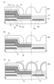
(実施の形態1)
本実施の形態は、薄膜トランジスタを有する画素部と、FPCなどを用いて外部装置と接
続するための接続配線を有する端子部とを同一基板上に形成する作製工程を図1に示す。
(Embodiment 1)
In this embodiment mode, a manufacturing process is shown in FIG. 1 in which a pixel portion having a thin film transistor and a terminal portion having a connection wiring for connecting to an external device using an FPC or the like are formed over the same substrate.
まず、絶縁表面を有する基板101を用意する。絶縁表面を有する基板101としては
、透光性を有する基板、例えばガラス基板、結晶化ガラス基板、もしくはプラスチック基
板を用いることができる。基板101がマザーガラスの場合、基板の大きさは、第1世代
(320mm×400mm)、第2世代(400mm×500mm)、第3世代(550
mm×650mm)、第4世代(680mm×880mm、または730mm×920m
m)、第5世代(1000mm×1200mmまたは1100mm×1250mm)、第
6世代1500mm×1800mm)、第7世代(1900mm×2200mm)、第8
世代(2160mm×2460mm)、第9世代(2400mm×2800mm、245
0mm×3050mm)、第10世代(2950mm×3400mm)等を用いることが
できる。
First, a
mm x 650 mm), 4th generation (680 mm x 880 mm, or 730 mm x 920 mm
m), 5th generation (1000mm x 1200mm or 1100mm x 1250mm), 6th generation 1500mm x 1800mm), 7th generation (1900mm x 2200mm), 8th generation
Generation (2160mm x 2460mm), 9th generation (2400mm x 2800mm, 245
10th generation (2950 mm x 3400 mm), 10th generation (2950 mm x 3050 mm), etc. can be used.
また、絶縁表面を有する基板101は、最表面となる層または膜が絶縁表面を有していれ
ば、絶縁体からなる下地膜や半導体層、または導電膜を既に形成していてもよい。
In addition, the
次に、絶縁表面を有する基板101上に、第1の導電層103を形成する。第1の導電
層103はタングステン、チタン、クロム、タンタル、またはモリブデンなどの高融点金
属、又は窒化タンタルなどの高融点金属を主成分とする合金もしくは化合物を200nm
~600nmの厚さで形成する。また、配線の低抵抗化を図るために、アルミニウム、金
、銅などの金属膜と上記高融点金属の積層としてもよい。
Next, a first
In order to reduce the resistance of the wiring, a metal film such as aluminum, gold, or copper may be laminated with the above-mentioned high melting point metal.
次いで、第1の導電層103上にレジスト膜403を全面に塗布した後、図1(A)に
示すマスク400を用いて露光を行う。ここでは、膜厚1.5μmのレジスト膜を塗布し
、露光は、解像度が1.5μmの露光機を用いる。露光に用いる光は、i線(波長365
nm)であり、露光エネルギーは、70~140mJ/cm2の範囲から選択する。また
、i線に限定されず、i線とg線(波長436nm)とh線(波長405nm)とを混合
させた光を露光に用いてもよい。
Next, a resist film 403 is applied to the entire surface of the first
nm), and the exposure energy is selected from the range of 70 to 140 mJ/ cm2 . In addition, the light is not limited to the i-line, and a mixture of the i-line, the g-line (wavelength 436 nm), and the h-line (wavelength 405 nm) may be used for exposure.
本実施の形態では、第1のフォトマスクとして露光マスクの一部に光強度低減機能を有
する補助パターン(グレートーン)を設置したものを用いて画素部の薄膜トランジスタの
ゲート電極のテーパ角を10°から50°の範囲とする。
In this embodiment, the first photomask is an exposure mask having an auxiliary pattern (gray tone) having a light intensity reducing function in a part thereof, and the taper angle of the gate electrode of the thin film transistor in the pixel portion is set in the range of 10° to 50°.
図1(A)において、露光マスク400は、Crなどの金属膜からなる遮光部401b
と、光強度低減機能を有する補助パターンとして、スリットが設けられた半透過部401
aとが設置されている。露光マスク400の断面図において、遮光部401bの幅をt2
と示し、半透過部401aの幅をt1とt3と示す。ここでは露光マスクの一部としてグ
レートーンを用いた例を示したが、半透膜を用いるハーフトーンを用いてもよい。
In FIG. 1A, the
and a semi-transmitting portion 401 having a slit as an auxiliary pattern having a light intensity reducing function.
In the cross-sectional view of the
and the widths of the
図1(A)に示す露光マスク400を用いてレジスト膜403の露光を行うと、レジス
ト膜403に非露光領域403a、403bと露光領域403cが形成される。露光時に
は、光が遮光部401bの回り込みや半透過部401aを通過することによって図1(A
)に示す露光領域403cが形成される。
When a resist film 403 is exposed using an
) is formed.
そして、現像を行うと、露光領域403cが除去されて、図1(B)に示すように、画
素部に第1のレジストマスク404aと、端子部に第2のレジストマスク404bとがそ
れぞれ第1の導電層103上に得られる。露光エネルギーなどの露光条件を調節すること
で段差を一つ有する端部ではなく、テーパー形状の第1のレジストマスク404aを得る
ことができる。グレートーンが設けられていない領域のフォトマスクで露光された端子部
においては、第1のレジストマスク404aよりも断面の側面角度が大きい第2のレジス
トマスク404bが形成される。
Then, when development is performed, the exposed
次に、レジストマスク404a、404bをマスクとして用い、ドライエッチングによ
り第1の導電層103のエッチングを行う。なお、エッチング条件によっては、絶縁表面
を有する基板101もエッチングされて、部分的に膜厚が薄くなる。そのため予め、基板
101の最表面の層、または基板101上に、エッチングされてもよい絶縁膜を有してい
るとよい。エッチングガスには、四弗化炭素(CF4)、弗化硫黄(SF6)、塩素(C
l2)、酸素(O2)を用いる。また、ICPエッチング装置と比べて広い面積に渡って
一様な放電が得られやすいドライエッチング装置を用いる。そのようなドライエッチング
装置としては、上部電極を接地させ、下部電極に13.56MHzの高周波電源を接続し
、さらに下部電極に3.2MHzの低周波電源を接続したECCP(Enhanced
Capacitively Coupled Plasma)モードのエッチング装置が
最適である。このエッチング装置であれば、例えば基板101として、第10世代の3m
を超えるサイズの基板を用いる場合にも対応することができる。
Next, the first
In addition, a dry etching apparatus is used, which is more likely to produce a uniform discharge over a wide area than an ICP etching apparatus. Such a dry etching apparatus is an Enhanced Conductive Plasma ( ECCP ) type, in which the upper electrode is grounded, a 13.56 MHz high frequency power source is connected to the lower electrode, and a 3.2 MHz low frequency power source is connected to the lower electrode.
For example, a 10th generation 3mm wafer as the
This also makes it possible to accommodate cases where a substrate larger than this is used.
上記エッチング工程の終了後、アッシング処理などを行って残っているレジストマスク
を除去する。こうして図1(C)で示すように、基板101上に第1の配線層107aと
第2の配線層107bがそれぞれ形成される。ここでは、画素部に形成される第1の配線
層107aのテーパ角θ1を約50°とし、端子部に形成される第2の配線層107bの
テーパ角θ2を約70°とする。後の工程で、第1の配線層107a上には半導体膜や配
線を形成するので、段切れ防止のため両側面のテーパ角を小さく加工することは効果的で
ある。また、第2の配線層107bは隣接して複数配置され、FPCなどと接続されるた
め、隣り合う第2の配線層107b間で短絡が生じないように両側面のテーパ角を大きく
加工することは効果的である。また、複数の第2の配線層107bを狭い範囲に並べたい
場合、隣接する第2の配線層107bの間隔を狭くすることができるため、両側面のテー
パ角を大きく加工することは効果的である。
After the etching process is completed, the remaining resist mask is removed by ashing or the like. Thus, as shown in FIG. 1C, the
尚、この第1導電層103のエッチング工程で使用されるレジスト膜はネガ型レジストが
適用困難である為、当該ゲート電極形成用フォトマスクまたはレチクルのパターン構成は
、ポジ型レジストを前提にしている。
Incidentally, since it is difficult to use a negative resist as the resist film used in the etching process of the first
次いで、第1の配線層107a上に窒化珪素(誘電率7.0、厚さ300nm)のゲート
絶縁膜102を積層する。ゲート絶縁膜102はCVD法やスパッタリング法等を用いて
、窒化珪素膜、または窒化酸化珪素膜で形成することができる。なお、ここでは、窒化酸
化珪素膜とは、その組成として、酸素よりも窒素の含有量が多いものであって、濃度範囲
として酸素が15~30原子%、窒素が20~35原子%、Siが25~35原子%、水
素が15~25原子%の範囲で含まれるものをいう。
Next, a
次いで、ゲート絶縁膜102の成膜後、大気に触れさせることなく基板を搬送し、ゲート
絶縁膜を成膜する真空チャンバーとは異なる真空チャンバーで非晶質半導体膜105を成
膜する。
Next, after the
次いで、非晶質半導体膜105の成膜後、大気に触れさせることなく基板を搬送し、非晶
質半導体膜105を成膜する真空チャンバーとは異なる真空チャンバーで一導電型を付与
する不純物が添加された半導体膜を成膜する。
Next, after the
一導電型を付与する不純物が添加された半導体膜は、代表的な不純物元素としてリンを添
加すれば良く、水素化珪素にフォスフィンガスなどの不純物気体を加えれば良い。一導電
型を付与する不純物が添加された半導体膜は2nm以上50nm以下の厚さで形成する。
一導電型を付与する不純物が添加された半導体膜の膜厚を、薄くすることでスループット
を向上させることができる。
A semiconductor film doped with an impurity that imparts one conductivity type may be formed by doping phosphorus as a typical impurity element, or by doping silicon hydride with an impurity gas such as phosphine gas, etc. The semiconductor film doped with an impurity that imparts one conductivity type is formed to a thickness of 2 nm to 50 nm.
Throughput can be improved by reducing the thickness of the semiconductor film to which an impurity that imparts one conductivity type is added.
次いで、一導電型を付与する不純物が添加された半導体膜上にレジストマスクを形成する
。レジストマスクは、フォトリソグラフィ技術またはインクジェット法により形成する。
ここでは、第2のフォトマスクを用いて、一導電型を付与する不純物が添加された半導体
膜上に塗布されたレジストを露光現像して、レジストマスクを形成する。
Next, a resist mask is formed on the semiconductor film to which an impurity imparting one conductivity type is added by photolithography or an ink-jet method.
Here, a resist applied to a semiconductor film to which an impurity imparting one conductivity type is added is exposed and developed using a second photomask to form a resist mask.
次いで、レジストマスクを用いて一導電型を付与する不純物が添加された半導体膜及び非
晶質半導体膜105をエッチングして、島状の半導体層を形成する。この後、レジストマ
スクを除去する。
Next, the semiconductor film to which an impurity imparting one conductivity type is added and the
次に、一導電型を付与する不純物が添加された半導体膜及びゲート絶縁膜102を覆うよ
うに第2の導電層を形成する。第2の導電層は、アルミニウム、若しくは銅、シリコン、
チタン、ネオジム、スカンジウム、モリブデンなどの耐熱性向上元素若しくはヒロック防
止元素が添加されたアルミニウム合金の単層または積層で形成することが好ましい。ここ
では、第2の導電層としては、図示しないが、3層が積層した構造の導電膜を示し、第2
の導電層の1層目と3層目にモリブデン膜、第2の導電層の2層目にアルミニウム膜を用
いる。第2の導電層は、スパッタリング法や真空蒸着法で形成する。
Next, a second conductive layer is formed so as to cover the semiconductor film to which an impurity imparting one conductivity type is added and the
The second conductive layer is preferably formed of a single layer or a multilayer of an aluminum alloy to which an element for improving heat resistance or an element for preventing hillocks, such as titanium, neodymium, scandium, or molybdenum, is added. Here, although not shown, the second conductive layer is a conductive film having a three-layer structure.
A molybdenum film is used for the first and third conductive layers, and an aluminum film is used for the second conductive layer. The second conductive layer is formed by sputtering or vacuum deposition.
次に、図1(D)に示すように、第2の導電層上に第3のフォトマスクを用いてレジスト
マスクを形成し、第2の導電層の一部をエッチングして一対のソース電極又はドレイン電
極109、110を形成する。第2の導電層をウエットエッチングすると、第2の導電層
の端部が選択的にエッチングされる。この結果、レジストマスクより面積の小さいソース
電極及びドレイン電極109、110を形成することができる。
1D, a resist mask is formed on the second conductive layer using a third photomask, and a part of the second conductive layer is etched to form a pair of source and drain
次に、そのままレジストマスクを用いて一導電型を付与する不純物が添加された半導体膜
をエッチングして、一対のソース領域又はドレイン領域106、108を形成する。さら
に、当該エッチング工程において、非晶質半導体膜105の一部もエッチングする。ソー
ス領域及びドレイン領域の形成工程と、非晶質半導体膜105の窪み(溝)とを同一工程
で形成することができる。非晶質半導体膜105の窪み(溝)の深さを非晶質半導体膜1
05の一番膜厚の厚い領域の1/2~1/3とすることで、ソース領域及びドレイン領域
の距離を離すことが可能であるため、ソース領域及びドレイン領域の間でのリーク電流を
低減することができる。この後、レジストマスクを除去する。
Next, the semiconductor film doped with an impurity imparting one conductivity type is etched using the resist mask as it is to form a pair of source and drain
By making the thickness of the first region 05 1/2 to 1/3, it is possible to separate the source region and the drain region, thereby reducing the leakage current between the source region and the drain region. After this, the resist mask is removed.
次に、ソース電極またはドレイン電極109、110、ソース領域またはドレイン領域1
06、108、非晶質半導体膜105、及びゲート絶縁膜102を覆う絶縁膜111を形
成する。絶縁膜111は、ゲート絶縁膜102と同じ成膜方法を用いて形成することがで
きる。なお、ゲート絶縁膜102は、大気中に浮遊する有機物や金属物、水蒸気などの汚
染不純物の侵入を防ぐためのものであり、緻密な膜が好ましい。
Next, the source or drain
An insulating
以上の工程により、画素部に薄膜トランジスタを形成することができる。 Through the above process, thin-film transistors can be formed in the pixel area.
次いで、第4のフォトマスクを用いて形成したレジストマスクを用いて絶縁膜111を選
択的にエッチングして画素部にソース電極またはドレイン電極109を露呈する第1のコ
ンタクトホールと、絶縁膜111及びゲート絶縁膜102を選択的にエッチングして端子
部に第2の配線層107bを露呈させる第2のコンタクトホールを形成する。コンタクト
ホールの形成後にレジストマスクは除去する。
Next, the insulating
次いで、透明導電膜を形成した後、第5のフォトマスクを用いて形成したレジストマスク
を用いて透明導電膜の一部をエッチングして画素部にソース電極またはドレイン電極10
9に電気的に接続する画素電極112と、端子部に第2の配線層107bと電気的に接続
する接続電極113を形成する。画素電極112及び接続電極113の形成後にレジスト
マスクは除去する。ここまでの工程を終えた断面図が図1(D)に相当する。
Next, after forming a transparent conductive film, a part of the transparent conductive film is etched using a resist mask formed using a fifth photomask to form a source electrode or a drain electrode 10 in the pixel portion.
A
透明導電膜は、酸化タングステンを含むインジウム酸化物、酸化タングステンを含むイン
ジウム亜鉛酸化物、酸化チタンを含むインジウム酸化物、酸化チタンを含むインジウム錫
酸化物、インジウム錫酸化物、インジウム亜鉛酸化物、酸化シリコンを添加したインジウ
ム錫酸化物などの透光性を有する導電性材料を用いることができる。また、透明導電膜は
、導電性高分子(導電性ポリマーともいう)を含む導電性組成物を用いて形成することが
できる。導電性組成物を用いて形成した画素電極112は、シート抵抗が10000Ω/
□以下、波長550nmにおける透光率が70%以上であることが好ましい。また、導電
性組成物に含まれる導電性高分子の抵抗率が0.1Ω・cm以下であることが好ましい。
The transparent conductive film can be formed using a conductive material having light transmitting properties, such as indium oxide containing tungsten oxide, indium zinc oxide containing tungsten oxide, indium oxide containing titanium oxide, indium tin oxide containing titanium oxide, indium tin oxide, indium zinc oxide, or indium tin oxide to which silicon oxide has been added. The transparent conductive film can be formed using a conductive composition containing a conductive macromolecule (also referred to as a conductive polymer). The
It is preferable that the light transmittance at a wavelength of 550 nm is 70% or more. It is also preferable that the resistivity of the conductive polymer contained in the conductive composition is 0.1 Ω·cm or less.
導電性高分子としては、いわゆるπ電子共役系導電性高分子が用いることができる。例え
ば、ポリアニリンまたはその誘導体、ポリピロールまたはその誘導体、ポリチオフェンま
たはその誘導体、若しくはこれらの2種以上の共重合体などがあげられる。
As the conductive polymer, a so-called π-electron conjugated conductive polymer can be used, such as polyaniline or a derivative thereof, polypyrrole or a derivative thereof, polythiophene or a derivative thereof, or a copolymer of two or more of these.
以上により透過型の液晶表示装置に用いることが可能な素子基板を形成することができる
。
In this manner, an element substrate that can be used in a transmissive liquid crystal display device can be formed.
また、実験を行い、グレートーンマスクを用いてエッチングして得られた配線の断面SE
M写真を図2に示す。
In addition, an experiment was performed to measure the cross section SE of a wiring obtained by etching using a gray-tone mask.
The M photograph is shown in Figure 2.
試料は、ガラス基板上に膜厚100nmの酸化窒化珪素膜を成膜し、その上に400nm
のチタン膜を成膜した。そして、チタン膜上にレジスト膜を形成した。
The sample was prepared by forming a silicon oxynitride film with a thickness of 100 nm on a glass substrate, and
A titanium film was formed on the titanium film. A resist film was then formed on the titanium film.
露光装置の解像度1.5μmの露光装置を用いてレジスト膜を露光し、現像した。その後
、第1のエッチング条件としてBCl3ガスの流量を40sccmとし、Cl2ガスの流
量を40sccmとし、65秒のエッチングを行った後、第2のエッチング条件としてB
Cl3ガスの流量を70sccmとし、Cl2ガスの流量を10sccmとしてエッチン
グを行った。
The resist film was exposed and developed using an exposure device with a resolution of 1.5 μm. After that, etching was performed for 65 seconds under the first etching conditions of BCl 3 gas at 40 sccm and Cl 2 gas at 40 sccm.
Etching was performed with the flow rate of Cl3 gas set to 70 sccm and the flow rate of Cl2 gas set to 10 sccm.
グレートーンが無い領域の配線の断面が図2(A)に相当する。遮光部の幅は3μmであ
る。図2(A)の配線のテーパー角は、約50°である。
The cross section of the wiring in the region without gray tones corresponds to Fig. 2(A). The width of the light shielding portion is 3 μm. The taper angle of the wiring in Fig. 2(A) is about 50°.
また、ライン幅0.5μm、スペース幅0.5μmのグレートーンマスクを用いて露光し
た領域の配線の断面が図2(B)に相当する。遮光部の幅は3μmである。図2(B)の
配線のテーパー角は約40°である。
The cross section of the wiring in the region exposed using a gray-tone mask with a line width of 0.5 μm and a space width of 0.5 μm corresponds to FIG. 2B. The width of the light-shielding portion is 3 μm. The taper angle of the wiring in FIG. 2B is about 40°.
また、ライン幅0.5μm、スペース幅0.5μmを2回繰り返して配置したグレートー
ンマスクを用いて露光した領域の配線の断面が図2(C)に相当する。遮光部の幅は3μ
mである。図2(C)の配線のテーパー角は約30°である。
FIG. 2C shows the cross section of the wiring in the region exposed using a gray-tone mask in which a line width of 0.5 μm and a space width of 0.5 μm are arranged twice.
The taper angle of the wiring in FIG.
このように遮光部の幅は同一であっても、グレートーンのライン幅やスペース幅によって
得られる配線幅とテーパー角を異ならせることができる。なお、グレートーンのライン幅
やスペース幅を変えて実験を行ったところ、側面に一つの段差を有する配線形状や、突出
した部分を有する配線形状となることもある。
In this way, even if the width of the light-shielding portion is the same, the wiring width and taper angle can be changed depending on the line width and space width of the graytone. Note that when experiments were conducted by changing the line width and space width of the graytone, the wiring shape sometimes had a step on the side or a protruding part.
ここでは、上記エッチング条件で実験したが、特に限定されず、露光現像によってテーパ
ー角の異なるレジストが得られ、そのレジスト形状を反映した配線が得られるように、実
施者が適宜、マスクの設計や、エッチング条件を調節することが望ましい。
Here, the experiment was performed under the above etching conditions, but there are no particular limitations, and it is desirable for the practitioner to appropriately adjust the mask design and etching conditions so that a resist with a different taper angle can be obtained by exposure and development, and wiring that reflects that resist shape can be obtained.
(実施の形態2)
本実施の形態では、薄膜トランジスタを覆う層間絶縁膜上に配線を形成する際、画素部と
端子部とで断面形状を異ならせる例を図3を用いて説明する。
(Embodiment 2)
In this embodiment mode, an example in which a cross-sectional shape of a pixel portion is made different from that of a terminal portion when a wiring is formed over an interlayer insulating film covering a thin film transistor will be described with reference to FIG.
なお、途中の工程までは、実施の形態1と同一であるため、ここでは詳細な説明は省略す
る。また、図3において、図1と共通の部分には同じ符号を用いて説明する。
Since the steps up to the middle are the same as those in the first embodiment, detailed description thereof will be omitted here. In addition, in Fig. 3, the same reference numerals will be used to designate the same parts as those in Fig. 1.
本実施の形態は、実施の形態1で形成した薄膜トランジスタを覆う絶縁膜111上に平坦
化膜を形成する例である。
This embodiment mode is an example in which a planarizing film is formed over the insulating
まず、実施の形態1に従って、絶縁膜111の形成工程まで行う。
First, the process up to the formation of the insulating
次いで、平坦化膜114を形成する。平坦化膜114は有機樹脂膜で形成する。次いで、
第4のフォトマスクを用いて形成したレジストマスクを用いて絶縁膜111及び平坦化膜
114を選択的にエッチングして画素部にソース電極またはドレイン電極109を露呈す
る第1のコンタクトホールを形成し、ゲート絶縁膜102、絶縁膜111、及び平坦化膜
114を選択的にエッチングして端子部に第2の配線層107bを露呈する第2のコンタ
クトホールを形成する。
Next, a
The insulating
次いで、平坦化膜114上に第3の導電層115を成膜する。この段階までの工程断面図
が図3(A)に相当する。
Next, a third
次いで、第3の導電層115上にレジスト膜を全面に塗布した後、図3(B)に示すマス
ク410を用いて露光を行う。
Next, a resist film is applied to the entire surface of the third
本実施の形態では、第4のフォトマスクとして露光マスクの一部に光強度低減機能を有
する補助パターン(グレートーン)を設置したものを用いて端子部の接続電極の一方の側
面のテーパ角を10°から50°の範囲とする。
In this embodiment, a fourth photomask is used in which an auxiliary pattern (gray tone) having a light intensity reduction function is provided in part of an exposure mask, and the taper angle of one side of the connection electrode of the terminal portion is set in the range of 10° to 50°.
図3(B)において、露光マスク410は、Crなどの金属膜からなる遮光部411a
と、光強度低減機能を有する補助パターンとして、スリットが設けられた半透過部411
bとが設置されている。ここでは露光マスクの一部としてグレートーンを用いた例を示し
たが、半透膜を用いるハーフトーンを用いてもよい。
In FIG. 3B, the
and a semi-transmitting portion 411 having a slit as an auxiliary pattern having a light intensity reducing function.
Although an example in which a gray tone is used as part of the exposure mask has been shown here, a half tone using a semi-transparent film may also be used.
図3(B)に示す露光マスク410を用いてレジスト膜の露光を行うと、レジスト膜に
非露光領域413a、413bと露光領域413cが形成される。露光時には、光が遮光
部411aの回り込みや半透過部411bを通過することによって図3(B)に示す露光
領域413cが形成される。
When the resist film is exposed to light using the
そして、現像を行うと、露光領域413cが除去されて、画素部に第3のレジストマス
クと、端子部に第4のレジストマスクとがそれぞれ第3の導電層115上に得られる。露
光エネルギーなどの露光条件を調節することで段差を一つ有する端部ではなく、一方の側
面がテーパー形状である第4のレジストマスクを得ることができる。
Then, by performing development, the exposed
次に、第3のレジストマスク、及び第4のレジストマスクをマスクとして用い、ドライエ
ッチングにより第3の導電層115のエッチングを行う。また、ICPエッチング装置と
比べて広い面積に渡って一様な放電が得られやすいドライエッチング装置を用いる。その
ようなドライエッチング装置としては、上部電極を接地させ、下部電極に13.56MH
zの高周波電源を接続し、さらに下部電極に3.2MHzの低周波電源を接続したECC
P(Enhanced Capacitively Coupled Plasma)モ
ードのエッチング装置が最適である。このエッチング装置であれば、例えば基板101と
して、第10世代の3mを超えるサイズの基板を用いる場合にも対応することができる。
Next, the third
The ECC was connected to a high frequency power supply of 3.2 MHz to the lower electrode and a low frequency power supply of 3.2 MHz to the lower electrode.
An etching apparatus in an enhanced capacitively coupled plasma (P) mode is optimal, and this etching apparatus can also be used for a 10th generation substrate having a size exceeding 3 m as the
この段階までの工程断面図が図3(C)に相当する。第3のレジストマスク、及び第4の
レジストマスクも第3の導電層115のエッチングの際にエッチングされて第1の接続電
極116上に第3のレジストマスク414a、第2の接続電極117上に第4のレジスト
マスク414bが残存する。第2の接続電極117は、第4のレジストマスクの形状を反
映して一方の側面のみがテーパー形状となっている。また、グレートーンが設けられてい
ない領域のフォトマスクで露光された画素部においては、第1の接続電極116の面積が
小さくなるようにエッチングされ、開口率の向上に寄与することができる。
A cross-sectional view of the process up to this stage corresponds to Fig. 3C. The third resist mask and the fourth resist mask are also etched when the third
上記エッチング工程の終了後、アッシング処理などを行って残っているレジストマスク
を除去する。
After the etching process is completed, the remaining resist mask is removed by ashing or the like.
次いで、透明導電膜を形成した後、第5のフォトマスクを用いて形成したレジストマスク
を用いて透明導電膜の一部をエッチングして画素部に第1の接続電極116を覆って電気
的に接続する画素電極118と、端子部に第2の接続電極117と電気的に接続する第3
の接続電極119を形成する。画素電極118及び第3の接続電極119の形成後にレジ
ストマスクは除去する。ここまでの工程を終えた断面図が図3(D)に相当する。第3の
接続電極119は、第2の接続電極117のテーパ形状となっている部分と重なるように
設けることで、第3の接続電極119の段切れ防止を図っている。
Next, after forming a transparent conductive film, a part of the transparent conductive film is etched using a resist mask formed using a fifth photomask to form a
A
以上により透過型の液晶表示装置に用いることが可能な素子基板を形成することができる
。
In this manner, an element substrate that can be used in a transmissive liquid crystal display device can be formed.
また、実験を行い、グレートーンマスクを用いてエッチングして得られた配線の断面SE
M写真を図4に示す。
In addition, an experiment was performed to measure the cross section SE of a wiring obtained by etching using a gray-tone mask.
The M photograph is shown in FIG.
試料は、ガラス基板上に膜厚100nmの酸化窒化珪素膜を成膜し、その上に400nm
のチタン膜を成膜した。そして、チタン膜上にレジスト膜を形成した。
The sample was prepared by forming a silicon oxynitride film with a thickness of 100 nm on a glass substrate, and
A titanium film was formed on the titanium film. A resist film was then formed on the titanium film.
露光装置の解像度1.5μmの露光装置を用いてレジスト膜を露光し、現像した。その後
、第1のエッチング条件としてBCl3ガスの流量を40sccmとし、Cl2ガスの流
量を40sccmとし、65秒のエッチングを行った後、第2のエッチング条件としてB
Cl3ガスの流量を70sccmとし、Cl2ガスの流量を10sccmとしてエッチン
グを行った。
The resist film was exposed and developed using an exposure device with a resolution of 1.5 μm. After that, etching was performed for 65 seconds under the first etching conditions of BCl 3 gas at 40 sccm and Cl 2 gas at 40 sccm.
Etching was performed with the flow rate of Cl3 gas set to 70 sccm and the flow rate of Cl2 gas set to 10 sccm.
図3(B)のフォトマスクに示すように、一方の側のみにライン幅0.5μm、スペース
幅0.5μmを2回繰り返して配置したグレートーンマスクを用いて露光した領域の配線
の断面が図4(A)に相当する。一方のテーパ角は約70°であり、もう一方のテーパ角
は約35°である。
As shown in Fig. 3B, the cross section of the wiring in the region exposed using a gray-tone mask in which a line width of 0.5 μm and a space width of 0.5 μm are arranged twice on only one side, corresponds to Fig. 4A. One taper angle is about 70°, and the other taper angle is about 35°.
また、一方の側のみにライン幅0.5μm、スペース幅0.75μmを配置したグレート
ーンマスクを用いて露光した領域の配線の断面が図4(B)に相当する。一方のテーパ角
は約70°であり、もう一方の側面は一方よりもなだらかになっており、異なるテ―パ角
を有している。もう一方の側面は、基板から近い側のテーパ角は約30°であり、基板か
ら遠い側のテーパ角は約60°である。
4B shows the cross section of the wiring in the region exposed using a gray-tone mask with a line width of 0.5 μm and a space width of 0.75 μm on only one side. One side has a taper angle of about 70°, while the other side is gentler than the other, and has a different taper angle. The taper angle of the other side closer to the substrate is about 30°, and the taper angle of the other side farther from the substrate is about 60°.
なお、一方の側のみにライン幅0.5μm、スペース幅0.5μmを3回繰り返して配置
したグレートーンマスクを用いて露光した場合、側面に一つの段差を有する配線形状が得
られた。このようにライン幅とスペース幅が変われば、得られる配線形状が大きく変わっ
てしまう。従って、実施者は最適なライン幅とスペース幅を選定し、エッチング条件の最
適化を図ることが重要である。
When a gray-tone mask with a line width of 0.5 μm and a space width of 0.5 μm arranged three times on only one side was used for exposure, a wiring shape with one step on the side was obtained. If the line width and space width change in this way, the obtained wiring shape will change significantly. Therefore, it is important for the practitioner to select the optimal line width and space width and optimize the etching conditions.
また、ラインおよびスペース、または矩形パターンおよびスペースで形成された半透過部
を備えた露光マスクの一例について図5を用いて説明する。
An example of an exposure mask having semi-transmitting portions formed of lines and spaces or rectangular patterns and spaces will be described with reference to FIG.
露光マスクの上面図の具体例を図5(A)に示す。また、その露光マスクを用いたときの
光強度分布214の一例を図5(B)に示す。図5(A)に示す露光マスクは、遮光部P
、半透過部Q、透過部Rを備えている。図5(A)に示す露光マスクの半透過部Qは、縞
状(ストライプ状、スリット状)にライン203、205、207およびスペース201
、204、206が繰り返し設けられ、ラインおよびスペースが遮光部Pの端部202に
平行な方向に配置されている。この半透過部において、遮光材料からなるライン205の
幅がL、遮光材料間のスペース204の幅がW2である。ライン203は遮光材料からな
り、遮光部Pと同じ遮光材料を用いて設けることができる。ライン203は矩形状に形成
されているが、これに限定されない。一定の幅を有していればよい。例えば、角が丸みを
帯びた形状でもよい。
A specific example of a top view of an exposure mask is shown in FIG. 5A. An example of a
5A includes
, 204, 206 are repeatedly provided, and the lines and spaces are arranged in a direction parallel to the
図5(A)の露光マスクにおいては、スペース201の幅W1よりスペース204の幅W
2が広くなっており、スペース204の幅W2よりスペース206の幅W3が広くなって
いる。また、図5(A)の露光マスクにおいては、ラインの幅は同じとしている。
In the exposure mask of FIG. 5A, the width W of the
5A, the width W3 of the
なお、図5(A)の露光マスクは一例であって、図5(B)に示す光強度分布が得られる
のであれば、特に限定されない。例えば、図5(C)に示すように、ラインではなく、先
端が鋭角である遮光部215を有する露光マスクを用いて、露光を行い、図5(B)に示
す光強度分布とする。また、図5(D)に示すような複数の枝部を備えた遮光部216を
有する露光マスクを用いて図5(B)に示す光強度分布とする。
Note that the exposure mask in Fig. 5(A) is an example, and is not particularly limited as long as the light intensity distribution shown in Fig. 5(B) can be obtained. For example, as shown in Fig. 5(C), exposure is performed using an exposure mask having a light-shielding
本実施の形態は、実施の形態1と自由に組み合わせることができる。
This embodiment can be freely combined with
(実施の形態3)
本実施の形態は実施の形態2と一部異なる例であり、図6を用いて説明する。図6(A)
は図3(A)と同一であるため、ここでは詳細な説明を省略し、同じ部分には同じ符号を
用いて説明する。
(Embodiment 3)
This embodiment mode is an example that is partially different from Embodiment Mode 2, and will be described with reference to FIG.
3A, detailed description will be omitted here, and the same parts will be described using the same reference numerals.
実施の形態2に従って、第3の導電層115を形成するまでの工程を行い、図6(A)と
同じ段階とする。
According to the second embodiment, the steps up to the formation of the third
次いで、実施の形態2とは異なるフォトマスクを用いて第3の導電層115を選択的にエ
ッチングする。本実施の形態においては、画素部において一方のみにテーパ角を有する第
1の接続電極120を形成し、端子部において、両端に同じテーパ角を有する第2の接続
電極121を形成する例である。
Next, the third
上記エッチング工程の終了後、アッシング処理などを行って残っているレジストマスク
を除去する。
After the etching process is completed, the remaining resist mask is removed by ashing or the like.
次いで、透明導電膜を形成した後、第5のフォトマスクを用いて形成したレジストマスク
を用いて透明導電膜の一部をエッチングして画素部に第1の接続電極120の一部と重な
り、電気的に接続する画素電極122と、端子部に第2の接続電極121と電気的に接続
する第3の接続電極123を形成する。
Next, after forming a transparent conductive film, a portion of the transparent conductive film is etched using a resist mask formed using a fifth photomask to form a
本実施の形態においては、画素電極122は、第1の接続電極120のテーパ形状となっ
ている部分と重なるように設けることで、画素電極122の段切れ防止を図っている。
In this embodiment mode, the
以上により透過型の液晶表示装置に用いることが可能な素子基板を形成することができる
。
In this manner, an element substrate that can be used in a transmissive liquid crystal display device can be formed.
本実施の形態は、実施の形態1または実施の形態2と自由に組み合わせることができる。
This embodiment can be freely combined with
(実施の形態4)
本実施の形態は、露光マスクに半透過膜からなる光強度低減機能を有する補助パターン(
ハーフトーン膜)を設置したものを用いる例である。
(Embodiment 4)
In this embodiment, an auxiliary pattern having a light intensity reducing function and made of a semi-transmissive film is provided on an exposure mask.
This is an example in which a halftone film is used.
まず、実施の形態1と同様に、基板101上に第1の導電層103を形成し、その上にレ
ジスト膜を形成する。
First, similarly to the first embodiment, a first
図7(A)において、露光マスク420は、Crなどの金属膜からなる遮光部421a
、421bと、光強度低減機能を有する補助パターンとして、半透膜(ハーフトーン膜と
もいう)が設けられた部分(半透過部422a、422bとも呼ぶ)とが設置されている
。露光マスク420の断面図において、遮光部421bと半透過部422b、において遮
光部421bと半透過部422bとが重なった領域の幅をt2と示し、半透過部422a
、において一層の領域の幅をt1とt3と示す。つまり、半透過部422aにおいて遮光
部421aと重ならない領域の幅をt1、t3と示す。
In FIG. 7A, the
, 421b, and a portion (also called
In other words, the widths of the regions of the
図7(A)に示す露光マスク420を用いてレジスト膜の露光を行うと、レジスト膜に
非露光領域423a、423bと露光領域423cが形成される。露光時には、光が遮光
部421a、421bの回り込みや半透過部422a、422bを通過することによって
図7(A)に示す露光領域423cが形成される。
When the resist film is exposed to light using the
そして、現像を行うと、露光領域423cが除去されて、図7(B)に示すように、テ
ーパー形状を両側側部に有するレジストマスク424aと、断面がほぼ長方形のレジスト
マスク424bとが第1の導電層103上に得られる。
Then, by performing development, the exposed
次に、レジストマスク424a、424bをマスクとして用い、ドライエッチングによ
り第1の導電層103のエッチングを行う。
Next, the first
上記エッチング工程の終了後、アッシング処理などを行って残っているレジストマスク
を除去する。こうして図7(C)で示すように、基板101上に第1の配線層124aと
第2の配線層124bがそれぞれ形成される。ここでは、画素部に形成される第1の配線
層124aのテーパ角を約60°とし、端子部に形成される第2の配線層124bの側面
の角度を約90°とする。
After the etching process is completed, the remaining resist mask is removed by ashing or the like. In this way, as shown in Fig. 7C, the
以降の工程は、実施の形態1に従って薄膜トランジスタを形成し、透過型の液晶表示装置
に用いることが可能な素子基板を形成する。
In the subsequent steps, thin film transistors are formed according to the first embodiment, and an element substrate that can be used in a transmissive liquid crystal display device is formed.
本実施の形態は、実施の形態1、実施の形態2、または実施の形態3と自由に組み合わせ
ることができる。
This embodiment mode can be freely combined with
(実施の形態5)
本実施の形態は、配線として、2つの段差を有する断面形状と、台形の断面形状と、1つ
の段差を有する断面形状の3種類を同じマスクで形成する例である。
(Embodiment 5)
This embodiment is an example in which three types of wiring, a cross-sectional shape having two steps, a trapezoidal cross-sectional shape, and a cross-sectional shape having one step, are formed using the same mask.
まず、実施の形態1と同様に、基板101上に第1の導電層103を形成し、その上にレ
ジスト膜を形成する。
First, similarly to the first embodiment, a first
次いで、図8(A)に示す露光マスク430を用いてレジスト膜の露光を行う。レジスト
膜の露光を行うと、レジスト膜に非露光領域433a、433b、433dと露光領域4
33cが形成される。露光時には、光が遮光部431bの回り込みや半透過部431a、
431cを通過することによって図8(A)に示す露光領域433cが形成される。
Next, the resist film is exposed to light using an
During exposure, light is absorbed by the
By passing through 431c, an exposed
本実施の形態では、第1のフォトマスクとして露光マスクの一部に光強度低減機能を有
する補助パターン(グレートーン)を設置したものを用いて画素部の薄膜トランジスタの
ゲート電極の両端に2つの段差を形成する。第1のフォトマスクとしては、図5(A)に
示すパターンを遮光部の両側に配置したものを用いる。ラインの幅やスペースの幅や露光
条件を変えることで、図5(B)に示す光強度分布と異なる分布、例えば図5(E)に示
す2つの段差を持たせる光強度分布217とする。また、図5(A)に示す露光マスクは
一例であり、例えば、図5(C)に示すように、ラインではなく、先端が鋭角である遮光
部215を有する露光マスクを用いて、露光を行い、図5(E)に示す光強度分布として
もよい。また、図5(D)に示すような複数の枝部を備えた遮光部216を有する露光マ
スクを用いて図5(E)に示す光強度分布としてもよい。
In this embodiment, two steps are formed at both ends of the gate electrode of the thin film transistor in the pixel portion by using a first photomask in which an auxiliary pattern (gray tone) having a light intensity reducing function is provided in a part of the exposure mask. As the first photomask, a photomask in which the pattern shown in FIG. 5A is arranged on both sides of the light shielding portion is used. By changing the line width, the space width, and the exposure conditions, a distribution different from the light intensity distribution shown in FIG. 5B, for example, a
また、端子部の接続電極の両端に1つの段差を形成する。画素部の薄膜トランジスタのゲ
ート電極とは異なる半透過部431cを用いることによって形成する。
In addition, a step is formed on both ends of the connection electrode of the terminal portion by using a
そして、現像を行うと、露光領域433cが除去されて、図8(B)に示すように、画
素部に第1のレジストマスク434aと、画素部のゲート配線部に第2のレジストマスク
434bと、端子部に第3のレジストマスク434cとがそれぞれ第1の導電層103上
に得られる。露光エネルギーなどの露光条件を調節することで端部に段差を2つ有する第
1のレジストマスク434aを得ることができる。グレートーンが設けられていない領域
のフォトマスクで露光された画素部のゲート配線部においては、台形状の第2のレジスト
マスク434bが形成される。また、端子部には、端部に段差を1つ有する第3のレジス
トマスク434cを得ることができる。
Then, when development is performed, the exposed
次に、レジストマスク434a、434b、434cをマスクとして用い、ドライエッ
チングにより第1の導電層103のエッチングを行う。
Next, the first
上記エッチング工程の終了後、アッシング処理などを行って残っているレジストマスク
を除去する。こうして図8(C)で示すように、基板101上に第1の配線層125aと
第2の配線層125bと第3の配線層125cがそれぞれ形成される。ここでは、画素部
に形成される第1の配線層125aを2つの段差を有する端部とし、画素部のゲート配線
部に形成される第2の配線層125bの側面を台形状とし、端子部に形成される第3の配
線層125cを1つの段差を有する端部とする。テーパー形状とする場合、テーパーの端
部の位置がエッチング時間によって左右され、特にテーパー角60°未満とするとトータ
ルの配線幅にバラツキが生じる恐れがあるが、階段状の配線層とすることで、エッチング
時間が多少違っても一定の配線幅を得ることができる。即ち、階段状の配線層とすること
でエッチング条件のマージンを十分にとることができる。さらに、第1の配線層125a
を2つの段差を有する端部とすることで、テーパー角50°未満のテーパー形状を有する
配線層と同程度の段差被覆性を確保することができる。なお、画素部のゲート配線部に形
成される第2の配線層125bの側面角度は、60°から90°の範囲である。
After the etching process is completed, the remaining resist mask is removed by ashing or the like. In this way, as shown in FIG. 8C, the
By forming the end portion having two steps, it is possible to ensure step coverage to the same extent as a wiring layer having a tapered shape with a taper angle of less than 50°. Note that the side angle of the
このように実施者が露光マスク430を適宜設計することで、所望の配線層の形状を選択
的に形成することができる。
In this way, by appropriately designing the
以降の工程は、実施の形態1に従って薄膜トランジスタを形成し、透過型の液晶表示装置
に用いることが可能な素子基板を形成する。
In the subsequent steps, thin film transistors are formed according to the first embodiment, and an element substrate that can be used in a transmissive liquid crystal display device is formed.
本実施の形態は、実施の形態1、実施の形態2、実施の形態3、または実施の形態4と自
由に組み合わせることができる。
This embodiment mode can be freely combined with any of the first, second, third, and fourth embodiments.
(実施の形態6)
本実施の形態では、液晶表示装置に用いられる薄膜トランジスタの作製工程について、図
9乃至図14を用いて説明する。図9乃至図11は、薄膜トランジスタの作製工程を示す
断面図であり、図12は、一画素における薄膜トランジスタ及び画素電極の接続領域の上
面図である。また、図13は、微結晶シリコン膜の成膜方法を示すタイミングチャートで
ある。また、図14は、電極または配線を形成する際に用いるエッチング装置の断面図で
ある。
(Embodiment 6)
In this embodiment mode, a manufacturing process of a thin film transistor used in a liquid crystal display device will be described with reference to Fig. 9 to Fig. 14. Fig. 9 to Fig. 11 are cross-sectional views showing the manufacturing process of a thin film transistor, and Fig. 12 is a top view of a connection region of a thin film transistor and a pixel electrode in one pixel. Fig. 13 is a timing chart showing a method of forming a microcrystalline silicon film. Fig. 14 is a cross-sectional view of an etching apparatus used to form an electrode or a wiring.
微結晶半導体膜を有する薄膜トランジスタはp型よりもn型の方が、移動度が高いので駆
動回路に用いるのにより適している。同一の基板上に形成する薄膜トランジスタを全て同
じ極性にそろえておくことが、工程数を抑えるためにも望ましい。ここでは、nチャネル
型の薄膜トランジスタを用いて説明する。
Since n-type thin film transistors having a microcrystalline semiconductor film have higher mobility than p-type thin film transistors, they are more suitable for use in driver circuits. It is desirable to make all thin film transistors formed on the same substrate have the same polarity in order to reduce the number of steps. Here, an n-channel thin film transistor will be used for the explanation.
図9(A)に示すように、基板50上にゲート電極51を形成する。基板50は、バリ
ウムホウケイ酸ガラス、アルミノホウケイ酸ガラス、若しくはアルミノシリケートガラス
など、フュージョン法やフロート法で作製される無アルカリガラス基板等を用いることが
できる。基板50がマザーガラスの場合、基板の大きさは、第1世代(320mm×40
0mm)、第2世代(400mm×500mm)、第3世代(550mm×650mm)
、第4世代(680mm×880mm、または730mm×920mm)、第5世代(1
000mm×1200mmまたは1100mm×1250mm)、第6世代1500mm
×1800mm)、第7世代(1900mm×2200mm)、第8世代(2160mm
×2460mm)、第9世代(2400mm×2800mm、2450mm×3050m
m)、第10世代(2950mm×3400mm)等を用いることができる。
As shown in Fig. 9A, a
0mm), 2nd generation (400mm x 500mm), 3rd generation (550mm x 650mm)
, 4th generation (680mm x 880mm, or 730mm x 920mm), 5th generation (1
000mm x 1200mm or 1100mm x 1250mm), 6th generation 1500mm
x 1800mm), 7th generation (1900mm x 2200mm), 8th generation (2160mm
x 2460mm), 9th generation (2400mm x 2800mm, 2450mm x 3050m
m), 10th generation (2950 mm x 3400 mm), etc. can be used.
ゲート電極51は、チタン、モリブデン、クロム、タンタル、タングステン、アルミニウ
ムなどの金属材料またはその合金材料を用いて形成する。ゲート電極51は、スパッタリ
ング法や真空蒸着法で基板50上に導電膜を形成し、当該導電膜上に実施の形態1に示す
多階調マスクによりレジストマスクを形成し、当該マスクを用いて導電膜をエッチングす
ることで、形成する。なお、ゲート電極51の密着性向上と下地への拡散を防ぐバリアメ
タルとして、上記金属材料の窒化物膜を、基板50及びゲート電極51の間に設けてもよ
い。ここでは、多階調マスクであるフォトマスクを用いて形成したレジストマスクを用い
て基板50上に形成された導電膜をエッチングしてゲート電極51を形成し、ゲート電極
と側面の角度が異なる配線(ゲート配線、引き回し配線、容量配線など)も同時に形成す
る。
The
また、ここでは図14に示すエッチング装置を用いてエッチングを行う。 In addition, the etching is performed using the etching device shown in Figure 14.
図14に示すエッチング装置は、上部電極137を接地させ、下部電極135に13.5
6MHzの高周波電源132を接続し、さらに下部電極135に3.2MHzの低周波電
源131を接続したECCP(Enhanced Capacitively Coup
led Plasma)モードのエッチング装置である。このエッチング装置であれば、
例えば基板50として、第10世代の3mを超えるサイズの基板を用いる場合にも対応す
ることができる。
In the etching apparatus shown in FIG. 14, the
A 6 MHz high
This etching equipment is a LED Plasma mode etching equipment.
For example, the
チャンバー130は、被処理基板を導入するため、チャンバー外壁に設けられている開口
にゲートバルブ133が設けられており、ゲートバルブ133は基板のロード室またはア
ンロード室、或いは搬送室と連結している。また、チャンバー130内部はターボ分子ポ
ンプなどの真空排気手段により減圧可能となっている。また、チャンバー130内には、
上部電極137と下部電極135とからなる一対の平行平板電極を有している。
The
It has a pair of parallel plate electrodes consisting of an
上部電極137は、シャワーヘッドとなっており、チャンバー130内にエッチングガス
を導入する開口が複数設けられている。また、上部電極137の中空部分に供給するエッ
チングガスはガス供給管及びバルブを介して連結しているガス供給機構139から供給さ
れる。また、ガス供給機構139は、ガス供給源138と連結されている。
The
下部電極135の外周および上面周縁には絶縁部材134が設けられている。また、図示
しないが、下部電極135には、被処理基板136を保持するための静電チャックなどの
基板保持手段と、温度調節するための加熱手段または冷却手段とを有している。また、上
部電極137に温度調節するための加熱手段または冷却手段を設けてもよい。
An insulating
下部電極135には給電線が電気的に接続されており、この給電線には、第1の整合器1
40aと高周波電源132とが接続されている。高周波電源132は、13.56MHz
のプラズマ形成用の高周波電力を下部電極に供給する。また、この給電線には、第2の整
合器140bと低周波電源131とが接続されている。低周波電源131は、例えば、3
.2MHzの高周波電力を下部電極に供給し、プラズマ形成用の高周波電力に重畳される
ようになっている。
A power supply line is electrically connected to the
40a is connected to a high
The high frequency power for plasma generation is supplied to the lower electrode. The power supply line is also connected to a
A high frequency power of 0.2 MHz is supplied to the lower electrode and is superimposed on the high frequency power for generating plasma.
また、図14に示すエッチング装置の各構成部は、プロセスコントローラに制御される。
このエッチング装置を用いることで、第10世代の3mを超えるサイズの基板を用いても
面内均一性を確保することができる。
Moreover, each component of the etching apparatus shown in FIG. 14 is controlled by a process controller.
By using this etching apparatus, it is possible to ensure in-plane uniformity even when using a 10th generation substrate that is larger than 3 m in size.
次に、ゲート電極51上に、ゲート絶縁膜52a、52b、52cを順に形成する。こ
こまでの工程を終えた断面図が図9(A)に相当する。
Next,
ゲート絶縁膜52a、52b、52cはそれぞれ、CVD法やスパッタリング法等を用い
て、酸化珪素膜、窒化珪素膜、酸化窒化珪素膜、または窒化酸化珪素膜で形成することが
できる。ゲート絶縁膜に形成されるピンホール等による層間ショートを防ぐため、異なる
絶縁層を用いて多層とすることが好ましい。ここでは、ゲート絶縁膜52a、52b、5
2cとして、窒化珪素膜、酸化窒化珪素膜、窒化珪素膜の順に積層して形成する形態を示
す。
The
2c shows a form in which a silicon nitride film, a silicon oxynitride film, and a silicon nitride film are laminated in this order.
ここでは、酸化窒化珪素膜とは、その組成として、窒素よりも酸素の含有量が多いもので
あって、濃度範囲として酸素が55~65原子%、窒素が1~20原子%、Siが25~
35原子%、水素が0.1~10原子%の範囲で含まれるものをいう。
Here, the silicon oxynitride film is a film having a composition containing more oxygen than nitrogen, with the concentration range being 55 to 65 atomic % oxygen, 1 to 20 atomic % nitrogen, and 25 to 40 atomic % silicon.
35 atomic % and hydrogen in the range of 0.1 to 10 atomic %.
ゲート絶縁膜の1層目及び2層目の膜厚はともに50nmよりも厚くする。ゲート絶縁膜
の1層目は、基板からの不純物(例えばアルカリ金属など)の拡散を防ぐために、窒化珪
素膜または窒化酸化珪素膜が好ましい。また、ゲート絶縁膜の1層目は、ゲート電極の酸
化防止の他、ゲート電極にアルミニウムを用いる場合にヒロック防止ができる。また、微
結晶半導体膜と接するゲート絶縁膜の3層目は、0nmより厚く5nm以下、望ましくは
約1nmとする。ゲート絶縁膜の3層目は、微結晶半導体膜との密着性を向上させるため
に設けるものである。また、ゲート絶縁膜の3層目を窒化珪素膜とすることで後に行われ
る熱処理による微結晶半導体膜の酸化防止を図ることができる。例えば、酸素の含有量が
多い絶縁膜と微結晶半導体膜とを接した状態で熱処理を行うと、微結晶半導体膜が酸化す
る恐れがある。
The thicknesses of the first and second gate insulating films are both greater than 50 nm. The first gate insulating film is preferably a silicon nitride film or a silicon nitride oxide film in order to prevent diffusion of impurities (such as an alkali metal) from the substrate. The first gate insulating film can prevent the oxidation of the gate electrode and can also prevent hillocks when aluminum is used for the gate electrode. The third gate insulating film in contact with the microcrystalline semiconductor film is thicker than 0 nm and less than or equal to 5 nm, preferably about 1 nm. The third gate insulating film is provided to improve adhesion with the microcrystalline semiconductor film. By forming the third gate insulating film as a silicon nitride film, oxidation of the microcrystalline semiconductor film due to heat treatment performed later can be prevented. For example, when heat treatment is performed in a state where an insulating film with a high oxygen content is in contact with the microcrystalline semiconductor film, the microcrystalline semiconductor film may be oxidized.
更には、周波数が1GHzのマイクロ波プラズマCVD装置を用いてゲート絶縁膜を形成
することが好ましい。マイクロ波プラズマCVD装置で形成した酸化窒化珪素膜、窒化酸
化珪素膜は、耐圧が高く、薄膜トランジスタの信頼性を高めることができる。
Furthermore, it is preferable to form the gate insulating film using a microwave plasma CVD apparatus having a frequency of 1 GHz. A silicon oxynitride film or a silicon nitride oxide film formed by a microwave plasma CVD apparatus has high withstand voltage and can improve the reliability of a thin film transistor.
ここでは、ゲート絶縁膜を3層構造としたが、液晶表示装置のスイッチング素子に用いる
場合、交流駆動させるため、窒化珪素膜の単層のみでもよい。
Here, the gate insulating film has a three-layer structure, but when used as a switching element of a liquid crystal display device, it may have only a single layer of silicon nitride film in order to drive it with alternating current.
次いで、ゲート絶縁膜の成膜後、大気に触れさせることなく基板を搬送し、ゲート絶縁膜
を成膜する真空チャンバーとは異なる真空チャンバーで微結晶半導体膜53を成膜するこ
とが好ましい。
Next, after the gate insulating film is formed, the substrate is preferably transported without being exposed to the air, and a
以下に、図13も参照しながら微結晶半導体膜53を形成する手順について説明する。図
13の説明は真空チャンバーを大気圧から真空排気200する段階から示されており、そ
の後に行われるプレコート1201、基板搬入1202、下地前処理1203、成膜処理
1204、基板搬出1205、クリーニング1206の各処理が時系列的に示されている
。ただし、大気圧から真空排気することに限定されず、常時ある程度の真空度に真空チャ
ンバーを保っておくことが、量産を行う上好ましい、または短時間で到達真空度を下げる
上で好ましい。
A procedure for forming the
本実施の形態では、基板搬入前の真空チャンバー内の真空度を10-5Paよりも低くす
る超高真空排気を行う。この段階が図13の真空排気1200に対応する。このような超
高真空排気を行う場合、クライオポンプを併用し、ターボ分子ポンプによる排気を行い、
さらにクライオポンプを使って真空排気することが好ましい。ターボ分子ポンプを2台直
列に連結して真空排気することも有効である。また、真空チャンバーにベーキング用のヒ
ータを設けて加熱処理して真空チャンバー内壁からの脱ガス処理を行うことが好ましい。
また、基板を加熱するヒータも動作させて温度を安定化させる。基板の加熱温度は100
℃~300℃、好ましくは120℃~220℃で行う。
In this embodiment, ultra-high vacuum evacuation is performed to lower the degree of vacuum in the vacuum chamber before the substrate is loaded to less than 10 −5 Pa. This stage corresponds to the
It is also preferable to use a cryopump for vacuum evacuation. It is also effective to use two turbo molecular pumps connected in series for vacuum evacuation. It is also preferable to provide a baking heater in the vacuum chamber to perform a heating process and degas the inner wall of the vacuum chamber.
The heater for heating the substrate is also operated to stabilize the temperature.
The reaction is carried out at a temperature of from 120°C to 300°C, preferably from 120°C to 220°C.
次いで、基板搬入前にプレコート1201を行い、内壁被覆膜としてシリコン膜を形成す
る。プレコート1201として、水素または希ガスを導入してプラズマを発生させて真空
チャンバーの内壁に付着した気体(酸素及び窒素などの大気成分、若しくは真空チャンバ
ーのクリーニングに使用したエッチングガス)を除去した後、シランガスを導入して、プ
ラズマを生成する。シランガスは酸素、水分等と反応するので、シランガスを流し、さら
にシランプラズマを生成することで真空チャンバー内の酸素、水分を除去することができ
る。また、プレコート1201の処理をしておくことで、微結晶シリコン膜中に真空チャ
ンバーを構成する部材の金属元素を不純物として取り込んでしまうのを防ぐことができる
。すなわち、真空チャンバー内をシリコンで被覆しておくことで、真空チャンバー内がプ
ラズマにより食刻されるのを防ぐことができ、後に成膜する微結晶シリコン膜中に含まれ
る不純物濃度を低減することができる。プレコート1201は、真空チャンバーの内壁を
基板上に堆積されるべき膜と同種の膜で被覆する処理が含まれている。
Next, a
プレコート1201の後、基板搬入1202が行われる。微結晶シリコン膜が堆積される
べき基板は、真空排気されたロード室に保管されているので、基板を搬入したとしても真
空チャンバー内の真空度が著しく悪化することはない。
After the pre-coating 1201, a substrate is carried in 1202. The substrate on which the microcrystalline silicon film is to be deposited is stored in an evacuated load chamber, so that carrying the substrate in does not significantly deteriorate the degree of vacuum in the vacuum chamber.
次いで、下地前処理1203を行う。下地前処理1203は、微結晶シリコン膜を形成す
る場合において、特に有効な処理であり行うことが好ましい。すなわち、ガラス基板表面
、絶縁膜の表面若しくは非晶質シリコンの表面上に微結晶シリコン膜をプラズマCVD法
で成膜する場合には、不純物や格子不整合などの要因により堆積初期段階において非晶質
層が形成されてしまう恐れがある。この非晶質層の厚さを極力低減し、可能であれば無く
すために下地前処理1203を行うことが好ましい。下地前処理としては希ガスプラズマ
処理、水素プラズマ処理若しくはこの両者の併用により行うことが好ましい。希ガスプラ
ズマ処理としては、アルゴン、クリプトン、キセノンなど質量数の大きい希ガス元素を用
いることが好ましい。表面に付着した酸素、水分、有機物、金属元素などの不純物をスパ
ッタリングの効果で除去するためである。水素プラズマ処理は、水素ラジカルにより、表
面に吸着した上記不純物の除去と、絶縁膜若しくは非晶質シリコン膜に対するエッチング
作用により清浄な被成膜表面を形成するのに有効である。また、希ガスプラズマ処理と水
素プラズマ処理を併用することにより微結晶核生成の促進を助長する。
Next, a
微結晶核の生成を促進させるという意味においては、図13中の破線1207で示すよう
に、微結晶シリコン膜の成膜初期においてアルゴンなどの希ガスを供給し続けることは有
効である。
In terms of promoting the generation of microcrystalline nuclei, it is effective to continue supplying a rare gas such as argon in the initial stage of the deposition of the microcrystalline silicon film, as indicated by the dashed
次いで、下地前処理1203に続いて微結晶シリコン膜を形成する成膜処理1204を行
う。本実施の形態では、成膜速度は低いが品質のよい第1の成膜条件でゲート絶縁膜界面
付近の膜を形成し、その後、高い成膜速度の第2の成膜条件に変えて膜を堆積する。
Next, a
第1の成膜条件での成膜速度よりも第2の成膜条件の成膜速度が速ければ特に限定されな
い。従って、周波数が数十MHz~数百MHzの高周波プラズマCVD法、または周波数
が1GHz以上のマイクロ波プラズマCVD装置により形成し、代表的には、SiH4、
Si2H6などの水素化珪素を水素で希釈してプラズマ生成することで成膜することがで
きる。また、水素化珪素及び水素に加え、ヘリウム、アルゴン、クリプトン、ネオンから
選ばれた一種または複数種の希ガス元素で希釈して微結晶半導体膜を形成することができ
る。これらのときの水素化珪素に対して水素の流量比を12倍以上1000倍以下、好ま
しくは50倍以上200倍以下、更に好ましくは100倍とする。なお、水素化珪素の代
わりに、SiH2Cl2、SiHCl3、SiCl4、SiF4等を用いることができる
。
There is no particular limitation as long as the film formation rate under the second film formation condition is faster than that under the first film formation condition. Therefore, the film is formed by a high-frequency plasma CVD method having a frequency of several tens of MHz to several hundreds of MHz, or a microwave plasma CVD apparatus having a frequency of 1 GHz or more. Typically, SiH 4 ,
Silicon hydride such as Si2H6 can be diluted with hydrogen and plasma generated to form a microcrystalline semiconductor film. In addition to silicon hydride and hydrogen, a microcrystalline semiconductor film can be formed by diluting with one or more rare gas elements selected from helium, argon, krypton, and neon. In these cases, the flow rate ratio of hydrogen to silicon hydride is 12 to 1000 times, preferably 50 to 200 times, and more preferably 100 times. Note that SiH2Cl2 , SiHCl3 , SiCl4 , SiF4 , or the like can be used instead of silicon hydride.
また、材料ガスにヘリウムを加えた場合、ヘリウムは24.5eVとすべての気体中で最
も高いイオン化エネルギーを持ち、そのイオン化エネルギーよりも少し低い、約20eV
の準位に準安定状態があるので、放電持続中においては、イオン化にはその差約4eVし
か必要としない。そのため放電開始電圧も全ての気体中最も低い値を示す。このような特
性から、ヘリウムはプラズマを安定的に維持することができる。また、均一なプラズマを
形成することができるので、微結晶シリコン膜を堆積する基板の面積が大きくなってもプ
ラズマ密度の均一化を図る効果を奏する。
In addition, when helium is added to the material gas, helium has the highest ionization energy of all gases at 24.5 eV, and the ionization energy is slightly lower, about 20 eV.
Since there is a metastable state at the level of 1, only a difference of about 4 eV is required for ionization during the duration of the discharge. Therefore, the discharge start voltage is also the lowest among all gases. Due to such characteristics, helium can stably maintain plasma. In addition, since it can form a uniform plasma, it has the effect of making the plasma density uniform even if the area of the substrate on which the microcrystalline silicon film is deposited becomes large.
また、シラン等のガス中にCH4、C2H6などの炭素の水素化物、GeH4、GeF4
などの水素化ゲルマニウム、フッ化ゲルマニウムを混合して、エネルギーバンド幅を1.
5~2.4eV、若しくは0.9~1.1eVに調節しても良い。シリコンに炭素又はゲ
ルマニウムを加えるとTFTの温度特性を変えることができる。
In addition, carbon hydrides such as CH4 and C2H6 , GeH4 , GeF4, etc., are present in the silane gas.
By mixing germanium hydrides and germanium fluorides such as these, the energy bandwidth can be increased to 1.
It may be adjusted to 5 to 2.4 eV, or 0.9 to 1.1 eV. Adding carbon or germanium to silicon can change the temperature characteristics of the TFT.
ここでは、第1の成膜条件は、シランは水素及び/又は希ガスで100倍を超え2000
倍以下に希釈し、基板の加熱温度は100℃~300℃、好ましくは120℃~220℃
とする。微結晶シリコン膜の成長表面を水素で不活性化し、微結晶シリコンの成長を促進
するためには120℃~220℃で成膜を行うことが好ましい。
Here, the first film formation condition is that silane is hydrogen and/or a rare gas at a concentration of more than 100 times and 2000 times.
The substrate is heated to a temperature of 100°C to 300°C, preferably 120°C to 220°C.
In order to inactivate the growth surface of the microcrystalline silicon film with hydrogen and promote the growth of the microcrystalline silicon, it is preferable to perform the film formation at 120° C. to 220° C.
第1の成膜条件を終えた段階での断面図を図9(B)に示す。ゲート絶縁膜52c上には
、成膜速度は低いが品質のよい微結晶半導体膜23が成膜されている。この第1の成膜条
件で得られる微結晶半導体膜23の品質が、後に形成されるTFTのオン電流増大および
電界効果移動度の向上に寄与するため、膜中の酸素濃度が1×10¹⁷/cm以下となる
ように十分酸素濃度を低減させることが重要である。また、上記手順により、酸素だけで
なく、窒素、及び炭素が微結晶半導体膜の膜中に混入する濃度を低減することができるた
め、微結晶半導体膜がn型化になることを防止することができる。
9B shows a cross-sectional view at the end of the first film formation condition. A
次いで、第2の成膜条件に変えて成膜速度を上げて微結晶半導体膜53を成膜する。この
段階での断面図が図9(C)に相当する。微結晶半導体膜53の膜厚は、50nm~50
0nm(好ましくは100nm~250nm)の厚さとすれば良い。なお、本実施の形態
では、微結晶半導体膜53の成膜時間は、第1の成膜条件で成膜が行われる第1の成膜期
間と第2の成膜条件で成膜が行われる第2の成膜期間とを有する。
Next, the film formation conditions are changed to the second film formation conditions, and the film formation rate is increased to form a
Note that in this embodiment, the deposition time of the
ここでは、第2の成膜条件は、シランは水素及び/又は希ガスで12倍以上100倍以下
に希釈し、基板の加熱温度は100℃~300℃、好ましくは120℃~220℃とする
。なお、容量結合型(平行平板型)のCVD装置を用い、ギャップ(電極面と基板表面の
間隔)を20mmとし、真空チャンバー内の真空度100Paとし、基板温度300℃と
し、60MHzの高周波電力を20W加え、シランガス(流量8sccm)を水素(流量
400sccm)で50倍に希釈して微結晶シリコン膜を成膜する。また、上記成膜条件
でシランガスの流量のみを4sccmに変更して100倍に希釈して微結晶シリコン膜を
成膜すると成膜速度が遅くなる。水素流量を固定し、シラン流量を増やすことで成膜速度
が増大する。成膜速度を低下させることで、結晶性が向上する。
Here, the second film formation condition is that silane is diluted 12 times to 100 times with hydrogen and/or rare gas, and the heating temperature of the substrate is 100°C to 300°C, preferably 120°C to 220°C. A capacitively coupled (parallel plate) CVD apparatus is used, the gap (the distance between the electrode surface and the substrate surface) is 20 mm, the degree of vacuum in the vacuum chamber is 100 Pa, the substrate temperature is 300°C, 20 W of high frequency power of 60 MHz is applied, and the silane gas (flow rate 8 sccm) is diluted 50 times with hydrogen (flow
本実施の形態では、容量結合型(平行平板型)のCVD装置を用い、ギャップ(電極面と
基板表面の間隔)を20mmとし、第1の成膜条件を真空チャンバー内の真空度100P
aとし、基板温度100℃とし、60MHzの高周波電力を30W加え、シランガス(流
量2sccm)を水素(流量400sccm)で200倍に希釈する条件とし、ガス流量
を変えて成膜速度を速める第2の成膜条件として4sccmのシランガスを水素(流量4
00sccm)で100倍に希釈する条件で成膜を行う。
In this embodiment, a capacitively coupled (parallel plate) CVD apparatus is used, the gap (the distance between the electrode surface and the substrate surface) is set to 20 mm, and the first film formation condition is a vacuum degree of 100P in the vacuum chamber.
a, the substrate temperature was 100° C., 30 W of 60 MHz high frequency power was applied, and silane gas (flow rate 2 sccm) was diluted 200 times with hydrogen (flow
The film is formed under the condition of diluting the solution 100 times with a flow rate of 1000 sccm.
次いで、第2の成膜条件での微結晶シリコンの成膜が終了した後、シラン、水素などの材
料ガス及び高周波電力の供給を止めて基板搬出1205を行う。引き続き次の基板に対し
て成膜処理を行う場合には、基板搬入1202の段階に戻り同じ処理が行われる。真空チ
ャンバー内に付着した被膜や粉末を除去するには、クリーニング1206を行う。
Next, after the formation of the microcrystalline silicon film under the second film formation conditions is completed, the supply of material gases such as silane and hydrogen and high frequency power is stopped, and the substrate is unloaded 1205. When the next substrate is to be subjected to the film formation process, the process returns to the stage of
クリーニング1206はNF3、SF6に代表されるエッチングガスを導入してプラズマ
エッチングを行う。また、ClF3のようにプラズマを利用しなくてもエッチングが可能
なガスを導入して行う。クリーニング1206においては基板加熱用のヒータを切って、
温度を下げて行うことが好ましい。エッチングによる反応副生成物の生成を抑えるためで
ある。クリーニング1206の終了後はプレコート1201に戻り、次の基板に対して上
述した同様の処理を行えば良い。NF3は窒素を組成に含んでいるため、成膜室中の窒素
濃度を低減するためにはプレコートを行って十分に窒素濃度を下げることが望ましい。
In the
It is preferable to perform the etching at a lower temperature in order to suppress the generation of reaction by-products due to etching. After the
次いで、微結晶半導体膜53の成膜後、大気に触れさせることなく基板を搬送し、微結晶
半導体膜53を成膜する真空チャンバーとは異なる真空チャンバーでバッファ層54を成
膜することが好ましい。バッファ層54の真空チャンバーと別にすることで、微結晶半導
体膜53を成膜する真空チャンバーは基板導入前に超高真空にする専用チャンバーとする
ことができ、不純物汚染を極力抑え、且つ、超高真空に到達する時間を短縮することがで
きる。超高真空に到達するためにベークを行う場合、チャンバー内壁温度が下がって安定
になるまで時間がかかるため、特に有効である。また、真空チャンバーを別々とすること
で、得ようとする膜質に合わせてそれぞれ高周波電力の周波数を異ならせることができる
。
Next, after the
バッファ層54は、水素、若しくはハロゲンを含む非晶質半導体膜を用いて形成する。水
素化珪素の流量の1倍以上10倍以下、更に好ましくは1倍以上5倍以下の流量の水素を
用いて、水素を含む非晶質半導体膜を形成することができる。また、上記水素化珪素と、
フッ素、塩素、臭素、またはヨウ素を含む気体(F2、Cl2、Br2、I2、HF、H
Cl、HBr、HI等)を用いることで、フッ素、塩素、臭素、またはヨウ素を含む非晶
質半導体膜を形成することができる。なお、水素化珪素の代わりに、SiH2Cl2、S
iHCl3、SiCl4、SiF4等を用いることができる。
The
Gases containing fluorine, chlorine, bromine, or iodine ( F2 , Cl2 , Br2 , I2 , HF, H
By using an ion exchange material such as silicon hydride (e.g., silicon hydride), an amorphous semiconductor film containing fluorine, chlorine, bromine, or iodine can be formed .
Examples of usable gases include iHCl 3 , SiCl 4 , and SiF 4 .
また、バッファ層54は、ターゲットに非晶質半導体を用いて水素、または希ガスでスパ
ッタリングして非晶質半導体膜を形成することができる。また、雰囲気中にフッ素、塩素
、臭素、またはヨウ素を含む気体(F2、Cl2、Br2、I2、HF、HCl、HBr
、HI等)を含ませることにより、フッ素、塩素、臭素、またはヨウ素を含む非晶質半導
体膜を形成することができる。
The
By including fluorine, chlorine, bromine, or iodine in the amorphous semiconductor film, an amorphous semiconductor film including fluorine, chlorine, bromine, or iodine can be formed.
バッファ層54は、結晶粒を含まない非晶質半導体膜で形成することが好ましい。このた
め、周波数が数十MHz~数百MHzの高周波プラズマCVD法、またはマイクロ波プラ
ズマCVD法で形成する場合は、結晶粒を含まない非晶質半導体膜となるように、成膜条
件を制御することが好ましい。
The
バッファ層54は、後のソース領域及びドレイン領域の形成プロセスにおいて、一部エッ
チングする。そのときに、微結晶半導体膜53が露呈しないようにバッファ層54の一部
が残存する厚さで形成することが好ましい。代表的には、100nm以上400nm以下
、好ましくは200nm以上300nm以下の厚さで形成することが好ましい。薄膜トラ
ンジスタの印加電圧の高い(例えば15V程度)表示装置、代表的には液晶表示装置にお
いて、バッファ層54の膜厚を上記範囲に示すように厚く形成すると、耐圧が高くなり、
薄膜トランジスタに高い電圧が印加されても、薄膜トランジスタが劣化することを回避す
ることができる。
The
Even if a high voltage is applied to the thin film transistor, the thin film transistor can be prevented from being deteriorated.
なお、バッファ層54には、リンやボロン等の一導電型を付与する不純物が添加されてい
ない。一導電型を付与する不純物が添加された半導体膜55から一導電型を付与する不純
物が微結晶半導体膜53へ拡散しないように、バッファ層54がバリア層として機能して
いる。バッファ層を設けない場合、微結晶半導体膜53と一導電型を付与する不純物が添
加された半導体膜55とが接してしまうと、後のエッチング工程や加熱処理により不純物
が移動し、しきい値制御が困難になる恐れがある。
Note that the
さらにバッファ層54を微結晶半導体膜53の表面上に形成することで、微結晶半導体膜
53に含まれる結晶粒の表面の自然酸化を防止することが可能である。特に、非晶質半導
体と微結晶粒が接する領域では、局部応力により亀裂が入りやすい。この亀裂が酸素に触
れると結晶粒は酸化され、酸化珪素が形成されてしまう。
Furthermore, by forming the
非晶質半導体膜であるバッファ層54のエネルギーギャップが微結晶半導体膜53に比べ
て大きく(非晶質半導体膜のエネルギーギャップは1.6eV以上1.8eV以下、微結
晶半導体膜53のエネルギーギャップは1.1eV以上1.5eV以下)、また抵抗が高
く、移動度が低く、微結晶半導体膜53の1/5~1/10である。このため、後に形成
される薄膜トランジスタにおいて、ソース領域及びドレイン領域と、微結晶半導体膜53
との間に形成されるバッファ層は高抵抗領域として機能し、微結晶半導体膜53がチャネ
ル形成領域として機能する。このため、薄膜トランジスタのオフ電流を低減することがで
きる。当該薄膜トランジスタを表示装置のスイッチング素子として用いた場合、表示装置
のコントラストを向上させることができる。
The energy gap of the
The buffer layer formed between the first and second electrodes functions as a high-resistance region, and the
なお、微結晶半導体膜53上に、プラズマCVD法によりバッファ層54を300℃~4
00℃の温度にて成膜することが好ましい。この成膜処理により水素が微結晶半導体膜5
3に供給され、微結晶半導体膜53を水素化したのと同等の効果が得られる。すなわち、
微結晶半導体膜53上にバッファ層54を堆積することにより、微結晶半導体膜53に水
素を拡散させて、ダングリングボンドの終端を行うことができる。
Note that the
The film is preferably formed at a temperature of 00° C. Hydrogen is absorbed into the microcrystalline semiconductor film 5 by this film formation process.
3, the same effect as hydrogenating the
By depositing the
次いで、バッファ層54の成膜後、大気に触れさせることなく基板を搬送し、バッファ層
54を成膜する真空チャンバーとは異なる真空チャンバーで一導電型を付与する不純物が
添加された半導体膜55を成膜することが好ましい。この段階での断面図が図9(D)に
相当する。バッファ層54を成膜する真空チャンバーとは異なる真空チャンバーで一導電
型を付与する不純物が添加された半導体膜55を成膜することでバッファ層の成膜時に一
導電型を付与する不純物が混入しないようにすることができる。
Next, after the
一導電型を付与する不純物が添加された半導体膜55は、nチャネル型の薄膜トランジス
タを形成する場合には、代表的な不純物元素としてリンを添加すれば良く、水素化珪素に
PH3などの不純物気体を加えれば良い。また、pチャネル型の薄膜トランジスタを形成
する場合には、代表的な不純物元素としてボロンを添加すれば良く、水素化珪素にB2H
6などの不純物気体を加えれば良い。一導電型を付与する不純物が添加された半導体膜5
5は、微結晶半導体、または非晶質半導体で形成することができる。一導電型を付与する
不純物が添加された半導体膜55は2nm以上50nm以下の厚さで形成する。一導電型
を付与する不純物が添加された半導体膜の膜厚を、薄くすることでスループットを向上さ
せることができる。
When an n-channel thin film transistor is formed, the
The semiconductor film 5 to which an impurity that gives one conductivity type is added may be formed by adding an impurity gas such as 6 .
The
次いで、図10(A)に示すように、一導電型を付与する不純物が添加された半導体膜5
5上にレジストマスク56を形成する。レジストマスク56は、フォトリソグラフィ技術
またはインクジェット法により形成する。ここでは、第2のフォトマスクを用いて、一導
電型を付与する不純物が添加された半導体膜55上に塗布されたレジストを露光現像して
、レジストマスク56を形成する。
Next, as shown in FIG. 10A, a semiconductor film 5 to which an impurity that imparts one conductivity type is added is formed.
A resist
次いで、レジストマスク56を用いて微結晶半導体膜53、バッファ層54、及び導電型
を付与する不純物が添加された半導体膜55をエッチングし分離して、図10(B)に示
すように、微結晶半導体膜61、バッファ層62、及び一導電型を付与する不純物が添加
された半導体膜63を形成する。この後、レジストマスク56を除去する。
Next, the
微結晶半導体膜61、バッファ層62の端部側面が傾斜していることにより、バッファ層
62上に形成されるソース領域及びドレイン領域と微結晶半導体膜61との間にリーク電
流が生じること防止することが可能である。また、ソース電極及びドレイン電極と、微結
晶半導体膜61との間にリーク電流が生じるのを防止することが可能である。微結晶半導
体膜61及びバッファ層62の端部側面の傾斜角度は、30°~90°、好ましくは45
°~80°である。このような角度とすることで、段差形状によるソース電極またはドレ
イン電極の段切れを防ぐことができる。
Since the end side surfaces of the
By setting the angle in this range, it is possible to prevent the source electrode or the drain electrode from being disconnected due to the step shape.
次に、図10(C)に示すように、一導電型を付与する不純物が添加された半導体膜63
及びゲート絶縁膜52cを覆うように導電膜65a~65cを形成する。導電膜65a~
65cは、アルミニウム、若しくは銅、シリコン、チタン、ネオジム、スカンジウム、モ
リブデンなどの耐熱性向上元素若しくはヒロック防止元素が添加されたアルミニウム合金
の単層または積層で形成することが好ましい。また、一導電型を付与する不純物が添加さ
れた半導体膜と接する側の膜を、チタン、タンタル、モリブデン、タングステン、または
これらの元素の窒化物で形成し、その上にアルミニウムまたはアルミニウム合金を形成し
た積層構造としても良い。更には、アルミニウムまたはアルミニウム合金の上面及び下面
を、チタン、タンタル、モリブデン、タングステン、またはこれらの元素の窒化物で挟ん
だ積層構造としてもよい。ここでは、導電膜としては、導電膜65a~65c3層が積層
した構造の導電膜を示し、導電膜65a、65cにモリブデン膜、導電膜65bにアルミ
ニウム膜を用いた積層導電膜や、導電膜65a、65cにチタン膜、導電膜65bにアル
ミニウム膜を用いた積層導電膜を示す。導電膜65a~65cは、スパッタリング法や真
空蒸着法で形成する。
Next, as shown in FIG. 10C, a
The
It is preferable that 65c is formed as a single layer or a laminate of aluminum alloys to which elements for improving heat resistance or hillock prevention, such as aluminum, copper, silicon, titanium, neodymium, scandium, or molybdenum, are added. In addition, a laminate structure in which a film on the side in contact with a semiconductor film to which an impurity for imparting one conductivity type is added is formed of titanium, tantalum, molybdenum, tungsten, or a nitride of these elements, and aluminum or an aluminum alloy is formed thereon may be used. Furthermore, a laminate structure in which an upper surface and a lower surface of aluminum or an aluminum alloy are sandwiched between titanium, tantalum, molybdenum, tungsten, or a nitride of these elements may be used. Here, the conductive film is a conductive film having a structure in which three
次に、図10(D)に示すように、導電膜65a~65c上に第3のフォトマスクを用い
てレジストマスク66を形成し、導電膜65a~65cの一部をエッチングして一対のソ
ース電極及びドレイン電極71a~71cを形成する。導電膜65a~65cをウエット
エッチングすると、選択的にエッチングされる。この結果、導電膜65a~65cを等方
的にエッチングするため、レジストマスク66より面積の小さいソース電極及びドレイン
電極71a~71cを形成することができる。
10D, a resist
次に、図11(A)に示すように、レジストマスク66を用いて一導電型を付与する不純
物が添加された半導体膜63をエッチングして、一対のソース領域及びドレイン領域72
を形成する。さらに、当該エッチング工程において、バッファ層62の一部もエッチング
する。一部エッチングされた、窪み(溝)が形成されたバッファ層をバッファ層73と示
す。ソース領域及びドレイン領域の形成工程と、バッファ層の窪み(溝)とを同一工程で
形成することができる。バッファ層の窪み(溝)の深さをバッファ層73の一番膜厚の厚
い領域の1/2~1/3とすることで、ソース領域及びドレイン領域の距離を離すことが
可能であるため、ソース領域及びドレイン領域の間でのリーク電流を低減することができ
る。この後、レジストマスク66を除去する。
Next, as shown in FIG. 11A, the
Furthermore, in this etching process, a part of the
特にドライエッチングなどで用いるプラズマに曝されるとレジストマスクは変質し、レジ
スト除去工程で完全には除去されず、残渣が残ることを防ぐためにバッファ層73を50
nm程度エッチングする。レジストマスク66は、導電膜65a~65cの一部のエッチ
ング処理と、ソース領域及びドレイン領域72の形成時のエッチング処理の2回に用いら
れており、どちらもドライエッチングを用いる場合には、残渣が残りやすいため、残渣を
完全に除去する際にエッチングされてもよいバッファ層73の膜厚を厚く形成することは
有効である。また、バッファ層73は、ドライエッチングの際にプラズマダメージが微結
晶半導体膜61に与えられることを防止することもできる。
In particular, when exposed to plasma used in dry etching, the resist mask is altered and is not completely removed in the resist removal process. In order to prevent residues from remaining, the
The resist
次に、図11(B)に示すように、ソース電極及びドレイン電極71a~71c、ソース
領域及びドレイン領域72、バッファ層73、微結晶半導体膜61、及びゲート絶縁膜5
2cを覆う絶縁膜76を形成する。絶縁膜76は、ゲート絶縁膜52a、52b、52c
と同じ成膜方法を用いて形成することができる。なお、絶縁膜76は、大気中に浮遊する
有機物や金属物、水蒸気などの汚染不純物の侵入を防ぐためのものであり、緻密な膜が好
ましい。また、絶縁膜76に窒化珪素膜を用いることで、バッファ層73中の酸素濃度を
5×10¹⁹atoms/cm3以下、好ましくは1×1019atoms/cm3以下
とすることができる。
Next, as shown in FIG. 11B, the source and
An insulating
The insulating
図11(B)に示すように、ソース電極及びドレイン電極71a~71cの端部と、ソー
ス領域及びドレイン領域72の端部は一致せずずれた形状となることで、ソース電極及び
ドレイン電極71a~71cの端部の距離が離れるため、ソース電極及びドレイン電極間
のリーク電流やショートを防止することができる。また、ソース電極及びドレイン電極7
1a~71cの端部と、ソース領域及びドレイン領域72の端部は一致せずずれた形状で
あるため、ソース電極及びドレイン電極71a~71c及びソース領域及びドレイン領域
72の端部に電界が集中せず、ゲート電極51と、ソース電極及びドレイン電極71a~
71cとの間でのリーク電流を防止することができる。このため、信頼性が高く、且つ耐
圧の高い薄膜トランジスタを作製することができる。
As shown in FIG. 11B, the ends of the source and
Since the ends of the source and
It is possible to prevent leakage current between the
以上の工程により、薄膜トランジスタ74を形成することができる。
Through the above steps, the
本実施の形態で示す薄膜トランジスタは、ゲート電極上にゲート絶縁膜、微結晶半導体膜
、バッファ層、ソース領域及びドレイン領域、ソース電極及びドレイン電極が積層され、
チャネル形成領域として機能する微結晶半導体膜の表面をバッファ層が覆う。また、バッ
ファ層の一部には窪み(溝)が形成されており、当該窪み以外の領域がソース領域及びド
レイン領域で覆われる。即ち、バッファ層に形成される窪みにより、ソース領域及びドレ
イン領域の距離が離れているため、ソース領域及びドレイン領域の間でのリーク電流を低
減することができる。また、バッファ層の一部をエッチングすることにより窪みを形成す
るため、ソース領域及びドレイン領域の形成工程において発生するエッチング残渣を除去
することができるため、残渣を介してソース領域及びドレイン領域にリーク電流(寄生チ
ャネル)が発生することを回避することができる。
In the thin film transistor described in this embodiment, a gate insulating film, a microcrystalline semiconductor film, a buffer layer, source and drain regions, and a source and drain electrode are stacked over a gate electrode.
The buffer layer covers the surface of the microcrystalline semiconductor film that functions as a channel formation region. A recess (groove) is formed in a part of the buffer layer, and the region other than the recess is covered with the source region and the drain region. That is, the recess formed in the buffer layer separates the source region and the drain region from each other, so that leakage current between the source region and the drain region can be reduced. In addition, since the recess is formed by etching a part of the buffer layer, etching residues generated in the process of forming the source region and the drain region can be removed, so that leakage current (parasitic channel) can be prevented from occurring in the source region and the drain region through the residues.
また、チャネル形成領域として機能する微結晶半導体膜とソース領域及びドレイン領域と
の間に、バッファ層が形成されている。また、微結晶半導体膜の表面がバッファ層で覆わ
れている。高抵抗のバッファ層は、微結晶半導体膜と、ソース領域及びドレイン領域との
間にまで延在しているため、薄膜トランジスタにリーク電流が発生することを低減するこ
とができると共に、高い電圧の印加による劣化を低減することができる。また、バッファ
層と、微結晶半導体膜と、ソース領域及びドレイン領域は、全てゲート電極と重なる領域
上に形成される。従って、ゲート電極の端部形状に影響されない構造と言える。ゲート電
極を積層構造とした場合、下層としてアルミニウムを用いると、ゲート電極側面にアルミ
ニウムが露出し、ヒロックが発生する恐れがあるが、さらにソース領域及びドレイン領域
をゲート電極端部とも重ならない構成とすることで、ゲート電極側面と重なる領域でショ
ートが発生することを防ぐことができる。また、微結晶半導体膜の表面に水素で表面が終
端された非晶質半導体膜がバッファ層として形成されているため、微結晶半導体膜の酸化
を防止することが可能であると共に、ソース領域及びドレイン領域の形成工程に発生する
エッチング残渣が微結晶半導体膜に混入することを防ぐことができる。このため、電気特
性が優れ、且つ耐圧に優れた薄膜トランジスタである。
Further, a buffer layer is formed between the microcrystalline semiconductor film functioning as a channel formation region and the source and drain regions. Moreover, a surface of the microcrystalline semiconductor film is covered with the buffer layer. Since the high resistance buffer layer extends between the microcrystalline semiconductor film and the source and drain regions, it is possible to reduce leakage current in the thin film transistor and to reduce deterioration due to application of a high voltage. Furthermore, the buffer layer, the microcrystalline semiconductor film, and the source and drain regions are all formed on a region overlapping with the gate electrode. Therefore, it can be said that the structure is not affected by the shape of the end of the gate electrode. In the case where the gate electrode has a stacked structure, if aluminum is used as the lower layer, aluminum is exposed on the side surface of the gate electrode and hillocks may occur. However, by configuring the source and drain regions so that they do not overlap with the end of the gate electrode, it is possible to prevent a short circuit from occurring in the region overlapping with the side surface of the gate electrode. Furthermore, since an amorphous semiconductor film whose surface is terminated with hydrogen is formed as the buffer layer on the surface of the microcrystalline semiconductor film, it is possible to prevent oxidation of the microcrystalline semiconductor film and to prevent etching residues generated in a process of forming the source and drain regions from being mixed into the microcrystalline semiconductor film. Therefore, the thin film transistor has excellent electrical characteristics and excellent voltage resistance.
また、薄膜トランジスタのチャネル長を短くすることができ、薄膜トランジスタの平面面
積を縮小することができる。
Furthermore, the channel length of the thin film transistor can be shortened, and the planar area of the thin film transistor can be reduced.
次に、絶縁膜76に第4のフォトマスクを用いて形成したレジストマスクを用いて絶縁膜
76の一部をエッチングしてコンタクトホールを形成し、当該コンタクトホールにおいて
ソース電極またはドレイン電極71cに接する画素電極77を形成する。なお、図11(
C)は、図12の鎖線A-Bの断面図に相当する。
Next, a part of the insulating
12C) corresponds to a cross-sectional view taken along the dashed line AB in FIG.
図12に示すように、ソース領域及びドレイン領域72の端部は、ソース電極及びドレイ
ン電極71cの端部の外側に位置することが分かる。また、バッファ層73の端部はソー
ス電極及びドレイン電極71c及びソース領域及びドレイン領域72の端部の外側に位置
する。また、ソース電極及びドレイン電極の一方はソース領域及びドレイン領域の他方を
囲む形状(具体的には、U字型、C字型)である。このため、キャリアが移動する領域の
面積を増加させることが可能であるため、電流量を増やすことが可能であり、薄膜トラン
ジスタの面積を縮小することができる。また、ゲート電極上において、微結晶半導体膜、
ソース電極及びドレイン電極が重畳されているため、ゲート電極の凹凸の影響が少なく、
被覆率の低減及びリーク電流の発生を抑制することができる。なお、ソース電極またはド
レイン電極の一方は、ソース配線またはドレイン配線としても機能する。
As shown in FIG. 12, it can be seen that the ends of the source and drain
Since the source electrode and the drain electrode are overlapped, the effect of the unevenness of the gate electrode is small.
It is possible to reduce the coverage and suppress the occurrence of leakage current. Note that one of the source electrode and the drain electrode also functions as a source wiring or a drain wiring.
また、微結晶半導体膜と重なっていないゲート配線側部の幅は、微結晶半導体膜と重なっ
ているゲート電極側部の幅よりも狭い。こうすることで画素部の開口率の向上を図ってい
る。また、微結晶半導体膜と重なっているゲート電極の側面の角度(テーパー角)は、微
結晶半導体膜と重なっていないゲート配線側面よりも小さい。こうすることで、上方に形
成される膜の被覆性を良好なものとしている。
In addition, the width of the side of the gate wiring that does not overlap with the microcrystalline semiconductor film is narrower than the width of the side of the gate electrode that overlaps with the microcrystalline semiconductor film. This improves the aperture ratio of the pixel portion. In addition, the angle (taper angle) of the side of the gate electrode that overlaps with the microcrystalline semiconductor film is smaller than that of the side of the gate wiring that does not overlap with the microcrystalline semiconductor film. This improves the coverage of the film formed above.
また、画素電極77は、酸化タングステンを含むインジウム酸化物、酸化タングステンを
含むインジウム亜鉛酸化物、酸化チタンを含むインジウム酸化物、酸化チタンを含むイン
ジウム錫酸化物、インジウム錫酸化物、インジウム亜鉛酸化物、酸化ケイ素を添加したイ
ンジウム錫酸化物などの透光性を有する導電性材料を用いることができる。
In addition, the
また、画素電極77として、導電性高分子(導電性ポリマーともいう)を含む導電性組成
物を用いて形成することができる。導電性組成物を用いて形成した画素電極77は、シー
ト抵抗が10000Ω/□以下、波長550nmにおける透光率が70%以上であること
が好ましい。また、導電性組成物に含まれる導電性高分子の抵抗率が0.1Ω・cm以下
であることが好ましい。
The
導電性高分子としては、いわゆるπ電子共役系導電性高分子が用いることができる。例え
ば、ポリアニリンまたはその誘導体、ポリピロールまたはその誘導体、ポリチオフェンま
たはその誘導体、若しくはこれらの2種以上の共重合体などがあげられる。
As the conductive polymer, a so-called π-electron conjugated conductive polymer can be used, such as polyaniline or a derivative thereof, polypyrrole or a derivative thereof, polythiophene or a derivative thereof, or a copolymer of two or more of these.
ここでは、画素電極77としては、スパッタリング法によりインジウム錫酸化物膜を成膜
した後、インジウム錫酸化物膜上にレジストを塗布する。次に、第5のフォトマスクを用
いてレジストを露光及び現像し、レジストマスクを形成する。次に、レジストマスクを用
いてインジウム錫酸化物膜をエッチングして画素電極77を形成する。
Here, an indium tin oxide film is formed by sputtering, and then a resist is applied onto the indium tin oxide film to form the
以上により表示装置に用いることが可能な素子基板を形成することができる。 This makes it possible to form an element substrate that can be used in a display device.
本実施の形態は、実施の形態1、実施の形態2、実施の形態3、実施の形態4または実施
の形態5と自由に組み合わせることができる。
This embodiment mode can be freely combined with any of the first, second, third, fourth, and fifth embodiments.
(実施の形態7)
本形態は基板を真空チャンバーに搬入する前に、水素または希ガスを導入してプラズマを
発生させて真空チャンバーの内壁に付着した気体(酸素及び窒素などの大気成分、若しく
は真空チャンバーのクリーニングに使用したエッチングガス)を除去した後、水素とシラ
ンガスと微量のフォスフィン(PH3)ガスを導入する例を示す。実施の形態2とは一部
工程が違うのみであるので、異なる工程のみを以下に詳細に図15を用いて説明する。図
15において、実施の形態2と同じ部分には同じ符号を用いる。
(Seventh embodiment)
In this embodiment, before the substrate is carried into the vacuum chamber, hydrogen or a rare gas is introduced to generate plasma to remove gas (atmospheric components such as oxygen and nitrogen, or etching gas used to clean the vacuum chamber) adhering to the inner wall of the vacuum chamber, and then hydrogen, silane gas, and a small amount of phosphine (PH 3 ) gas are introduced. Since only some steps are different from embodiment 2, only the different steps will be described in detail below with reference to Fig. 15. In Fig. 15, the same reference numerals are used for the same parts as embodiment 2.
まず、実施の形態6と同様に多階調マスクを用いて基板350上にゲート電極を形成する
。ここでは、600mm×720mmのサイズの無アルカリガラス基板を用いる。また、
ここでは、大面積の基板を用いて表示画面が大きい表示装置を作製する例であるので、電
気抵抗の低いアルミニウムからなる第1の導電層351aと、第1の導電層351aより
も耐熱性の高いモリブデンからなる第2の導電層351bとを積層させたゲート電極とす
る。エッチング装置は、図14に示すECCPモードのエッチング装置を用いる。
First, a gate electrode is formed on a
In this example, a display device with a large display screen is manufactured using a large-area substrate, so a gate electrode is formed by stacking a first
次に、ゲート電極の上層である第2の導電層351b上に、ゲート絶縁膜352を形成
する。液晶表示装置のスイッチング素子に用いる場合、交流駆動させるため、ゲート絶縁
膜352は、窒化珪素膜の単層のみとすることが望ましい。ここでは、ゲート絶縁膜35
2として、単層の窒化珪素膜(誘電率7.0、厚さ300nm)をプラズマCVD法によ
り形成する。ここまでの工程を終えた断面図が図15(A)に相当する。
Next, a
As the second layer, a single-layer silicon nitride film (dielectric constant 7.0, thickness 300 nm) is formed by plasma CVD. The cross-sectional view after the steps up to this point is shown in FIG.
次いで、ゲート絶縁膜の成膜後、大気に触れさせることなく基板を搬送し、ゲート絶縁膜
を成膜する真空チャンバーとは異なる真空チャンバーで微結晶半導体膜を成膜する。
Next, after the gate insulating film is formed, the substrate is transported without being exposed to the air, and a microcrystalline semiconductor film is formed in a vacuum chamber different from the vacuum chamber in which the gate insulating film is formed.
基板を成膜装置の真空チャンバーに搬入する前に、水素または希ガスを導入してプラズマ
を発生させて真空チャンバーの内壁に付着した気体(酸素及び窒素などの大気成分、若し
くは真空チャンバーのクリーニングに使用したエッチングガス)を除去した後、水素とシ
ランガスと微量のフォスフィン(PH3)ガスを導入する。シランガスは、真空チャンバ
ー内の酸素、水分等と反応させることができる。微量のフォスフィンガスは、後に成膜さ
れる微結晶半導体膜中にリンを含ませることができる。
Before the substrate is carried into the vacuum chamber of the film forming apparatus, hydrogen or a rare gas is introduced to generate plasma to remove gas (atmospheric components such as oxygen and nitrogen, or etching gas used for cleaning the vacuum chamber) attached to the inner wall of the vacuum chamber, and then hydrogen, silane gas, and a small amount of phosphine (PH 3 ) gas are introduced. The silane gas can react with oxygen, moisture, and the like in the vacuum chamber. The small amount of phosphine gas can cause phosphorus to be contained in a microcrystalline semiconductor film to be formed later.
次いで、基板を真空チャンバーに搬入して、図15(B)に示すように、シランガス及び
微量のフォスフィンガスに曝した後、微結晶半導体膜を成膜する。微結晶半導体膜は、代
表的には、SiH4、Si2H6などの水素化珪素を水素で希釈してプラズマ生成するこ
とで成膜することができる。シランガスの流量の100倍を超え2000倍以下の流量の
水素を用いて、リン及び水素を含む微結晶半導体膜353を形成することができる。微量
のフォスフィンガスに曝すことにより、結晶核発生を助長して微結晶半導体膜353を成
膜する。この微結晶半導体膜353は、リンの濃度がゲート絶縁膜界面から離れる距離の
増大に従って減少する濃度プロファイルを示す。
Next, the substrate is carried into a vacuum chamber, and is exposed to silane gas and a small amount of phosphine gas as shown in FIG. 15B, and then a microcrystalline semiconductor film is formed. The microcrystalline semiconductor film can be formed by typically diluting silicon hydride such as SiH 4 or Si 2 H 6 with hydrogen and generating plasma. A
次いで、同じチャンバーで成膜条件を変更し、水素化珪素の流量の1倍以上10倍以下、
更に好ましくは1倍以上5倍以下の流量の水素を用いて、水素を含む非晶質シリコンから
なるバッファ層54を積層する。ここまでの工程を終えた断面図が図15(C)に相当す
る。
Next, the film formation conditions were changed in the same chamber, and the flow rate of silicon hydride was increased from 1 to 10 times,
More preferably, hydrogen is used at a flow rate of 1 to 5 times, and a
次いで、バッファ層54の成膜後、大気に触れさせることなく基板を搬送し、微結晶半導
体膜353及びバッファ層54を成膜する真空チャンバーとは異なる真空チャンバーで一
導電型を付与する不純物が添加された半導体膜55を成膜する。半導体膜55の成膜以降
の工程は、実施の形態6と同一であるため、ここでは詳細な説明は省略する。
Next, after the
本実施の形態は、実施の形態1、実施の形態2、実施の形態3、実施の形態4、実施の形
態5または実施の形態6と自由に組み合わせることができる。
This embodiment mode can be freely combined with any of the first, second, third, fourth, fifth, and sixth embodiments.
(実施の形態8)
実施の形態2とは異なる薄膜トランジスタの作製方法について、図16乃至図18を用い
て説明する。ここでは、上記実施の形態6と比べフォトマスク数を削減することが可能な
プロセスを用いて薄膜トランジスタを作製する工程について示す。
(Embodiment 8)
A method for manufacturing a thin film transistor, which is different from that in Embodiment 2, will be described with reference to FIGS. 16 to 18. Here, a process for manufacturing a thin film transistor using a process that can reduce the number of photomasks compared to that in Embodiment 6 will be described.
実施の形態6に示した図9(A)と同様に、基板50上に導電膜を形成し、導電膜上にレ
ジストを塗布し、多階調マスクを用いたフォトリソグラフィ工程により形成したレジスト
マスクを用いて導電膜の一部をエッチングして、ゲート電極51を形成する。ここでは図
示しないが、適宜、テーパー角が異なる側面を有するゲート電極またはゲート配線を形成
する。次に、ゲート電極51上に、ゲート絶縁膜52a、52b、52cを順に形成する
。
9A shown in the sixth embodiment, a conductive film is formed on a
次に、第1の成膜条件で微結晶半導体膜53を形成する。引き続き、同じチャンバーで第
2の成膜条件で成膜を行って、実施の形態6に示した図9(C)と同様に、微結晶半導体
膜53を形成する。次に、実施の形態6に示した図9(D)と同様に、微結晶半導体膜5
3上に、バッファ層54、一導電型を付与する不純物が添加された半導体膜55を順に形
成する。
Next, a
A
次に、一導電型を付与する不純物が添加された半導体膜55上に導電膜65a~65cを
形成する。次に、図16(A)に示すように、導電膜65a上にレジスト80を塗布する
。
Next,
レジスト80は、ポジ型レジストまたはネガ型レジストを用いることができる。ここでは
、ポジ型レジストを用いて示す。
A positive resist or a negative resist can be used as the resist 80. Here, a positive resist is used.
次に、第2のフォトマスクとして多階調マスク59を用いて、レジスト80に光を照射し
て、レジスト80を露光する。
Next, the resist 80 is exposed to light by using the
多階調マスクを用いて露光した後、現像することで、図16(B)に示すように、膜厚の
異なる領域を有するレジストマスク81を形成することができる。
After exposure using a multi-tone mask, development is performed, whereby a resist
次に、レジストマスク81をマスクとして、微結晶半導体膜53、バッファ層54、一導
電型を付与する不純物が添加された半導体膜55、及び導電膜65a~65cをエッチン
グし分離する。この結果、図17(A)に示すような、微結晶半導体膜61、バッファ層
62、一導電型を付与する不純物が添加された半導体膜63、及び導電膜85a~85c
を形成することができる。
Next, the
can be formed.
次に、レジストマスク81をアッシングする。この結果、レジストの面積が縮小し、厚
さが薄くなる。このとき、膜厚の薄い領域のレジスト(ゲート電極51の一部と重畳する
領域)は除去され、図17(A)に示すように、分離されたレジストマスク86を形成す
ることができる。
Next, the resist
次に、レジストマスク86を用いて、導電膜85a~85cをエッチングし分離する。こ
の結果、図17(B)に示すような、一対のソース電極及びドレイン電極92a~92c
を形成することができる。レジストマスク86を用いて導電膜85a~85cをウエット
エッチングすると、導電膜85a~85cの端部が選択的にエッチングされる。この結果
、レジストマスク86より面積の小さいソース電極及びドレイン電極92a~92cを形
成することができる。
Next, the
When the
次に、レジストマスク86を用いて、一導電型を付与する不純物が添加された半導体膜
63をエッチングして、一対のソース領域及びドレイン領域88を形成する。なお、当該
エッチング工程において、バッファ層62の一部もエッチングする。一部エッチングされ
たバッファ層をバッファ層87と示す。なお、バッファ層87には凹部が形成される。ソ
ース領域及びドレイン領域の形成工程と、バッファ層の窪み(溝)とを同一工程で形成す
ることができる。ここでは、バッファ層87の一部が、レジストマスク81と比較して面
積が縮小したレジストマスク86で一部エッチングされたため、ソース領域及びドレイン
領域88の外側にバッファ層87が突出した形状となる。この後、レジストマスク86を
除去する。また、ソース電極及びドレイン電極92a~92cの端部と、ソース領域及び
ドレイン領域88の端部は一致せずずれており、ソース電極及びドレイン電極92a~9
2cの端部の外側に、ソース領域及びドレイン領域88の端部が形成される。
Next, the
Outside the ends of 2c, the ends of source and drain
図17(C)に示すように、ソース電極及びドレイン電極92a~92cの端部と、ソー
ス領域及びドレイン領域88の端部は一致せずずれた形状となることで、ソース電極及び
ドレイン電極92a~92cの端部の距離が離れるため、ソース電極及びドレイン電極間
のリーク電流やショートを防止することができる。また、ソース電極及びドレイン電極9
2a~92cの端部と、ソース領域及びドレイン領域88の端部は一致せずずれた形状で
あるため、ソース電極及びドレイン電極92a~92c及びソース領域及びドレイン領域
88の端部に電界が集中せず、ゲート電極51と、ソース電極及びドレイン電極92a~
92cとの間でのリーク電流を防止することができる。
17C, the ends of the source and
Since the ends of the source and
This makes it possible to prevent leakage current between the terminal 92 and the terminal 92c.
以上の工程により、薄膜トランジスタ83を形成することができる。また、2枚のフォ
トマスクを用いて薄膜トランジスタを形成することができる。
Through the above steps, it is possible to form the
次に、図18(A)に示すように、ソース電極及びドレイン電極92a~92c、ソース
領域及びドレイン領域88、バッファ層87、微結晶半導体膜90、及びゲート絶縁膜5
2c上に絶縁膜76を形成する。
Next, as shown in FIG. 18A, source and
An insulating
次に、第3のフォトマスクを用いて形成したレジストマスクを用いて絶縁膜76の一部を
エッチングしてコンタクトホールを形成する。次に、当該コンタクトホールにおいてソー
ス電極またはドレイン電極71cに接する画素電極77を形成する。ここでは、画素電極
77としては、スパッタリング法によりインジウム錫酸化物膜を成膜した後、インジウム
錫酸化物膜上にレジストを塗布する。次に、第4のフォトマスクを用いてレジストを露光
及び現像し、レジストマスクを形成する。次に、レジストマスクを用いてインジウム錫酸
化物膜をエッチングして画素電極77を形成する。
Next, a part of the insulating
以上により、多階調マスクを用いてマスク数を減らし、表示装置に用いることが可能な素
子基板を形成することができる。
As described above, the number of masks can be reduced by using a multi-tone mask, and an element substrate that can be used in a display device can be formed.
本実施の形態は、実施の形態1、実施の形態2、実施の形態3、実施の形態4、実施の形
態5、実施の形態6、または実施の形態7と自由に組み合わせることができる。
This embodiment mode can be freely combined with any of
(実施の形態9)
本実施の形態では、多階調マスクを用いて保持容量を形成する工程と薄膜トランジスタと
画素電極のコンタクトを形成する工程について示す。なお、図19において、実施の形態
6と同一の箇所は、実施の形態6と同じ符号を用いる。
(Embodiment 9)
In this embodiment, a process of forming a storage capacitor using a multi-tone mask and a process of forming a contact between a thin film transistor and a pixel electrode are shown. Note that in FIG. 19, the same parts as those in the sixth embodiment are designated by the same reference numerals as those in the sixth embodiment.
実施の形態6に従って、絶縁膜76を形成する工程まで終えた後、多階調マスクを用いて
深さの異なる開口を有する第1の層間絶縁膜84aを形成する。ここでは容量部となる容
量配線の側面の角度は、図19(A)に示すように、ゲート電極の側面の角度よりも大き
い。多階調マスクにより配線側面の角度を異ならせて配線幅を場所毎に制御することで画
素部の開口率を向上させている。この段階の断面図が図19(A)に相当する。
According to the sixth embodiment, after the process of forming the insulating
図19(A)に示すように、ソース電極またはドレイン電極71cの上方に絶縁膜76の
表面を露呈する第1の開口と、第1の導電層78aと第2の導電層78bとの積層からな
る容量配線上に第1の開口よりも浅い深さの第2の開口が設けられる。なお、容量配線の
第1の導電層78aと第2の導電層78bは、それぞれゲート電極の第1の導電層51a
と第2の導電層51bと同じ工程で形成される。
19A, a first opening exposing the surface of the insulating
The second
次いで、第1の層間絶縁膜84aをマスクとして絶縁膜76の一部を選択的にエッチング
してソース電極またはドレイン電極71cの一部を露呈させる。
Next, a portion of the insulating
次いで、第2の開口が拡大して絶縁膜76の表面を露呈するまで第1の層間絶縁膜84a
をアッシングする。同時に第1の開口も拡大するが、絶縁膜76に形成した開口のサイズ
は変わらないため、段差が形成される。
Next, the first
At the same time, the first opening is also enlarged, but the size of the opening formed in the insulating
次いで、画素電極77を形成する。この段階の断面図が図19(C)に相当する。アッシ
ングにより第1の層間絶縁膜は第2の層間絶縁膜84bに縮小される。また、保持容量7
5は、誘電体として絶縁膜76とゲート絶縁膜52を用い、一対の電極として容量配線と
画素電極77とを用いる。
Next, the
The pixel electrode 5 uses an insulating
こうして、多階調マスクを用いて少ない工程数で保持容量を形成することができる。 In this way, a storage capacitor can be formed with a small number of steps using a multi-tone mask.
本実施の形態は、実施の形態1、実施の形態2、実施の形態3、実施の形態4、実施の形
態5、実施の形態6、実施の形態7、または実施の形態8と自由に組み合わせることがで
きる。
This embodiment mode can be freely combined with any of
(実施の形態10)
本実施の形態では、表示装置の一形態として、実施の形態6で示す薄膜トランジスタを有
する液晶表示装置について、以下に示す。
(Embodiment 10)
In this embodiment mode, a liquid crystal display device including the thin film transistor described in Embodiment Mode 6 will be described below as one mode of a display device.
はじめにVA(Vertical Alignment)型の液晶表示装置について示す
。VA型の液晶表示装置とは、液晶パネルの液晶分子の配列を制御する方式の一種である
。VA型の液晶表示装置は、電圧が印加されていないときにパネル面に対して液晶分子が
垂直方向を向く方式である。本実施の形態では、特に画素(ピクセル)をいくつかの領域
(サブピクセル)に分け、それぞれ別の方向に分子を倒すよう工夫されている。これをマ
ルチドメイン化あるいはマルチドメイン設計という。以下の説明では、マルチドメイン設
計が考慮された液晶表示装置について説明する。
First, a VA (Vertical Alignment) type liquid crystal display device will be described. A VA type liquid crystal display device is a type of device that controls the alignment of liquid crystal molecules in a liquid crystal panel. A VA type liquid crystal display device is a device in which liquid crystal molecules are oriented vertically to the panel surface when no voltage is applied. In this embodiment, a pixel is particularly divided into several regions (subpixels), and the molecules are tilted in different directions in each region. This is called multi-domain or multi-domain design. In the following explanation, a liquid crystal display device that takes multi-domain design into consideration will be described.
図21及び図22は、それぞれ画素電極及び対向電極を示している。なお、図21は画
素電極が形成される基板側の平面図であり、図中に示す切断線A-Bに対応する断面構造
を図20に表している。また、図22は対向電極が形成される基板側の平面図である。以
下の説明ではこれらの図を参照して説明する。
Fig. 21 and Fig. 22 respectively show a pixel electrode and a counter electrode. Fig. 21 is a plan view of the substrate side on which the pixel electrode is formed, and Fig. 20 shows a cross-sectional structure corresponding to the cutting line A-B shown in the figure. Fig. 22 is a plan view of the substrate side on which the counter electrode is formed. The following explanation will be made with reference to these figures.
図20は、TFT628とそれに接続する画素電極624、及び保持容量部630が形
成された基板600と、対向電極640等が形成される対向基板601とが重ね合わせら
れ、液晶が注入された状態を示している。
FIG. 20 shows a state in which a
対向基板601においてスペーサ642が形成される位置には、遮光膜632、第1の着
色膜634、第2の着色膜636、第3着色膜638、対向電極640が形成されている
。この構造により、液晶の配向を制御するための突起644とスペーサ642の高さを異
ならせている。画素電極624上には配向膜648が形成され、同様に対向電極640上
にも配向膜646が形成されている。この間に液晶層650が形成されている。
At the position where the
スペーサ642はここでは柱状スペーサを用いて示したがビーズスペーサを散布してもよ
い。さらには、スペーサ642を基板600上に形成される画素電極624上に形成して
もよい。
Although columnar spacers are used as the
基板600上には、TFT628とそれに接続する画素電極624、及び保持容量部63
0が形成される。画素電極624は、TFT628、配線、及び保持容量部630を覆う
絶縁膜620、絶縁膜を覆う第3絶縁膜622をそれぞれ貫通するコンタクトホール62
3で、配線618と接続する。また、多階調マスクを用いて、配線618とTFT628
のソース電極またはドレイン電極を選択的にエッチングし、配線618の側面角度は、T
FT628のソース電極またはドレイン電極の側面角度よりも大きくして開口率向上に寄
与している。TFT628は実施の形態6で示す薄膜トランジスタを適宜用いることがで
きる。また、保持容量部630は、実施の形態2に従ってTFT628のゲート配線60
2と同じ多階調マスクで形成した第1の容量配線604と、ゲート絶縁膜606と、配線
616、618と同様に形成した第2の容量配線617で構成される。また、第1の容量
配線604の側面角度は、TFT628の配線616、618の側面角度よりも大きくし
て開口率向上に寄与している。
On the
The
3, it is connected to the
The source electrode or drain electrode of the
The angle of the side surface of the source electrode or drain electrode of the
6. The
画素電極624と液晶層650と対向電極640が重なり合うことで、液晶素子が形成さ
れている。
The
図21に基板600上の構造を示す。画素電極624は実施の形態6で示した材料を用い
て形成する。画素電極624にはスリット625を設ける。スリット625は液晶の配向
を制御するためのものである。
21 shows a structure on a
図21に示すTFT629とそれに接続する画素電極626及び保持容量部631は、
それぞれTFT628、画素電極624及び保持容量部630と同様に形成することがで
きる。TFT628とTFT629は共に配線616と接続している。この液晶パネルの
画素(ピクセル)は、画素電極624と画素電極626により構成されている。画素電極
624と画素電極626はサブピクセルである。
The
They can be formed in the same manner as the
図22に対向基板側の構造を示す。遮光膜632上に対向電極640が形成されている
。対向電極640は、画素電極624と同様の材料を用いて形成することが好ましい。対
向電極640上には液晶の配向を制御する突起644が形成されている。また、遮光膜6
32の位置に合わせてスペーサ642が形成されている。
22 shows the structure on the opposing substrate side. An opposing
A
この画素構造の等価回路を図23に示す。TFT628とTFT629は、共にゲート
配線602、配線616と接続している。この場合、第1の容量配線604と第3の容量
配線605の電位を異ならせることで、液層素子651と液晶素子652の動作を異なら
せることができる。すなわち、第1の容量配線604と第3の容量配線605の電位を個
別に制御することにより液晶の配向を精密に制御して視野角を広げている。
An equivalent circuit of this pixel structure is shown in Fig. 23. Both the
スリット625を設けた画素電極624に電圧を印加すると、スリット625の近傍に
は電界の歪み(斜め電界)が発生する。このスリット625と、対向基板601側の突起
644とを交互に咬み合うように配置することで、斜め電界が効果的に発生させて液晶の
配向を制御することで、液晶が配向する方向を場所によって異ならせている。すなわち、
マルチドメイン化して液晶パネルの視野角を広げている。
When a voltage is applied to the
The viewing angle of the LCD panel is expanded by making it multi-domain.
上述では、VA型の液晶表示装置の一例を示したが図21に示す画素電極構造に特に限定
されない。
Although an example of a VA type liquid crystal display device has been described above, the pixel electrode structure is not particularly limited to that shown in FIG.
次に、TN型の液晶表示装置の形態について示す。 Next, we will show the configuration of a TN type liquid crystal display device.
図24と図25は、TN型の液晶表示装置の画素構造を示している。図25は平面図で
あり、図中に示す切断線A-Bに対応する断面構造を図24に表している。以下の説明で
はこの両図を参照して説明する。なお、図24及び図25において、図20と同じ部位に
は同じ符号を用いる。
Figures 24 and 25 show the pixel structure of a TN type liquid crystal display device. Figure 25 is a plan view, and Figure 24 shows a cross-sectional structure corresponding to the cutting line A-B shown in the figure. The following explanation will be given with reference to these two figures. In Figures 24 and 25, the same reference numerals are used for the same parts as in Figure 20.
画素電極624はコンタクトホール623により、配線618でTFT628と接続し
ている。データ線として機能する配線616は、TFT628と接続している。TFT6
28は実施の形態2に示すTFTのいずれかを適用することができる。
The
Any of the TFTs shown in the embodiment mode 2 can be applied to 28 .
画素電極624は、実施の形態2で示す画素電極77を用いて形成されている。
The
対向基板601には、遮光膜632、第2の着色膜636、対向電極640が形成され
ている。また、第2の着色膜636と対向電極640の間には平坦化膜637が形成され
、液晶の配向乱れを防いでいる。液晶層650は画素電極624と対向電極640の間に
形成されている。
A light-shielding
画素電極624と液晶層650と対向電極640が重なり合うことで、液晶素子が形成さ
れている。
The
また、基板600または対向基板601にカラーフィルタや、ディスクリネーションを
防ぐための遮蔽膜(ブラックマトリクス)などが形成されていても良い。また、基板60
0の薄膜トランジスタが形成されている面とは逆の面に偏光板を貼り合わせ、また対向基
板601の対向電極640が形成されている面とは逆の面に、偏光板を貼り合わせておく
。
In addition, a color filter, a shielding film (black matrix) for preventing disclination, or the like may be formed on the
A polarizing plate is attached to the surface opposite to the surface on which the thin film transistor of No. 600 is formed, and a polarizing plate is also attached to the surface of the
以上の工程により、液晶表示装置を作製することができる。本実施の形態の液晶表示装置
は、オフ電流が少なく、電気特性が優れ、信頼性の高い薄膜トランジスタを用いているた
め、コントラストが高く、視認性の高い液晶表示装置である。また、多階調マスクを用い
て、配線の側面角度を場所毎に調節することで、開口率の高い液晶表示装置を実現してい
る。また、多階調マスクを用いて、配線の側面角度を場所毎に調節することで、配線端部
の上方での断線や、短絡不良を低減している。
A liquid crystal display device can be manufactured by the above steps. The liquid crystal display device of this embodiment uses thin film transistors that have a small off-current, excellent electrical characteristics, and high reliability, and therefore has high contrast and high visibility. In addition, a liquid crystal display device with a high aperture ratio is realized by adjusting the side angle of the wiring for each location using a multi-tone mask. In addition, disconnection and short circuit defects above the wiring end are reduced by adjusting the side angle of the wiring for each location using a multi-tone mask.
また、本発明は横電界方式の液晶表示装置に応用することもできる。横電界方式は、セル
内の液晶分子に対して水平方向に電界を加えることで液晶を駆動して階調表現する方式で
ある。この方式によれば、視野角を約180度にまで広げることができる。
The present invention can also be applied to a liquid crystal display device using the in-plane switching method. The in-plane switching method is a method of expressing gradations by applying an electric field horizontally to the liquid crystal molecules in the cell to drive the liquid crystal. With this method, the viewing angle can be expanded to approximately 180 degrees.
本実施の形態は、実施の形態1、実施の形態2、実施の形態3、実施の形態4、実施の形
態5、実施の形態6、実施の形態7、実施の形態8、または実施の形態9と自由に組み合
わせることができる。
This embodiment mode can be freely combined with
(実施の形態11)
本発明の液晶表示装置の一形態である表示パネルの構成について、以下に示す。
(Embodiment 11)
A structure of a display panel, which is one embodiment of a liquid crystal display device of the present invention, will be described below.
図26(A)に、信号線駆動回路6013のみを別途形成し、基板6011上に形成さ
れた画素部6012と接続している表示パネルの形態を示す。画素部6012及び走査線
駆動回路6014は、微結晶半導体膜を用いた薄膜トランジスタを用いて形成する。微結
晶半導体膜を用いた薄膜トランジスタよりも高い移動度が得られるトランジスタで信号線
駆動回路を形成することで、走査線駆動回路よりも高い駆動周波数が要求される信号線駆
動回路の動作を安定させることができる。なお、信号線駆動回路6013は、単結晶の半
導体を用いたトランジスタ、多結晶の半導体を用いた薄膜トランジスタ、またはSOIを
用いたトランジスタであっても良い。画素部6012と、信号線駆動回路6013と、走
査線駆動回路6014とに、それぞれ電源の電位、各種信号等が、FPC6015を介し
て供給される。
26A shows a display panel in which only a signal
なお、信号線駆動回路及び走査線駆動回路を、共に画素部と同じ基板上に形成しても良
い。
Note that the signal line driver circuit and the scanning line driver circuit may be formed over the same substrate as the pixel portion.
また、駆動回路を別途形成する場合、必ずしも駆動回路が形成された基板を、画素部が
形成された基板上に貼り合わせる必要はなく、例えばFPC上に貼り合わせるようにして
も良い。図26(B)に、信号線駆動回路6023のみを別途形成し、基板6021上に
形成された画素部6022及び走査線駆動回路6024と接続している液晶表示装置パネ
ルの形態を示す。画素部6022及び走査線駆動回路6024は、微結晶半導体膜を用い
た薄膜トランジスタを用いて形成する。信号線駆動回路6023は、FPC6025を介
して画素部6022と接続されている。画素部6022と、信号線駆動回路6023と、
走査線駆動回路6024とに、それぞれ電源の電位、各種信号等が、FPC6025を介
して供給される。
In addition, when the driver circuit is formed separately, it is not necessary to attach the substrate on which the driver circuit is formed to the substrate on which the pixel portion is formed, and it may be attached to, for example, an FPC. Figure 26 (B) shows a form of a liquid crystal display panel in which only a signal
A power supply potential, various signals, and the like are supplied to the scanning
また、信号線駆動回路の一部または走査線駆動回路の一部のみを、微結晶半導体膜を用
いた薄膜トランジスタを用いて画素部と同じ基板上に形成し、残りを別途形成して画素部
と電気的に接続するようにしても良い。図26(C)に、信号線駆動回路が有するアナロ
グスイッチ6033aを、画素部6032、走査線駆動回路6034と同じ基板6031
上に形成し、信号線駆動回路が有するシフトレジスタ6033bを別途異なる基板に形成
して貼り合わせる液晶表示装置パネルの形態を示す。画素部6032及び走査線駆動回路
6034は、微結晶半導体膜を用いた薄膜トランジスタを用いて形成する。信号線駆動回
路が有するシフトレジスタ6033bは、FPC6035を介して画素部6032と接続
されている。画素部6032と、信号線駆動回路と、走査線駆動回路6034とに、それ
ぞれ電源の電位、各種信号等が、FPC6035を介して供給される。
Alternatively, only a part of the signal line driver circuit or a part of the scanning line driver circuit may be formed on the same substrate as the pixel portion by using a thin film transistor using a microcrystalline semiconductor film, and the remaining part may be formed separately and electrically connected to the pixel portion.
6 shows a form of a liquid crystal display panel in which a
図26に示すように、液晶表示装置は、駆動回路の一部または全部を、画素部と同じ基
板上に、微結晶半導体膜を用いた薄膜トランジスタを用いて形成することができる。
As shown in FIG. 26, in a liquid crystal display device, part or all of a driver circuit can be formed over the same substrate as a pixel portion using thin film transistors using a microcrystalline semiconductor film.
なお、別途形成した基板の接続方法は、特に限定されるものではなく、公知のCOG方
法、ワイヤボンディング方法、或いはTAB方法などを用いることができる。また接続す
る位置は、電気的な接続が可能であるならば、図26に示した位置に限定されない。また
、コントローラ、CPU、メモリ等を別途形成し、接続するようにしても良い。
The method of connecting the separately formed substrate is not particularly limited, and known methods such as COG, wire bonding, and TAB can be used. The positions of connection are not limited to those shown in Fig. 26, so long as electrical connection is possible. A controller, a CPU, a memory, and the like may be formed separately and connected.
なお本実施の形態で用いる信号線駆動回路は、シフトレジスタとアナログスイッチのみ
を有する形態に限定されない。シフトレジスタとアナログスイッチに加え、バッファ、レ
ベルシフタ、ソースフォロワ等、他の回路を有していても良い。また、シフトレジスタと
アナログスイッチは必ずしも設ける必要はなく、例えばシフトレジスタの代わりにデコー
ダ回路のような信号線の選択ができる別の回路を用いても良いし、アナログスイッチの代
わりにラッチ等を用いても良い。
Note that the signal line driver circuit used in this embodiment is not limited to a form having only a shift register and an analog switch. In addition to the shift register and the analog switch, other circuits such as a buffer, a level shifter, a source follower, etc. may be included. Also, it is not necessarily required to provide the shift register and the analog switch. For example, another circuit capable of selecting a signal line, such as a decoder circuit, may be used instead of the shift register, and a latch or the like may be used instead of the analog switch.
本実施の形態は、実施の形態1、実施の形態2、実施の形態3、実施の形態4、実施の形
態5、実施の形態6、実施の形態7、実施の形態8、実施の形態9または実施の形態10
と自由に組み合わせることができる。
This embodiment is the first embodiment, the second embodiment, the third embodiment, the fourth embodiment, the fifth embodiment, the sixth embodiment, the seventh embodiment, the eighth embodiment, the ninth embodiment, or the tenth embodiment.
can be freely combined.
(実施の形態12)
本発明の表示装置の一形態に相当する液晶表示パネルの外観及び断面について、図27を
用いて説明する。図27(A)は、第1の基板4001上に形成された微結晶半導体膜を
有する薄膜トランジスタ4010及び液晶素子4013を、第2の基板4006との間に
シール材4005によって封止した、パネルの上面図であり、図27(B)は、図27(
A)のA-A’における断面図相当する。
(Embodiment 12)
The appearance and cross section of a liquid crystal display panel corresponding to one mode of a display device of the present invention will be described with reference to Fig. 27. Fig. 27A is a top view of a panel in which a
2 corresponds to a cross-sectional view taken along line AA' of FIG.
第1の基板4001上に設けられた画素部4002と、走査線駆動回路4004とを囲
むようにして、シール材4005が設けられている。また画素部4002と、走査線駆動
回路4004の上に第2の基板4006が設けられている。よって画素部4002と、走
査線駆動回路4004とは、第1の基板4001とシール材4005と第2の基板400
6とによって、液晶4008と共に封止されている。また第1の基板4001上のシール
材4005によって囲まれている領域とは異なる領域に、別途用意された基板上に多結晶
半導体膜で形成された信号線駆動回路4003が実装されている。なお本実施の形態では
、多結晶半導体膜を用いた薄膜トランジスタを有する信号線駆動回路を、第1の基板40
01に貼り合わせる例について説明するが、単結晶半導体を用いた薄膜トランジスタで信
号線駆動回路を形成し、貼り合わせるようにしても良い。図27では、信号線駆動回路4
003に含まれる、多結晶半導体膜で形成された薄膜トランジスタ4009を例示する。
A
The
However, a signal line driver circuit may be formed using thin film transistors using single crystal semiconductors and then bonded to the signal
40, a
また第1の基板4001上に設けられた画素部4002と、走査線駆動回路4004は
、薄膜トランジスタを複数有しており、図27(B)では、画素部4002に含まれる薄
膜トランジスタ4010とを例示している。薄膜トランジスタ4010は微結晶半導体膜
を用いた薄膜トランジスタに相当する。
27B shows a
また4011は液晶素子に相当し、液晶素子4013が有する画素電極4030は、薄
膜トランジスタ4010と配線4041を介して電気的に接続されている。そして液晶素
子4013の対向電極4031は第2の基板4006上に形成されている。画素電極40
30と対向電極4031と液晶4008とが重なっている部分が、液晶素子4013に相
当する。
Reference numeral 4011 denotes a liquid crystal element, and a pixel electrode 4030 of the
The portion where the
なお、第1の基板4001、第2の基板4006としては、ガラス、金属(代表的には
ステンレス)、セラミックス、プラスチックを用いることができる。プラスチックとして
は、FRP(Fiberglass-Reinforced Plastics)板、P
VF(ポリビニルフルオライド)フィルム、ポリエステルフィルム、またはアクリル樹脂
フィルムを用いることができる。また、アルミニウムホイルをPVFフィルムやポリエス
テルフィルムで挟んだ構造のシートを用いることもできる。
Note that glass, metal (typically stainless steel), ceramics, or plastic can be used for the
A polyvinyl fluoride (PVF) film, a polyester film, or an acrylic resin film can be used. Also, a sheet having a structure in which an aluminum foil is sandwiched between PVF films or polyester films can be used.
また4035は球状のスペーサであり、画素電極4030と対向電極4031との間の
距離(セルギャップ)を制御するために設けられている。なお絶縁膜を選択的にエッチン
グすることで得られるスペーサを用いていても良い。
Further, reference numeral 4035 denotes a spherical spacer, which is provided in order to control the distance (cell gap) between the pixel electrode 4030 and the counter electrode 4031. Note that a spacer obtained by selectively etching an insulating film may also be used.
また別途形成された信号線駆動回路4003と、走査線駆動回路4004または画素部
4002に与えられる各種信号及び電位は、引き回し配線4014、4015を介して、
FPC4018から供給されている。
Various signals and potentials applied to a signal line driver circuit 4003 and a scanning line driver circuit 4004 or a pixel portion 4002 are transmitted through
Supplied from FPC4018.
本実施の形態では、接続端子4016が、液晶素子4013が有する画素電極4030
と同じ導電膜から形成されている。また、引き回し配線4014、4015は、配線40
41と同じ導電膜で形成されている。実施の形態1に示すように、多階調マスクを用いる
ことによって、引き回し配線4014、4015の側面の角度は、配線4041よりも大
きい。隣り合う引き回し配線間で短絡が生じないように両側面の垂直に加工することは効
果的である。
In this embodiment mode, the
The
41. As shown in the first embodiment, by using a multi-tone mask, the angle of the side surfaces of the
接続端子4016は、FPC4018が有する端子と、異方性導電膜4019を介して
電気的に接続されている。
The
なお図示していないが、本実施の形態に示した液晶表示装置は配向膜、偏光板を有し、
更にカラーフィルタや遮蔽膜を有していても良い。
Although not shown, the liquid crystal display device shown in this embodiment has an alignment film and a polarizing plate.
It may further comprise a color filter and a shielding film.
また図27では、信号線駆動回路4003を別途形成し、第1の基板4001に実装し
ている例を示しているが、本実施の形態はこの構成に限定されない。走査線駆動回路を別
途形成して実装しても良いし、信号線駆動回路の一部または走査線駆動回路の一部のみを
別途形成して実装しても良い。
27 shows an example in which the signal line driver circuit 4003 is formed separately and mounted on the
本実施の形態は、他の実施の形態に記載した構成と組み合わせて実施することが可能で
ある。
This embodiment mode can be implemented in combination with the configurations described in the other embodiment modes.
(実施の形態13)
本発明により得られる表示装置等によって、アクティブマトリクス型表示装置モジュール
に用いることができる。即ち、それらを表示部に組み込んだ電子機器全てに本発明を実施
できる。
(Embodiment 13)
The display device obtained by the present invention can be used in an active matrix display module, that is, the present invention can be applied to all electronic devices incorporating such a display unit.
その様な電子機器としては、ビデオカメラ、デジタルカメラ等のカメラ、ヘッドマウン
トディスプレイ(ゴーグル型ディスプレイ)、カーナビゲーション、プロジェクタ、カー
ステレオ、パーソナルコンピュータ、携帯情報端末(モバイルコンピュータ、携帯電話ま
たは電子書籍等)などが挙げられる。それらの一例を図28に示す。
Such electronic devices include cameras such as video cameras and digital cameras, head-mounted displays (goggle-type displays), car navigation systems, projectors, car stereos, personal computers, portable information terminals (mobile computers, mobile phones, electronic books, etc.), etc. An example of such electronic devices is shown in FIG.
図28(A)はテレビジョン装置である。表示モジュールを、図28(A)に示すよう
に、筐体に組みこんで、テレビジョン装置を完成させることができる。FPCまで取り付
けられた表示パネルのことを表示モジュールとも呼ぶ。表示モジュールにより主画面20
03が形成され、その他付属設備としてスピーカー部2009、操作スイッチなどが備え
られている。このように、テレビジョン装置を完成させることができる。
Fig. 28(A) shows a television device. The television device can be completed by incorporating the display module into a housing as shown in Fig. 28(A). The display panel to which the FPC is attached is also called a display module. The main screen 20
03 is formed, and other auxiliary equipment such as a
図28(A)に示すように、筐体2001に表示素子を利用した表示用パネル2002
が組みこまれ、受信機2005により一般のテレビ放送の受信をはじめ、モデム2004
を介して有線又は無線による通信ネットワークに接続することにより一方向(送信者から
受信者)又は双方向(送信者と受信者間、又は受信者間同士)の情報通信をすることもで
きる。テレビジョン装置の操作は、筐体に組みこまれたスイッチ又は別体のリモコン操作
機2006により行うことが可能であり、このリモコン装置にも出力する情報を表示する
表示部2007が設けられていても良い。
As shown in FIG. 28A, a
The
By connecting to a wired or wireless communication network via the above, it is possible to perform one-way (from a sender to a receiver) or two-way (between a sender and a receiver, or between receivers themselves) information communication. The television device can be operated by a switch built into the housing or a separate
また、テレビジョン装置にも、主画面2003の他にサブ画面2008を第2の表示用
パネルで形成し、チャネルや音量などを表示する構成が付加されていても良い。この構成
において、主画面2003を視野角の優れた液晶表示パネルで形成し、サブ画面2008
を低消費電力で表示可能な発光表示パネルで形成しても良い。また、低消費電力化を優先
させるためには、主画面2003を発光表示パネルで形成し、サブ画面を発光表示パネル
で形成し、サブ画面は点滅可能とする構成としても良い。
Also, in addition to the
Alternatively, in order to prioritize low power consumption, the
勿論、本発明はテレビジョン装置に限定されず、パーソナルコンピュータのモニタをは
じめ、鉄道の駅や空港などにおける情報表示盤や、街頭における広告表示盤など大面積の
表示媒体としても様々な用途に適用することができる。
Of course, the present invention is not limited to television devices, but can be applied to a variety of uses, including large-area display media such as personal computer monitors, information display boards at railway stations and airports, and advertising display boards on the street.
図28(B)は携帯電話機2301の一例を示している。この携帯電話機2301は、表
示部2302、操作部2303などを含んで構成されている。表示部2302においては
、上記実施の形態で説明した表示装置を適用することで、量産性を高めることができる。
28B shows an example of a
また、図28(C)に示す携帯型のコンピュータは、本体2401、表示部2402等
を含んでいる。表示部2402に、上記実施の形態に示す表示装置を適用することにより
、量産性を高めることができる。
28C includes a
101:基板
102:ゲート絶縁膜
103:第1の導電層
106:ソース領域及びドレイン領域
107a:第1の配線層
107b:第2の配線層
108:ソース領域及びドレイン領域
109:ソース電極またはドレイン電極
110:ソース電極またはドレイン電極
111:絶縁膜
112:画素電極
113:接続電極
116:第1の接続電極
117:第2の接続電極
118:画素電極
119:第3の接続電極
101: Substrate 102: Gate insulating film 103: First conductive layer 106: Source region and drain
Claims (4)
絶縁表面に接する領域を有し、かつ、前記トランジスタのゲート電極としての機能を有する第1の導電層と、
前記トランジスタのチャネル形成領域を有する半導体層と、
前記絶縁表面に接する領域を有し、かつ、配線としての機能を有する第2の導電層と、
を有し、
前記第1の導電層は、前記半導体層と重なる第1の領域を有し、
前記第2の導電層は、前記液晶素子の画素電極と重なる第2の領域を有し、
前記第1の導電層の前記第1の領域における側面は、前記絶縁表面との間に第1の角度を有し、
前記第2の導電層の前記第2の領域における側面は、前記絶縁表面との間に第2の角度を有し、
前記第2の角度は、前記第1の角度よりも大きい、
液晶表示装置。 A liquid crystal display device including a transistor and a liquid crystal element in a pixel portion,
a first conductive layer having a region in contact with an insulating surface and functioning as a gate electrode of the transistor;
a semiconductor layer having a channel formation region of the transistor;
a second conductive layer having a region in contact with the insulating surface and functioning as wiring;
having
the first conductive layer has a first region overlapping the semiconductor layer;
the second conductive layer has a second region overlapping with a pixel electrode of the liquid crystal element;
a side surface of the first conductive layer in the first region has a first angle with the insulating surface;
a side surface of the second conductive layer in the second region has a second angle with the insulating surface;
The second angle is greater than the first angle.
Liquid crystal display device.
絶縁表面に接する領域を有し、かつ、前記トランジスタのゲート電極としての機能を有する第1の導電層と、
前記トランジスタのチャネル形成領域を有する半導体層と、
前記絶縁表面に接する領域を有し、かつ、配線としての機能を有する第2の導電層と、
を有し、
前記第1の導電層は、前記半導体層と重なる第1の領域を有し、
前記第2の導電層は、前記液晶素子の画素電極及び対向電極と重なる第2の領域を有し、
前記第1の導電層の前記第1の領域における側面は、前記絶縁表面との間に第1の角度を有し、
前記第2の導電層の前記第2の領域における側面は、前記絶縁表面との間に第2の角度を有し、
前記第2の角度は、前記第1の角度よりも大きい、
液晶表示装置。 A liquid crystal display device including a transistor and a liquid crystal element in a pixel portion,
a first conductive layer having a region in contact with an insulating surface and functioning as a gate electrode of the transistor;
a semiconductor layer having a channel formation region of the transistor;
a second conductive layer having a region in contact with the insulating surface and functioning as wiring;
having
the first conductive layer has a first region overlapping the semiconductor layer;
the second conductive layer has a second region overlapping with a pixel electrode and a counter electrode of the liquid crystal element;
a side surface of the first conductive layer in the first region has a first angle with the insulating surface;
a side surface of the second conductive layer in the second region has a second angle with the insulating surface;
The second angle is greater than the first angle.
Liquid crystal display device.
絶縁表面に接する領域を有し、かつ、前記トランジスタのゲート電極としての機能を有する第1の導電層と、
前記トランジスタのチャネル形成領域を有する半導体層と、
前記絶縁表面に接する領域を有し、かつ、配線としての機能を有する第2の導電層と、
を有し、
前記第1の導電層は、前記半導体層と重なる第1の領域を有し、
前記第2の導電層は、前記液晶素子の画素電極と重なる第2の領域を有し、
前記第2の領域は、前記半導体層と重なりを有さず、
前記第1の導電層の前記第1の領域における側面は、前記絶縁表面との間に第1の角度を有し、
前記第2の導電層の前記第2の領域における側面は、前記絶縁表面との間に第2の角度を有し、
前記第2の角度は、前記第1の角度よりも大きい、
液晶表示装置。 A liquid crystal display device including a transistor and a liquid crystal element in a pixel portion,
a first conductive layer having a region in contact with an insulating surface and functioning as a gate electrode of the transistor;
a semiconductor layer having a channel formation region of the transistor;
a second conductive layer having a region in contact with the insulating surface and functioning as wiring;
having
the first conductive layer has a first region overlapping the semiconductor layer;
the second conductive layer has a second region overlapping with a pixel electrode of the liquid crystal element;
The second region does not overlap with the semiconductor layer,
a side surface of the first conductive layer in the first region has a first angle with the insulating surface;
a side surface of the second conductive layer in the second region has a second angle with the insulating surface;
The second angle is greater than the first angle.
Liquid crystal display device.
絶縁表面に接する領域を有し、かつ、前記トランジスタのゲート電極としての機能を有する第1の導電層と、
前記トランジスタのチャネル形成領域を有する半導体層と、
前記絶縁表面に接する領域を有し、かつ、配線としての機能を有する第2の導電層と、
を有し、
前記第1の導電層は、前記半導体層と重なる第1の領域を有し、
前記第2の導電層は、前記液晶素子の画素電極及び対向電極と重なる第2の領域を有し、
前記第2の領域は、前記半導体層と重なりを有さず、
前記第1の導電層の前記第1の領域における側面は、前記絶縁表面との間に第1の角度を有し、
前記第2の導電層の前記第2の領域における側面は、前記絶縁表面との間に第2の角度を有し、
前記第2の角度は、前記第1の角度よりも大きい、
液晶表示装置。 A liquid crystal display device including a transistor and a liquid crystal element in a pixel portion,
a first conductive layer having a region in contact with an insulating surface and functioning as a gate electrode of the transistor;
a semiconductor layer having a channel formation region of the transistor;
a second conductive layer having a region in contact with the insulating surface and functioning as wiring;
having
the first conductive layer has a first region overlapping the semiconductor layer;
the second conductive layer has a second region overlapping with a pixel electrode and a counter electrode of the liquid crystal element;
The second region does not overlap with the semiconductor layer,
a side surface of the first conductive layer in the first region has a first angle with the insulating surface;
a side surface of the second conductive layer in the second region has a second angle with the insulating surface;
The second angle is greater than the first angle.
Liquid crystal display device.
Priority Applications (1)
| Application Number | Priority Date | Filing Date | Title |
|---|---|---|---|
| JP2024077738A JP2024103510A (en) | 2007-12-03 | 2024-05-13 | Display device |
Applications Claiming Priority (5)
| Application Number | Priority Date | Filing Date | Title |
|---|---|---|---|
| JP2007312818 | 2007-12-03 | ||
| JP2007312818 | 2007-12-03 | ||
| JP2021204306A JP7137683B2 (en) | 2007-12-03 | 2021-12-16 | Display device |
| JP2022139972A JP7311692B2 (en) | 2007-12-03 | 2022-09-02 | Display device |
| JP2023111714A JP7432787B2 (en) | 2007-12-03 | 2023-07-06 | display device |
Related Parent Applications (1)
| Application Number | Title | Priority Date | Filing Date |
|---|---|---|---|
| JP2023111714A Division JP7432787B2 (en) | 2007-12-03 | 2023-07-06 | display device |
Related Child Applications (1)
| Application Number | Title | Priority Date | Filing Date |
|---|---|---|---|
| JP2024077738A Division JP2024103510A (en) | 2007-12-03 | 2024-05-13 | Display device |
Publications (2)
| Publication Number | Publication Date |
|---|---|
| JP2024054206A JP2024054206A (en) | 2024-04-16 |
| JP7489558B2 true JP7489558B2 (en) | 2024-05-23 |
Family
ID=40674919
Family Applications (12)
| Application Number | Title | Priority Date | Filing Date |
|---|---|---|---|
| JP2008303733A Active JP5377940B2 (en) | 2007-12-03 | 2008-11-28 | Semiconductor device |
| JP2013197743A Active JP5689935B2 (en) | 2007-12-03 | 2013-09-25 | Semiconductor device |
| JP2015014978A Active JP5951812B2 (en) | 2007-12-03 | 2015-01-29 | Method for manufacturing semiconductor device |
| JP2016114255A Active JP6131369B2 (en) | 2007-12-03 | 2016-06-08 | Semiconductor device and manufacturing method of semiconductor device |
| JP2017081269A Active JP6371436B2 (en) | 2007-12-03 | 2017-04-17 | Semiconductor device |
| JP2018132306A Active JP6577097B2 (en) | 2007-12-03 | 2018-07-12 | Semiconductor device |
| JP2019151106A Active JP6997143B2 (en) | 2007-12-03 | 2019-08-21 | Display device |
| JP2021204306A Active JP7137683B2 (en) | 2007-12-03 | 2021-12-16 | Display device |
| JP2022139972A Active JP7311692B2 (en) | 2007-12-03 | 2022-09-02 | Display device |
| JP2023111714A Active JP7432787B2 (en) | 2007-12-03 | 2023-07-06 | display device |
| JP2024015853A Active JP7489558B2 (en) | 2007-12-03 | 2024-02-05 | Liquid crystal display device |
| JP2024077738A Pending JP2024103510A (en) | 2007-12-03 | 2024-05-13 | Display device |
Family Applications Before (10)
| Application Number | Title | Priority Date | Filing Date |
|---|---|---|---|
| JP2008303733A Active JP5377940B2 (en) | 2007-12-03 | 2008-11-28 | Semiconductor device |
| JP2013197743A Active JP5689935B2 (en) | 2007-12-03 | 2013-09-25 | Semiconductor device |
| JP2015014978A Active JP5951812B2 (en) | 2007-12-03 | 2015-01-29 | Method for manufacturing semiconductor device |
| JP2016114255A Active JP6131369B2 (en) | 2007-12-03 | 2016-06-08 | Semiconductor device and manufacturing method of semiconductor device |
| JP2017081269A Active JP6371436B2 (en) | 2007-12-03 | 2017-04-17 | Semiconductor device |
| JP2018132306A Active JP6577097B2 (en) | 2007-12-03 | 2018-07-12 | Semiconductor device |
| JP2019151106A Active JP6997143B2 (en) | 2007-12-03 | 2019-08-21 | Display device |
| JP2021204306A Active JP7137683B2 (en) | 2007-12-03 | 2021-12-16 | Display device |
| JP2022139972A Active JP7311692B2 (en) | 2007-12-03 | 2022-09-02 | Display device |
| JP2023111714A Active JP7432787B2 (en) | 2007-12-03 | 2023-07-06 | display device |
Family Applications After (1)
| Application Number | Title | Priority Date | Filing Date |
|---|---|---|---|
| JP2024077738A Pending JP2024103510A (en) | 2007-12-03 | 2024-05-13 | Display device |
Country Status (4)
| Country | Link |
|---|---|
| US (1) | US20090140438A1 (en) |
| JP (12) | JP5377940B2 (en) |
| KR (1) | KR101517529B1 (en) |
| CN (1) | CN101452906B (en) |
Families Citing this family (104)
| Publication number | Priority date | Publication date | Assignee | Title |
|---|---|---|---|---|
| JP5377940B2 (en) * | 2007-12-03 | 2013-12-25 | 株式会社半導体エネルギー研究所 | Semiconductor device |
| JP5361651B2 (en) | 2008-10-22 | 2013-12-04 | 株式会社半導体エネルギー研究所 | Method for manufacturing semiconductor device |
| WO2010047288A1 (en) * | 2008-10-24 | 2010-04-29 | Semiconductor Energy Laboratory Co., Ltd. | Method for manufacturing semiconductordevice |
| EP2180518B1 (en) * | 2008-10-24 | 2018-04-25 | Semiconductor Energy Laboratory Co, Ltd. | Method for manufacturing semiconductor device |
| KR101667909B1 (en) * | 2008-10-24 | 2016-10-28 | 가부시키가이샤 한도오따이 에네루기 켄큐쇼 | Method for manufacturing semiconductor device |
| US8741702B2 (en) | 2008-10-24 | 2014-06-03 | Semiconductor Energy Laboratory Co., Ltd. | Method for manufacturing semiconductor device |
| KR101643835B1 (en) * | 2009-07-10 | 2016-07-28 | 가부시키가이샤 한도오따이 에네루기 켄큐쇼 | Semiconductor device and method for manufacturing the same |
| WO2011007675A1 (en) * | 2009-07-17 | 2011-01-20 | Semiconductor Energy Laboratory Co., Ltd. | Semiconductor device and manufacturing method thereof |
| WO2011007682A1 (en) | 2009-07-17 | 2011-01-20 | Semiconductor Energy Laboratory Co., Ltd. | Method of manufacturing semiconductor device |
| CN102576732B (en) | 2009-07-18 | 2015-02-25 | 株式会社半导体能源研究所 | Semiconductor device and method for manufacturing semiconductor device |
| WO2011010541A1 (en) | 2009-07-18 | 2011-01-27 | Semiconductor Energy Laboratory Co., Ltd. | Semiconductor device and method for manufacturing the same |
| WO2011010542A1 (en) | 2009-07-23 | 2011-01-27 | Semiconductor Energy Laboratory Co., Ltd. | Semiconductor device and method for manufacturing the same |
| JP5642447B2 (en) | 2009-08-07 | 2014-12-17 | 株式会社半導体エネルギー研究所 | Semiconductor device |
| TWI559501B (en) * | 2009-08-07 | 2016-11-21 | 半導體能源研究所股份有限公司 | Semiconductor device and manufacturing method thereof |
| EP2284891B1 (en) * | 2009-08-07 | 2019-07-24 | Semiconductor Energy Laboratory Co, Ltd. | Semiconductor device and manufacturing method thereof |
| TWI528527B (en) * | 2009-08-07 | 2016-04-01 | 半導體能源研究所股份有限公司 | Semiconductor device and method for manufacturing semiconductor device |
| TW202420563A (en) | 2009-08-07 | 2024-05-16 | 日商半導體能源研究所股份有限公司 | Semiconductor device |
| JP5663231B2 (en) * | 2009-08-07 | 2015-02-04 | 株式会社半導体エネルギー研究所 | Light emitting device |
| TWI596741B (en) * | 2009-08-07 | 2017-08-21 | 半導體能源研究所股份有限公司 | Semiconductor device and method for manufacturing the same |
| US8115883B2 (en) | 2009-08-27 | 2012-02-14 | Semiconductor Energy Laboratory Co., Ltd. | Display device and method for manufacturing the same |
| WO2011027701A1 (en) * | 2009-09-04 | 2011-03-10 | Semiconductor Energy Laboratory Co., Ltd. | Light-emitting device and method for manufacturing the same |
| KR101988341B1 (en) * | 2009-09-04 | 2019-06-12 | 가부시키가이샤 한도오따이 에네루기 켄큐쇼 | Light-emitting device and method for manufacturing the same |
| WO2011027676A1 (en) | 2009-09-04 | 2011-03-10 | Semiconductor Energy Laboratory Co., Ltd. | Semiconductor device and manufacturing method thereof |
| WO2011027702A1 (en) * | 2009-09-04 | 2011-03-10 | Semiconductor Energy Laboratory Co., Ltd. | Light-emitting device and method for manufacturing the same |
| CN105679766A (en) * | 2009-09-16 | 2016-06-15 | 株式会社半导体能源研究所 | Transistor and display device |
| US9715845B2 (en) | 2009-09-16 | 2017-07-25 | Semiconductor Energy Laboratory Co., Ltd. | Semiconductor display device |
| KR101785745B1 (en) * | 2009-09-16 | 2017-10-16 | 가부시키가이샤 한도오따이 에네루기 켄큐쇼 | Semiconductor device and method for manufacturing the same |
| WO2011037008A1 (en) * | 2009-09-24 | 2011-03-31 | Semiconductor Energy Laboratory Co., Ltd. | Method for manufacturing oxide semiconductor film and method for manufacturing semiconductor device |
| WO2011043163A1 (en) * | 2009-10-05 | 2011-04-14 | Semiconductor Energy Laboratory Co., Ltd. | Semiconductor device and manufacturing method thereof |
| EP2486594B1 (en) * | 2009-10-08 | 2017-10-25 | Semiconductor Energy Laboratory Co., Ltd. | Oxide semiconductor device |
| CN105185837B (en) * | 2009-10-08 | 2018-08-03 | 株式会社半导体能源研究所 | Semiconductor devices, display device and electronic apparatus |
| WO2011043196A1 (en) * | 2009-10-09 | 2011-04-14 | Semiconductor Energy Laboratory Co., Ltd. | Semiconductor device and method for manufacturing the same |
| WO2011043195A1 (en) * | 2009-10-09 | 2011-04-14 | Semiconductor Energy Laboratory Co., Ltd. | Semiconductor device |
| WO2011043194A1 (en) | 2009-10-09 | 2011-04-14 | Semiconductor Energy Laboratory Co., Ltd. | Semiconductor device and method for manufacturing the same |
| WO2011048945A1 (en) | 2009-10-21 | 2011-04-28 | Semiconductor Energy Laboratory Co., Ltd. | Liquid crystal display device and electronic device including the same |
| KR20170143023A (en) * | 2009-10-21 | 2017-12-28 | 가부시키가이샤 한도오따이 에네루기 켄큐쇼 | Method for manufacturing semiconductor device |
| CN102668096B (en) | 2009-10-30 | 2015-04-29 | 株式会社半导体能源研究所 | Semiconductor device and method for manufacturing the same |
| JP5601821B2 (en) * | 2009-11-11 | 2014-10-08 | 三菱電機株式会社 | Thin film transistor and manufacturing method thereof |
| KR101800854B1 (en) * | 2009-11-20 | 2017-11-23 | 가부시키가이샤 한도오따이 에네루기 켄큐쇼 | Transistor |
| US8395156B2 (en) * | 2009-11-24 | 2013-03-12 | Semiconductor Energy Laboratory Co., Ltd. | Display device |
| WO2011065059A1 (en) * | 2009-11-27 | 2011-06-03 | シャープ株式会社 | Thin film transistor and manufacturing method for same, semiconductor device and manufacturing method for same, and display device |
| KR101802406B1 (en) * | 2009-11-27 | 2017-11-28 | 가부시키가이샤 한도오따이 에네루기 켄큐쇼 | Semiconductor device and method for manufacturing the same |
| KR102304078B1 (en) * | 2009-11-28 | 2021-09-23 | 가부시키가이샤 한도오따이 에네루기 켄큐쇼 | Semiconductor device and manufacturing method thereof |
| CN104795323B (en) * | 2009-12-04 | 2017-12-29 | 株式会社半导体能源研究所 | Semiconductor device and its manufacture method |
| WO2011068028A1 (en) * | 2009-12-04 | 2011-06-09 | Semiconductor Energy Laboratory Co., Ltd. | Semiconductor element, semiconductor device, and method for manufacturing the same |
| CN102648526B (en) | 2009-12-04 | 2015-08-05 | 株式会社半导体能源研究所 | Semiconductor device and manufacture method thereof |
| WO2011074379A1 (en) * | 2009-12-18 | 2011-06-23 | Semiconductor Energy Laboratory Co., Ltd. | Liquid crystal display device and driving method thereof |
| KR101836067B1 (en) * | 2009-12-21 | 2018-03-08 | 가부시키가이샤 한도오따이 에네루기 켄큐쇼 | Thin film transistor and manufacturing method thereof |
| KR20210138135A (en) * | 2009-12-25 | 2021-11-18 | 가부시키가이샤 한도오따이 에네루기 켄큐쇼 | Semiconductor device |
| US8476744B2 (en) * | 2009-12-28 | 2013-07-02 | Semiconductor Energy Laboratory Co., Ltd. | Thin film transistor with channel including microcrystalline and amorphous semiconductor regions |
| US20130092923A1 (en) * | 2010-01-13 | 2013-04-18 | Sharp Kabushiki Kaisha | Active matrix substrate and method for manufacturing the same |
| KR101701208B1 (en) | 2010-01-15 | 2017-02-02 | 삼성디스플레이 주식회사 | Display substrate |
| KR102088281B1 (en) * | 2010-01-22 | 2020-03-13 | 가부시키가이샤 한도오따이 에네루기 켄큐쇼 | Semiconductor device |
| KR101773641B1 (en) | 2010-01-22 | 2017-09-12 | 가부시키가이샤 한도오따이 에네루기 켄큐쇼 | Semiconductor device |
| KR20190093706A (en) | 2010-01-24 | 2019-08-09 | 가부시키가이샤 한도오따이 에네루기 켄큐쇼 | Display device and manufacturing method thereof |
| TWI525377B (en) | 2010-01-24 | 2016-03-11 | 半導體能源研究所股份有限公司 | Display device |
| JP5740169B2 (en) * | 2010-02-19 | 2015-06-24 | 株式会社半導体エネルギー研究所 | Method for manufacturing transistor |
| US8383434B2 (en) * | 2010-02-22 | 2013-02-26 | Semiconductor Energy Laboratory Co., Ltd. | Thin film transistor and manufacturing method thereof |
| WO2011108382A1 (en) * | 2010-03-05 | 2011-09-09 | Semiconductor Energy Laboratory Co., Ltd. | Method for manufacturing semiconductor device |
| CN102834921B (en) * | 2010-03-26 | 2016-04-27 | 株式会社半导体能源研究所 | The manufacture method of semiconductor device |
| SE537101C2 (en) | 2010-03-30 | 2015-01-07 | Fairchild Semiconductor | Semiconductor Component and Method for Designing a Structure in a Target Substrate for Manufacturing a Semiconductor Component |
| US9035315B2 (en) * | 2010-04-30 | 2015-05-19 | Sharp Kabushiki Kaisha | Semiconductor device, display device, and method for manufacturing semiconductor device |
| JP5697534B2 (en) * | 2010-05-14 | 2015-04-08 | 株式会社半導体エネルギー研究所 | Method for manufacturing transistor |
| KR102354354B1 (en) * | 2010-07-02 | 2022-01-20 | 가부시키가이샤 한도오따이 에네루기 켄큐쇼 | Semiconductor device and manufacturing method thereof |
| TWI419095B (en) * | 2010-10-25 | 2013-12-11 | Au Optronics Corp | Display device |
| WO2012070530A1 (en) * | 2010-11-26 | 2012-05-31 | シャープ株式会社 | Display device and method for manufacturing same |
| JP5653745B2 (en) | 2010-12-22 | 2015-01-14 | 日東電工株式会社 | Optical waveguide manufacturing method |
| CN102184928A (en) * | 2010-12-29 | 2011-09-14 | 友达光电股份有限公司 | Display element and method for manufacturing the same |
| US20120193656A1 (en) * | 2010-12-29 | 2012-08-02 | Au Optronics Corporation | Display device structure and manufacturing method thereof |
| KR101984218B1 (en) * | 2011-01-28 | 2019-05-30 | 가부시키가이샤 한도오따이 에네루기 켄큐쇼 | Method for manufacturing semiconductor device and semiconductor device |
| JP2012191008A (en) * | 2011-03-10 | 2012-10-04 | Sony Corp | Display device and electronic apparatus |
| US8716708B2 (en) | 2011-09-29 | 2014-05-06 | Semiconductor Energy Laboratory Co., Ltd. | Semiconductor device and method for manufacturing the same |
| US9556074B2 (en) * | 2011-11-30 | 2017-01-31 | Component Re-Engineering Company, Inc. | Method for manufacture of a multi-layer plate device |
| JP6009182B2 (en) * | 2012-03-13 | 2016-10-19 | 株式会社半導体エネルギー研究所 | Semiconductor device |
| JP6100071B2 (en) * | 2012-04-30 | 2017-03-22 | 株式会社半導体エネルギー研究所 | Method for manufacturing semiconductor device |
| CN107591316B (en) * | 2012-05-31 | 2021-06-08 | 株式会社半导体能源研究所 | Semiconductor device with a plurality of semiconductor chips |
| CN102830587A (en) * | 2012-09-11 | 2012-12-19 | 京东方科技集团股份有限公司 | Mask plate, CF (Color Filter), LCD (Liquid Crystal Display) device and manufacturing method |
| TW201413825A (en) * | 2012-09-17 | 2014-04-01 | Ying-Jia Xue | Method of producing thin film transistor |
| KR101987384B1 (en) * | 2012-11-23 | 2019-06-11 | 엘지디스플레이 주식회사 | Display device |
| JP6011296B2 (en) * | 2012-12-07 | 2016-10-19 | 富士ゼロックス株式会社 | Light emitting component, print head, and image forming apparatus |
| US20150295058A1 (en) * | 2012-12-28 | 2015-10-15 | Kabushiki Kaisha Kobe Seiko Sho (Kobe Steel, Ltd.) | Thin-film transistor and manufacturing method therefor |
| US8853071B2 (en) * | 2013-03-08 | 2014-10-07 | Taiwan Semiconductor Manufacturing Company, Ltd. | Electrical connectors and methods for forming the same |
| JP6300589B2 (en) | 2013-04-04 | 2018-03-28 | 株式会社半導体エネルギー研究所 | Method for manufacturing semiconductor device |
| JP6023657B2 (en) * | 2013-05-21 | 2016-11-09 | 株式会社ジャパンディスプレイ | Thin film transistor and manufacturing method thereof |
| US9293480B2 (en) * | 2013-07-10 | 2016-03-22 | Semiconductor Energy Laboratory Co., Ltd. | Semiconductor device and display device including the semiconductor device |
| KR102246102B1 (en) | 2013-11-26 | 2021-04-30 | 삼성디스플레이 주식회사 | Display apparatus |
| CN105499069B (en) * | 2014-10-10 | 2019-03-08 | 住友重机械工业株式会社 | Membrane formation device and film forming method |
| EP3243107A1 (en) * | 2015-01-05 | 2017-11-15 | Marsupial Holdings LLC | Multi-tone amplitude photomask |
| US9893060B2 (en) * | 2015-12-17 | 2018-02-13 | Taiwan Semiconductor Manufacturing Co., Ltd. | Semiconductor device and manufacturing method thereof |
| WO2017159640A1 (en) * | 2016-03-14 | 2017-09-21 | 富士電機株式会社 | Semiconductor device and manufacturing method |
| JP6425676B2 (en) * | 2016-03-17 | 2018-11-21 | 三菱電機株式会社 | Method of manufacturing display device |
| US9916986B2 (en) * | 2016-06-27 | 2018-03-13 | International Business Machines Corporation | Single or mutli block mask management for spacer height and defect reduction for BEOL |
| CN106444274A (en) * | 2016-09-05 | 2017-02-22 | 深圳市国华光电科技有限公司 | Mask plate, method for preparing lower substrate from mask plate, and application of method |
| CN106505033B (en) * | 2016-11-16 | 2019-06-25 | 深圳市华星光电技术有限公司 | Array substrate and preparation method thereof, display device |
| JP7166928B2 (en) * | 2016-11-21 | 2022-11-08 | ソニーセミコンダクタソリューションズ株式会社 | Solid-state imaging device and manufacturing method |
| JP6487123B2 (en) * | 2017-01-31 | 2019-03-20 | 堺ディスプレイプロダクト株式会社 | Organic EL display device and method of manufacturing the same |
| CN110419266A (en) * | 2017-03-16 | 2019-11-05 | 堺显示器制品株式会社 | Manufacturing method, film build method and the film formation device of organic el device |
| CN109935516B (en) * | 2019-04-01 | 2021-01-22 | 京东方科技集团股份有限公司 | Array substrate, preparation method thereof and display device |
| KR20220006541A (en) | 2019-05-10 | 2022-01-17 | 가부시키가이샤 한도오따이 에네루기 켄큐쇼 | Display devices and electronic devices |
| CN110098246A (en) * | 2019-05-30 | 2019-08-06 | 武汉华星光电半导体显示技术有限公司 | OLED display panel and light shield |
| CN110993614B (en) * | 2019-11-27 | 2022-06-10 | 深圳市华星光电半导体显示技术有限公司 | Display panel preparation device and method |
| CN110993661A (en) * | 2019-12-02 | 2020-04-10 | 京东方科技集团股份有限公司 | Display panel, manufacturing method thereof and display device |
| CN115206994A (en) * | 2021-04-09 | 2022-10-18 | 株式会社日本显示器 | Display device |
| WO2023182360A1 (en) * | 2022-03-24 | 2023-09-28 | 株式会社デンソー | Semiconductor device, and method for manufacturing same |
Citations (6)
| Publication number | Priority date | Publication date | Assignee | Title |
|---|---|---|---|---|
| JP2003234355A (en) | 2003-02-25 | 2003-08-22 | Semiconductor Energy Lab Co Ltd | Method of manufacturing semiconductor device |
| WO2006064832A1 (en) | 2004-12-16 | 2006-06-22 | Sharp Kabushiki Kaisha | Active matrix substrate, method for manufacturing active matrix substrate, display, liquid crystal display and television system |
| US20060157705A1 (en) | 2005-01-11 | 2006-07-20 | Dong-Hyeon Ki | Thin film transistor array panel |
| US20070013078A1 (en) | 2005-07-15 | 2007-01-18 | Je-Hun Lee | Wire structure, method for fabricating wire, thin film transistor substrate, and method for fabricating thin film transistor substrate |
| JP2007019336A (en) | 2005-07-08 | 2007-01-25 | Toshiba Matsushita Display Technology Co Ltd | Thin-film transistor-mounted wiring board and manufacturing method thereof |
| JP2007142382A (en) | 2005-10-18 | 2007-06-07 | Semiconductor Energy Lab Co Ltd | Semiconductor device, and method of manufacturing same |
Family Cites Families (48)
| Publication number | Priority date | Publication date | Assignee | Title |
|---|---|---|---|---|
| JPH0713191A (en) * | 1993-06-28 | 1995-01-17 | Casio Comput Co Ltd | Active matrix liquid crystal display element |
| TW321731B (en) * | 1994-07-27 | 1997-12-01 | Hitachi Ltd | |
| JPH09263974A (en) * | 1996-03-29 | 1997-10-07 | Sanyo Electric Co Ltd | Etching method of chromium film |
| KR100249187B1 (en) * | 1996-07-13 | 2000-03-15 | 구본준 | Thin Film Transistor-Liquid Crystal Display System And Method for fabricating the same |
| JPH10282520A (en) * | 1997-04-03 | 1998-10-23 | Hitachi Ltd | Liquid crystal display device |
| JPH11237646A (en) * | 1998-02-24 | 1999-08-31 | Toshiba Corp | Liquid crystal display |
| US6909114B1 (en) * | 1998-11-17 | 2005-06-21 | Semiconductor Energy Laboratory Co., Ltd. | Semiconductor device having LDD regions |
| JP3754216B2 (en) * | 1998-12-24 | 2006-03-08 | シャープ株式会社 | Liquid crystal display device and manufacturing method thereof |
| JP4292350B2 (en) | 1999-04-22 | 2009-07-08 | 栄 田中 | Liquid crystal display device and manufacturing method thereof |
| JP2001035808A (en) * | 1999-07-22 | 2001-02-09 | Semiconductor Energy Lab Co Ltd | Wiring and its creating method, semiconductor device having this wiring, and dry-etching method therefor |
| JP2001053283A (en) * | 1999-08-12 | 2001-02-23 | Semiconductor Energy Lab Co Ltd | Semiconductor device and its manufacture |
| US7223643B2 (en) * | 2000-08-11 | 2007-05-29 | Semiconductor Energy Laboratory Co., Ltd. | Method of manufacturing a semiconductor device |
| JP2002111001A (en) * | 2000-09-29 | 2002-04-12 | Toshiba Corp | Circuit board and its manufacturing method |
| JP3771456B2 (en) * | 2001-03-06 | 2006-04-26 | 株式会社日立製作所 | Liquid crystal display device and thin film transistor manufacturing method |
| JP2003149674A (en) | 2001-11-13 | 2003-05-21 | Hitachi Ltd | Liquid crystal display device |
| JP2003223119A (en) * | 2002-01-30 | 2003-08-08 | Toshiba Corp | Display device and its manufacturing method |
| JP4012405B2 (en) * | 2002-02-01 | 2007-11-21 | 達碁科技股▲ふん▼有限公司 | Method for manufacturing thin film transistor liquid crystal display device |
| JP4004835B2 (en) | 2002-04-02 | 2007-11-07 | 株式会社アドバンスト・ディスプレイ | Method for manufacturing thin film transistor array substrate |
| KR100436181B1 (en) * | 2002-04-16 | 2004-06-12 | 엘지.필립스 엘시디 주식회사 | method for fabricating of an array substrate for a liquid crystal display device |
| KR100905472B1 (en) * | 2002-12-17 | 2009-07-02 | 삼성전자주식회사 | Thin film transistor array panel and liquid crystal display including the panel |
| JP2005092045A (en) * | 2003-09-19 | 2005-04-07 | Seiko Epson Corp | Electrooptical device and electronic equipment |
| US7760317B2 (en) * | 2003-10-14 | 2010-07-20 | Lg Display Co., Ltd. | Thin film transistor array substrate and fabricating method thereof, liquid crystal display using the same and fabricating method thereof, and method of inspecting liquid crystal display |
| KR101090246B1 (en) * | 2003-12-10 | 2011-12-06 | 삼성전자주식회사 | Thin film transistor array panel and method for manufacturing the panel |
| KR20050080276A (en) * | 2004-02-09 | 2005-08-12 | 삼성전자주식회사 | Thin film transistor array panel and manufacturing method thereof |
| US7172913B2 (en) * | 2004-03-19 | 2007-02-06 | Samsung Electronics Co., Ltd. | Thin film transistor array panel and manufacturing method thereof |
| US7319236B2 (en) * | 2004-05-21 | 2008-01-15 | Semiconductor Energy Laboratory Co., Ltd. | Semiconductor device and electronic device |
| TWI247930B (en) * | 2004-08-10 | 2006-01-21 | Ind Tech Res Inst | Mask reduction of LTPS-TFT array by use of photo-sensitive low-k dielectrics |
| JP4801406B2 (en) * | 2004-09-30 | 2011-10-26 | 株式会社半導体エネルギー研究所 | Method for manufacturing liquid crystal display device |
| JP4592384B2 (en) | 2004-10-25 | 2010-12-01 | シャープ株式会社 | Liquid crystal display |
| KR20060053497A (en) * | 2004-11-16 | 2006-05-22 | 삼성전자주식회사 | Method for manufacturing thin film transistor substrate |
| KR101152528B1 (en) | 2005-06-27 | 2012-06-01 | 엘지디스플레이 주식회사 | Liquid crystal display device capable of reducing leakage current and fabrication method thereof |
| KR20070012081A (en) * | 2005-07-22 | 2007-01-25 | 삼성전자주식회사 | Method for manufacturing thin film transistor substrate |
| US8035103B2 (en) * | 2005-08-11 | 2011-10-11 | Sharp Kabushiki Kaisha | Circuit board, electronic device, and method for producing circuit board |
| JP2007072040A (en) * | 2005-09-06 | 2007-03-22 | Sanyo Epson Imaging Devices Corp | Liquid crystal device, and method for manufacturing the liquid crystal device |
| JP5078246B2 (en) * | 2005-09-29 | 2012-11-21 | 株式会社半導体エネルギー研究所 | Semiconductor device and manufacturing method of semiconductor device |
| US8149346B2 (en) * | 2005-10-14 | 2012-04-03 | Semiconductor Energy Laboratory Co., Ltd. | Display device and manufacturing method thereof |
| JP5105811B2 (en) * | 2005-10-14 | 2012-12-26 | 株式会社半導体エネルギー研究所 | Display device |
| US7601566B2 (en) * | 2005-10-18 | 2009-10-13 | Semiconductor Energy Laboratory Co., Ltd. | Semiconductor device and manufacturing method thereof |
| KR20070063376A (en) * | 2005-12-14 | 2007-06-19 | 삼성전자주식회사 | Liquid crystal display |
| US7821613B2 (en) * | 2005-12-28 | 2010-10-26 | Semiconductor Energy Laboratory Co., Ltd. | Display device and manufacturing method thereof |
| KR101263196B1 (en) * | 2006-01-02 | 2013-05-10 | 삼성디스플레이 주식회사 | Display substrate and method of manufacturing the same |
| JP2006235638A (en) * | 2006-03-03 | 2006-09-07 | Semiconductor Energy Lab Co Ltd | Liquid crystal display device |
| JP2007256540A (en) | 2006-03-22 | 2007-10-04 | Sharp Corp | Liquid crystal display check method, and liquid crystal display |
| JP4215068B2 (en) * | 2006-04-26 | 2009-01-28 | エプソンイメージングデバイス株式会社 | Electro-optical device and electronic apparatus |
| JP5250944B2 (en) * | 2006-04-28 | 2013-07-31 | 凸版印刷株式会社 | Structure, transmissive liquid crystal display device, semiconductor circuit manufacturing method, and transmissive liquid crystal display device manufacturing method |
| JP2009031373A (en) * | 2007-07-25 | 2009-02-12 | Sony Corp | Liquid crystal display device |
| JP5377940B2 (en) * | 2007-12-03 | 2013-12-25 | 株式会社半導体エネルギー研究所 | Semiconductor device |
| JP4924412B2 (en) * | 2007-12-27 | 2012-04-25 | ぺんてる株式会社 | Capacitive digital touch panel |
-
2008
- 2008-11-28 JP JP2008303733A patent/JP5377940B2/en active Active
- 2008-12-01 US US12/325,474 patent/US20090140438A1/en not_active Abandoned
- 2008-12-02 KR KR1020080121166A patent/KR101517529B1/en active IP Right Grant
- 2008-12-03 CN CN200810184313.1A patent/CN101452906B/en not_active Expired - Fee Related
-
2013
- 2013-09-25 JP JP2013197743A patent/JP5689935B2/en active Active
-
2015
- 2015-01-29 JP JP2015014978A patent/JP5951812B2/en active Active
-
2016
- 2016-06-08 JP JP2016114255A patent/JP6131369B2/en active Active
-
2017
- 2017-04-17 JP JP2017081269A patent/JP6371436B2/en active Active
-
2018
- 2018-07-12 JP JP2018132306A patent/JP6577097B2/en active Active
-
2019
- 2019-08-21 JP JP2019151106A patent/JP6997143B2/en active Active
-
2021
- 2021-12-16 JP JP2021204306A patent/JP7137683B2/en active Active
-
2022
- 2022-09-02 JP JP2022139972A patent/JP7311692B2/en active Active
-
2023
- 2023-07-06 JP JP2023111714A patent/JP7432787B2/en active Active
-
2024
- 2024-02-05 JP JP2024015853A patent/JP7489558B2/en active Active
- 2024-05-13 JP JP2024077738A patent/JP2024103510A/en active Pending
Patent Citations (6)
| Publication number | Priority date | Publication date | Assignee | Title |
|---|---|---|---|---|
| JP2003234355A (en) | 2003-02-25 | 2003-08-22 | Semiconductor Energy Lab Co Ltd | Method of manufacturing semiconductor device |
| WO2006064832A1 (en) | 2004-12-16 | 2006-06-22 | Sharp Kabushiki Kaisha | Active matrix substrate, method for manufacturing active matrix substrate, display, liquid crystal display and television system |
| US20060157705A1 (en) | 2005-01-11 | 2006-07-20 | Dong-Hyeon Ki | Thin film transistor array panel |
| JP2007019336A (en) | 2005-07-08 | 2007-01-25 | Toshiba Matsushita Display Technology Co Ltd | Thin-film transistor-mounted wiring board and manufacturing method thereof |
| US20070013078A1 (en) | 2005-07-15 | 2007-01-18 | Je-Hun Lee | Wire structure, method for fabricating wire, thin film transistor substrate, and method for fabricating thin film transistor substrate |
| JP2007142382A (en) | 2005-10-18 | 2007-06-07 | Semiconductor Energy Lab Co Ltd | Semiconductor device, and method of manufacturing same |
Also Published As
| Publication number | Publication date |
|---|---|
| US20090140438A1 (en) | 2009-06-04 |
| JP7311692B2 (en) | 2023-07-19 |
| JP2019008298A (en) | 2019-01-17 |
| CN101452906B (en) | 2016-02-24 |
| JP2020003811A (en) | 2020-01-09 |
| JP6577097B2 (en) | 2019-09-18 |
| JP2014033217A (en) | 2014-02-20 |
| JP6997143B2 (en) | 2022-01-17 |
| KR101517529B1 (en) | 2015-05-04 |
| JP6371436B2 (en) | 2018-08-08 |
| JP2024103510A (en) | 2024-08-01 |
| JP2024054206A (en) | 2024-04-16 |
| JP2017139491A (en) | 2017-08-10 |
| JP2023129456A (en) | 2023-09-14 |
| JP7432787B2 (en) | 2024-02-16 |
| JP2009158940A (en) | 2009-07-16 |
| JP5689935B2 (en) | 2015-03-25 |
| JP5377940B2 (en) | 2013-12-25 |
| KR20090057923A (en) | 2009-06-08 |
| JP6131369B2 (en) | 2017-05-17 |
| JP2015092631A (en) | 2015-05-14 |
| CN101452906A (en) | 2009-06-10 |
| JP2022171733A (en) | 2022-11-11 |
| JP7137683B2 (en) | 2022-09-14 |
| JP2022050424A (en) | 2022-03-30 |
| JP2016187040A (en) | 2016-10-27 |
| JP5951812B2 (en) | 2016-07-13 |
Similar Documents
| Publication | Publication Date | Title |
|---|---|---|
| JP7489558B2 (en) | Liquid crystal display device | |
| JP7130805B2 (en) | liquid crystal display | |
| JP5917728B2 (en) | Display device | |
| JP5331407B2 (en) | Method for manufacturing semiconductor device | |
| US8030147B2 (en) | Method for manufacturing thin film transistor and display device including the thin film transistor | |
| US8247315B2 (en) | Plasma processing apparatus and method for manufacturing semiconductor device | |
| US7858455B2 (en) | Method for manufacturing semiconductor device | |
| KR20090104730A (en) | Display device and method for manufacturing the same |
Legal Events
| Date | Code | Title | Description |
|---|---|---|---|
| A621 | Written request for application examination |
Free format text: JAPANESE INTERMEDIATE CODE: A621 Effective date: 20240206 |
|
| A871 | Explanation of circumstances concerning accelerated examination |
Free format text: JAPANESE INTERMEDIATE CODE: A871 Effective date: 20240206 |
|
| A131 | Notification of reasons for refusal |
Free format text: JAPANESE INTERMEDIATE CODE: A131 Effective date: 20240227 |
|
| TRDD | Decision of grant or rejection written | ||
| A01 | Written decision to grant a patent or to grant a registration (utility model) |
Free format text: JAPANESE INTERMEDIATE CODE: A01 Effective date: 20240416 |
|
| A61 | First payment of annual fees (during grant procedure) |
Free format text: JAPANESE INTERMEDIATE CODE: A61 Effective date: 20240513 |
|
| R150 | Certificate of patent or registration of utility model |
Ref document number: 7489558 Country of ref document: JP Free format text: JAPANESE INTERMEDIATE CODE: R150 |