JP7176397B2 - 半導体装置とその製造方法 - Google Patents
半導体装置とその製造方法 Download PDFInfo
- Publication number
- JP7176397B2 JP7176397B2 JP2018239956A JP2018239956A JP7176397B2 JP 7176397 B2 JP7176397 B2 JP 7176397B2 JP 2018239956 A JP2018239956 A JP 2018239956A JP 2018239956 A JP2018239956 A JP 2018239956A JP 7176397 B2 JP7176397 B2 JP 7176397B2
- Authority
- JP
- Japan
- Prior art keywords
- conductor film
- external connection
- substrate
- semiconductor element
- connection terminal
- Prior art date
- Legal status (The legal status is an assumption and is not a legal conclusion. Google has not performed a legal analysis and makes no representation as to the accuracy of the status listed.)
- Active
Links
Images


Classifications
-
- H—ELECTRICITY
- H10—SEMICONDUCTOR DEVICES; ELECTRIC SOLID-STATE DEVICES NOT OTHERWISE PROVIDED FOR
- H10W—GENERIC PACKAGES, INTERCONNECTIONS, CONNECTORS OR OTHER CONSTRUCTIONAL DETAILS OF DEVICES COVERED BY CLASS H10
- H10W40/00—Arrangements for thermal protection or thermal control
- H10W40/20—Arrangements for cooling
- H10W40/25—Arrangements for cooling characterised by their materials
- H10W40/255—Arrangements for cooling characterised by their materials having a laminate or multilayered structure, e.g. direct bond copper [DBC] ceramic substrates
-
- H—ELECTRICITY
- H10—SEMICONDUCTOR DEVICES; ELECTRIC SOLID-STATE DEVICES NOT OTHERWISE PROVIDED FOR
- H10W—GENERIC PACKAGES, INTERCONNECTIONS, CONNECTORS OR OTHER CONSTRUCTIONAL DETAILS OF DEVICES COVERED BY CLASS H10
- H10W40/00—Arrangements for thermal protection or thermal control
- H10W40/01—Manufacture or treatment
- H10W40/03—Manufacture or treatment of arrangements for cooling
- H10W40/037—Assembling together parts thereof
-
- H—ELECTRICITY
- H10—SEMICONDUCTOR DEVICES; ELECTRIC SOLID-STATE DEVICES NOT OTHERWISE PROVIDED FOR
- H10W—GENERIC PACKAGES, INTERCONNECTIONS, CONNECTORS OR OTHER CONSTRUCTIONAL DETAILS OF DEVICES COVERED BY CLASS H10
- H10W40/00—Arrangements for thermal protection or thermal control
- H10W40/20—Arrangements for cooling
- H10W40/22—Arrangements for cooling characterised by their shape, e.g. having conical or cylindrical projections
- H10W40/226—Arrangements for cooling characterised by their shape, e.g. having conical or cylindrical projections characterised by projecting parts, e.g. fins to increase surface area
- H10W40/228—Arrangements for cooling characterised by their shape, e.g. having conical or cylindrical projections characterised by projecting parts, e.g. fins to increase surface area the projecting parts being wire-shaped or pin-shaped
-
- H—ELECTRICITY
- H10—SEMICONDUCTOR DEVICES; ELECTRIC SOLID-STATE DEVICES NOT OTHERWISE PROVIDED FOR
- H10W—GENERIC PACKAGES, INTERCONNECTIONS, CONNECTORS OR OTHER CONSTRUCTIONAL DETAILS OF DEVICES COVERED BY CLASS H10
- H10W40/00—Arrangements for thermal protection or thermal control
- H10W40/70—Fillings or auxiliary members in containers or in encapsulations for thermal protection or control
- H10W40/77—Auxiliary members characterised by their shape
- H10W40/778—Auxiliary members characterised by their shape in encapsulations
-
- H—ELECTRICITY
- H10—SEMICONDUCTOR DEVICES; ELECTRIC SOLID-STATE DEVICES NOT OTHERWISE PROVIDED FOR
- H10W—GENERIC PACKAGES, INTERCONNECTIONS, CONNECTORS OR OTHER CONSTRUCTIONAL DETAILS OF DEVICES COVERED BY CLASS H10
- H10W70/00—Package substrates; Interposers; Redistribution layers [RDL]
- H10W70/60—Insulating or insulated package substrates; Interposers; Redistribution layers
- H10W70/62—Insulating or insulated package substrates; Interposers; Redistribution layers characterised by their interconnections
- H10W70/65—Shapes or dispositions of interconnections
- H10W70/658—Shapes or dispositions of interconnections for devices provided for in groups H10D8/00 - H10D48/00
-
- H—ELECTRICITY
- H10—SEMICONDUCTOR DEVICES; ELECTRIC SOLID-STATE DEVICES NOT OTHERWISE PROVIDED FOR
- H10W—GENERIC PACKAGES, INTERCONNECTIONS, CONNECTORS OR OTHER CONSTRUCTIONAL DETAILS OF DEVICES COVERED BY CLASS H10
- H10W72/00—Interconnections or connectors in packages
- H10W72/071—Connecting or disconnecting
- H10W72/073—Connecting or disconnecting of die-attach connectors
-
- H—ELECTRICITY
- H10—SEMICONDUCTOR DEVICES; ELECTRIC SOLID-STATE DEVICES NOT OTHERWISE PROVIDED FOR
- H10W—GENERIC PACKAGES, INTERCONNECTIONS, CONNECTORS OR OTHER CONSTRUCTIONAL DETAILS OF DEVICES COVERED BY CLASS H10
- H10W90/00—Package configurations
- H10W90/401—Package configurations characterised by multiple insulating or insulated package substrates, interposers or RDLs
-
- H—ELECTRICITY
- H10—SEMICONDUCTOR DEVICES; ELECTRIC SOLID-STATE DEVICES NOT OTHERWISE PROVIDED FOR
- H10W—GENERIC PACKAGES, INTERCONNECTIONS, CONNECTORS OR OTHER CONSTRUCTIONAL DETAILS OF DEVICES COVERED BY CLASS H10
- H10W90/00—Package configurations
- H10W90/701—Package configurations characterised by the relative positions of pads or connectors relative to package parts
-
- H—ELECTRICITY
- H10—SEMICONDUCTOR DEVICES; ELECTRIC SOLID-STATE DEVICES NOT OTHERWISE PROVIDED FOR
- H10W—GENERIC PACKAGES, INTERCONNECTIONS, CONNECTORS OR OTHER CONSTRUCTIONAL DETAILS OF DEVICES COVERED BY CLASS H10
- H10W99/00—Subject matter not provided for in other groups of this subclass
-
- H—ELECTRICITY
- H10—SEMICONDUCTOR DEVICES; ELECTRIC SOLID-STATE DEVICES NOT OTHERWISE PROVIDED FOR
- H10W—GENERIC PACKAGES, INTERCONNECTIONS, CONNECTORS OR OTHER CONSTRUCTIONAL DETAILS OF DEVICES COVERED BY CLASS H10
- H10W70/00—Package substrates; Interposers; Redistribution layers [RDL]
- H10W70/40—Leadframes
- H10W70/421—Shapes or dispositions
- H10W70/424—Cross-sectional shapes
-
- H—ELECTRICITY
- H10—SEMICONDUCTOR DEVICES; ELECTRIC SOLID-STATE DEVICES NOT OTHERWISE PROVIDED FOR
- H10W—GENERIC PACKAGES, INTERCONNECTIONS, CONNECTORS OR OTHER CONSTRUCTIONAL DETAILS OF DEVICES COVERED BY CLASS H10
- H10W72/00—Interconnections or connectors in packages
- H10W72/071—Connecting or disconnecting
- H10W72/073—Connecting or disconnecting of die-attach connectors
- H10W72/07351—Connecting or disconnecting of die-attach connectors characterised by changes in properties of the die-attach connectors during connecting
- H10W72/07354—Connecting or disconnecting of die-attach connectors characterised by changes in properties of the die-attach connectors during connecting changes in dispositions
-
- H—ELECTRICITY
- H10—SEMICONDUCTOR DEVICES; ELECTRIC SOLID-STATE DEVICES NOT OTHERWISE PROVIDED FOR
- H10W—GENERIC PACKAGES, INTERCONNECTIONS, CONNECTORS OR OTHER CONSTRUCTIONAL DETAILS OF DEVICES COVERED BY CLASS H10
- H10W72/00—Interconnections or connectors in packages
- H10W72/30—Die-attach connectors
- H10W72/341—Dispositions of die-attach connectors, e.g. layouts
- H10W72/347—Dispositions of multiple die-attach connectors
-
- H—ELECTRICITY
- H10—SEMICONDUCTOR DEVICES; ELECTRIC SOLID-STATE DEVICES NOT OTHERWISE PROVIDED FOR
- H10W—GENERIC PACKAGES, INTERCONNECTIONS, CONNECTORS OR OTHER CONSTRUCTIONAL DETAILS OF DEVICES COVERED BY CLASS H10
- H10W72/00—Interconnections or connectors in packages
- H10W72/851—Dispositions of multiple connectors or interconnections
- H10W72/874—On different surfaces
- H10W72/884—Die-attach connectors and bond wires
-
- H—ELECTRICITY
- H10—SEMICONDUCTOR DEVICES; ELECTRIC SOLID-STATE DEVICES NOT OTHERWISE PROVIDED FOR
- H10W—GENERIC PACKAGES, INTERCONNECTIONS, CONNECTORS OR OTHER CONSTRUCTIONAL DETAILS OF DEVICES COVERED BY CLASS H10
- H10W72/00—Interconnections or connectors in packages
- H10W72/90—Bond pads, in general
- H10W72/921—Structures or relative sizes of bond pads
- H10W72/926—Multiple bond pads having different sizes
-
- H—ELECTRICITY
- H10—SEMICONDUCTOR DEVICES; ELECTRIC SOLID-STATE DEVICES NOT OTHERWISE PROVIDED FOR
- H10W—GENERIC PACKAGES, INTERCONNECTIONS, CONNECTORS OR OTHER CONSTRUCTIONAL DETAILS OF DEVICES COVERED BY CLASS H10
- H10W72/00—Interconnections or connectors in packages
- H10W72/90—Bond pads, in general
- H10W72/941—Dispositions of bond pads
- H10W72/944—Dispositions of multiple bond pads
-
- H—ELECTRICITY
- H10—SEMICONDUCTOR DEVICES; ELECTRIC SOLID-STATE DEVICES NOT OTHERWISE PROVIDED FOR
- H10W—GENERIC PACKAGES, INTERCONNECTIONS, CONNECTORS OR OTHER CONSTRUCTIONAL DETAILS OF DEVICES COVERED BY CLASS H10
- H10W74/00—Encapsulations, e.g. protective coatings
Landscapes
- Internal Circuitry In Semiconductor Integrated Circuit Devices (AREA)
- Chemical & Material Sciences (AREA)
- Engineering & Computer Science (AREA)
- Ceramic Engineering (AREA)
- Cooling Or The Like Of Semiconductors Or Solid State Devices (AREA)
- Semiconductor Integrated Circuits (AREA)
Description
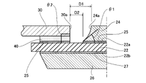
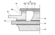
12:半導体素子
14:封止体
20、120:絶縁回路基板
22、122:絶縁基板
24、26、124、126、224:導体膜
25、27、125、127:ろう材
30:信号端子
32:第1電力端子
34:第2電力端子
40:接合層
Claims (12)
- 絶縁体で構成された基板と、
前記基板上の一部に設けられた第1導体膜と、
前記第1導体膜上に配置された半導体素子と、
前記第1導体膜から離れた位置で、前記基板上に接合層を介して接合された外部接続端子と、
を備え、
前記半導体素子は、主電極と信号電極とを有するパワー半導体素子であり、
前記主電極は、前記第1導体膜と電気的に接続されており、前記信号電極は、前記外部接続端子と電気的に接続されており、
前記第1導体膜の厚みは、前記外部接続端子の厚みよりも大きい、
半導体装置。 - 前記外部接続端子は、前記接合層に接する第1区間と、前記第1区間から前記基板の外部へ延びるとともに、前記第1区間よりも厚みの小さい第2区間とを有する、請求項1に記載の半導体装置。
- 絶縁体で構成された基板と、
前記基板上の一部に設けられた第1導体膜と、
前記第1導体膜上に配置された半導体素子と、
前記第1導体膜から離れた位置で、前記基板上に接合層を介して接合された外部接続端子と、
を備え、
前記半導体素子は、主電極と信号電極とを有するパワー半導体素子であり、
前記主電極は、前記第1導体膜と電気的に接続されており、前記信号電極は、前記外部接続端子と電気的に接続されており、
前記外部接続端子は、前記接合層に接する第1区間と、前記第1区間から前記基板の外部へ延びるとともに、前記第1区間よりも厚みの小さい第2区間とを有する、
半導体装置。 - 前記半導体素子の一部は、前記外部接続端子上に位置しており、前記信号電極が前記外部接続端子に接合されている、請求項1から3のいずれか一項に記載の半導体装置。
- 前記外部接続端子は、前記信号電極と対向する部分が、前記信号電極に向けて突出している、請求項1から4のいずれか一項に記載の半導体装置。
- 前記外部接続端子の側面が前記基板と成す角度は、前記第1導体膜の側面が前記基板と成す角度よりも大きい、請求項1から5のいずれか一項に記載の半導体装置。
- 前記半導体素子は、IGBT(Insulated Gate Bipolar Transistor)構造を含むパワー半導体素子であり、
前記主電極は、前記IGBT構造のエミッタ又はコレクタに接続されており、
前記信号電極は、前記IGBT構造のゲートに接続されている、請求項1から6のいずれか一項に記載の半導体装置。 - 前記半導体素子は、MOSFET(Metal-Oxide-Semiconductor Field-Effect Transistor)構造を含むパワー半導体素子であり、
前記主電極は、前記MOSFETのソース又はドレインに接続されており、
前記信号電極は、前記MOSFETのゲートに接続されている、請求項1から6のいずれか一項に記載の半導体装置。 - 前記基板は、セラミック基板である、請求項1から8のいずれか一項に記載の半導体装置。
- 前記第1導体膜は、ろう材を介して前記基板上に接合されている、請求項1から9のいずれか一項に記載の半導体装置。
- 前記基板の前記第1導体膜とは反対側に設けられた第2導体膜をさらに備える、請求項1から10のいずれか一項に記載の半導体装置。
- 半導体装置の製造方法であって、
絶縁体で構成された基板上の導体膜を部分的にエッチングして、前記基板上の一部を覆う第1導体膜を形成する工程と、
前記第1導体膜から離れた位置で、前記基板上に接合層を介して外部接続端子を接合する工程と、
前記第1導体膜上に、主電極と信号電極とを有するパワー半導体素子を、前記主電極が前記第1導体膜に対向するように配置する工程と、
前記パワー半導体素子の前記主電極を、前記第1導体膜に接合する工程と、
前記パワー半導体素子の前記信号電極を、前記基板上に接合された前記外部接続端子へ電気的に接続する工程と、
を備え、
前記配置する工程では、前記信号電極が前記外部接続端子に対向するように、前記パワー半導体素子の一部を前記外部接続端子上に配置し、
前記電気的に接続する工程では、前記接合する工程と並行して、前記信号電極を前記外部接続端子へ接合する、
製造方法。
Priority Applications (4)
| Application Number | Priority Date | Filing Date | Title |
|---|---|---|---|
| JP2018239956A JP7176397B2 (ja) | 2018-12-21 | 2018-12-21 | 半導体装置とその製造方法 |
| US16/693,478 US11201099B2 (en) | 2018-12-21 | 2019-11-25 | Semiconductor device and method of manufacturing the same |
| CN201911319896.9A CN111354710B (zh) | 2018-12-21 | 2019-12-19 | 半导体装置及其制造方法 |
| DE102019135373.4A DE102019135373B4 (de) | 2018-12-21 | 2019-12-20 | Halbleitervorrichtung und Verfahren zum Herstellen derselben |
Applications Claiming Priority (1)
| Application Number | Priority Date | Filing Date | Title |
|---|---|---|---|
| JP2018239956A JP7176397B2 (ja) | 2018-12-21 | 2018-12-21 | 半導体装置とその製造方法 |
Publications (2)
| Publication Number | Publication Date |
|---|---|
| JP2020102544A JP2020102544A (ja) | 2020-07-02 |
| JP7176397B2 true JP7176397B2 (ja) | 2022-11-22 |
Family
ID=70969295
Family Applications (1)
| Application Number | Title | Priority Date | Filing Date |
|---|---|---|---|
| JP2018239956A Active JP7176397B2 (ja) | 2018-12-21 | 2018-12-21 | 半導体装置とその製造方法 |
Country Status (4)
| Country | Link |
|---|---|
| US (1) | US11201099B2 (ja) |
| JP (1) | JP7176397B2 (ja) |
| CN (1) | CN111354710B (ja) |
| DE (1) | DE102019135373B4 (ja) |
Families Citing this family (4)
| Publication number | Priority date | Publication date | Assignee | Title |
|---|---|---|---|---|
| KR102588851B1 (ko) * | 2021-04-14 | 2023-10-16 | 주식회사 아모센스 | 파워모듈 및 그 제조방법 |
| JP7400773B2 (ja) * | 2021-05-27 | 2023-12-19 | 株式会社デンソー | 半導体装置 |
| KR102735483B1 (ko) * | 2021-12-31 | 2024-11-28 | 주식회사 아모센스 | 세라믹 기판 유닛 및 그 제조방법 |
| US20250329659A1 (en) * | 2022-09-09 | 2025-10-23 | Mitsubishi Electric Corporation | Semiconductor device |
Citations (2)
| Publication number | Priority date | Publication date | Assignee | Title |
|---|---|---|---|---|
| JP2013183022A (ja) | 2012-03-01 | 2013-09-12 | Toyota Industries Corp | 半導体装置および半導体装置の製造方法 |
| JP2016174165A (ja) | 2011-12-20 | 2016-09-29 | 株式会社東芝 | 半導体装置 |
Family Cites Families (19)
| Publication number | Priority date | Publication date | Assignee | Title |
|---|---|---|---|---|
| US4538170A (en) | 1983-01-03 | 1985-08-27 | General Electric Company | Power chip package |
| JPH05343591A (ja) | 1992-06-11 | 1993-12-24 | Sumitomo Metal Ind Ltd | リードフレーム及びその製造方法 |
| JP3879150B2 (ja) * | 1996-08-12 | 2007-02-07 | 株式会社デンソー | 半導体装置 |
| JP2007251076A (ja) | 2006-03-20 | 2007-09-27 | Hitachi Ltd | パワー半導体モジュール |
| DE102006034679A1 (de) * | 2006-07-24 | 2008-01-31 | Infineon Technologies Ag | Halbleitermodul mit Leistungshalbleiterchip und passiven Bauelement sowie Verfahren zur Herstellung desselben |
| US7557434B2 (en) | 2006-08-29 | 2009-07-07 | Denso Corporation | Power electronic package having two substrates with multiple electronic components |
| DE102006049949B3 (de) * | 2006-10-19 | 2008-05-15 | Infineon Technologies Ag | Halbleitermodul mit Halbleiterchips auf unterschiedlichen Versorgungspotentialen und Verfahren zur Herstelllung desselben |
| US8164176B2 (en) * | 2006-10-20 | 2012-04-24 | Infineon Technologies Ag | Semiconductor module arrangement |
| KR101493865B1 (ko) * | 2007-11-16 | 2015-02-17 | 페어차일드코리아반도체 주식회사 | 구조가 단순화된 반도체 파워 모듈 패키지 및 그 제조방법 |
| JP5257817B2 (ja) * | 2010-06-15 | 2013-08-07 | 三菱電機株式会社 | 半導体装置 |
| JP2012146760A (ja) | 2011-01-11 | 2012-08-02 | Calsonic Kansei Corp | パワー半導体モジュール |
| CN104126225B (zh) * | 2012-02-14 | 2017-04-12 | 三菱电机株式会社 | 半导体装置 |
| DE112012006656B4 (de) * | 2012-07-05 | 2021-08-05 | Mitsubishi Electric Corporation | Halbleitervorrichtung |
| WO2015045648A1 (ja) * | 2013-09-30 | 2015-04-02 | 富士電機株式会社 | 半導体装置、半導体装置の組み立て方法、半導体装置用部品及び単位モジュール |
| DE102015104990B4 (de) * | 2015-03-31 | 2020-06-04 | Infineon Technologies Austria Ag | Verbindungshalbleitervorrichtung mit einem Abtastlead |
| DE102015104996B4 (de) * | 2015-03-31 | 2020-06-18 | Infineon Technologies Austria Ag | Halbleitervorrichtungen mit Steuer- und Lastleitungen von entgegengesetzter Richtung |
| JP6897141B2 (ja) * | 2017-02-15 | 2021-06-30 | 株式会社デンソー | 半導体装置とその製造方法 |
| JP6809294B2 (ja) * | 2017-03-02 | 2021-01-06 | 三菱電機株式会社 | パワーモジュール |
| JP7260278B2 (ja) * | 2018-10-19 | 2023-04-18 | 現代自動車株式会社 | 半導体サブアセンブリー及び半導体パワーモジュール |
-
2018
- 2018-12-21 JP JP2018239956A patent/JP7176397B2/ja active Active
-
2019
- 2019-11-25 US US16/693,478 patent/US11201099B2/en active Active
- 2019-12-19 CN CN201911319896.9A patent/CN111354710B/zh active Active
- 2019-12-20 DE DE102019135373.4A patent/DE102019135373B4/de active Active
Patent Citations (2)
| Publication number | Priority date | Publication date | Assignee | Title |
|---|---|---|---|---|
| JP2016174165A (ja) | 2011-12-20 | 2016-09-29 | 株式会社東芝 | 半導体装置 |
| JP2013183022A (ja) | 2012-03-01 | 2013-09-12 | Toyota Industries Corp | 半導体装置および半導体装置の製造方法 |
Also Published As
| Publication number | Publication date |
|---|---|
| CN111354710B (zh) | 2023-08-04 |
| DE102019135373B4 (de) | 2024-07-11 |
| US20200203252A1 (en) | 2020-06-25 |
| CN111354710A (zh) | 2020-06-30 |
| DE102019135373A1 (de) | 2020-06-25 |
| JP2020102544A (ja) | 2020-07-02 |
| US11201099B2 (en) | 2021-12-14 |
Similar Documents
| Publication | Publication Date | Title |
|---|---|---|
| US7456492B2 (en) | Semiconductor device having semiconductor element, insulation substrate and metal electrode | |
| JP7176397B2 (ja) | 半導体装置とその製造方法 | |
| JP4885046B2 (ja) | 電力用半導体モジュール | |
| JP7074046B2 (ja) | 半導体装置とその製造方法 | |
| JP2007073743A (ja) | 半導体装置 | |
| CN113039636A (zh) | 功率半导体装置 | |
| CN111276447A (zh) | 双侧冷却功率模块及其制造方法 | |
| CN102437138A (zh) | 半导体装置 | |
| JP7124474B2 (ja) | 半導体装置 | |
| WO2023149144A1 (ja) | 半導体装置 | |
| CN115206919A (zh) | 半导体装置 | |
| JP5217015B2 (ja) | 電力変換装置及びその製造方法 | |
| JP2019083294A (ja) | 半導体装置とその製造方法 | |
| JP7163583B2 (ja) | 半導体装置 | |
| JP2019083292A (ja) | 半導体装置 | |
| JP2006190728A (ja) | 電力用半導体装置 | |
| JP2017054855A (ja) | 半導体装置、及び半導体パッケージ | |
| CN111599781A (zh) | 半导体装置 | |
| US12581969B2 (en) | Semiconductor device | |
| CN115206905B (zh) | 半导体装置和使用该半导体装置的半导体模块 | |
| JP2021034701A (ja) | 半導体装置 | |
| JP7180533B2 (ja) | 半導体装置 | |
| WO2024024067A1 (ja) | 電力変換装置、電力変換装置の製造方法 | |
| JP2021111719A (ja) | 半導体装置 | |
| JP2014033125A (ja) | 半導体装置及び半導体装置の製造方法 |
Legal Events
| Date | Code | Title | Description |
|---|---|---|---|
| A711 | Notification of change in applicant |
Free format text: JAPANESE INTERMEDIATE CODE: A711 Effective date: 20200401 |
|
| A621 | Written request for application examination |
Free format text: JAPANESE INTERMEDIATE CODE: A621 Effective date: 20210520 |
|
| A977 | Report on retrieval |
Free format text: JAPANESE INTERMEDIATE CODE: A971007 Effective date: 20220330 |
|
| A131 | Notification of reasons for refusal |
Free format text: JAPANESE INTERMEDIATE CODE: A131 Effective date: 20220412 |
|
| A521 | Request for written amendment filed |
Free format text: JAPANESE INTERMEDIATE CODE: A523 Effective date: 20220603 |
|
| TRDD | Decision of grant or rejection written | ||
| A01 | Written decision to grant a patent or to grant a registration (utility model) |
Free format text: JAPANESE INTERMEDIATE CODE: A01 Effective date: 20221011 |
|
| A61 | First payment of annual fees (during grant procedure) |
Free format text: JAPANESE INTERMEDIATE CODE: A61 Effective date: 20221024 |
|
| R151 | Written notification of patent or utility model registration |
Ref document number: 7176397 Country of ref document: JP Free format text: JAPANESE INTERMEDIATE CODE: R151 |
|
| R250 | Receipt of annual fees |
Free format text: JAPANESE INTERMEDIATE CODE: R250 |