JP7176397B2 - Semiconductor device and its manufacturing method - Google Patents
Semiconductor device and its manufacturing method Download PDFInfo
- Publication number
- JP7176397B2 JP7176397B2 JP2018239956A JP2018239956A JP7176397B2 JP 7176397 B2 JP7176397 B2 JP 7176397B2 JP 2018239956 A JP2018239956 A JP 2018239956A JP 2018239956 A JP2018239956 A JP 2018239956A JP 7176397 B2 JP7176397 B2 JP 7176397B2
- Authority
- JP
- Japan
- Prior art keywords
- conductor film
- external connection
- substrate
- semiconductor element
- connection terminal
- Prior art date
- Legal status (The legal status is an assumption and is not a legal conclusion. Google has not performed a legal analysis and makes no representation as to the accuracy of the status listed.)
- Active
Links
Images


Classifications
-
- H—ELECTRICITY
- H10—SEMICONDUCTOR DEVICES; ELECTRIC SOLID-STATE DEVICES NOT OTHERWISE PROVIDED FOR
- H10W—GENERIC PACKAGES, INTERCONNECTIONS, CONNECTORS OR OTHER CONSTRUCTIONAL DETAILS OF DEVICES COVERED BY CLASS H10
- H10W40/00—Arrangements for thermal protection or thermal control
- H10W40/20—Arrangements for cooling
- H10W40/25—Arrangements for cooling characterised by their materials
- H10W40/255—Arrangements for cooling characterised by their materials having a laminate or multilayered structure, e.g. direct bond copper [DBC] ceramic substrates
-
- H—ELECTRICITY
- H10—SEMICONDUCTOR DEVICES; ELECTRIC SOLID-STATE DEVICES NOT OTHERWISE PROVIDED FOR
- H10W—GENERIC PACKAGES, INTERCONNECTIONS, CONNECTORS OR OTHER CONSTRUCTIONAL DETAILS OF DEVICES COVERED BY CLASS H10
- H10W40/00—Arrangements for thermal protection or thermal control
- H10W40/01—Manufacture or treatment
- H10W40/03—Manufacture or treatment of arrangements for cooling
- H10W40/037—Assembling together parts thereof
-
- H—ELECTRICITY
- H10—SEMICONDUCTOR DEVICES; ELECTRIC SOLID-STATE DEVICES NOT OTHERWISE PROVIDED FOR
- H10W—GENERIC PACKAGES, INTERCONNECTIONS, CONNECTORS OR OTHER CONSTRUCTIONAL DETAILS OF DEVICES COVERED BY CLASS H10
- H10W40/00—Arrangements for thermal protection or thermal control
- H10W40/20—Arrangements for cooling
- H10W40/22—Arrangements for cooling characterised by their shape, e.g. having conical or cylindrical projections
- H10W40/226—Arrangements for cooling characterised by their shape, e.g. having conical or cylindrical projections characterised by projecting parts, e.g. fins to increase surface area
- H10W40/228—Arrangements for cooling characterised by their shape, e.g. having conical or cylindrical projections characterised by projecting parts, e.g. fins to increase surface area the projecting parts being wire-shaped or pin-shaped
-
- H—ELECTRICITY
- H10—SEMICONDUCTOR DEVICES; ELECTRIC SOLID-STATE DEVICES NOT OTHERWISE PROVIDED FOR
- H10W—GENERIC PACKAGES, INTERCONNECTIONS, CONNECTORS OR OTHER CONSTRUCTIONAL DETAILS OF DEVICES COVERED BY CLASS H10
- H10W40/00—Arrangements for thermal protection or thermal control
- H10W40/70—Fillings or auxiliary members in containers or in encapsulations for thermal protection or control
- H10W40/77—Auxiliary members characterised by their shape
- H10W40/778—Auxiliary members characterised by their shape in encapsulations
-
- H—ELECTRICITY
- H10—SEMICONDUCTOR DEVICES; ELECTRIC SOLID-STATE DEVICES NOT OTHERWISE PROVIDED FOR
- H10W—GENERIC PACKAGES, INTERCONNECTIONS, CONNECTORS OR OTHER CONSTRUCTIONAL DETAILS OF DEVICES COVERED BY CLASS H10
- H10W70/00—Package substrates; Interposers; Redistribution layers [RDL]
- H10W70/60—Insulating or insulated package substrates; Interposers; Redistribution layers
- H10W70/62—Insulating or insulated package substrates; Interposers; Redistribution layers characterised by their interconnections
- H10W70/65—Shapes or dispositions of interconnections
- H10W70/658—Shapes or dispositions of interconnections for devices provided for in groups H10D8/00 - H10D48/00
-
- H—ELECTRICITY
- H10—SEMICONDUCTOR DEVICES; ELECTRIC SOLID-STATE DEVICES NOT OTHERWISE PROVIDED FOR
- H10W—GENERIC PACKAGES, INTERCONNECTIONS, CONNECTORS OR OTHER CONSTRUCTIONAL DETAILS OF DEVICES COVERED BY CLASS H10
- H10W72/00—Interconnections or connectors in packages
- H10W72/071—Connecting or disconnecting
- H10W72/073—Connecting or disconnecting of die-attach connectors
-
- H—ELECTRICITY
- H10—SEMICONDUCTOR DEVICES; ELECTRIC SOLID-STATE DEVICES NOT OTHERWISE PROVIDED FOR
- H10W—GENERIC PACKAGES, INTERCONNECTIONS, CONNECTORS OR OTHER CONSTRUCTIONAL DETAILS OF DEVICES COVERED BY CLASS H10
- H10W90/00—Package configurations
- H10W90/401—Package configurations characterised by multiple insulating or insulated package substrates, interposers or RDLs
-
- H—ELECTRICITY
- H10—SEMICONDUCTOR DEVICES; ELECTRIC SOLID-STATE DEVICES NOT OTHERWISE PROVIDED FOR
- H10W—GENERIC PACKAGES, INTERCONNECTIONS, CONNECTORS OR OTHER CONSTRUCTIONAL DETAILS OF DEVICES COVERED BY CLASS H10
- H10W90/00—Package configurations
- H10W90/701—Package configurations characterised by the relative positions of pads or connectors relative to package parts
-
- H—ELECTRICITY
- H10—SEMICONDUCTOR DEVICES; ELECTRIC SOLID-STATE DEVICES NOT OTHERWISE PROVIDED FOR
- H10W—GENERIC PACKAGES, INTERCONNECTIONS, CONNECTORS OR OTHER CONSTRUCTIONAL DETAILS OF DEVICES COVERED BY CLASS H10
- H10W99/00—Subject matter not provided for in other groups of this subclass
-
- H—ELECTRICITY
- H10—SEMICONDUCTOR DEVICES; ELECTRIC SOLID-STATE DEVICES NOT OTHERWISE PROVIDED FOR
- H10W—GENERIC PACKAGES, INTERCONNECTIONS, CONNECTORS OR OTHER CONSTRUCTIONAL DETAILS OF DEVICES COVERED BY CLASS H10
- H10W70/00—Package substrates; Interposers; Redistribution layers [RDL]
- H10W70/40—Leadframes
- H10W70/421—Shapes or dispositions
- H10W70/424—Cross-sectional shapes
-
- H—ELECTRICITY
- H10—SEMICONDUCTOR DEVICES; ELECTRIC SOLID-STATE DEVICES NOT OTHERWISE PROVIDED FOR
- H10W—GENERIC PACKAGES, INTERCONNECTIONS, CONNECTORS OR OTHER CONSTRUCTIONAL DETAILS OF DEVICES COVERED BY CLASS H10
- H10W72/00—Interconnections or connectors in packages
- H10W72/071—Connecting or disconnecting
- H10W72/073—Connecting or disconnecting of die-attach connectors
- H10W72/07351—Connecting or disconnecting of die-attach connectors characterised by changes in properties of the die-attach connectors during connecting
- H10W72/07354—Connecting or disconnecting of die-attach connectors characterised by changes in properties of the die-attach connectors during connecting changes in dispositions
-
- H—ELECTRICITY
- H10—SEMICONDUCTOR DEVICES; ELECTRIC SOLID-STATE DEVICES NOT OTHERWISE PROVIDED FOR
- H10W—GENERIC PACKAGES, INTERCONNECTIONS, CONNECTORS OR OTHER CONSTRUCTIONAL DETAILS OF DEVICES COVERED BY CLASS H10
- H10W72/00—Interconnections or connectors in packages
- H10W72/30—Die-attach connectors
- H10W72/341—Dispositions of die-attach connectors, e.g. layouts
- H10W72/347—Dispositions of multiple die-attach connectors
-
- H—ELECTRICITY
- H10—SEMICONDUCTOR DEVICES; ELECTRIC SOLID-STATE DEVICES NOT OTHERWISE PROVIDED FOR
- H10W—GENERIC PACKAGES, INTERCONNECTIONS, CONNECTORS OR OTHER CONSTRUCTIONAL DETAILS OF DEVICES COVERED BY CLASS H10
- H10W72/00—Interconnections or connectors in packages
- H10W72/851—Dispositions of multiple connectors or interconnections
- H10W72/874—On different surfaces
- H10W72/884—Die-attach connectors and bond wires
-
- H—ELECTRICITY
- H10—SEMICONDUCTOR DEVICES; ELECTRIC SOLID-STATE DEVICES NOT OTHERWISE PROVIDED FOR
- H10W—GENERIC PACKAGES, INTERCONNECTIONS, CONNECTORS OR OTHER CONSTRUCTIONAL DETAILS OF DEVICES COVERED BY CLASS H10
- H10W72/00—Interconnections or connectors in packages
- H10W72/90—Bond pads, in general
- H10W72/921—Structures or relative sizes of bond pads
- H10W72/926—Multiple bond pads having different sizes
-
- H—ELECTRICITY
- H10—SEMICONDUCTOR DEVICES; ELECTRIC SOLID-STATE DEVICES NOT OTHERWISE PROVIDED FOR
- H10W—GENERIC PACKAGES, INTERCONNECTIONS, CONNECTORS OR OTHER CONSTRUCTIONAL DETAILS OF DEVICES COVERED BY CLASS H10
- H10W72/00—Interconnections or connectors in packages
- H10W72/90—Bond pads, in general
- H10W72/941—Dispositions of bond pads
- H10W72/944—Dispositions of multiple bond pads
-
- H—ELECTRICITY
- H10—SEMICONDUCTOR DEVICES; ELECTRIC SOLID-STATE DEVICES NOT OTHERWISE PROVIDED FOR
- H10W—GENERIC PACKAGES, INTERCONNECTIONS, CONNECTORS OR OTHER CONSTRUCTIONAL DETAILS OF DEVICES COVERED BY CLASS H10
- H10W74/00—Encapsulations, e.g. protective coatings
Landscapes
- Internal Circuitry In Semiconductor Integrated Circuit Devices (AREA)
- Chemical & Material Sciences (AREA)
- Engineering & Computer Science (AREA)
- Ceramic Engineering (AREA)
- Cooling Or The Like Of Semiconductors Or Solid State Devices (AREA)
- Semiconductor Integrated Circuits (AREA)
Description
本明細書が開示する技術は、半導体装置とその製造方法に関する。 The technology disclosed in this specification relates to a semiconductor device and a method for manufacturing the same.
特許文献1に、半導体装置が開示されている。この半導体装置は、セラミック基板と、セラミック基板上に配置された半導体素子と、半導体素子から離れた位置で、基板上に接合された外部接続端子とを備える。外部接続端子は、セラミック基板上に設けられた導体膜(導体配線パターン)を介して、半導体素子と電気的に接続されている。 A semiconductor device is disclosed in Japanese Patent Laid-Open No. 2002-200012. This semiconductor device includes a ceramic substrate, a semiconductor element arranged on the ceramic substrate, and external connection terminals joined to the substrate at a position separated from the semiconductor element. The external connection terminals are electrically connected to the semiconductor element via a conductor film (conductor wiring pattern) provided on the ceramic substrate.
上記した半導体装置では、半導体素子と導体膜との間が、ボンディングワイヤを介して接続されている。これに対して、ボンディングワイヤを省略し、導体膜と半導体素子との間を直接的に接続すれば、半導体装置の小型化を図ることができる。特に、セラミック基板上には、複数の導体膜を独立して(即ち、互いに離間させて)形成することができる。従って、半導体素子が複数の電極を有する場合は、各々の電極に対応する導体膜を、個別に設けることができる。 In the semiconductor device described above, the semiconductor element and the conductor film are connected via bonding wires. On the other hand, if the bonding wire is omitted and the conductor film and the semiconductor element are directly connected, the size of the semiconductor device can be reduced. In particular, a plurality of conductor films can be formed independently (that is, separated from each other) on a ceramic substrate. Therefore, when a semiconductor element has a plurality of electrodes, a conductor film corresponding to each electrode can be provided individually.
セラミック基板上に複数の導体膜を設ける場合は、隣り合う導体膜の間に一定の間隔を設けて、それらの間の絶縁性を確保する必要がある。この点に関して、導体膜がエッチング(特に、ウェットエッチング)によって形成されると、導体膜の周縁に沿って延びる側面は、裾広がりの形状を有する。従って、複数の導体膜の配列を設計するときは、そのような側面の形状も考慮して、隣り合う導体膜の間に大きな間隔を設ける必要が生じる。 When a plurality of conductor films are provided on a ceramic substrate, it is necessary to provide a certain interval between adjacent conductor films to ensure insulation therebetween. In this regard, when the conductor film is formed by etching (in particular, wet etching), the side surfaces extending along the peripheral edge of the conductor film have a widening shape. Therefore, when designing the arrangement of a plurality of conductor films, it is necessary to provide a large gap between adjacent conductor films in consideration of such side shapes.
一般に、導体膜の厚みが大きくなるほど、導体膜の熱容量が増大することによって、半導体素子の温度上昇が抑制される。そのことから、導体膜にはある程度の厚みを持たせることが好ましい。その一方で、導体膜の厚みが大きくなるほど、その側面に形成される裾広がりの幅も大きくなるので、隣り合う導体膜の間に必要とされる間隔も大きくなる。上述したように、導体膜の厚みが大きくなるほど、隣り合う導体膜の間に必要とされる間隔も大きくなり、半導体装置の大型化を招いてしまう。以上の実情を考慮し、本明細書は、半導体装置の大型化を招くことなく、半導体素子の温度上昇を抑制し得る技術を提供する。 In general, as the thickness of the conductor film increases, the heat capacity of the conductor film increases, thereby suppressing the temperature rise of the semiconductor element. Therefore, it is preferable to give the conductor film a certain thickness. On the other hand, as the thickness of the conductor film increases, the width of the flare formed on the side surface also increases, so the required space between the adjacent conductor films also increases. As described above, the greater the thickness of the conductor film, the greater the space required between adjacent conductor films, leading to an increase in the size of the semiconductor device. In consideration of the above circumstances, the present specification provides a technique capable of suppressing the temperature rise of a semiconductor element without increasing the size of the semiconductor device.
本明細書が開示する半導体装置は、絶縁体で構成された基板と、基板上の一部に設けられた第1導体膜と、第1導体膜上に配置された半導体素子と、第1導体膜から離れた位置で、基板上に接合層を介して接合された外部接続端子とを備える。半導体素子は、主電極と信号電極とを有するパワー半導体素子であり、その主電極は第1導体膜に接合されており、その信号電極は外部接続端子と電気的に接続されている。 A semiconductor device disclosed in this specification includes a substrate made of an insulator, a first conductor film provided on a portion of the substrate, a semiconductor element disposed on the first conductor film, and a first conductor. and an external connection terminal bonded to the substrate via a bonding layer at a position away from the film. The semiconductor element is a power semiconductor element having a main electrode and a signal electrode, the main electrode being joined to the first conductor film, and the signal electrode being electrically connected to the external connection terminal.
上記した半導体装置では、絶縁体で構成された基板上に、第1導体膜が設けられているとともに、外部接続端子が接合層を介して接合されている。そして、第1導体膜には、半導体素子の主電極が接合されており、外部接続端子には、半導体素子の信号電極が電気的に接続されている。即ち、半導体素子の二つの電極のうち、信号電極については、基板上の導体膜を介することなく、外部接続端子に接続されている。外部接続端子は、基板上に接合層を介して接合される部材なので、例えばプレス加工といった機械加工によって製造可能であり、その形状を正確に管理することができる。従って、第1導体膜がエッチングによって形成される場合でも、外部接続端子と第1導体膜との間に必要とされる間隔は、エッチングによって形成される二つの導体膜の間に必要とされる間隔と比較すれば、小さくて足りる。これにより、第1導体膜を比較的に厚く形成する場合でも、半導体装置の大型化を避けることができる。 In the semiconductor device described above, the first conductor film is provided on the substrate made of an insulator, and the external connection terminals are bonded via the bonding layer. A main electrode of the semiconductor element is joined to the first conductor film, and a signal electrode of the semiconductor element is electrically connected to the external connection terminal. That is, of the two electrodes of the semiconductor element, the signal electrode is connected to the external connection terminal without interposing the conductor film on the substrate. Since the external connection terminal is a member that is bonded to the substrate via the bonding layer, it can be manufactured by mechanical processing such as press working, and its shape can be controlled accurately. Therefore, even when the first conductor film is formed by etching, the space required between the external connection terminal and the first conductor film is required between the two conductor films formed by etching. Compared with the interval, it is small enough. As a result, even when the first conductor film is formed relatively thick, it is possible to avoid an increase in the size of the semiconductor device.
ここで、半導体装置のさらなる小型化を図るために、主電極に対する第1導体膜についても、基板上に接合層を介して接合される別部材に変更することが考えられる。しかしながら、その別部材と基板との間に接合層が介在することで、主電極から放出される半導体素子の熱が、接合層を介して外部へ放熱されることになり、半導体素子の温度上昇を招くおそれがある。そのことから、上記した半導体装置では、半導体素子の放熱に大きく寄与する主電極に対しては、放熱性に優れる第1導体膜が用意されており、これによって半導体素子の温度上昇が抑制される。それに対して、信号電極については、半導体素子の放熱における寄与度が小さい。従って、信号電極から放出される半導体素子の熱が、接合層を介して外部へ放熱される構成であっても、半導体素子の温度に与える影響は無視又は許容することができる。 Here, in order to achieve further miniaturization of the semiconductor device, it is conceivable to change the first conductor film for the main electrode to a separate member that is bonded to the substrate via the bonding layer. However, since the bonding layer is interposed between the separate member and the substrate, the heat of the semiconductor element emitted from the main electrode is radiated to the outside through the bonding layer, and the temperature of the semiconductor element rises. may lead to For this reason, in the semiconductor device described above, the first conductor film having excellent heat dissipation properties is prepared for the main electrode that greatly contributes to the heat dissipation of the semiconductor element, thereby suppressing the temperature rise of the semiconductor element. . On the other hand, the contribution of the signal electrode to the heat dissipation of the semiconductor element is small. Therefore, even if the heat of the semiconductor element emitted from the signal electrode is dissipated to the outside through the bonding layer, the influence on the temperature of the semiconductor element can be ignored or allowed.
本技術の一実施形態において、半導体素子の一部は、外部接続端子上に位置しており、信号電極が外部接続端子に接合されていてもよい。この場合、一例ではあるが、信号電極と外部接続端子との間は、はんだ材といった導電性の接合材を介して接合されてもよい。また、信号電極と外部接続端子との間には、スペーサといった他の部材が介して接合されてもよい。このような構成によると、外部接続端子が第1導体膜に近接して配置されるので、半導体装置の小型化を効果的に図ることができる。但し、他の実施形態として、信号電極と外部接続端子とは離れて配置され、信号電極と外部接続端子との間がボンディングワイヤを介して電気的に接続されてもよい。 In one embodiment of the present technology, a portion of the semiconductor element may be located on the external connection terminal, and the signal electrode may be bonded to the external connection terminal. In this case, although it is an example, the signal electrode and the external connection terminal may be joined via a conductive joining material such as a solder material. Further, another member such as a spacer may be interposed between the signal electrode and the external connection terminal. According to such a configuration, since the external connection terminals are arranged close to the first conductor film, it is possible to effectively reduce the size of the semiconductor device. However, as another embodiment, the signal electrodes and the external connection terminals may be arranged separately, and the signal electrodes and the external connection terminals may be electrically connected via bonding wires.
本明細書は、半導体装置の製造方法も開示する。この製造方法は、例えば、上記した半導体装置を製造することができる。この製造方法は、絶縁体で構成された基板上の導体膜を部分的にエッチングして、基板上の一部を覆う第1導体膜を形成する工程と、第1導体膜から離れた位置で、基板上に接合層を介して外部接続端子を接合する工程と、第1導体膜上に、主電極と信号電極とを有するパワー半導体素子を、主電極が第1導体膜に対向するように配置する工程と、パワー半導体素子の主電極を、第1導体膜に接合する工程と、パワー半導体素子の信号電極を、基板上に接合された外部接続端子へ電気的に接続する工程とを備える。 This specification also discloses a method of manufacturing a semiconductor device. This manufacturing method can manufacture, for example, the semiconductor device described above. This manufacturing method includes steps of partially etching a conductor film on a substrate made of an insulator to form a first conductor film covering a portion of the substrate; a step of bonding an external connection terminal onto a substrate via a bonding layer; and disposing a power semiconductor element having a main electrode and a signal electrode on a first conductor film such that the main electrode faces the first conductor film. bonding the main electrode of the power semiconductor element to the first conductor film; and electrically connecting the signal electrode of the power semiconductor element to the external connection terminal bonded on the substrate. .
上記した製造方法において、第1導体膜上にパワー半導体素子を配置する工程では、信号電極が外部接続端子に対向するように、パワー半導体素子の一部を外部接続端子上に配置してもよい。この場合、電気的に接続する工程では、前記接合する工程と並行して、信号電極を外部接続端子へ接合してもよい。 In the manufacturing method described above, in the step of disposing the power semiconductor element on the first conductor film, part of the power semiconductor element may be disposed on the external connection terminal such that the signal electrode faces the external connection terminal. . In this case, in the electrically connecting step, the signal electrode may be bonded to the external connection terminal in parallel with the bonding step.
本技術の一実施形態において、外部接続端子は、信号電極と対向する部分が、信号電極に向けて突出していてもよい。このような構成によると、外部接続端子と信号電極との間の距離を適切に調整することができ、例えばスペーサといった別の部材を必要とすることなく、外部接続端子と信号電極との間を正しく接合することができる。 In one embodiment of the present technology, the portion of the external connection terminal facing the signal electrode may protrude toward the signal electrode. With such a configuration, the distance between the external connection terminal and the signal electrode can be appropriately adjusted, and the distance between the external connection terminal and the signal electrode can be adjusted without requiring a separate member such as a spacer. can be joined correctly.
本技術の一実施形態において、外部接続端子の側面が基板と成す角度は、第1導体膜の側面が基板と成す角度より大きくてもよい。前述したように、第1導体膜がエッチングによって形成されると、第1導体膜の周縁に沿って延びる側面は、裾広がりの形状を有することが多い。第1導体膜の側面が裾広がりの形状を有していると、第1導体膜の側面が基板と成す角度は、90度よりも小さくなる。このような第1導体膜に対して、外部接続端子の側面も裾広がりの形状を有していると、基板上における第1導体膜と外部接続端子との間の距離(いわゆる沿面距離)が短くなるので、第1導体膜と外部接続端子との間の絶縁性が低下する。言い換えると、必要とされる絶縁性を確保するためには、第1導体膜と外部接続端子との間隔を大きくする必要が生じる。そのことから、外部接続端子の側面は、裾広がりの形状を有さないことが好ましく、仮に裾広がりの形状を有するとしても、その程度は小さいことが好ましい。即ち、外部接続端子の側面が基板と成す角度は、90度であるとよく、あるいは、第1導体膜の側面が基板と成す角度よりも大きくするとよい。 In one embodiment of the present technology, the angle formed between the side surface of the external connection terminal and the substrate may be greater than the angle formed between the side surface of the first conductor film and the substrate. As described above, when the first conductor film is formed by etching, the side surface extending along the periphery of the first conductor film often has a widening shape. When the side surface of the first conductor film has a shape that spreads toward the bottom, the angle formed between the side surface of the first conductor film and the substrate is smaller than 90 degrees. With respect to such a first conductor film, if the side surface of the external connection terminal also has a shape that spreads toward the bottom, the distance (so-called creepage distance) between the first conductor film and the external connection terminal on the substrate increases. Since it is shortened, the insulation between the first conductor film and the external connection terminal is deteriorated. In other words, it becomes necessary to increase the distance between the first conductor film and the external connection terminal in order to ensure the required insulation. For this reason, it is preferable that the side surface of the external connection terminal does not have a shape that spreads toward the bottom. In other words, the angle formed by the side surface of the external connection terminal and the substrate is preferably 90 degrees, or the angle formed by the side surface of the first conductor film and the substrate is preferably larger than the angle formed by the substrate.
本技術の一実施形態において、第1導体膜の厚みは、外部接続端子の厚みより大きくてもよい。第1導体膜の厚みが大きくなるほど、第1導体膜の熱容量が増大することによって、半導体素子の温度上昇が抑制される。特に、第1導体膜は、半導体素子の主電極に接合されており、半導体素子から多くの熱を受け取ることができる。従って、外部接続端子の厚みを大きくするよりも、第1導体膜の厚みを大きくすることで、半導体素子の温度上昇を効果的に抑制することができる。 In one embodiment of the present technology, the thickness of the first conductor film may be greater than the thickness of the external connection terminal. As the thickness of the first conductor film increases, the heat capacity of the first conductor film increases, thereby suppressing the temperature rise of the semiconductor element. In particular, the first conductor film is joined to the main electrode of the semiconductor element and can receive a large amount of heat from the semiconductor element. Therefore, rather than increasing the thickness of the external connection terminal, increasing the thickness of the first conductor film can effectively suppress the temperature rise of the semiconductor element.
本技術の一実施形態において、外部接続端子は、接合層に接する第1区間と、第1区間から基板の外部へ延びるとともに、第1区間よりも厚みの小さい第2区間とを有してもよい。このような構成によると、外部接続端子が、基板の周縁において基板と接触することがない。これにより、外部接続端子と、基板の反対側に設けられた他の部材との間で、基板に沿った沿面距離を長くすることができる。 In one embodiment of the present technology, the external connection terminal may have a first section in contact with the bonding layer and a second section extending from the first section to the outside of the substrate and having a smaller thickness than the first section. good. According to such a configuration, the external connection terminal does not come into contact with the substrate at the periphery of the substrate. This makes it possible to increase the creepage distance along the board between the external connection terminal and another member provided on the opposite side of the board.
本技術の一実施形態において、半導体素子は、IGBT(Insulated Gate Bipolar Transistor)構造を含むパワー半導体素子であってよい。この場合、半導体素子の主電極は、IGBT構造のエミッタ又はコレクタに接続されており、半導体素子の信号電極は、IGBT構造のゲートに接続されていてもよい。あるいは、半導体素子は、MOSFET(Metal-Oxide-Semiconductor Field-Effect Transistor)構造を含むパワー半導体素子であってもよい。この場合、半導体素子の主電極は、MOSFETのソース又はドレインに接続されており、半導体素子の信号電極は、MOSFETのゲートに接続されていてもよい。 In one embodiment of the present technology, the semiconductor element may be a power semiconductor element including an IGBT (Insulated Gate Bipolar Transistor) structure. In this case, the main electrode of the semiconductor element may be connected to the emitter or collector of the IGBT structure and the signal electrode of the semiconductor element may be connected to the gate of the IGBT structure. Alternatively, the semiconductor device may be a power semiconductor device including a MOSFET (Metal-Oxide-Semiconductor Field-Effect Transistor) structure. In this case, the main electrode of the semiconductor element may be connected to the source or drain of the MOSFET, and the signal electrode of the semiconductor element may be connected to the gate of the MOSFET.
本技術の一実施形態において、基板はセラミック基板であってもよい。加えて、又は代えて、第1導体膜は、ろう材を介して基板上に接合されていてもよい。この場合、ろう材は、活性金属ろうであってもよい。即ち、基板及び第1導体膜は、AMB(Active Metal Brazing)法を用いて形成された基板、例えば、AMC(Active Metal Brazed Copper)基板であってもよい。 In one embodiment of the present technology, the substrate may be a ceramic substrate. Additionally or alternatively, the first conductor film may be bonded onto the substrate via a brazing material. In this case, the brazing material may be an active metal brazing material. That is, the substrate and the first conductor film may be a substrate formed using an AMB (Active Metal Brazing) method, such as an AMC (Active Metal Brazed Copper) substrate.
本技術の一実施形態において、半導体装置は、基板の第1導体膜とは反対側に設けられた第2導体膜をさらに備えてもよい。このような構成によると、第2導体膜の熱容量によって、半導体素子の温度上昇を抑制することができる。また、基板の両面に導体膜が存在することで、基板に生じる熱変形(特に、反り)も抑制される。 In one embodiment of the present technology, the semiconductor device may further include a second conductor film provided on the opposite side of the substrate from the first conductor film. According to such a configuration, it is possible to suppress the temperature rise of the semiconductor element due to the heat capacity of the second conductor film. In addition, since the conductor films are present on both surfaces of the substrate, thermal deformation (in particular, warpage) of the substrate is suppressed.
図面を参照して、実施例の半導体装置10について説明する。半導体装置10は、例えば電気自動車の電力制御装置に採用され、コンバータやインバータといった電力変換回路の少なくとも一部を構成することができる。ここでいう電気自動車は、車輪を駆動するモータを有する自動車を広く意味し、例えば、外部の電力によって充電される電気自動車、モータに加えてエンジンを有するハイブリッド車、及び燃料電池を電源とする燃料電池車等を含む。
A
図1-図3に示すように、半導体装置10は、半導体素子12と、半導体素子12を封止する封止体14とを備える。封止体14は、絶縁性の材料で構成されている。特に限定されないが、本実施例における封止体14は、例えばエポキシ樹脂といった、封止用材料で構成されている。封止体14は、概して板形状を有している。なお、本願に添付された図面では、図示明瞭化のために、封止体14の断面に付されるべきハッチングが省略されている。
As shown in FIGS. 1 to 3, the
半導体素子12は、パワー半導体素子であって、半導体基板12aと、複数の電極12b、12c、12dとを有する。複数の電極12b、12c、12dには、電力回路に接続される第1主電極12b及び第2主電極12cと、信号回路に接続される複数の信号電極12dとが含まれる。特に限定されないが、半導体素子12はスイッチング素子であり、第1主電極12bと第2主電極12cとの間を導通及び遮断することができる。第1主電極12b及び複数の信号電極12dは、半導体基板12aの一方の表面に位置しており、第2主電極12cは、半導体基板12aの他方の表面に位置している。
The
特に限定されないが、本実施例における半導体素子12は、IGBT(Insulated Gate Bipolar Transistor)構造12eを有している。第1主電極12bは、IGBT構造12eのエミッタに接続されており、第2主電極12cは、IGBT構造12eのコレクタに接続されており、信号電極12dは、IGBT構造12eのゲートに接続されている。加えて、半導体素子12は、IGBT構造12eと並列に接続されたダイオード構造12fを有している。第1主電極12bは、ダイオード構造12fのアノードに接続されており、第2主電極12cは、ダイオード構造12fのカソードに接続されている。なお、他の実施形態として、半導体素子12は、MOSFET(Metal-Oxide-Semiconductor Field-Effect Transistor)構造を有してもよい。この場合、第1主電極12bは、MOSFET構造のソースに接続され、第2主電極12cは、MOSFET構造のドレインに接続され、信号電極12dは、MOSFET構造のゲートに接続されている。
Although not particularly limited, the
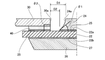
半導体装置10は、絶縁回路基板20をさらに備える。絶縁回路基板20は、絶縁体で構成された絶縁基板22と、絶縁基板22の一方の表面22aに設けられた第1導体膜24と、絶縁基板22の他方の表面22bに設けられた第2導体膜26とを備える。第1導体膜24と第2導体膜26は、それぞれろう材25、27を介して絶縁基板22に接合されている。第1導体膜24は、絶縁基板22上の一部に設けられており、第1導体膜24の面積は、第2導体膜26の面積よりも小さい。第1導体膜24は、封止体14の内部に位置しており、第2導体膜26は、封止体14の表面に露出している。これにより、絶縁回路基板20は、封止体14の内部の熱(特に、半導体素子12の熱)を、封止体14の外部へ放熱する放熱板としても機能する。
The
第1導体膜24上には、半導体素子12が配置されている。半導体素子12の第1主電極12bは、第1導体膜24に対向しており、はんだ層42を介して接合されている。これにより、半導体素子12の第1主電極12bは、第1導体膜24に対して電気的に接続されている。また、半導体素子12の第1主電極12bは、第1導体膜24に対して熱的にも接続されている。なお、第1主電極12bと第1導体膜24との間は、はんだ層42に限られず、導電性を有する他の種類の接合層を介して接合されてもよい。また、第1主電極12bと第1導体膜24との間には、例えば導体スペーサといった他の部材が、必要に応じて介挿されてもよい。
A
本実施例における絶縁基板22は、セラミック基板であり、例えば酸化アルミニウム、窒化シリコン、窒化アルミニウムといった、セラミックで構成されている。第1導体膜24と第2導体膜26は、金属膜であり、例えば銅又はアルミニウムといった金属で構成されている。前述したように、第1導体膜24と第2導体膜26は、それぞれろう材25、27を介して絶縁基板22に接合されている。ろう材25、27は、活性金属ろう材であり、例えば銀及び銅を主たる成分とするろう材に、チタンといった活性金属が添加されている。なお、この種の絶縁回路基板20は、AMC(Active Metal Brazed Copper)基板とも称される。但し、絶縁回路基板20には、AMC基板に限定されず、例えばDBC(Direct Bonded Copper)基板やDBA(Direct Bonded Aluminum)基板を採用することもできる。
The insulating
一例ではあるが、絶縁基板22の厚みは、0.1~1.0ミリメートルであってもよく、第1導体膜24及び第2導体膜26の厚みは、0.05~1.0ミリメートルであってもよい。また、第1導体膜24及び第2導体膜26の厚みは、絶縁基板22の厚みよりも大きくてもよい。第1導体膜24及び第2導体膜26の厚みが大きいほど、第1導体膜24及び第2導体膜26の熱容量が増大することで、半導体素子12の動作時における温度上昇を効果的に抑制することができる。
As an example, the insulating
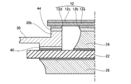
半導体装置10は、複数の外部接続端子30、32、34をさらに備える。各々の外部接続端子30、32、34は、金属(例えば銅)といった導電体で構成されており、封止体14の内外に亘って延びている。複数の外部接続端子30、32、34には、複数の信号端子30と、第1電力端子32と、第2電力端子34とが含まれる。信号端子30は、半導体素子12の信号電極12dに、はんだ層44を介して接合されている。即ち、信号端子30は、半導体素子12の信号電極12dと電気的に接続されている。なお、信号端子30と信号電極12dとの間は、はんだ層44に限られず、導電性を有する他の種類の接合層を介して接合されてもよい。
The
第1電力端子32は、図示されない位置で、絶縁回路基板20の第1導体膜24に接合されている。これにより、第1電力端子32は、第1導体膜24を介して、半導体素子12の第1主電極12bと電気的に接続されている。第2電力端子34は、半導体素子12の第2主電極12cに、はんだ層46を介して接合されている。これにより、第2電力端子34は、半導体素子12の第2主電極12cと電気的に接続されている。
The
図1、図4に示すように、信号端子30は、第1導体膜24から離れた位置で、絶縁基板22の一方の表面22aに、接合層40を介して接合されている。一例ではあるが、接合層40は、はんだ層である。また、接合層40と絶縁基板22との間には、ろう材25が設けられている。ろう材25の厚みは、接合層40の厚みよりも十分に小さい。なお、接合層40は、はんだに限定されず、他の材料で構成されてもよい。接合層40を構成する材料は、導電性の材料であってもよいし、絶縁性の材料であってもよい。ここで、ろう材25は、接合層40とともに、信号端子30と絶縁基板22との間に位置する接合層と解釈することもできる。即ち、信号端子30と絶縁基板22との間に位置する接合層(25、40)は、異なる材料で構成された多層構造を有してもよい。
As shown in FIGS. 1 and 4 , the
以上のように、本実施例の半導体装置10では、絶縁基板22上に、第1導体膜24と信号端子30とが配置されている。第1導体膜24と信号端子30との間には、一定の間隔D2が設けられており、それらの間の絶縁性が確保されている。この点に関して、詳しくは後述するが、第1導体膜24はエッチングによって形成される。そのため、第1導体膜24の周縁に沿って延びる側面24aは、裾広がりの形状を有しており、その形状を正確に管理することも困難である。従って、そのような側面24aの形状も考慮すると、第1導体膜24と信号端子30との間には、設計上、実際の間隔D2よりも大きな間隔D1を設けることが必要となる。そして、仮に二つの導体膜が隣接する場合は、それぞれの導体膜について側面の形状を考慮する必要があり、二つの導体膜の間に必要とされる設計上の間隔は、さらに大きくなってしまう。
As described above, in the
この点に関して、本実施例の半導体装置10では、絶縁基板22上の第1導体膜24に隣接して、他の導体膜ではなく、信号端子30が配置されている。そして、信号端子30は、絶縁基板22上の導体膜を介することなく、半導体素子12の信号電極12dへ電気的に接続されている。信号端子30は、絶縁基板22上に接合層40を介して接合される部材であり、例えばプレス加工といった機械加工によって製造することで、その形状を正確に管理することができる。即ち、信号端子30の側面30aが絶縁基板22と成す角度θ2は、例えば正確に90度とすることもでき、第1導体膜24の側面24aが絶縁基板22と成す角度θ1よりも、大きくすることができる。従って、第1導体膜24がエッチングによって形成される場合でも、信号端子30と第1導体膜24との間に必要とされる設計上の間隔D1は、比較的に小さくて足りる。これにより、第1導体膜24を比較的に厚く形成する場合でも、半導体装置10の大型化を避けることができる。
Regarding this point, in the
本実施例の半導体装置10では、半導体素子12の一部が、信号端子30上に位置している。そして、半導体素子12の信号電極12dは、信号端子30にはんだ層44を介して接合されている。なお、信号電極12dと信号端子30との間は、はんだ層44に限られず、導電性を有する他の種類の接合層を介して接合されてもよい。このような構成によると、信号端子30が第1導体膜24に近接して配置されるので、半導体装置10の小型化を効果的に図ることができる。
In the
本実施例の半導体装置10では、第1導体膜24の厚みが、信号端子30の厚みよりも大きくなっている。第1導体膜24の厚みが大きくなるほど、第1導体膜24の熱容量が増大することによって、半導体素子12の温度上昇を抑制することができる。特に、第1導体膜24は、半導体素子12の第1主電極12bに接合されており、半導体素子12から多くの熱を受け取ることができる。従って、信号端子30の厚みを大きくするよりも、第1導体膜24の厚みを大きくすることで、半導体素子12の温度上昇を効果的に抑制することができる。
In the
次に、図5-図10を参照して、半導体装置10の製造方法について説明する。先ず、図5に示すように、絶縁基板22を用意し、絶縁基板22の両面22a、22bにろう材25、27を塗布する。前述したように、ろう材25、27は、活性金属ろう材であってよい。次いで、図6に示すように、絶縁基板22の両面22a、22bに、導体板24x、26xを接合する。この工程では、例えば摂氏800度~1000度の雰囲気下で、絶縁基板22の両面22a、22bに配置した導体板24x、26xを、絶縁基板22に向けて押圧する。
Next, a method for manufacturing the
次いで、図7に示すように、導体板24x、26xの表面に、第1導体膜24及び第2導体膜26の形状に合わせて、レジスト膜29を形成する。次いで、図8に示すように、薬液を用いたウェットエッチングにより、導体板24x、26xを部分的に除去する。これにより、第1導体膜24及び第2導体膜26を形成するとともに、絶縁基板22上に設けられたろう材25の一部を露出させる。その後、レジスト膜29を除去する。
Next, as shown in FIG. 7, a resist
次いで、図9に示すように、絶縁基板22上に露出するろう材25上に、接合層40を介して信号端子30を接合する。信号端子30は、プレス加工といった機械加工によって、予め意図された形状(即ち、製品形状)に加工されている。信号端子30は、第1導体膜24との絶縁性を確保するために、第1導体膜24から離れた位置に接合される。特に限定されないが、接合層40ははんだ層であってよく、このときのリフロー温度は、例えば摂氏300度とすることができる。
Next, as shown in FIG. 9, the
次いで、図10に示すように、第1導体膜24及び信号端子30上に、半導体素子12を実装する。この工程では、先ず、第1導体膜24上へ半導体素子12を配置する。このとき、半導体素子12の第1主電極12bを、第1導体膜24に対向させるとともに、第1主電極12bと第1導体膜24との間にはんだシート42xを配置する。加えて、半導体素子12の一部は信号端子30上に配置し、半導体素子12の信号電極12dを信号端子30に対向させるとともに、信号電極12dと信号端子30との間にはんだシート44xを配置する。次いで、リフロー工程を実施して、はんだシート42x、44xを溶融及び再凝固させる。これにより、半導体素子12の第1主電極12bを第1導体膜24に接合するとともに、半導体素子12の信号電極12dを信号端子30に接合する。その後、電力端子32、34の組み付けや、封止体14の成形といった他の工程を実施することによって、半導体装置10は完成する。なお、本実施例の製造方法では、半導体素子12の第1主電極12bを第1導体膜24に接合する工程と、半導体素子12の信号電極12dを信号端子30に接合する工程とが、単一のリフロー工程によって並行して実施されるが、それら二つの接合する工程は別々に実施されてもよい。
Next, as shown in FIG. 10, the
本実施例の半導体装置10では、半導体素子12の信号電極12dが、はんだ層44を介して信号端子30に接合されている。これに対して、図11に示すように、信号電極12dと信号端子30との間は、ボンディングワイヤ50を介して接続されてもよい。ここで、図11に示す構成では、図1と比較して半導体素子12の向きが反転されており、第2主電極12cがはんだ層42を介して第1導体膜24に接合されている。このように、第1導体膜24には、半導体素子12の二つの主電極12b、12cのうち、どちらが接合されてもよい。
In the
図12に、一変形例の半導体装置110を示す。この半導体装置110は、上述した半導体装置10と比較して、第2絶縁回路基板120をさらに備える。第2絶縁回路基板122は、第2絶縁回路基板120は、絶縁体で構成された第2絶縁基板122と、第2絶縁基板122の一方の表面122aに設けられた第3導体膜124と、第2絶縁基板122の他方の表面122bに設けられた第4導体膜126とを備える。第3導体膜124と第4導体膜126は、それぞれろう材125、127を介して第2絶縁基板122に接合されている。そして、第3導体膜124は、はんだ層142を介して、半導体素子12の第2主電極12cに接合されている。また、図示省略するが、第2電力端子34は第3導体膜124に電気的に接続されており、第4導体膜126は封止体14の表面に露出している。
FIG. 12 shows a
図13に示すように、上述した半導体装置10、110において、信号端子30は、接合層40に接する第1区間S1と、第1区間S1から絶縁基板22の外部へ延びるとともに、第1区間S1よりも厚みの小さい第2区間S2とを有してもよい。このような構成によると、信号端子30が、絶縁基板22の周縁22eにおいて絶縁基板22と接触することがない。これにより、信号端子30と、絶縁基板22の反対側に設けられた第2導体膜26との間で、絶縁基板22に沿った沿面距離Lを長くすることができる。
As shown in FIG. 13, in the above-described
図14に示すように、上述した半導体装置10、110において、信号端子30は、半導体素子12の信号電極12dと対向する部分30bが、信号電極12dに向けて突出していてもよい。このような構成によると、信号端子30と信号電極12dとの間の距離を適切に調整することができ、例えばスペーサといった別の部材を必要とすることなく、信号端子30と信号電極12dとの間を正しく接合することができる。また、はんだ層44の過剰な濡れ広がりを抑制することができ、例えば信号電極12dと第1主電極12bとの間の意図しない短絡を避けることができる。
As shown in FIG. 14, in the
図15に他の変形例の半導体装置210を示す。この半導体装置210は、前述した変形例の半導体装置110と比較して、絶縁回路基板20の第1導体膜224の構成が変更されている。詳しくは、第1導体膜224の側面224aが、裾広がりの形状を有しておらず、絶縁基板22と略90度の角度を成している。これは、第1導体膜224がエッチングによって形成されておらず、第1導体膜224と同じプロファイルを有する導体板を機械加工で製造し、それを絶縁基板22へ接合することによって第1導体膜224が形成されているためである。このような構成によると、第1導体膜224と信号端子30との間隔をさらに縮小して、半導体装置210の小型化を図ることができる。
FIG. 15 shows a
上述した半導体装置10、110、210の構成は、様々に変更することができる。例えば、半導体装置10、110、210は、単一の半導体素子12に限られず、複数の半導体素子12を有してもよい。また、本明細書では、本技術に係る外部接続端子の構造を、信号端子30に採用した例を説明したが、同様の構造は電力端子32、34といった他の端子にも同様に採用することができる。
The configurations of the
以上、いくつかの具体例を詳細に説明したが、これらは例示に過ぎず、特許請求の範囲を限定するものではない。特許請求の範囲に記載の技術には、以上に例示した具体例を様々に変形、変更したものが含まれる。本明細書又は図面に説明した技術要素は、単独であるいは各種の組合せによって技術的有用性を発揮するものである。 Although several specific examples have been described in detail above, these are merely examples and do not limit the scope of the claims. The technology described in the claims includes various modifications and changes of the specific examples illustrated above. The technical elements described in this specification or drawings exhibit technical usefulness alone or in various combinations.
10、110、210:半導体装置
12:半導体素子
14:封止体
20、120:絶縁回路基板
22、122:絶縁基板
24、26、124、126、224:導体膜
25、27、125、127:ろう材
30:信号端子
32:第1電力端子
34:第2電力端子
40:接合層
10, 110, 210: semiconductor device 12: semiconductor element 14: sealing
Claims (12)
前記基板上の一部に設けられた第1導体膜と、
前記第1導体膜上に配置された半導体素子と、
前記第1導体膜から離れた位置で、前記基板上に接合層を介して接合された外部接続端子と、
を備え、
前記半導体素子は、主電極と信号電極とを有するパワー半導体素子であり、
前記主電極は、前記第1導体膜と電気的に接続されており、前記信号電極は、前記外部接続端子と電気的に接続されており、
前記第1導体膜の厚みは、前記外部接続端子の厚みよりも大きい、
半導体装置。 a substrate made of an insulator;
a first conductor film provided on a portion of the substrate;
a semiconductor element disposed on the first conductor film;
an external connection terminal bonded to the substrate via a bonding layer at a position away from the first conductor film;
with
The semiconductor element is a power semiconductor element having a main electrode and a signal electrode,
the main electrode is electrically connected to the first conductor film, the signal electrode is electrically connected to the external connection terminal,
the thickness of the first conductor film is greater than the thickness of the external connection terminal;
semiconductor device.
前記基板上の一部に設けられた第1導体膜と、
前記第1導体膜上に配置された半導体素子と、
前記第1導体膜から離れた位置で、前記基板上に接合層を介して接合された外部接続端子と、
を備え、
前記半導体素子は、主電極と信号電極とを有するパワー半導体素子であり、
前記主電極は、前記第1導体膜と電気的に接続されており、前記信号電極は、前記外部接続端子と電気的に接続されており、
前記外部接続端子は、前記接合層に接する第1区間と、前記第1区間から前記基板の外部へ延びるとともに、前記第1区間よりも厚みの小さい第2区間とを有する、
半導体装置。 a substrate made of an insulator;
a first conductor film provided on a portion of the substrate;
a semiconductor element disposed on the first conductor film;
an external connection terminal bonded to the substrate via a bonding layer at a position away from the first conductor film;
with
The semiconductor element is a power semiconductor element having a main electrode and a signal electrode,
the main electrode is electrically connected to the first conductor film, the signal electrode is electrically connected to the external connection terminal,
The external connection terminal has a first section in contact with the bonding layer, and a second section extending from the first section to the outside of the substrate and having a thickness smaller than that of the first section.
semiconductor device.
前記主電極は、前記IGBT構造のエミッタ又はコレクタに接続されており、
前記信号電極は、前記IGBT構造のゲートに接続されている、請求項1から6のいずれか一項に記載の半導体装置。 The semiconductor element is a power semiconductor element including an IGBT (Insulated Gate Bipolar Transistor) structure,
the main electrode is connected to the emitter or collector of the IGBT structure;
7. The semiconductor device according to claim 1, wherein said signal electrode is connected to a gate of said IGBT structure.
前記主電極は、前記MOSFETのソース又はドレインに接続されており、
前記信号電極は、前記MOSFETのゲートに接続されている、請求項1から6のいずれか一項に記載の半導体装置。 The semiconductor device is a power semiconductor device including a MOSFET (Metal-Oxide-Semiconductor Field-Effect Transistor) structure,
the main electrode is connected to the source or drain of the MOSFET,
7. The semiconductor device according to claim 1, wherein said signal electrode is connected to the gate of said MOSFET.
絶縁体で構成された基板上の導体膜を部分的にエッチングして、前記基板上の一部を覆う第1導体膜を形成する工程と、
前記第1導体膜から離れた位置で、前記基板上に接合層を介して外部接続端子を接合する工程と、
前記第1導体膜上に、主電極と信号電極とを有するパワー半導体素子を、前記主電極が前記第1導体膜に対向するように配置する工程と、
前記パワー半導体素子の前記主電極を、前記第1導体膜に接合する工程と、
前記パワー半導体素子の前記信号電極を、前記基板上に接合された前記外部接続端子へ電気的に接続する工程と、
を備え、
前記配置する工程では、前記信号電極が前記外部接続端子に対向するように、前記パワー半導体素子の一部を前記外部接続端子上に配置し、
前記電気的に接続する工程では、前記接合する工程と並行して、前記信号電極を前記外部接続端子へ接合する、
製造方法。 A method for manufacturing a semiconductor device,
partially etching a conductor film on a substrate made of an insulator to form a first conductor film covering a portion of the substrate;
bonding an external connection terminal to the substrate via a bonding layer at a position spaced apart from the first conductor film;
arranging a power semiconductor element having a main electrode and a signal electrode on the first conductor film such that the main electrode faces the first conductor film;
bonding the main electrode of the power semiconductor element to the first conductor film;
electrically connecting the signal electrode of the power semiconductor element to the external connection terminal joined on the substrate;
with
In the arranging step, a part of the power semiconductor element is arranged on the external connection terminal such that the signal electrode faces the external connection terminal;
In the electrically connecting step, the signal electrode is joined to the external connection terminal in parallel with the joining step.
Production method.
Priority Applications (4)
| Application Number | Priority Date | Filing Date | Title |
|---|---|---|---|
| JP2018239956A JP7176397B2 (en) | 2018-12-21 | 2018-12-21 | Semiconductor device and its manufacturing method |
| US16/693,478 US11201099B2 (en) | 2018-12-21 | 2019-11-25 | Semiconductor device and method of manufacturing the same |
| CN201911319896.9A CN111354710B (en) | 2018-12-21 | 2019-12-19 | Semiconductor device and manufacturing method thereof |
| DE102019135373.4A DE102019135373B4 (en) | 2018-12-21 | 2019-12-20 | Semiconductor device and method of manufacturing the same |
Applications Claiming Priority (1)
| Application Number | Priority Date | Filing Date | Title |
|---|---|---|---|
| JP2018239956A JP7176397B2 (en) | 2018-12-21 | 2018-12-21 | Semiconductor device and its manufacturing method |
Publications (2)
| Publication Number | Publication Date |
|---|---|
| JP2020102544A JP2020102544A (en) | 2020-07-02 |
| JP7176397B2 true JP7176397B2 (en) | 2022-11-22 |
Family
ID=70969295
Family Applications (1)
| Application Number | Title | Priority Date | Filing Date |
|---|---|---|---|
| JP2018239956A Active JP7176397B2 (en) | 2018-12-21 | 2018-12-21 | Semiconductor device and its manufacturing method |
Country Status (4)
| Country | Link |
|---|---|
| US (1) | US11201099B2 (en) |
| JP (1) | JP7176397B2 (en) |
| CN (1) | CN111354710B (en) |
| DE (1) | DE102019135373B4 (en) |
Families Citing this family (4)
| Publication number | Priority date | Publication date | Assignee | Title |
|---|---|---|---|---|
| KR102588851B1 (en) * | 2021-04-14 | 2023-10-16 | 주식회사 아모센스 | Power module and manufacturing method thereof |
| JP7400773B2 (en) * | 2021-05-27 | 2023-12-19 | 株式会社デンソー | semiconductor equipment |
| KR102735483B1 (en) * | 2021-12-31 | 2024-11-28 | 주식회사 아모센스 | Ceramic substrate unit and manufacturing method thereof |
| JP7802187B2 (en) * | 2022-09-09 | 2026-01-19 | 三菱電機株式会社 | Semiconductor Devices |
Citations (2)
| Publication number | Priority date | Publication date | Assignee | Title |
|---|---|---|---|---|
| JP2013183022A (en) | 2012-03-01 | 2013-09-12 | Toyota Industries Corp | Semiconductor device and manufacturing apparatus of the same |
| JP2016174165A (en) | 2011-12-20 | 2016-09-29 | 株式会社東芝 | Semiconductor device |
Family Cites Families (19)
| Publication number | Priority date | Publication date | Assignee | Title |
|---|---|---|---|---|
| US4538170A (en) | 1983-01-03 | 1985-08-27 | General Electric Company | Power chip package |
| JPH05343591A (en) | 1992-06-11 | 1993-12-24 | Sumitomo Metal Ind Ltd | Lead frame and manufacture thereof |
| JP3879150B2 (en) * | 1996-08-12 | 2007-02-07 | 株式会社デンソー | Semiconductor device |
| JP2007251076A (en) | 2006-03-20 | 2007-09-27 | Hitachi Ltd | Power semiconductor module |
| DE102006034679A1 (en) * | 2006-07-24 | 2008-01-31 | Infineon Technologies Ag | Semiconductor module with power semiconductor chip and passive component and method for producing the same |
| US7557434B2 (en) | 2006-08-29 | 2009-07-07 | Denso Corporation | Power electronic package having two substrates with multiple electronic components |
| DE102006049949B3 (en) * | 2006-10-19 | 2008-05-15 | Infineon Technologies Ag | Semiconductor module, has flat conductor chip island defining electrically conducting portion and insulation layer, and semiconductor chip arranged on electrically conducting portion and positively bonded on insulation layer |
| US8164176B2 (en) * | 2006-10-20 | 2012-04-24 | Infineon Technologies Ag | Semiconductor module arrangement |
| KR101493865B1 (en) * | 2007-11-16 | 2015-02-17 | 페어차일드코리아반도체 주식회사 | Semiconductor power module package with simplified structure and manufacturing method thereof |
| JP5257817B2 (en) * | 2010-06-15 | 2013-08-07 | 三菱電機株式会社 | Semiconductor device |
| JP2012146760A (en) | 2011-01-11 | 2012-08-02 | Calsonic Kansei Corp | Power semiconductor module |
| JP5786972B2 (en) * | 2012-02-14 | 2015-09-30 | 三菱電機株式会社 | Semiconductor device |
| WO2014006724A1 (en) * | 2012-07-05 | 2014-01-09 | 三菱電機株式会社 | Semiconductor device |
| JP6152893B2 (en) * | 2013-09-30 | 2017-06-28 | 富士電機株式会社 | Semiconductor device, method for assembling semiconductor device, component for semiconductor device, and unit module |
| DE102015104996B4 (en) * | 2015-03-31 | 2020-06-18 | Infineon Technologies Austria Ag | Semiconductor devices with control and load lines from opposite directions |
| DE102015104990B4 (en) * | 2015-03-31 | 2020-06-04 | Infineon Technologies Austria Ag | Compound semiconductor device with a scanning lead |
| JP6897141B2 (en) * | 2017-02-15 | 2021-06-30 | 株式会社デンソー | Semiconductor devices and their manufacturing methods |
| JP6809294B2 (en) * | 2017-03-02 | 2021-01-06 | 三菱電機株式会社 | Power module |
| JP7260278B2 (en) * | 2018-10-19 | 2023-04-18 | 現代自動車株式会社 | Semiconductor subassemblies and semiconductor power modules |
-
2018
- 2018-12-21 JP JP2018239956A patent/JP7176397B2/en active Active
-
2019
- 2019-11-25 US US16/693,478 patent/US11201099B2/en active Active
- 2019-12-19 CN CN201911319896.9A patent/CN111354710B/en active Active
- 2019-12-20 DE DE102019135373.4A patent/DE102019135373B4/en active Active
Patent Citations (2)
| Publication number | Priority date | Publication date | Assignee | Title |
|---|---|---|---|---|
| JP2016174165A (en) | 2011-12-20 | 2016-09-29 | 株式会社東芝 | Semiconductor device |
| JP2013183022A (en) | 2012-03-01 | 2013-09-12 | Toyota Industries Corp | Semiconductor device and manufacturing apparatus of the same |
Also Published As
| Publication number | Publication date |
|---|---|
| JP2020102544A (en) | 2020-07-02 |
| DE102019135373A1 (en) | 2020-06-25 |
| US20200203252A1 (en) | 2020-06-25 |
| CN111354710A (en) | 2020-06-30 |
| US11201099B2 (en) | 2021-12-14 |
| CN111354710B (en) | 2023-08-04 |
| DE102019135373B4 (en) | 2024-07-11 |
Similar Documents
| Publication | Publication Date | Title |
|---|---|---|
| US7456492B2 (en) | Semiconductor device having semiconductor element, insulation substrate and metal electrode | |
| JP7176397B2 (en) | Semiconductor device and its manufacturing method | |
| JP4885046B2 (en) | Power semiconductor module | |
| JP2007073743A (en) | Semiconductor device | |
| US10903138B2 (en) | Semiconductor device and method of manufacturing the same | |
| CN113039636A (en) | Power semiconductor device | |
| CN111276447A (en) | Double-side cooling power module and manufacturing method thereof | |
| CN102437138A (en) | Semiconductor device | |
| JP7124474B2 (en) | semiconductor equipment | |
| WO2023149144A1 (en) | Semiconductor device | |
| CN115206919A (en) | Semiconductor device with a plurality of semiconductor chips | |
| JP5217015B2 (en) | Power converter and manufacturing method thereof | |
| JP2019083294A (en) | Semiconductor device and method for manufacturing the same | |
| JP7163583B2 (en) | semiconductor equipment | |
| JP2006190728A (en) | Power semiconductor device | |
| JP2017054855A (en) | Semiconductor device and semiconductor package | |
| JP2019083292A (en) | Semiconductor device | |
| US12581969B2 (en) | Semiconductor device | |
| CN115206905B (en) | Semiconductor device and semiconductor module using the same | |
| CN111599781A (en) | Semiconductor device with a plurality of semiconductor chips | |
| JP2021034701A (en) | Semiconductor device | |
| JP7180533B2 (en) | semiconductor equipment | |
| WO2024024067A1 (en) | Electric power conversion device, and method for producing electric power conversion device | |
| JP2021111719A (en) | Semiconductor device | |
| JP2014033125A (en) | Semiconductor device and manufacturing method of the same |
Legal Events
| Date | Code | Title | Description |
|---|---|---|---|
| A711 | Notification of change in applicant |
Free format text: JAPANESE INTERMEDIATE CODE: A711 Effective date: 20200401 |
|
| A621 | Written request for application examination |
Free format text: JAPANESE INTERMEDIATE CODE: A621 Effective date: 20210520 |
|
| A977 | Report on retrieval |
Free format text: JAPANESE INTERMEDIATE CODE: A971007 Effective date: 20220330 |
|
| A131 | Notification of reasons for refusal |
Free format text: JAPANESE INTERMEDIATE CODE: A131 Effective date: 20220412 |
|
| A521 | Request for written amendment filed |
Free format text: JAPANESE INTERMEDIATE CODE: A523 Effective date: 20220603 |
|
| TRDD | Decision of grant or rejection written | ||
| A01 | Written decision to grant a patent or to grant a registration (utility model) |
Free format text: JAPANESE INTERMEDIATE CODE: A01 Effective date: 20221011 |
|
| A61 | First payment of annual fees (during grant procedure) |
Free format text: JAPANESE INTERMEDIATE CODE: A61 Effective date: 20221024 |
|
| R151 | Written notification of patent or utility model registration |
Ref document number: 7176397 Country of ref document: JP Free format text: JAPANESE INTERMEDIATE CODE: R151 |
|
| R250 | Receipt of annual fees |
Free format text: JAPANESE INTERMEDIATE CODE: R250 |