JP6987520B2 - 半導体装置 - Google Patents
半導体装置 Download PDFInfo
- Publication number
- JP6987520B2 JP6987520B2 JP2017074988A JP2017074988A JP6987520B2 JP 6987520 B2 JP6987520 B2 JP 6987520B2 JP 2017074988 A JP2017074988 A JP 2017074988A JP 2017074988 A JP2017074988 A JP 2017074988A JP 6987520 B2 JP6987520 B2 JP 6987520B2
- Authority
- JP
- Japan
- Prior art keywords
- insulating layer
- layer
- oxide semiconductor
- transistor
- oxide
- Prior art date
- Legal status (The legal status is an assumption and is not a legal conclusion. Google has not performed a legal analysis and makes no representation as to the accuracy of the status listed.)
- Active
Links
- 239000004065 semiconductor Substances 0.000 title claims description 523
- 229910052581 Si3N4 Inorganic materials 0.000 claims description 54
- HQVNEWCFYHHQES-UHFFFAOYSA-N silicon nitride Chemical compound N12[Si]34N5[Si]62N3[Si]51N64 HQVNEWCFYHHQES-UHFFFAOYSA-N 0.000 claims description 54
- 239000010949 copper Substances 0.000 claims description 34
- TWNQGVIAIRXVLR-UHFFFAOYSA-N oxo(oxoalumanyloxy)alumane Chemical compound O=[Al]O[Al]=O TWNQGVIAIRXVLR-UHFFFAOYSA-N 0.000 claims description 33
- RYGMFSIKBFXOCR-UHFFFAOYSA-N Copper Chemical group [Cu] RYGMFSIKBFXOCR-UHFFFAOYSA-N 0.000 claims description 32
- 229910052802 copper Inorganic materials 0.000 claims description 32
- PMHQVHHXPFUNSP-UHFFFAOYSA-M copper(1+);methylsulfanylmethane;bromide Chemical compound Br[Cu].CSC PMHQVHHXPFUNSP-UHFFFAOYSA-M 0.000 claims description 18
- AJNVQOSZGJRYEI-UHFFFAOYSA-N digallium;oxygen(2-) Chemical compound [O-2].[O-2].[O-2].[Ga+3].[Ga+3] AJNVQOSZGJRYEI-UHFFFAOYSA-N 0.000 claims description 8
- 229910001195 gallium oxide Inorganic materials 0.000 claims description 8
- MRELNEQAGSRDBK-UHFFFAOYSA-N lanthanum(3+);oxygen(2-) Chemical compound [O-2].[O-2].[O-2].[La+3].[La+3] MRELNEQAGSRDBK-UHFFFAOYSA-N 0.000 claims description 8
- PLDDOISOJJCEMH-UHFFFAOYSA-N neodymium(3+);oxygen(2-) Chemical compound [O-2].[O-2].[O-2].[Nd+3].[Nd+3] PLDDOISOJJCEMH-UHFFFAOYSA-N 0.000 claims description 8
- YBMRDBCBODYGJE-UHFFFAOYSA-N germanium oxide Inorganic materials O=[Ge]=O YBMRDBCBODYGJE-UHFFFAOYSA-N 0.000 claims description 4
- 229910000449 hafnium oxide Inorganic materials 0.000 claims description 4
- WIHZLLGSGQNAGK-UHFFFAOYSA-N hafnium(4+);oxygen(2-) Chemical compound [O-2].[O-2].[Hf+4] WIHZLLGSGQNAGK-UHFFFAOYSA-N 0.000 claims description 4
- SIWVEOZUMHYXCS-UHFFFAOYSA-N oxo(oxoyttriooxy)yttrium Chemical compound O=[Y]O[Y]=O SIWVEOZUMHYXCS-UHFFFAOYSA-N 0.000 claims description 4
- PVADDRMAFCOOPC-UHFFFAOYSA-N oxogermanium Chemical compound [Ge]=O PVADDRMAFCOOPC-UHFFFAOYSA-N 0.000 claims description 4
- BPUBBGLMJRNUCC-UHFFFAOYSA-N oxygen(2-);tantalum(5+) Chemical compound [O-2].[O-2].[O-2].[O-2].[O-2].[Ta+5].[Ta+5] BPUBBGLMJRNUCC-UHFFFAOYSA-N 0.000 claims description 4
- RVTZCBVAJQQJTK-UHFFFAOYSA-N oxygen(2-);zirconium(4+) Chemical compound [O-2].[O-2].[Zr+4] RVTZCBVAJQQJTK-UHFFFAOYSA-N 0.000 claims description 4
- 229910001936 tantalum oxide Inorganic materials 0.000 claims description 4
- 229910001928 zirconium oxide Inorganic materials 0.000 claims description 4
- 239000010410 layer Substances 0.000 description 1102
- 238000000034 method Methods 0.000 description 174
- 229910052760 oxygen Inorganic materials 0.000 description 170
- 239000001301 oxygen Substances 0.000 description 170
- QVGXLLKOCUKJST-UHFFFAOYSA-N atomic oxygen Chemical compound [O] QVGXLLKOCUKJST-UHFFFAOYSA-N 0.000 description 166
- 239000007789 gas Substances 0.000 description 132
- 239000010408 film Substances 0.000 description 102
- 239000000758 substrate Substances 0.000 description 95
- 238000010438 heat treatment Methods 0.000 description 83
- IJGRMHOSHXDMSA-UHFFFAOYSA-N Atomic nitrogen Chemical compound N#N IJGRMHOSHXDMSA-UHFFFAOYSA-N 0.000 description 81
- 230000006870 function Effects 0.000 description 80
- 238000004544 sputter deposition Methods 0.000 description 72
- 239000011701 zinc Substances 0.000 description 69
- 229910052739 hydrogen Inorganic materials 0.000 description 61
- 239000001257 hydrogen Substances 0.000 description 61
- 239000012535 impurity Substances 0.000 description 55
- 229910052738 indium Inorganic materials 0.000 description 48
- 230000002829 reductive effect Effects 0.000 description 47
- 239000012298 atmosphere Substances 0.000 description 46
- 239000004973 liquid crystal related substance Substances 0.000 description 46
- 239000000463 material Substances 0.000 description 44
- UFHFLCQGNIYNRP-UHFFFAOYSA-N Hydrogen Chemical compound [H][H] UFHFLCQGNIYNRP-UHFFFAOYSA-N 0.000 description 41
- APFVFJFRJDLVQX-UHFFFAOYSA-N indium atom Chemical compound [In] APFVFJFRJDLVQX-UHFFFAOYSA-N 0.000 description 39
- 229910052757 nitrogen Inorganic materials 0.000 description 38
- XUIMIQQOPSSXEZ-UHFFFAOYSA-N Silicon Chemical compound [Si] XUIMIQQOPSSXEZ-UHFFFAOYSA-N 0.000 description 35
- 229910052710 silicon Inorganic materials 0.000 description 35
- 239000010703 silicon Substances 0.000 description 35
- 239000013078 crystal Substances 0.000 description 34
- 239000000203 mixture Substances 0.000 description 32
- XLOMVQKBTHCTTD-UHFFFAOYSA-N Zinc monoxide Chemical compound [Zn]=O XLOMVQKBTHCTTD-UHFFFAOYSA-N 0.000 description 31
- MWUXSHHQAYIFBG-UHFFFAOYSA-N nitrogen oxide Inorganic materials O=[N] MWUXSHHQAYIFBG-UHFFFAOYSA-N 0.000 description 31
- 238000004519 manufacturing process Methods 0.000 description 29
- 239000004020 conductor Substances 0.000 description 28
- 238000011282 treatment Methods 0.000 description 28
- 125000004429 atom Chemical group 0.000 description 27
- -1 for example Substances 0.000 description 25
- 239000002994 raw material Substances 0.000 description 23
- XLYOFNOQVPJJNP-UHFFFAOYSA-N water Substances O XLYOFNOQVPJJNP-UHFFFAOYSA-N 0.000 description 23
- XKRFYHLGVUSROY-UHFFFAOYSA-N Argon Chemical compound [Ar] XKRFYHLGVUSROY-UHFFFAOYSA-N 0.000 description 22
- 230000000694 effects Effects 0.000 description 22
- 230000001590 oxidative effect Effects 0.000 description 22
- 230000007547 defect Effects 0.000 description 21
- 230000008569 process Effects 0.000 description 21
- OKTJSMMVPCPJKN-UHFFFAOYSA-N Carbon Chemical compound [C] OKTJSMMVPCPJKN-UHFFFAOYSA-N 0.000 description 20
- GQPLMRYTRLFLPF-UHFFFAOYSA-N Nitrous Oxide Chemical compound [O-][N+]#N GQPLMRYTRLFLPF-UHFFFAOYSA-N 0.000 description 20
- 238000000231 atomic layer deposition Methods 0.000 description 20
- 230000015572 biosynthetic process Effects 0.000 description 20
- 150000002431 hydrogen Chemical class 0.000 description 20
- 238000012545 processing Methods 0.000 description 20
- 229910052814 silicon oxide Inorganic materials 0.000 description 20
- 238000001312 dry etching Methods 0.000 description 19
- 229910052733 gallium Inorganic materials 0.000 description 19
- 239000011810 insulating material Substances 0.000 description 19
- 230000037230 mobility Effects 0.000 description 19
- 238000001039 wet etching Methods 0.000 description 19
- GYHNNYVSQQEPJS-UHFFFAOYSA-N Gallium Chemical compound [Ga] GYHNNYVSQQEPJS-UHFFFAOYSA-N 0.000 description 17
- 238000006243 chemical reaction Methods 0.000 description 17
- 238000000623 plasma-assisted chemical vapour deposition Methods 0.000 description 17
- 239000011787 zinc oxide Substances 0.000 description 17
- 239000010936 titanium Substances 0.000 description 16
- PXHVJJICTQNCMI-UHFFFAOYSA-N Nickel Chemical compound [Ni] PXHVJJICTQNCMI-UHFFFAOYSA-N 0.000 description 15
- 230000005684 electric field Effects 0.000 description 15
- 229910052751 metal Inorganic materials 0.000 description 15
- 229920005989 resin Polymers 0.000 description 15
- 239000011347 resin Substances 0.000 description 15
- QGZKDVFQNNGYKY-UHFFFAOYSA-N Ammonia Chemical compound N QGZKDVFQNNGYKY-UHFFFAOYSA-N 0.000 description 14
- 238000005530 etching Methods 0.000 description 14
- 239000002184 metal Substances 0.000 description 14
- BLRPTPMANUNPDV-UHFFFAOYSA-N Silane Chemical compound [SiH4] BLRPTPMANUNPDV-UHFFFAOYSA-N 0.000 description 13
- RTAQQCXQSZGOHL-UHFFFAOYSA-N Titanium Chemical compound [Ti] RTAQQCXQSZGOHL-UHFFFAOYSA-N 0.000 description 13
- 229910052782 aluminium Inorganic materials 0.000 description 13
- XAGFODPZIPBFFR-UHFFFAOYSA-N aluminium Chemical compound [Al] XAGFODPZIPBFFR-UHFFFAOYSA-N 0.000 description 13
- 238000009792 diffusion process Methods 0.000 description 13
- 230000004048 modification Effects 0.000 description 13
- 238000012986 modification Methods 0.000 description 13
- 229910000077 silane Inorganic materials 0.000 description 13
- 229910052719 titanium Inorganic materials 0.000 description 13
- HCHKCACWOHOZIP-UHFFFAOYSA-N Zinc Chemical compound [Zn] HCHKCACWOHOZIP-UHFFFAOYSA-N 0.000 description 12
- 239000012466 permeate Substances 0.000 description 12
- 238000000206 photolithography Methods 0.000 description 12
- 229910052725 zinc Inorganic materials 0.000 description 12
- 229910052786 argon Inorganic materials 0.000 description 11
- 239000000126 substance Substances 0.000 description 11
- 230000005669 field effect Effects 0.000 description 10
- 239000011521 glass Substances 0.000 description 10
- 206010021143 Hypoxia Diseases 0.000 description 9
- 229910052799 carbon Inorganic materials 0.000 description 9
- 230000006378 damage Effects 0.000 description 9
- XEEYBQQBJWHFJM-UHFFFAOYSA-N iron Substances [Fe] XEEYBQQBJWHFJM-UHFFFAOYSA-N 0.000 description 9
- 150000004767 nitrides Chemical class 0.000 description 9
- 239000001272 nitrous oxide Substances 0.000 description 9
- YVTHLONGBIQYBO-UHFFFAOYSA-N zinc indium(3+) oxygen(2-) Chemical compound [O--].[Zn++].[In+3] YVTHLONGBIQYBO-UHFFFAOYSA-N 0.000 description 9
- 230000007423 decrease Effects 0.000 description 8
- AMGQUBHHOARCQH-UHFFFAOYSA-N indium;oxotin Chemical compound [In].[Sn]=O AMGQUBHHOARCQH-UHFFFAOYSA-N 0.000 description 8
- 239000011261 inert gas Substances 0.000 description 8
- 238000009413 insulation Methods 0.000 description 8
- 238000005468 ion implantation Methods 0.000 description 8
- 238000009832 plasma treatment Methods 0.000 description 8
- 238000007639 printing Methods 0.000 description 8
- 239000003566 sealing material Substances 0.000 description 8
- 238000012360 testing method Methods 0.000 description 8
- 229910002601 GaN Inorganic materials 0.000 description 7
- 229910052784 alkaline earth metal Inorganic materials 0.000 description 7
- 239000000969 carrier Substances 0.000 description 7
- 238000005229 chemical vapour deposition Methods 0.000 description 7
- 238000004891 communication Methods 0.000 description 7
- 230000008595 infiltration Effects 0.000 description 7
- 238000001764 infiltration Methods 0.000 description 7
- 229910052759 nickel Inorganic materials 0.000 description 7
- VYPSYNLAJGMNEJ-UHFFFAOYSA-N silicon dioxide Inorganic materials O=[Si]=O VYPSYNLAJGMNEJ-UHFFFAOYSA-N 0.000 description 7
- 229910045601 alloy Inorganic materials 0.000 description 6
- 239000000956 alloy Substances 0.000 description 6
- 230000008859 change Effects 0.000 description 6
- 238000004140 cleaning Methods 0.000 description 6
- 150000001875 compounds Chemical class 0.000 description 6
- 229910021389 graphene Inorganic materials 0.000 description 6
- 238000005259 measurement Methods 0.000 description 6
- 229910052756 noble gas Inorganic materials 0.000 description 6
- BASFCYQUMIYNBI-UHFFFAOYSA-N platinum Chemical compound [Pt] BASFCYQUMIYNBI-UHFFFAOYSA-N 0.000 description 6
- 238000001004 secondary ion mass spectrometry Methods 0.000 description 6
- 239000002356 single layer Substances 0.000 description 6
- 238000003860 storage Methods 0.000 description 6
- 229910052783 alkali metal Inorganic materials 0.000 description 5
- 150000001340 alkali metals Chemical class 0.000 description 5
- 150000001342 alkaline earth metals Chemical class 0.000 description 5
- 229910021529 ammonia Inorganic materials 0.000 description 5
- 239000011651 chromium Substances 0.000 description 5
- 229910052742 iron Inorganic materials 0.000 description 5
- 239000007788 liquid Substances 0.000 description 5
- 239000011159 matrix material Substances 0.000 description 5
- 229910052750 molybdenum Inorganic materials 0.000 description 5
- 230000003287 optical effect Effects 0.000 description 5
- 239000002245 particle Substances 0.000 description 5
- 229910052715 tantalum Inorganic materials 0.000 description 5
- GUVRBAGPIYLISA-UHFFFAOYSA-N tantalum atom Chemical compound [Ta] GUVRBAGPIYLISA-UHFFFAOYSA-N 0.000 description 5
- WFKWXMTUELFFGS-UHFFFAOYSA-N tungsten Chemical compound [W] WFKWXMTUELFFGS-UHFFFAOYSA-N 0.000 description 5
- 229910052721 tungsten Inorganic materials 0.000 description 5
- 239000010937 tungsten Substances 0.000 description 5
- CURLTUGMZLYLDI-UHFFFAOYSA-N Carbon dioxide Chemical compound O=C=O CURLTUGMZLYLDI-UHFFFAOYSA-N 0.000 description 4
- MYMOFIZGZYHOMD-UHFFFAOYSA-N Dioxygen Chemical compound O=O MYMOFIZGZYHOMD-UHFFFAOYSA-N 0.000 description 4
- ZOKXTWBITQBERF-UHFFFAOYSA-N Molybdenum Chemical compound [Mo] ZOKXTWBITQBERF-UHFFFAOYSA-N 0.000 description 4
- CBENFWSGALASAD-UHFFFAOYSA-N Ozone Chemical compound [O-][O+]=O CBENFWSGALASAD-UHFFFAOYSA-N 0.000 description 4
- OAICVXFJPJFONN-UHFFFAOYSA-N Phosphorus Chemical compound [P] OAICVXFJPJFONN-UHFFFAOYSA-N 0.000 description 4
- GWEVSGVZZGPLCZ-UHFFFAOYSA-N Titan oxide Chemical compound O=[Ti]=O GWEVSGVZZGPLCZ-UHFFFAOYSA-N 0.000 description 4
- 229920001940 conductive polymer Polymers 0.000 description 4
- 230000002950 deficient Effects 0.000 description 4
- 238000003795 desorption Methods 0.000 description 4
- 229910001882 dioxygen Inorganic materials 0.000 description 4
- KPUWHANPEXNPJT-UHFFFAOYSA-N disiloxane Chemical class [SiH3]O[SiH3] KPUWHANPEXNPJT-UHFFFAOYSA-N 0.000 description 4
- 238000010894 electron beam technology Methods 0.000 description 4
- 229910002804 graphite Inorganic materials 0.000 description 4
- 239000010439 graphite Substances 0.000 description 4
- 229910052735 hafnium Inorganic materials 0.000 description 4
- VBJZVLUMGGDVMO-UHFFFAOYSA-N hafnium atom Chemical compound [Hf] VBJZVLUMGGDVMO-UHFFFAOYSA-N 0.000 description 4
- 229910003437 indium oxide Inorganic materials 0.000 description 4
- PJXISJQVUVHSOJ-UHFFFAOYSA-N indium(iii) oxide Chemical compound [O-2].[O-2].[O-2].[In+3].[In+3] PJXISJQVUVHSOJ-UHFFFAOYSA-N 0.000 description 4
- 229910010272 inorganic material Inorganic materials 0.000 description 4
- 238000010884 ion-beam technique Methods 0.000 description 4
- 150000002500 ions Chemical class 0.000 description 4
- 239000011777 magnesium Substances 0.000 description 4
- 239000011733 molybdenum Substances 0.000 description 4
- 239000010955 niobium Substances 0.000 description 4
- QGLKJKCYBOYXKC-UHFFFAOYSA-N nonaoxidotritungsten Chemical compound O=[W]1(=O)O[W](=O)(=O)O[W](=O)(=O)O1 QGLKJKCYBOYXKC-UHFFFAOYSA-N 0.000 description 4
- 238000005192 partition Methods 0.000 description 4
- 229910052698 phosphorus Inorganic materials 0.000 description 4
- 239000011574 phosphorus Substances 0.000 description 4
- 239000011241 protective layer Substances 0.000 description 4
- OGIDPMRJRNCKJF-UHFFFAOYSA-N titanium oxide Inorganic materials [Ti]=O OGIDPMRJRNCKJF-UHFFFAOYSA-N 0.000 description 4
- 229910001930 tungsten oxide Inorganic materials 0.000 description 4
- ZOXJGFHDIHLPTG-UHFFFAOYSA-N Boron Chemical compound [B] ZOXJGFHDIHLPTG-UHFFFAOYSA-N 0.000 description 3
- ZAMOUSCENKQFHK-UHFFFAOYSA-N Chlorine atom Chemical compound [Cl] ZAMOUSCENKQFHK-UHFFFAOYSA-N 0.000 description 3
- FYYHWMGAXLPEAU-UHFFFAOYSA-N Magnesium Chemical compound [Mg] FYYHWMGAXLPEAU-UHFFFAOYSA-N 0.000 description 3
- 239000004642 Polyimide Substances 0.000 description 3
- BQCADISMDOOEFD-UHFFFAOYSA-N Silver Chemical compound [Ag] BQCADISMDOOEFD-UHFFFAOYSA-N 0.000 description 3
- 230000009471 action Effects 0.000 description 3
- 229910021417 amorphous silicon Inorganic materials 0.000 description 3
- 230000000903 blocking effect Effects 0.000 description 3
- 229910052796 boron Inorganic materials 0.000 description 3
- 239000005388 borosilicate glass Substances 0.000 description 3
- 239000000460 chlorine Substances 0.000 description 3
- 229910052801 chlorine Inorganic materials 0.000 description 3
- 229910052804 chromium Inorganic materials 0.000 description 3
- 230000006866 deterioration Effects 0.000 description 3
- 229910001873 dinitrogen Inorganic materials 0.000 description 3
- 230000005611 electricity Effects 0.000 description 3
- 238000005401 electroluminescence Methods 0.000 description 3
- 239000005262 ferroelectric liquid crystals (FLCs) Substances 0.000 description 3
- 239000000945 filler Substances 0.000 description 3
- 238000007654 immersion Methods 0.000 description 3
- 238000002513 implantation Methods 0.000 description 3
- 239000011147 inorganic material Substances 0.000 description 3
- 229910052749 magnesium Inorganic materials 0.000 description 3
- 239000011572 manganese Substances 0.000 description 3
- 230000007246 mechanism Effects 0.000 description 3
- 239000012299 nitrogen atmosphere Substances 0.000 description 3
- 239000011368 organic material Substances 0.000 description 3
- 229920001721 polyimide Polymers 0.000 description 3
- 239000002096 quantum dot Substances 0.000 description 3
- 229910052709 silver Inorganic materials 0.000 description 3
- 239000004332 silver Substances 0.000 description 3
- 238000001179 sorption measurement Methods 0.000 description 3
- 125000006850 spacer group Chemical group 0.000 description 3
- 230000003068 static effect Effects 0.000 description 3
- 238000002230 thermal chemical vapour deposition Methods 0.000 description 3
- 238000007740 vapor deposition Methods 0.000 description 3
- 239000011800 void material Substances 0.000 description 3
- UWCWUCKPEYNDNV-LBPRGKRZSA-N 2,6-dimethyl-n-[[(2s)-pyrrolidin-2-yl]methyl]aniline Chemical compound CC1=CC=CC(C)=C1NC[C@H]1NCCC1 UWCWUCKPEYNDNV-LBPRGKRZSA-N 0.000 description 2
- MGWGWNFMUOTEHG-UHFFFAOYSA-N 4-(3,5-dimethylphenyl)-1,3-thiazol-2-amine Chemical compound CC1=CC(C)=CC(C=2N=C(N)SC=2)=C1 MGWGWNFMUOTEHG-UHFFFAOYSA-N 0.000 description 2
- 229920000178 Acrylic resin Polymers 0.000 description 2
- 239000004925 Acrylic resin Substances 0.000 description 2
- PAYRUJLWNCNPSJ-UHFFFAOYSA-N Aniline Chemical compound NC1=CC=CC=C1 PAYRUJLWNCNPSJ-UHFFFAOYSA-N 0.000 description 2
- 229910052684 Cerium Inorganic materials 0.000 description 2
- VYZAMTAEIAYCRO-UHFFFAOYSA-N Chromium Chemical compound [Cr] VYZAMTAEIAYCRO-UHFFFAOYSA-N 0.000 description 2
- KRHYYFGTRYWZRS-UHFFFAOYSA-N Fluorane Chemical compound F KRHYYFGTRYWZRS-UHFFFAOYSA-N 0.000 description 2
- 229910052779 Neodymium Inorganic materials 0.000 description 2
- 239000004952 Polyamide Substances 0.000 description 2
- 239000004983 Polymer Dispersed Liquid Crystal Substances 0.000 description 2
- KAESVJOAVNADME-UHFFFAOYSA-N Pyrrole Chemical compound C=1C=CNC=1 KAESVJOAVNADME-UHFFFAOYSA-N 0.000 description 2
- 229910000577 Silicon-germanium Inorganic materials 0.000 description 2
- YTPLMLYBLZKORZ-UHFFFAOYSA-N Thiophene Chemical compound C=1C=CSC=1 YTPLMLYBLZKORZ-UHFFFAOYSA-N 0.000 description 2
- ATJFFYVFTNAWJD-UHFFFAOYSA-N Tin Chemical compound [Sn] ATJFFYVFTNAWJD-UHFFFAOYSA-N 0.000 description 2
- 239000007983 Tris buffer Substances 0.000 description 2
- QCWXUUIWCKQGHC-UHFFFAOYSA-N Zirconium Chemical compound [Zr] QCWXUUIWCKQGHC-UHFFFAOYSA-N 0.000 description 2
- LEVVHYCKPQWKOP-UHFFFAOYSA-N [Si].[Ge] Chemical compound [Si].[Ge] LEVVHYCKPQWKOP-UHFFFAOYSA-N 0.000 description 2
- 125000005595 acetylacetonate group Chemical group 0.000 description 2
- NIXOWILDQLNWCW-UHFFFAOYSA-N acrylic acid group Chemical group C(C=C)(=O)O NIXOWILDQLNWCW-UHFFFAOYSA-N 0.000 description 2
- 239000005354 aluminosilicate glass Substances 0.000 description 2
- 239000004760 aramid Substances 0.000 description 2
- 229920003235 aromatic polyamide Polymers 0.000 description 2
- 238000004380 ashing Methods 0.000 description 2
- 238000001505 atmospheric-pressure chemical vapour deposition Methods 0.000 description 2
- 229910052795 boron group element Inorganic materials 0.000 description 2
- 239000000872 buffer Substances 0.000 description 2
- DQXBYHZEEUGOBF-UHFFFAOYSA-N but-3-enoic acid;ethene Chemical compound C=C.OC(=O)CC=C DQXBYHZEEUGOBF-UHFFFAOYSA-N 0.000 description 2
- 239000001569 carbon dioxide Substances 0.000 description 2
- 229910002092 carbon dioxide Inorganic materials 0.000 description 2
- 229910052800 carbon group element Inorganic materials 0.000 description 2
- 239000000919 ceramic Substances 0.000 description 2
- ZMIGMASIKSOYAM-UHFFFAOYSA-N cerium Chemical compound [Ce][Ce][Ce][Ce][Ce][Ce][Ce][Ce][Ce][Ce][Ce][Ce][Ce][Ce][Ce][Ce][Ce][Ce][Ce][Ce][Ce][Ce][Ce][Ce][Ce][Ce][Ce][Ce][Ce][Ce][Ce][Ce][Ce][Ce][Ce][Ce][Ce][Ce] ZMIGMASIKSOYAM-UHFFFAOYSA-N 0.000 description 2
- 230000003098 cholesteric effect Effects 0.000 description 2
- 238000000354 decomposition reaction Methods 0.000 description 2
- 239000002274 desiccant Substances 0.000 description 2
- 238000013461 design Methods 0.000 description 2
- AXAZMDOAUQTMOW-UHFFFAOYSA-N dimethylzinc Chemical compound C[Zn]C AXAZMDOAUQTMOW-UHFFFAOYSA-N 0.000 description 2
- PZPGRFITIJYNEJ-UHFFFAOYSA-N disilane Chemical compound [SiH3][SiH3] PZPGRFITIJYNEJ-UHFFFAOYSA-N 0.000 description 2
- 230000005685 electric field effect Effects 0.000 description 2
- 239000005038 ethylene vinyl acetate Substances 0.000 description 2
- 230000005281 excited state Effects 0.000 description 2
- 125000001153 fluoro group Chemical group F* 0.000 description 2
- YRBSWAUAPBXXMZ-UHFFFAOYSA-N gallium;pentane-2,4-dione Chemical compound [Ga].CC(=O)CC(C)=O.CC(=O)CC(C)=O.CC(=O)CC(C)=O YRBSWAUAPBXXMZ-UHFFFAOYSA-N 0.000 description 2
- 238000004868 gas analysis Methods 0.000 description 2
- 229910052732 germanium Inorganic materials 0.000 description 2
- GNPVGFCGXDBREM-UHFFFAOYSA-N germanium atom Chemical compound [Ge] GNPVGFCGXDBREM-UHFFFAOYSA-N 0.000 description 2
- 239000010931 gold Substances 0.000 description 2
- 229910001385 heavy metal Inorganic materials 0.000 description 2
- 238000002347 injection Methods 0.000 description 2
- 239000007924 injection Substances 0.000 description 2
- 230000010354 integration Effects 0.000 description 2
- 230000001678 irradiating effect Effects 0.000 description 2
- 229910052746 lanthanum Inorganic materials 0.000 description 2
- FZLIPJUXYLNCLC-UHFFFAOYSA-N lanthanum atom Chemical compound [La] FZLIPJUXYLNCLC-UHFFFAOYSA-N 0.000 description 2
- 238000001307 laser spectroscopy Methods 0.000 description 2
- 238000004518 low pressure chemical vapour deposition Methods 0.000 description 2
- 229910052748 manganese Inorganic materials 0.000 description 2
- 239000012528 membrane Substances 0.000 description 2
- 238000002156 mixing Methods 0.000 description 2
- QEFYFXOXNSNQGX-UHFFFAOYSA-N neodymium atom Chemical compound [Nd] QEFYFXOXNSNQGX-UHFFFAOYSA-N 0.000 description 2
- 229910052758 niobium Inorganic materials 0.000 description 2
- GUCVJGMIXFAOAE-UHFFFAOYSA-N niobium atom Chemical compound [Nb] GUCVJGMIXFAOAE-UHFFFAOYSA-N 0.000 description 2
- JCXJVPUVTGWSNB-UHFFFAOYSA-N nitrogen dioxide Inorganic materials O=[N]=O JCXJVPUVTGWSNB-UHFFFAOYSA-N 0.000 description 2
- 238000007645 offset printing Methods 0.000 description 2
- 150000002894 organic compounds Chemical class 0.000 description 2
- 125000000962 organic group Chemical group 0.000 description 2
- 230000003647 oxidation Effects 0.000 description 2
- 238000007254 oxidation reaction Methods 0.000 description 2
- 239000008188 pellet Substances 0.000 description 2
- 230000002093 peripheral effect Effects 0.000 description 2
- 238000005268 plasma chemical vapour deposition Methods 0.000 description 2
- 229910052697 platinum Inorganic materials 0.000 description 2
- 229910052696 pnictogen Inorganic materials 0.000 description 2
- 229920001200 poly(ethylene-vinyl acetate) Polymers 0.000 description 2
- 229920002037 poly(vinyl butyral) polymer Polymers 0.000 description 2
- 229920002647 polyamide Polymers 0.000 description 2
- 229910021420 polycrystalline silicon Inorganic materials 0.000 description 2
- 229920000642 polymer Polymers 0.000 description 2
- 239000004800 polyvinyl chloride Substances 0.000 description 2
- 229920000915 polyvinyl chloride Polymers 0.000 description 2
- 238000004549 pulsed laser deposition Methods 0.000 description 2
- 230000006798 recombination Effects 0.000 description 2
- 238000005215 recombination Methods 0.000 description 2
- 230000002441 reversible effect Effects 0.000 description 2
- 230000000630 rising effect Effects 0.000 description 2
- 238000005001 rutherford backscattering spectroscopy Methods 0.000 description 2
- 238000007650 screen-printing Methods 0.000 description 2
- VSZWPYCFIRKVQL-UHFFFAOYSA-N selanylidenegallium;selenium Chemical compound [Se].[Se]=[Ga].[Se]=[Ga] VSZWPYCFIRKVQL-UHFFFAOYSA-N 0.000 description 2
- 150000004756 silanes Chemical class 0.000 description 2
- 238000009751 slip forming Methods 0.000 description 2
- 239000000243 solution Substances 0.000 description 2
- 238000005507 spraying Methods 0.000 description 2
- 229920001187 thermosetting polymer Polymers 0.000 description 2
- 239000010409 thin film Substances 0.000 description 2
- 229910052718 tin Inorganic materials 0.000 description 2
- 230000007704 transition Effects 0.000 description 2
- 229910052723 transition metal Inorganic materials 0.000 description 2
- 238000002834 transmittance Methods 0.000 description 2
- XCZXGTMEAKBVPV-UHFFFAOYSA-N trimethylgallium Chemical compound C[Ga](C)C XCZXGTMEAKBVPV-UHFFFAOYSA-N 0.000 description 2
- VEDJZFSRVVQBIL-UHFFFAOYSA-N trisilane Chemical compound [SiH3][SiH2][SiH3] VEDJZFSRVVQBIL-UHFFFAOYSA-N 0.000 description 2
- LEONUFNNVUYDNQ-UHFFFAOYSA-N vanadium atom Chemical compound [V] LEONUFNNVUYDNQ-UHFFFAOYSA-N 0.000 description 2
- 229910052727 yttrium Inorganic materials 0.000 description 2
- VWQVUPCCIRVNHF-UHFFFAOYSA-N yttrium atom Chemical compound [Y] VWQVUPCCIRVNHF-UHFFFAOYSA-N 0.000 description 2
- 229910052726 zirconium Inorganic materials 0.000 description 2
- ZVYYAYJIGYODSD-LNTINUHCSA-K (z)-4-bis[[(z)-4-oxopent-2-en-2-yl]oxy]gallanyloxypent-3-en-2-one Chemical compound [Ga+3].C\C([O-])=C\C(C)=O.C\C([O-])=C\C(C)=O.C\C([O-])=C\C(C)=O ZVYYAYJIGYODSD-LNTINUHCSA-K 0.000 description 1
- 210000002925 A-like Anatomy 0.000 description 1
- JBRZTFJDHDCESZ-UHFFFAOYSA-N AsGa Chemical compound [As]#[Ga] JBRZTFJDHDCESZ-UHFFFAOYSA-N 0.000 description 1
- 239000004215 Carbon black (E152) Substances 0.000 description 1
- 239000004986 Cholesteric liquid crystals (ChLC) Substances 0.000 description 1
- 239000004593 Epoxy Substances 0.000 description 1
- PXGOKWXKJXAPGV-UHFFFAOYSA-N Fluorine Chemical compound FF PXGOKWXKJXAPGV-UHFFFAOYSA-N 0.000 description 1
- 229910005555 GaZnO Inorganic materials 0.000 description 1
- 229910001218 Gallium arsenide Inorganic materials 0.000 description 1
- 229910000530 Gallium indium arsenide Inorganic materials 0.000 description 1
- JMASRVWKEDWRBT-UHFFFAOYSA-N Gallium nitride Chemical compound [Ga]#N JMASRVWKEDWRBT-UHFFFAOYSA-N 0.000 description 1
- 206010052128 Glare Diseases 0.000 description 1
- 235000015842 Hesperis Nutrition 0.000 description 1
- 239000005264 High molar mass liquid crystal Substances 0.000 description 1
- 235000012633 Iberis amara Nutrition 0.000 description 1
- DGAQECJNVWCQMB-PUAWFVPOSA-M Ilexoside XXIX Chemical compound C[C@@H]1CC[C@@]2(CC[C@@]3(C(=CC[C@H]4[C@]3(CC[C@@H]5[C@@]4(CC[C@@H](C5(C)C)OS(=O)(=O)[O-])C)C)[C@@H]2[C@]1(C)O)C)C(=O)O[C@H]6[C@@H]([C@H]([C@@H]([C@H](O6)CO)O)O)O.[Na+] DGAQECJNVWCQMB-PUAWFVPOSA-M 0.000 description 1
- WHXSMMKQMYFTQS-UHFFFAOYSA-N Lithium Chemical compound [Li] WHXSMMKQMYFTQS-UHFFFAOYSA-N 0.000 description 1
- PWHULOQIROXLJO-UHFFFAOYSA-N Manganese Chemical compound [Mn] PWHULOQIROXLJO-UHFFFAOYSA-N 0.000 description 1
- 239000004677 Nylon Substances 0.000 description 1
- 240000007594 Oryza sativa Species 0.000 description 1
- 235000007164 Oryza sativa Nutrition 0.000 description 1
- 229910002808 Si–O–Si Inorganic materials 0.000 description 1
- 239000004990 Smectic liquid crystal Substances 0.000 description 1
- 238000003917 TEM image Methods 0.000 description 1
- 239000004974 Thermotropic liquid crystal Substances 0.000 description 1
- NRTOMJZYCJJWKI-UHFFFAOYSA-N Titanium nitride Chemical compound [Ti]#N NRTOMJZYCJJWKI-UHFFFAOYSA-N 0.000 description 1
- KXNLCSXBJCPWGL-UHFFFAOYSA-N [Ga].[As].[In] Chemical compound [Ga].[As].[In] KXNLCSXBJCPWGL-UHFFFAOYSA-N 0.000 description 1
- YKTSYUJCYHOUJP-UHFFFAOYSA-N [O--].[Al+3].[Al+3].[O-][Si]([O-])([O-])[O-] Chemical compound [O--].[Al+3].[Al+3].[O-][Si]([O-])([O-])[O-] YKTSYUJCYHOUJP-UHFFFAOYSA-N 0.000 description 1
- 230000001133 acceleration Effects 0.000 description 1
- ZOIORXHNWRGPMV-UHFFFAOYSA-N acetic acid;zinc Chemical compound [Zn].CC(O)=O.CC(O)=O ZOIORXHNWRGPMV-UHFFFAOYSA-N 0.000 description 1
- CUJRVFIICFDLGR-UHFFFAOYSA-N acetylacetonate Chemical compound CC(=O)[CH-]C(C)=O CUJRVFIICFDLGR-UHFFFAOYSA-N 0.000 description 1
- 238000004378 air conditioning Methods 0.000 description 1
- 239000003513 alkali Substances 0.000 description 1
- 125000000217 alkyl group Chemical group 0.000 description 1
- FTWRSWRBSVXQPI-UHFFFAOYSA-N alumanylidynearsane;gallanylidynearsane Chemical compound [As]#[Al].[As]#[Ga] FTWRSWRBSVXQPI-UHFFFAOYSA-N 0.000 description 1
- 125000003118 aryl group Chemical group 0.000 description 1
- 229910052788 barium Inorganic materials 0.000 description 1
- DSAJWYNOEDNPEQ-UHFFFAOYSA-N barium atom Chemical compound [Ba] DSAJWYNOEDNPEQ-UHFFFAOYSA-N 0.000 description 1
- 238000005452 bending Methods 0.000 description 1
- UMIVXZPTRXBADB-UHFFFAOYSA-N benzocyclobutene Chemical compound C1=CC=C2CCC2=C1 UMIVXZPTRXBADB-UHFFFAOYSA-N 0.000 description 1
- 229910052790 beryllium Inorganic materials 0.000 description 1
- ATBAMAFKBVZNFJ-UHFFFAOYSA-N beryllium atom Chemical compound [Be] ATBAMAFKBVZNFJ-UHFFFAOYSA-N 0.000 description 1
- 239000011230 binding agent Substances 0.000 description 1
- 239000005380 borophosphosilicate glass Substances 0.000 description 1
- 238000004364 calculation method Methods 0.000 description 1
- 239000002041 carbon nanotube Substances 0.000 description 1
- 229910021393 carbon nanotube Inorganic materials 0.000 description 1
- 230000015556 catabolic process Effects 0.000 description 1
- 210000004027 cell Anatomy 0.000 description 1
- 238000000576 coating method Methods 0.000 description 1
- 229910017052 cobalt Inorganic materials 0.000 description 1
- 239000010941 cobalt Substances 0.000 description 1
- GUTLYIVDDKVIGB-UHFFFAOYSA-N cobalt atom Chemical compound [Co] GUTLYIVDDKVIGB-UHFFFAOYSA-N 0.000 description 1
- 238000002485 combustion reaction Methods 0.000 description 1
- 229920001577 copolymer Polymers 0.000 description 1
- 238000007872 degassing Methods 0.000 description 1
- 238000000151 deposition Methods 0.000 description 1
- 230000008021 deposition Effects 0.000 description 1
- 238000010586 diagram Methods 0.000 description 1
- 238000000502 dialysis Methods 0.000 description 1
- 229910003460 diamond Inorganic materials 0.000 description 1
- 239000010432 diamond Substances 0.000 description 1
- HQWPLXHWEZZGKY-UHFFFAOYSA-N diethylzinc Chemical compound CC[Zn]CC HQWPLXHWEZZGKY-UHFFFAOYSA-N 0.000 description 1
- 239000004815 dispersion polymer Substances 0.000 description 1
- 238000006073 displacement reaction Methods 0.000 description 1
- 230000009977 dual effect Effects 0.000 description 1
- 238000001962 electrophoresis Methods 0.000 description 1
- 239000003822 epoxy resin Substances 0.000 description 1
- 230000005284 excitation Effects 0.000 description 1
- 230000001747 exhibiting effect Effects 0.000 description 1
- 239000000284 extract Substances 0.000 description 1
- 239000000835 fiber Substances 0.000 description 1
- 238000010304 firing Methods 0.000 description 1
- 239000012530 fluid Substances 0.000 description 1
- 239000011737 fluorine Substances 0.000 description 1
- 229910052731 fluorine Inorganic materials 0.000 description 1
- PCHJSUWPFVWCPO-UHFFFAOYSA-N gold Chemical compound [Au] PCHJSUWPFVWCPO-UHFFFAOYSA-N 0.000 description 1
- 229910052737 gold Inorganic materials 0.000 description 1
- 230000005283 ground state Effects 0.000 description 1
- 239000001307 helium Substances 0.000 description 1
- 229910052734 helium Inorganic materials 0.000 description 1
- SWQJXJOGLNCZEY-UHFFFAOYSA-N helium atom Chemical compound [He] SWQJXJOGLNCZEY-UHFFFAOYSA-N 0.000 description 1
- 230000005525 hole transport Effects 0.000 description 1
- 229930195733 hydrocarbon Natural products 0.000 description 1
- 150000002430 hydrocarbons Chemical class 0.000 description 1
- RHZWSUVWRRXEJF-UHFFFAOYSA-N indium tin Chemical compound [In].[Sn] RHZWSUVWRRXEJF-UHFFFAOYSA-N 0.000 description 1
- UJXZVRRCKFUQKG-UHFFFAOYSA-K indium(3+);phosphate Chemical compound [In+3].[O-]P([O-])([O-])=O UJXZVRRCKFUQKG-UHFFFAOYSA-K 0.000 description 1
- 150000002484 inorganic compounds Chemical class 0.000 description 1
- 239000002648 laminated material Substances 0.000 description 1
- 238000010030 laminating Methods 0.000 description 1
- 229910052744 lithium Inorganic materials 0.000 description 1
- 230000007774 longterm Effects 0.000 description 1
- CPLXHLVBOLITMK-UHFFFAOYSA-N magnesium oxide Inorganic materials [Mg]=O CPLXHLVBOLITMK-UHFFFAOYSA-N 0.000 description 1
- 239000000395 magnesium oxide Substances 0.000 description 1
- AXZKOIWUVFPNLO-UHFFFAOYSA-N magnesium;oxygen(2-) Chemical compound [O-2].[Mg+2] AXZKOIWUVFPNLO-UHFFFAOYSA-N 0.000 description 1
- 230000005389 magnetism Effects 0.000 description 1
- 238000002844 melting Methods 0.000 description 1
- 230000008018 melting Effects 0.000 description 1
- 229910021645 metal ion Inorganic materials 0.000 description 1
- 239000007769 metal material Substances 0.000 description 1
- 150000002739 metals Chemical class 0.000 description 1
- 230000006855 networking Effects 0.000 description 1
- RUFLMLWJRZAWLJ-UHFFFAOYSA-N nickel silicide Chemical compound [Ni]=[Si]=[Ni] RUFLMLWJRZAWLJ-UHFFFAOYSA-N 0.000 description 1
- 229910021334 nickel silicide Inorganic materials 0.000 description 1
- 229920001778 nylon Polymers 0.000 description 1
- 239000012788 optical film Substances 0.000 description 1
- 230000001151 other effect Effects 0.000 description 1
- 125000004430 oxygen atom Chemical group O* 0.000 description 1
- 230000036961 partial effect Effects 0.000 description 1
- 230000000737 periodic effect Effects 0.000 description 1
- 238000001782 photodegradation Methods 0.000 description 1
- 229920002120 photoresistant polymer Polymers 0.000 description 1
- 229920000767 polyaniline Polymers 0.000 description 1
- 239000004417 polycarbonate Substances 0.000 description 1
- 229920000515 polycarbonate Polymers 0.000 description 1
- 229920000647 polyepoxide Polymers 0.000 description 1
- 229920000728 polyester Polymers 0.000 description 1
- 229920000098 polyolefin Polymers 0.000 description 1
- 229920000128 polypyrrole Polymers 0.000 description 1
- 229920000123 polythiophene Polymers 0.000 description 1
- 239000000843 powder Substances 0.000 description 1
- 239000000047 product Substances 0.000 description 1
- 230000001681 protective effect Effects 0.000 description 1
- 230000009993 protective function Effects 0.000 description 1
- 239000010453 quartz Substances 0.000 description 1
- 230000005855 radiation Effects 0.000 description 1
- 238000002310 reflectometry Methods 0.000 description 1
- 230000004044 response Effects 0.000 description 1
- 230000002207 retinal effect Effects 0.000 description 1
- 235000009566 rice Nutrition 0.000 description 1
- 229910052594 sapphire Inorganic materials 0.000 description 1
- 239000010980 sapphire Substances 0.000 description 1
- 229910021332 silicide Inorganic materials 0.000 description 1
- FVBUAEGBCNSCDD-UHFFFAOYSA-N silicide(4-) Chemical compound [Si-4] FVBUAEGBCNSCDD-UHFFFAOYSA-N 0.000 description 1
- HBMJWWWQQXIZIP-UHFFFAOYSA-N silicon carbide Chemical compound [Si+]#[C-] HBMJWWWQQXIZIP-UHFFFAOYSA-N 0.000 description 1
- 229910010271 silicon carbide Inorganic materials 0.000 description 1
- 229920002050 silicone resin Polymers 0.000 description 1
- 239000000779 smoke Substances 0.000 description 1
- 229910052708 sodium Inorganic materials 0.000 description 1
- 239000011734 sodium Substances 0.000 description 1
- 241000894007 species Species 0.000 description 1
- 238000004528 spin coating Methods 0.000 description 1
- 239000007858 starting material Substances 0.000 description 1
- 238000012916 structural analysis Methods 0.000 description 1
- 125000001424 substituent group Chemical group 0.000 description 1
- MZLGASXMSKOWSE-UHFFFAOYSA-N tantalum nitride Chemical compound [Ta]#N MZLGASXMSKOWSE-UHFFFAOYSA-N 0.000 description 1
- 229930192474 thiophene Natural products 0.000 description 1
- XOLBLPGZBRYERU-UHFFFAOYSA-N tin dioxide Chemical compound O=[Sn]=O XOLBLPGZBRYERU-UHFFFAOYSA-N 0.000 description 1
- 229910001887 tin oxide Inorganic materials 0.000 description 1
- 238000012546 transfer Methods 0.000 description 1
- 150000003624 transition metals Chemical class 0.000 description 1
- RGGPNXQUMRMPRA-UHFFFAOYSA-N triethylgallium Chemical compound CC[Ga](CC)CC RGGPNXQUMRMPRA-UHFFFAOYSA-N 0.000 description 1
- IBEFSUTVZWZJEL-UHFFFAOYSA-N trimethylindium Chemical compound C[In](C)C IBEFSUTVZWZJEL-UHFFFAOYSA-N 0.000 description 1
- 238000005406 washing Methods 0.000 description 1
- 239000004246 zinc acetate Substances 0.000 description 1
Images


Classifications
-
- H—ELECTRICITY
- H01—ELECTRIC ELEMENTS
- H01L—SEMICONDUCTOR DEVICES NOT COVERED BY CLASS H10
- H01L27/00—Devices consisting of a plurality of semiconductor or other solid-state components formed in or on a common substrate
- H01L27/02—Devices consisting of a plurality of semiconductor or other solid-state components formed in or on a common substrate including semiconductor components specially adapted for rectifying, oscillating, amplifying or switching and having potential barriers; including integrated passive circuit elements having potential barriers
- H01L27/12—Devices consisting of a plurality of semiconductor or other solid-state components formed in or on a common substrate including semiconductor components specially adapted for rectifying, oscillating, amplifying or switching and having potential barriers; including integrated passive circuit elements having potential barriers the substrate being other than a semiconductor body, e.g. an insulating body
- H01L27/1214—Devices consisting of a plurality of semiconductor or other solid-state components formed in or on a common substrate including semiconductor components specially adapted for rectifying, oscillating, amplifying or switching and having potential barriers; including integrated passive circuit elements having potential barriers the substrate being other than a semiconductor body, e.g. an insulating body comprising a plurality of TFTs formed on a non-semiconducting substrate, e.g. driving circuits for AMLCDs
- H01L27/1222—Devices consisting of a plurality of semiconductor or other solid-state components formed in or on a common substrate including semiconductor components specially adapted for rectifying, oscillating, amplifying or switching and having potential barriers; including integrated passive circuit elements having potential barriers the substrate being other than a semiconductor body, e.g. an insulating body comprising a plurality of TFTs formed on a non-semiconducting substrate, e.g. driving circuits for AMLCDs with a particular composition, shape or crystalline structure of the active layer
- H01L27/1225—Devices consisting of a plurality of semiconductor or other solid-state components formed in or on a common substrate including semiconductor components specially adapted for rectifying, oscillating, amplifying or switching and having potential barriers; including integrated passive circuit elements having potential barriers the substrate being other than a semiconductor body, e.g. an insulating body comprising a plurality of TFTs formed on a non-semiconducting substrate, e.g. driving circuits for AMLCDs with a particular composition, shape or crystalline structure of the active layer with semiconductor materials not belonging to the group IV of the periodic table, e.g. InGaZnO
-
- H—ELECTRICITY
- H01—ELECTRIC ELEMENTS
- H01L—SEMICONDUCTOR DEVICES NOT COVERED BY CLASS H10
- H01L27/00—Devices consisting of a plurality of semiconductor or other solid-state components formed in or on a common substrate
- H01L27/02—Devices consisting of a plurality of semiconductor or other solid-state components formed in or on a common substrate including semiconductor components specially adapted for rectifying, oscillating, amplifying or switching and having potential barriers; including integrated passive circuit elements having potential barriers
- H01L27/12—Devices consisting of a plurality of semiconductor or other solid-state components formed in or on a common substrate including semiconductor components specially adapted for rectifying, oscillating, amplifying or switching and having potential barriers; including integrated passive circuit elements having potential barriers the substrate being other than a semiconductor body, e.g. an insulating body
- H01L27/1214—Devices consisting of a plurality of semiconductor or other solid-state components formed in or on a common substrate including semiconductor components specially adapted for rectifying, oscillating, amplifying or switching and having potential barriers; including integrated passive circuit elements having potential barriers the substrate being other than a semiconductor body, e.g. an insulating body comprising a plurality of TFTs formed on a non-semiconducting substrate, e.g. driving circuits for AMLCDs
- H01L27/1222—Devices consisting of a plurality of semiconductor or other solid-state components formed in or on a common substrate including semiconductor components specially adapted for rectifying, oscillating, amplifying or switching and having potential barriers; including integrated passive circuit elements having potential barriers the substrate being other than a semiconductor body, e.g. an insulating body comprising a plurality of TFTs formed on a non-semiconducting substrate, e.g. driving circuits for AMLCDs with a particular composition, shape or crystalline structure of the active layer
- H01L27/1229—Devices consisting of a plurality of semiconductor or other solid-state components formed in or on a common substrate including semiconductor components specially adapted for rectifying, oscillating, amplifying or switching and having potential barriers; including integrated passive circuit elements having potential barriers the substrate being other than a semiconductor body, e.g. an insulating body comprising a plurality of TFTs formed on a non-semiconducting substrate, e.g. driving circuits for AMLCDs with a particular composition, shape or crystalline structure of the active layer with different crystal properties within a device or between different devices
-
- H—ELECTRICITY
- H01—ELECTRIC ELEMENTS
- H01L—SEMICONDUCTOR DEVICES NOT COVERED BY CLASS H10
- H01L29/00—Semiconductor devices specially adapted for rectifying, amplifying, oscillating or switching and having potential barriers; Capacitors or resistors having potential barriers, e.g. a PN-junction depletion layer or carrier concentration layer; Details of semiconductor bodies or of electrodes thereof ; Multistep manufacturing processes therefor
- H01L29/02—Semiconductor bodies ; Multistep manufacturing processes therefor
- H01L29/12—Semiconductor bodies ; Multistep manufacturing processes therefor characterised by the materials of which they are formed
- H01L29/24—Semiconductor bodies ; Multistep manufacturing processes therefor characterised by the materials of which they are formed including, apart from doping materials or other impurities, only semiconductor materials not provided for in groups H01L29/16, H01L29/18, H01L29/20, H01L29/22
-
- H—ELECTRICITY
- H01—ELECTRIC ELEMENTS
- H01L—SEMICONDUCTOR DEVICES NOT COVERED BY CLASS H10
- H01L29/00—Semiconductor devices specially adapted for rectifying, amplifying, oscillating or switching and having potential barriers; Capacitors or resistors having potential barriers, e.g. a PN-junction depletion layer or carrier concentration layer; Details of semiconductor bodies or of electrodes thereof ; Multistep manufacturing processes therefor
- H01L29/40—Electrodes ; Multistep manufacturing processes therefor
- H01L29/43—Electrodes ; Multistep manufacturing processes therefor characterised by the materials of which they are formed
- H01L29/45—Ohmic electrodes
-
- H—ELECTRICITY
- H01—ELECTRIC ELEMENTS
- H01L—SEMICONDUCTOR DEVICES NOT COVERED BY CLASS H10
- H01L29/00—Semiconductor devices specially adapted for rectifying, amplifying, oscillating or switching and having potential barriers; Capacitors or resistors having potential barriers, e.g. a PN-junction depletion layer or carrier concentration layer; Details of semiconductor bodies or of electrodes thereof ; Multistep manufacturing processes therefor
- H01L29/40—Electrodes ; Multistep manufacturing processes therefor
- H01L29/43—Electrodes ; Multistep manufacturing processes therefor characterised by the materials of which they are formed
- H01L29/49—Metal-insulator-semiconductor electrodes, e.g. gates of MOSFET
- H01L29/51—Insulating materials associated therewith
- H01L29/518—Insulating materials associated therewith the insulating material containing nitrogen, e.g. nitride, oxynitride, nitrogen-doped material
-
- H—ELECTRICITY
- H01—ELECTRIC ELEMENTS
- H01L—SEMICONDUCTOR DEVICES NOT COVERED BY CLASS H10
- H01L29/00—Semiconductor devices specially adapted for rectifying, amplifying, oscillating or switching and having potential barriers; Capacitors or resistors having potential barriers, e.g. a PN-junction depletion layer or carrier concentration layer; Details of semiconductor bodies or of electrodes thereof ; Multistep manufacturing processes therefor
- H01L29/66—Types of semiconductor device ; Multistep manufacturing processes therefor
- H01L29/66007—Multistep manufacturing processes
- H01L29/66969—Multistep manufacturing processes of devices having semiconductor bodies not comprising group 14 or group 13/15 materials
-
- H—ELECTRICITY
- H01—ELECTRIC ELEMENTS
- H01L—SEMICONDUCTOR DEVICES NOT COVERED BY CLASS H10
- H01L29/00—Semiconductor devices specially adapted for rectifying, amplifying, oscillating or switching and having potential barriers; Capacitors or resistors having potential barriers, e.g. a PN-junction depletion layer or carrier concentration layer; Details of semiconductor bodies or of electrodes thereof ; Multistep manufacturing processes therefor
- H01L29/66—Types of semiconductor device ; Multistep manufacturing processes therefor
- H01L29/68—Types of semiconductor device ; Multistep manufacturing processes therefor controllable by only the electric current supplied, or only the electric potential applied, to an electrode which does not carry the current to be rectified, amplified or switched
- H01L29/76—Unipolar devices, e.g. field effect transistors
- H01L29/772—Field effect transistors
- H01L29/78—Field effect transistors with field effect produced by an insulated gate
- H01L29/786—Thin film transistors, i.e. transistors with a channel being at least partly a thin film
- H01L29/78606—Thin film transistors, i.e. transistors with a channel being at least partly a thin film with supplementary region or layer in the thin film or in the insulated bulk substrate supporting it for controlling or increasing the safety of the device
- H01L29/78633—Thin film transistors, i.e. transistors with a channel being at least partly a thin film with supplementary region or layer in the thin film or in the insulated bulk substrate supporting it for controlling or increasing the safety of the device with a light shield
-
- H—ELECTRICITY
- H01—ELECTRIC ELEMENTS
- H01L—SEMICONDUCTOR DEVICES NOT COVERED BY CLASS H10
- H01L29/00—Semiconductor devices specially adapted for rectifying, amplifying, oscillating or switching and having potential barriers; Capacitors or resistors having potential barriers, e.g. a PN-junction depletion layer or carrier concentration layer; Details of semiconductor bodies or of electrodes thereof ; Multistep manufacturing processes therefor
- H01L29/66—Types of semiconductor device ; Multistep manufacturing processes therefor
- H01L29/68—Types of semiconductor device ; Multistep manufacturing processes therefor controllable by only the electric current supplied, or only the electric potential applied, to an electrode which does not carry the current to be rectified, amplified or switched
- H01L29/76—Unipolar devices, e.g. field effect transistors
- H01L29/772—Field effect transistors
- H01L29/78—Field effect transistors with field effect produced by an insulated gate
- H01L29/786—Thin film transistors, i.e. transistors with a channel being at least partly a thin film
- H01L29/78645—Thin film transistors, i.e. transistors with a channel being at least partly a thin film with multiple gate
- H01L29/78648—Thin film transistors, i.e. transistors with a channel being at least partly a thin film with multiple gate arranged on opposing sides of the channel
-
- H—ELECTRICITY
- H01—ELECTRIC ELEMENTS
- H01L—SEMICONDUCTOR DEVICES NOT COVERED BY CLASS H10
- H01L29/00—Semiconductor devices specially adapted for rectifying, amplifying, oscillating or switching and having potential barriers; Capacitors or resistors having potential barriers, e.g. a PN-junction depletion layer or carrier concentration layer; Details of semiconductor bodies or of electrodes thereof ; Multistep manufacturing processes therefor
- H01L29/66—Types of semiconductor device ; Multistep manufacturing processes therefor
- H01L29/68—Types of semiconductor device ; Multistep manufacturing processes therefor controllable by only the electric current supplied, or only the electric potential applied, to an electrode which does not carry the current to be rectified, amplified or switched
- H01L29/76—Unipolar devices, e.g. field effect transistors
- H01L29/772—Field effect transistors
- H01L29/78—Field effect transistors with field effect produced by an insulated gate
- H01L29/786—Thin film transistors, i.e. transistors with a channel being at least partly a thin film
- H01L29/7869—Thin film transistors, i.e. transistors with a channel being at least partly a thin film having a semiconductor body comprising an oxide semiconductor material, e.g. zinc oxide, copper aluminium oxide, cadmium stannate
-
- H—ELECTRICITY
- H01—ELECTRIC ELEMENTS
- H01L—SEMICONDUCTOR DEVICES NOT COVERED BY CLASS H10
- H01L29/00—Semiconductor devices specially adapted for rectifying, amplifying, oscillating or switching and having potential barriers; Capacitors or resistors having potential barriers, e.g. a PN-junction depletion layer or carrier concentration layer; Details of semiconductor bodies or of electrodes thereof ; Multistep manufacturing processes therefor
- H01L29/66—Types of semiconductor device ; Multistep manufacturing processes therefor
- H01L29/68—Types of semiconductor device ; Multistep manufacturing processes therefor controllable by only the electric current supplied, or only the electric potential applied, to an electrode which does not carry the current to be rectified, amplified or switched
- H01L29/76—Unipolar devices, e.g. field effect transistors
- H01L29/772—Field effect transistors
- H01L29/78—Field effect transistors with field effect produced by an insulated gate
- H01L29/786—Thin film transistors, i.e. transistors with a channel being at least partly a thin film
- H01L29/78696—Thin film transistors, i.e. transistors with a channel being at least partly a thin film characterised by the structure of the channel, e.g. multichannel, transverse or longitudinal shape, length or width, doping structure, or the overlap or alignment between the channel and the gate, the source or the drain, or the contacting structure of the channel
-
- H—ELECTRICITY
- H10—SEMICONDUCTOR DEVICES; ELECTRIC SOLID-STATE DEVICES NOT OTHERWISE PROVIDED FOR
- H10K—ORGANIC ELECTRIC SOLID-STATE DEVICES
- H10K59/00—Integrated devices, or assemblies of multiple devices, comprising at least one organic light-emitting element covered by group H10K50/00
- H10K59/10—OLED displays
- H10K59/12—Active-matrix OLED [AMOLED] displays
- H10K59/121—Active-matrix OLED [AMOLED] displays characterised by the geometry or disposition of pixel elements
- H10K59/1213—Active-matrix OLED [AMOLED] displays characterised by the geometry or disposition of pixel elements the pixel elements being TFTs
Landscapes
- Engineering & Computer Science (AREA)
- Power Engineering (AREA)
- Microelectronics & Electronic Packaging (AREA)
- Physics & Mathematics (AREA)
- Condensed Matter Physics & Semiconductors (AREA)
- General Physics & Mathematics (AREA)
- Computer Hardware Design (AREA)
- Ceramic Engineering (AREA)
- Crystallography & Structural Chemistry (AREA)
- Chemical & Material Sciences (AREA)
- Manufacturing & Machinery (AREA)
- Thin Film Transistor (AREA)
- Devices For Indicating Variable Information By Combining Individual Elements (AREA)
Description
本発明の一態様のトランジスタ100について、図面を用いて説明する。
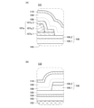
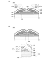
図1(A)は、トランジスタ100の平面図である。図1(B)は、図1(A)に記したX1−X2の一点鎖線で示す部位の断面図である。図1(C)は、図1(A)に記したY1−Y2の一点鎖線で示す部位の断面図である。図2(A)は、図1(B)に示した部位131の拡大図である。図2(B)は、図1(C)に示した部位132の拡大図である。
電極102は、ゲート電極として機能できる。電極102に加えて電極121をトランジスタ100に設ける場合、電極121もゲート電極として機能できる。電極102または電極121の一方を、「ゲート電極」という場合、他方を「バックゲート電極」という。例えば、図6(A)または図6(C)に示すトランジスタ100において、電極102を「ゲート電極」と言う場合、電極121を「バックゲート電極」と言う。電極121を「ゲート電極」として用いる場合は、トランジスタ100をトップゲート型のトランジスタの一種と考えることができる。電極102および電極121のどちらか一方を、「第1のゲート電極」といい、他方を「第2のゲート電極」という場合がある。
基板101としては、ガラス基板、セラミック基板の他、本作製工程の処理温度に耐えうる程度の耐熱性を有する可撓性基板(フレキシブル基板)等を用いることができる。また、基板に透光性を要しない場合には、ステンレス合金等の金属の基板の表面に絶縁層を設けたものを用いてもよい。ガラス基板としては、例えば、バリウムホウケイ酸ガラス、アルミノホウケイ酸ガラス若しくはアルミノケイ酸ガラス等の無アルカリガラス基板を用いるとよい。他に、石英基板、サファイア基板などを用いることができる。
絶縁層103乃至絶縁層105、絶縁層108、絶縁層109、絶縁層110、絶縁層111、絶縁層113は、窒化アルミニウム、酸化アルミニウム、窒化酸化アルミニウム、酸化窒化アルミニウム、酸化マグネシウム、窒化シリコン、酸化シリコン、窒化酸化シリコン、酸化窒化シリコン、酸化ガリウム、酸化ゲルマニウム、酸化イットリウム、酸化ジルコニウム、酸化ランタン、酸化ネオジム、酸化ハフニウム、酸化タンタル、アルミニウムシリケートなどから選ばれた材料を、単層でまたは積層して用いる。また、酸化物材料、窒化物材料、酸化窒化物材料、窒化酸化物材料のうち、複数の材料を混合した材料を用いてもよい。
電極102、電極107a_1、電極107a_2、電極107a_3、電極107b_1、電極107b_2、電極107b_3、および電極121を形成するための導電性材料としては、アルミニウム(Al)、クロム(Cr)、銅(Cu)、銀(Ag)、金(Au)、白金(Pt)、タンタル(Ta)、ニッケル(Ni)、チタン(Ti)、モリブデン(Mo)、タングステン(W)、ハフニウム(Hf)、バナジウム(V)、ニオブ(Nb)、マンガン(Mn)、マグネシウム(Mg)、ジルコニウム(Zr)、ベリリウム(Be)などから選ばれた金属元素を1種以上含む材料を用いることができる。また、リン等の不純物元素を含有させた多結晶シリコンに代表される、電気伝導度が高い半導体、ニッケルシリサイドなどのシリサイドを用いてもよい。
酸化物半導体層106として、酸化物半導体を用いることが好ましい。酸化物半導体のバンドギャップは2eV以上あるため、酸化物半導体層106に酸化物半導体を用いると、オフ電流が極めて少ないトランジスタを実現することができる。また、チャネルが形成される半導体層に酸化物半導体を用いたトランジスタ(「OSトランジスタ」ともいう。)は、ソースとドレイン間の絶縁耐圧が高い。よって、信頼性の良好なトランジスタを提供できる。また、出力電圧が大きく高耐圧なトランジスタを提供できる。また、信頼性の良好な半導体装置などを提供できる。また、出力電圧が大きく高耐圧な半導体装置を提供することができる。
次に、酸化物半導体膜の区分について説明する。
CAAC−OS膜は、c軸配向した複数の結晶部(ペレットともいう。)を有する酸化物半導体膜の一種である。
nc−OSをXRDによって解析した場合について説明する。例えば、nc−OSに対し、out−of−plane法による構造解析を行うと、配向性を示すピークが現れない。即ち、nc−OSの結晶は配向性を有さない。
a−like OS膜は、nc−OS膜と非晶質酸化物半導体膜との間の構造を有する酸化物半導体膜である。
絶縁層、電極や配線を形成するための導電層、または半導体層などは、スパッタリング法、スピンコート法、CVD(Chemical Vapor Deposition)法(熱CVD法、MOCVD(Metal Organic Chemical Vapor Deposition)法、PECVD(Plasma Enhanced CVD)法、高密度プラズマCVD(High density plasma CVD)法、LPCVD法(low pressure CVD)、APCVD法(atmospheric pressure CVD)等を含む)、ALD(Atomic Layer Deposition)法、または、MBE(Molecular Beam Epitaxy)法、または、PLD(Pulsed Laser Deposition)法、ディップ法、スプレー塗布法、液滴吐出法(インクジェット法など)、印刷法(スクリーン印刷、オフセット印刷など)を用いて形成することができる。
図1および図2に示すトランジスタ100の作製方法例について図7(A)乃至図7(D)、図8(A)乃至図8(C)、図9(A)乃至図9(C)および図10(A)乃至図10(C)を用いて説明する。図7(A)乃至図7(D)、図8(A)乃至図8(C)、図9(A)乃至図9(C)および図10(A)乃至図10(C)中のX1−X2断面は、図1(A)にX1−X2の一点鎖線で示す部位の断面に相当する。
まず、基板101上に電極102を形成するための導電層181を形成する(図7(A)参照。)。本実施の形態では、基板101としてアルミノホウケイ酸ガラスを用いる。また、本実施の形態では、導電層181として厚さ50nmのチタン層と、厚さ200nmの銅層とを、それぞれ順にスパッタリング法により形成する。
次に、レジストマスクを形成する(図示せず。)。レジストマスクの形成は、フォトリソグラフィ法、印刷法、インクジェット法等を適宜用いて行うことができる。レジストマスクを印刷法やインクジェット法などで形成すると、フォトマスクを使用しないため製造コストを低減できる。
次に、絶縁層103、絶縁層104、および絶縁層105を順に形成する(図7(C)参照。)。本実施の形態では、絶縁層103として厚さ400nmの窒化シリコン層を形成し、絶縁層104として厚さ30nmの酸化アルミニウム層を形成し、絶縁層105として厚さ50nmの酸化窒化シリコン層を形成する。
次に、酸化物半導体層182と酸化物半導体層183を順に形成する(図7(D)参照。)。なお、酸化物半導体層182を形成する前に、酸素ガスを供給してプラズマを発生させてもよい。このことにより、酸化物半導体層182の被形成面となる絶縁層105中に酸素を添加できる。
次に、フォトリソグラフィ法によりレジストマスクを形成する(図示せず。)。当該レジストマスクをマスクとして用いて、酸化物半導体層182および酸化物半導体層183の一部を選択的に除去して、島状の酸化物半導体層106_1および島状の酸化物半導体層106_2を形成する(図8(A)参照。)。
次に、導電層184および導電層185を順に形成する(図8(B)参照。)。導電層184は、酸化物半導体層106と接するため、加熱処理により水素を吸収する機能を有する導電性材料を用いることが好ましい。導電層184にこのような材料を用いることで、後の加熱処理によって、酸化物半導体層106中の水素濃度を低減することができる。水素を吸収する機能を有する導電性材料の一例として、チタン、インジウム亜鉛酸化物、シリコンを添加したインジウム錫酸化物などがある。
次に、フォトリソグラフィ法によりレジストマスクを形成する(図示せず。)。当該レジストマスクをマスクとして用いて、導電層185の一部を選択的に除去して、電極107a_2および電極107b_2を形成する(図8(C)参照。)。
次に、導電層186を形成する(図9(A)参照。)。本実施の形態では、導電層186として厚さ10nmのチタン層を形成する。
次に、フォトリソグラフィ法によりレジストマスクを形成する(図示せず。)。当該レジストマスクをマスクとして用いて、導電層184および導電層186の一部を選択的に除去して、電極107a_1、電極107a_3、電極107b_1、および電極107b_3を形成する(図9(B)参照。)。このようにして電極107aおよび電極107bが形成される。
次に、絶縁層108と絶縁層109を順に形成する(図9(C)参照。)。絶縁層108と絶縁層109は、途中で大気に曝すことなく連続して形成することが好ましい。
次に、不活性雰囲気下で加熱処理を行ない、絶縁層108および絶縁層109中に含まれる水素や水分などの不純物を低減する。なお、不活性ガスなどのガス供給を行なわず、減圧下で加熱処理を行なってもよい。本実施の形態では、窒素雰囲気中で400℃、1時間の加熱処理をおこなう(図10(A)参照。)。
続けて、酸化性雰囲気中で加熱処理を行なう。本実施の形態では、酸素雰囲気中で400℃、1時間の加熱処理をおこなう(図10(B)参照。)。工程11および工程12において、絶縁層108および/または絶縁層109に含まれる酸素の一部を酸化物半導体層106に移動させ、酸化物半導体層106に含まれる酸素欠損を低減することができる。なお、工程11または工程12の一方を省略してもよい。
次に、絶縁層110を形成する(図10(C)参照。)。前述した通り、絶縁層110は、不純物が透過しにくい絶縁性材料を用いて形成することが好ましい。また、絶縁層110は、酸素が拡散しにくい絶縁性材料を用いて形成することが好ましい。絶縁層110の厚さは5nm乃至40nmであればよい。
トランジスタ100の変形例について図面を用いて説明する。
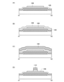
図11(A)は、トランジスタ100Aの平面図である。図11(B)は、図11(A)に記したX1−X2の一点鎖線で示す部位の断面図である。図11(C)は、図11(A)に記したY1−Y2の一点鎖線で示す部位の断面図である。
図12(A)は、トランジスタ100Bの平面図である。図12(B)は、図12(A)に記したX1−X2の一点鎖線で示す部位の断面図である。図12(C)は、図12(A)に記したY1−Y2の一点鎖線で示す部位の断面図である。図13(A)は、図12(B)に示した部位131Bの拡大図である。図13(B)は、図12(C)に示した部位132Bの拡大図である。
図14(A)は、トランジスタ100Cの平面図である。図14(B)は、図14(A)に記したX1−X2の一点鎖線で示す部位の断面図である。図14(C)は、図14(A)に記したY1−Y2の一点鎖線で示す部位の断面図である。図15(A)は、図14(B)に示した部位131Cの拡大図である。図15(B)は、図14(C)に示した部位132Cの拡大図である。
図16(A)は、トランジスタ100Dの平面図である。図16(B)は、図16(A)に記したX1−X2の一点鎖線で示す部位の断面図である。図16(C)は、図16(A)に記したY1−Y2の一点鎖線で示す部位の断面図である。図17(A)は、図16(B)に示した部位131Dの拡大図である。図17(B)は、図16(C)に示した部位132Dの拡大図である。
本発明の一態様のトランジスタ200について、図面を用いて説明する。
図19(A)は、トランジスタ200の平面図である。図19(B)は、図19(A)に記したX1−X2の一点鎖線で示す部位の断面図である。図19(C)は、図19(A)に記したY1−Y2の一点鎖線で示す部位の断面図である。図20は、図19(B)に示した部位231の拡大図である。
トランジスタ200の作製方法例について図23(A)乃至図26(C)を用いて説明する。図23(A)乃至図26(C)中のX1−X2断面は、図19(A)にX1−X2の一点鎖線で示す部位の断面に相当する。
まず、基板101上に電極102を形成するための導電層181を形成する(図23(A)参照。)。本実施の形態では、基板101としてアルミノホウケイ酸ガラスを用いる。また、本実施の形態では、導電層181として厚さ50nmのチタン層と、厚さ200nmの銅層とを、それぞれ順にスパッタリング法により形成する。
次に、レジストマスクを形成する(図示せず。)。レジストマスクの形成は、フォトリソグラフィ法、印刷法、インクジェット法等を適宜用いて行うことができる。レジストマスクを印刷法やインクジェット法などで形成すると、フォトマスクを使用しないため製造コストを低減できる。
次に、絶縁層103、絶縁層104、および絶縁層105を順に形成する(図23(C)参照。)。本実施の形態では、絶縁層103として厚さ400nmの窒化シリコン層を形成し、絶縁層104として厚さ30nmの酸化アルミニウム層を形成し、絶縁層105として厚さ50nmの酸化窒化シリコン層を形成する。
次に、酸化物半導体層182を形成する(図23(D)参照。)。なお、酸化物半導体層182を形成する前に、酸素ガスを供給してプラズマを発生させてもよい。このことにより、酸化物半導体層182の被形成面となる絶縁層105中に酸素を添加できる。
次に、フォトリソグラフィ法によりレジストマスクを形成する(図示せず。)。当該レジストマスクをマスクとして用いて、酸化物半導体層182の一部を選択的に除去して、島状の酸化物半導体層106を形成する(図24(A)参照。)。
次に、絶縁層108と絶縁層109を順に形成する(図24(B)参照。)。絶縁層108と絶縁層109は、途中で大気に曝すことなく連続して形成することが好ましい。
絶縁層109上に電極112を形成するための導電層185を形成する(図24(C)参照。)。本実施の形態では、導電層185としてインジウムガリウム亜鉛酸化物を用いる。より具体的には、導電層185としてインジウムガリウム亜鉛酸化物の二層積層を用いる。
次に、フォトリソグラフィ法によりレジストマスクを形成する(図示せず。)。当該レジストマスクをマスクとして用いて、導電層185の一部を選択的に除去して、電極112を形成する。この時、電極112をマスクとして用いて、絶縁層108と絶縁層109の一部も選択的に除去する(図24(D)参照。)。工程8により、酸化物半導体層106の一部が露出する。
次に、酸化物半導体層106の工程8で露出した領域に不純物を導入する(図25(A)参照。)。不純物の導入は、イオン注入法、イオンドーピング法、プラズマイマージョンイオン注入法などで行うことができる。当該領域に窒素などの不純物を導入することにより、当該領域の抵抗値を低下させることができる。
次に、不活性雰囲気下で加熱処理を行ない、酸化物半導体層106、絶縁層108および絶縁層109中に含まれる水素や水分などを低減する。また、工程9の後に加熱処理を行うことで、酸化物半導体層106のソース領域とドレイン領域の抵抗値が低下する場合がある。なお、加熱処理は不活性ガスなどのガス供給を行なわず、減圧下で行なってもよい。本実施の形態では、窒素雰囲気中で400℃、1時間の加熱処理をおこなう。
続けて、酸化性雰囲気中で加熱処理を行なってもよい。本実施の形態では、酸素雰囲気中で400℃、1時間の加熱処理をおこなう。例えば、工程8で酸化物半導体層106に窒素を導入した場合、酸素雰囲気中で加熱処理を行うことで、ソース領域およびドレイン領域のNOXが増加し、抵抗値が低下する場合がある。なお、工程10または工程11の一方を省略してもよい。
次に、絶縁層110を形成する(図25(B)参照。)。前述した通り、絶縁層110は、不純物が透過しにくい絶縁性材料を用いて形成することが好ましい。また、絶縁層110は、酸素が拡散しにくい絶縁性材料を用いて形成することが好ましい。絶縁層110の厚さは5nm乃至40nmであればよい。
次に、絶縁層113を形成する(図25(C)参照。)。本実施の形態では、絶縁層113として厚さ1.5μmのアクリル樹脂層を形成する。
次に、フォトリソグラフィ法によりレジストマスクを形成する(図示せず。)。当該レジストマスクをマスクとして用いて、絶縁層113および絶縁層110それぞれの一部を選択的に除去して、開口188を形成する(図26(A)参照。)。この時、酸化物半導体層106の一部が露出する。
次に、導電層186と導電層187を順に形成する(図26(B)参照。)。特に導電層186は、酸化物半導体層106と接するため、加熱処理により水素を吸収する機能を有する導電性材料を用いることが好ましい。導電層186にこのような材料を用いることで、後の加熱処理によって、酸化物半導体層106中の水素濃度を低減することができる。水素を吸収する機能を有する導電性材料の一例として、チタン、インジウム亜鉛酸化物、シリコンを添加したインジウム錫酸化物などがある。
次に、フォトリソグラフィ法によりレジストマスクを形成する(図示せず。)。当該レジストマスクをマスクとして用いて、導電層186の一部を選択的に除去して、電極114a_1および電極114b_1を形成する(図26(C)参照。)。同時に導電層187の一部を選択的に除去して、電極114a_2および電極114b_2を形成する。
トランジスタ200の変形例について図面を用いて説明する。
図27(A)は、トランジスタ200Aの平面図である。図27(B)は、図27(A)に記したX1−X2の一点鎖線で示す部位の断面図である。図27(C)は、図27(A)に記したY1−Y2の一点鎖線で示す部位の断面図である。
図28(A)は、トランジスタ200Bの平面図である。図28(B)は、図28(A)に記したX1−X2の一点鎖線で示す部位の断面図である。図28(C)は、図28(A)に記したY1−Y2の一点鎖線で示す部位の断面図である。図29(A)は、図28(B)に示した部位231Bの拡大図である。図29(B)は、図28(C)に示した部位232Bの拡大図である。
図30(A)は、トランジスタ200Cの平面図である。図30(B)は、図30(A)に記したX1−X2の一点鎖線で示す部位の断面図である。図30(C)は、図30(A)に記したY1−Y2の一点鎖線で示す部位の断面図である。
図31(A)は、トランジスタ200Dの平面図である。図31(B)は、図31(A)に記したX1−X2の一点鎖線で示す部位の断面図である。図31(C)は、図31(A)に記したY1−Y2の一点鎖線で示す部位の断面図である。
図32(A)は、トランジスタ200Eの平面図である。図32(B)は、図32(A)に記したX1−X2の一点鎖線で示す部位の断面図である。図32(C)は、図32(A)に記したY1−Y2の一点鎖線で示す部位の断面図である。図33は、図32(B)に示した部位231Eの拡大図である。
本実施の形態では、本明細書等に開示したトランジスタを用いた半導体装置の一例として、表示装置および表示モジュールについて説明する。
上述したトランジスタを用いることができる表示装置の一例を説明する。図34(A)は、表示装置500の構成例を説明するブロック図である。
表示装置500は、様々な形態を用いること、または様々な表示素子を有することが出来る。表示素子の一例としては、EL(エレクトロルミネッセンス)素子(有機EL素子、無機EL素子、または、有機物及び無機物を含むEL素子)、LED(白色LED、赤色LED、緑色LED、青色LEDなど)、トランジスタ(電流に応じて発光するトランジスタ)、電子放出素子、液晶素子、電子インク、電気泳動素子、グレーティングライトバルブ(GLV)、MEMS(マイクロ・エレクトロ・メカニカル・システム)を用いた表示素子、デジタルマイクロミラーデバイス(DMD)、DMS(デジタル・マイクロ・シャッター)、MIRASOL(登録商標)、IMOD(インターフェロメトリック・モジュレーション)素子、シャッター方式のMEMS表示素子、光干渉方式のMEMS表示素子、エレクトロウェッティング素子、圧電セラミックディスプレイ、カーボンナノチューブを用いた表示素子、など、電気的または磁気的作用により、コントラスト、輝度、反射率、透過率などが変化する表示媒体を有するものがある。また、表示素子として量子ドットを用いてもよい。
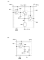
図34(B)に示す画素回路534は、トランジスタ461と、容量素子463と、トランジスタ468と、トランジスタ464と、を有する。また、図34(B)に示す画素回路534は、表示素子として機能できる発光素子469と電気的に接続されている。
図34(C)に示す画素回路534は、トランジスタ461と、容量素子463と、を有する。また、図34(C)に示す画素回路534は、表示素子として機能できる液晶素子462と電気的に接続されている。トランジスタ461にOSトランジスタを用いることが好ましい。
図36(A)に駆動回路511の構成例を示す。駆動回路511は、シフトレジスタ512、ラッチ回路513、およびバッファ514を有する。また、図36(B)に駆動回路521aの構成例を示す。駆動回路521aは、シフトレジスタ522、およびバッファ523を有する。駆動回路521bも駆動回路521aと同様の構成とすることができる。
上記実施の形態に示したトランジスタを用いて、シフトレジスタを含む駆動回路の一部または全体を画素部と同じ基板上に一体形成して、システムオンパネルを形成することができる。
上述したトランジスタを使用した半導体装置の一例として、表示モジュールについて説明する。図40に示す表示モジュール6000は、上部カバー6001と下部カバー6002との間に、FPC6003に接続されたタッチセンサ6004、FPC6005に接続された表示パネル6006、バックライトユニット6007、フレーム6009、プリント基板6010、バッテリ6011を有する。なお、バックライトユニット6007、バッテリ6011、タッチセンサ6004などは、設けられない場合もある。
本発明の一態様に係るトランジスタおよび/または半導体装置は、様々な電子機器に用いることができる。図41および図42に、本発明の一態様に係るトランジスタおよび/または半導体装置を用いた電子機器の例を示す。
101 基板
102 電極
103 絶縁層
104 絶縁層
105 絶縁層
106 酸化物半導体層
108 絶縁層
109 絶縁層
110 絶縁層
113 絶縁層
121 電極
131 部位
132 部位
181 導電層
182 酸化物半導体層
183 酸化物半導体層
184 導電層
185 導電層
186 導電層
200 トランジスタ
461 トランジスタ
462 液晶素子
463 容量素子
464 トランジスタ
465 ノード
466 ノード
467 ノード
468 トランジスタ
469 発光素子
500 表示装置
511 駆動回路
Claims (3)
- 第1乃至第3の電極と、第1乃至第5の絶縁層と、第1の酸化物半導体層および第2の酸化物半導体層と、を有し、
前記第1の絶縁層は、前記第1の電極の上にあり、
前記第2の絶縁層は、前記第1の絶縁層の上にあり、
前記第3の絶縁層は、前記第2の絶縁層の上にあり、
前記第1の酸化物半導体層は、前記第3の絶縁層の上にあり、
前記第2の酸化物半導体層は、前記第1の酸化物半導体層の上にあり、
前記第1の電極、前記第1の絶縁層、前記第2の絶縁層、前記第3の絶縁層、前記第1の酸化物半導体層、および前記第2の酸化物半導体層は、それぞれが互いに重なる領域を有し、
前記第2の電極は、前記第2の酸化物半導体層上で前記第2の酸化物半導体層と重なる領域と、前記第2の絶縁層上で前記第2の絶縁層と重なる領域と、を有し、
前記第3の電極は、前記第2の酸化物半導体層上で前記第2の酸化物半導体層と重なる領域と、前記第2の絶縁層上で前記第2の絶縁層と重なる領域と、を有し、
前記第4の絶縁層は、前記第2の酸化物半導体層と重なる領域を有し、
前記第5の絶縁層は、前記第4の絶縁層の上にあり、
前記第2の酸化物半導体層は結晶性を有し、
前記第2の電極は、第1の導電層と、前記第1の導電層の上にある第3の導電層と、前記第1の導電層及び前記第3の導電層により覆われた、銅を含む第2の導電層と、を有し、
前記第3の電極は、第4の導電層と、前記第4の導電層の上にある第6の導電層と、前記第4の導電層及び前記第6の導電層により覆われた、銅を含む第5の導電層と、を有し、
前記第2の絶縁層は、前記第3の絶縁層及び前記第4の絶縁層に設けられた開口を介して、前記第5の絶縁層と接する第1の領域を有し、
前記第1の酸化物半導体層及び前記第2の酸化物半導体層を平面図で見た場合に、前記第1の領域は、前記第1の酸化物半導体層及び前記第2の酸化物半導体層の外側を囲んでいる半導体装置。 - 請求項1において、
前記第2の絶縁層は、酸化アルミニウム、窒化アルミニウム、酸化窒化アルミニウム、窒化酸化アルミニウム、酸化ガリウム、酸化ゲルマニウム、酸化イットリウム、酸化ジルコニウム、酸化ランタン、酸化ネオジム、酸化ハフニウム、酸化タンタル、または窒化シリコンを有する半導体装置。 - 請求項1または請求項2において、
前記第5の絶縁層は、酸化アルミニウム、窒化アルミニウム、酸化窒化アルミニウム、窒化酸化アルミニウム、酸化ガリウム、酸化ゲルマニウム、酸化イットリウム、酸化ジルコニウム、酸化ランタン、酸化ネオジム、酸化ハフニウム、酸化タンタル、または窒化シリコンを有する半導体装置。
Priority Applications (1)
| Application Number | Priority Date | Filing Date | Title |
|---|---|---|---|
| JP2021195286A JP7270711B2 (ja) | 2016-04-08 | 2021-12-01 | 半導体装置 |
Applications Claiming Priority (4)
| Application Number | Priority Date | Filing Date | Title |
|---|---|---|---|
| JP2016078347 | 2016-04-08 | ||
| JP2016078286 | 2016-04-08 | ||
| JP2016078286 | 2016-04-08 | ||
| JP2016078347 | 2016-04-08 |
Related Child Applications (1)
| Application Number | Title | Priority Date | Filing Date |
|---|---|---|---|
| JP2021195286A Division JP7270711B2 (ja) | 2016-04-08 | 2021-12-01 | 半導体装置 |
Publications (3)
| Publication Number | Publication Date |
|---|---|
| JP2017191934A JP2017191934A (ja) | 2017-10-19 |
| JP2017191934A5 JP2017191934A5 (ja) | 2020-05-14 |
| JP6987520B2 true JP6987520B2 (ja) | 2022-01-05 |
Family
ID=59998845
Family Applications (3)
| Application Number | Title | Priority Date | Filing Date |
|---|---|---|---|
| JP2017074988A Active JP6987520B2 (ja) | 2016-04-08 | 2017-04-05 | 半導体装置 |
| JP2021195286A Active JP7270711B2 (ja) | 2016-04-08 | 2021-12-01 | 半導体装置 |
| JP2023071278A Pending JP2023099557A (ja) | 2016-04-08 | 2023-04-25 | 半導体装置 |
Family Applications After (2)
| Application Number | Title | Priority Date | Filing Date |
|---|---|---|---|
| JP2021195286A Active JP7270711B2 (ja) | 2016-04-08 | 2021-12-01 | 半導体装置 |
| JP2023071278A Pending JP2023099557A (ja) | 2016-04-08 | 2023-04-25 | 半導体装置 |
Country Status (2)
| Country | Link |
|---|---|
| US (3) | US11302717B2 (ja) |
| JP (3) | JP6987520B2 (ja) |
Families Citing this family (8)
| Publication number | Priority date | Publication date | Assignee | Title |
|---|---|---|---|---|
| WO2019087002A1 (ja) | 2017-11-02 | 2019-05-09 | 株式会社半導体エネルギー研究所 | 半導体装置 |
| KR102550633B1 (ko) * | 2018-05-04 | 2023-07-04 | 삼성디스플레이 주식회사 | 박막 트랜지스터 기판 및 그 제조방법 |
| US11251224B2 (en) * | 2018-10-31 | 2022-02-15 | Samsung Display Co., Ltd. | Display device and method of fabricating the same |
| JP7475282B2 (ja) | 2018-11-02 | 2024-04-26 | 株式会社半導体エネルギー研究所 | 半導体装置 |
| TW202133465A (zh) * | 2020-02-14 | 2021-09-01 | 晶元光電股份有限公司 | 聲波元件及其形成方法 |
| US20210376156A1 (en) * | 2020-05-29 | 2021-12-02 | Taiwan Semiconductor Manufacturing Company Limited | Raised source/drain oxide semiconducting thin film transistor and methods of making the same |
| CN112882606B (zh) * | 2021-03-04 | 2022-12-27 | 业成科技(成都)有限公司 | 触控面板 |
| JP7410261B1 (ja) | 2022-12-08 | 2024-01-09 | 日機装株式会社 | 半導体発光素子および半導体発光素子の製造方法 |
Family Cites Families (74)
| Publication number | Priority date | Publication date | Assignee | Title |
|---|---|---|---|---|
| JP3537854B2 (ja) * | 1992-12-29 | 2004-06-14 | エルジー フィリップス エルシーディー カンパニー リミテッド | 薄膜トランジスタの製造方法 |
| JP4108633B2 (ja) * | 2003-06-20 | 2008-06-25 | シャープ株式会社 | 薄膜トランジスタおよびその製造方法ならびに電子デバイス |
| TWI336921B (en) * | 2003-07-18 | 2011-02-01 | Semiconductor Energy Lab | Method for manufacturing semiconductor device |
| WO2005041311A1 (en) * | 2003-10-28 | 2005-05-06 | Semiconductor Energy Laboratory Co., Ltd. | Liquid crystal display device and method for manufacturing the same, and liquid crystal television reciever |
| CN1871711B (zh) * | 2003-10-28 | 2011-12-07 | 株式会社半导体能源研究所 | 显示器件及其制造方法,以及电视接收机 |
| US7592207B2 (en) * | 2003-11-14 | 2009-09-22 | Semiconductor Energy Laboratory Co., Ltd. | Light-emitting device and method for manufacturing the same |
| JP5126729B2 (ja) | 2004-11-10 | 2013-01-23 | キヤノン株式会社 | 画像表示装置 |
| US7791072B2 (en) | 2004-11-10 | 2010-09-07 | Canon Kabushiki Kaisha | Display |
| TWI505473B (zh) * | 2005-01-28 | 2015-10-21 | Semiconductor Energy Lab | 半導體裝置,電子裝置,和半導體裝置的製造方法 |
| US8900970B2 (en) * | 2006-04-28 | 2014-12-02 | Semiconductor Energy Laboratory Co., Ltd. | Method for manufacturing a semiconductor device using a flexible substrate |
| KR101345376B1 (ko) * | 2007-05-29 | 2013-12-24 | 삼성전자주식회사 | ZnO 계 박막 트랜지스터 및 그 제조방법 |
| US20090278120A1 (en) * | 2008-05-09 | 2009-11-12 | Korea Institute Of Science And Technology | Thin Film Transistor |
| KR100963027B1 (ko) * | 2008-06-30 | 2010-06-10 | 삼성모바일디스플레이주식회사 | 박막 트랜지스터, 그의 제조 방법 및 박막 트랜지스터를구비하는 평판 표시 장치 |
| TWI622175B (zh) * | 2008-07-31 | 2018-04-21 | 半導體能源研究所股份有限公司 | 半導體裝置 |
| TWI711182B (zh) * | 2008-07-31 | 2020-11-21 | 日商半導體能源研究所股份有限公司 | 半導體裝置及半導體裝置的製造方法 |
| US9666719B2 (en) * | 2008-07-31 | 2017-05-30 | Semiconductor Energy Laboratory Co., Ltd. | Semiconductor device and manufacturing method thereof |
| US8945981B2 (en) * | 2008-07-31 | 2015-02-03 | Semiconductor Energy Laboratory Co., Ltd. | Semiconductor device and manufacturing method thereof |
| TWI518800B (zh) * | 2008-08-08 | 2016-01-21 | 半導體能源研究所股份有限公司 | 半導體裝置的製造方法 |
| KR20100023151A (ko) * | 2008-08-21 | 2010-03-04 | 삼성모바일디스플레이주식회사 | 박막 트랜지스터 및 그 제조방법 |
| KR101774212B1 (ko) * | 2008-09-19 | 2017-09-04 | 가부시키가이샤 한도오따이 에네루기 켄큐쇼 | 반도체 장치 |
| CN101714546B (zh) * | 2008-10-03 | 2014-05-14 | 株式会社半导体能源研究所 | 显示装置及其制造方法 |
| JP5552753B2 (ja) * | 2008-10-08 | 2014-07-16 | ソニー株式会社 | 薄膜トランジスタおよび表示装置 |
| JP5361651B2 (ja) * | 2008-10-22 | 2013-12-04 | 株式会社半導体エネルギー研究所 | 半導体装置の作製方法 |
| US8704216B2 (en) * | 2009-02-27 | 2014-04-22 | Semiconductor Energy Laboratory Co., Ltd. | Semiconductor device and manufacturing method thereof |
| WO2011007677A1 (en) | 2009-07-17 | 2011-01-20 | Semiconductor Energy Laboratory Co., Ltd. | Semiconductor device and method for manufacturing the same |
| WO2011027723A1 (en) | 2009-09-04 | 2011-03-10 | Semiconductor Energy Laboratory Co., Ltd. | Semiconductor device and method for manufacturing the same |
| CN105679766A (zh) * | 2009-09-16 | 2016-06-15 | 株式会社半导体能源研究所 | 晶体管及显示设备 |
| JP5679143B2 (ja) * | 2009-12-01 | 2015-03-04 | ソニー株式会社 | 薄膜トランジスタならびに表示装置および電子機器 |
| KR20120103676A (ko) | 2009-12-04 | 2012-09-19 | 가부시키가이샤 한도오따이 에네루기 켄큐쇼 | 반도체 장치 |
| EP2510541A4 (en) * | 2009-12-11 | 2016-04-13 | Semiconductor Energy Lab | NONVOLATILE LATCH CIRCUIT, LOGIC CIRCUIT, AND SEMICONDUCTOR DEVICE USING THE SAME |
| US20120248450A1 (en) * | 2009-12-17 | 2012-10-04 | Sharp Kabushiki Kaisha | Active matrix substrate and method for producing same |
| KR101760537B1 (ko) * | 2009-12-28 | 2017-07-21 | 가부시키가이샤 한도오따이 에네루기 켄큐쇼 | 반도체 장치 |
| KR20130014562A (ko) * | 2010-04-02 | 2013-02-07 | 가부시키가이샤 한도오따이 에네루기 켄큐쇼 | 반도체 장치 |
| US9147768B2 (en) * | 2010-04-02 | 2015-09-29 | Semiconductor Energy Laboratory Co., Ltd. | Semiconductor device having an oxide semiconductor and a metal oxide film |
| US8629438B2 (en) * | 2010-05-21 | 2014-01-14 | Semiconductor Energy Laboratory Co., Ltd. | Semiconductor device and manufacturing method thereof |
| KR101862808B1 (ko) * | 2010-06-18 | 2018-05-30 | 가부시키가이샤 한도오따이 에네루기 켄큐쇼 | 반도체 장치 |
| KR101809105B1 (ko) | 2010-08-06 | 2017-12-14 | 가부시키가이샤 한도오따이 에네루기 켄큐쇼 | 반도체 집적 회로 |
| US9252279B2 (en) | 2011-08-31 | 2016-02-02 | Semiconductor Energy Laboratory Co., Ltd. | Semiconductor device and manufacturing method thereof |
| KR102100425B1 (ko) * | 2011-12-27 | 2020-04-13 | 가부시키가이샤 한도오따이 에네루기 켄큐쇼 | 반도체 장치 및 반도체 장치의 제작 방법 |
| WO2013111756A1 (en) * | 2012-01-25 | 2013-08-01 | Semiconductor Energy Laboratory Co., Ltd. | Semiconductor device and method for manufacturing semiconductor device |
| US20130207111A1 (en) | 2012-02-09 | 2013-08-15 | Semiconductor Energy Laboratory Co., Ltd. | Semiconductor device, display device including semiconductor device, electronic device including semiconductor device, and method for manufacturing semiconductor device |
| JP2013201428A (ja) | 2012-02-23 | 2013-10-03 | Semiconductor Energy Lab Co Ltd | 半導体装置の作製方法 |
| JP2013236068A (ja) * | 2012-04-12 | 2013-11-21 | Semiconductor Energy Lab Co Ltd | 半導体装置及び半導体装置の作製方法 |
| US9236408B2 (en) * | 2012-04-25 | 2016-01-12 | Semiconductor Energy Laboratory Co., Ltd. | Oxide semiconductor device including photodiode |
| US9006024B2 (en) * | 2012-04-25 | 2015-04-14 | Semiconductor Energy Laboratory Co., Ltd. | Method for manufacturing semiconductor device |
| KR102388690B1 (ko) * | 2012-05-31 | 2022-04-19 | 가부시키가이샤 한도오따이 에네루기 켄큐쇼 | 반도체 장치 |
| US9153699B2 (en) * | 2012-06-15 | 2015-10-06 | Semiconductor Energy Laboratory Co., Ltd. | Thin film transistor with multiple oxide semiconductor layers |
| US8901557B2 (en) * | 2012-06-15 | 2014-12-02 | Semiconductor Energy Laboratory Co., Ltd. | Semiconductor device |
| KR20220013471A (ko) | 2012-06-29 | 2022-02-04 | 가부시키가이샤 한도오따이 에네루기 켄큐쇼 | 액정 디스플레이 디바이스 |
| KR102161077B1 (ko) * | 2012-06-29 | 2020-09-29 | 가부시키가이샤 한도오따이 에네루기 켄큐쇼 | 반도체 장치 |
| JP6310194B2 (ja) * | 2012-07-06 | 2018-04-11 | 株式会社半導体エネルギー研究所 | 半導体装置 |
| JP6006558B2 (ja) * | 2012-07-17 | 2016-10-12 | 株式会社半導体エネルギー研究所 | 半導体装置及びその製造方法 |
| JP6134598B2 (ja) * | 2012-08-02 | 2017-05-24 | 株式会社半導体エネルギー研究所 | 半導体装置 |
| KR102171650B1 (ko) * | 2012-08-10 | 2020-10-29 | 가부시키가이샤 한도오따이 에네루기 켄큐쇼 | 반도체 장치 및 그 제작 방법 |
| JP6211843B2 (ja) * | 2012-08-10 | 2017-10-11 | 株式会社半導体エネルギー研究所 | 半導体装置 |
| US9245958B2 (en) * | 2012-08-10 | 2016-01-26 | Semiconductor Energy Laboratory Co., Ltd. | Semiconductor device and method for manufacturing the same |
| KR102279459B1 (ko) | 2012-10-24 | 2021-07-19 | 가부시키가이샤 한도오따이 에네루기 켄큐쇼 | 반도체 장치 및 그 제작 방법 |
| DE112013007567B3 (de) * | 2012-11-08 | 2018-11-15 | Semiconductor Energy Laboratory Co., Ltd. | Halbleitervorrichtungen mit einem Metalloxidfilm |
| TWI614813B (zh) | 2013-01-21 | 2018-02-11 | 半導體能源研究所股份有限公司 | 半導體裝置的製造方法 |
| JP6298662B2 (ja) * | 2013-03-14 | 2018-03-20 | 株式会社半導体エネルギー研究所 | 半導体装置 |
| US10566455B2 (en) * | 2013-03-28 | 2020-02-18 | Semiconductor Energy Laboratory Co., Ltd. | Semiconductor device and manufacturing method thereof |
| US20140299873A1 (en) | 2013-04-05 | 2014-10-09 | Semiconductor Energy Laboratory Co., Ltd. | Single-crystal oxide semiconductor, thin film, oxide stack, and formation method thereof |
| DE102014208859B4 (de) * | 2013-05-20 | 2021-03-11 | Semiconductor Energy Laboratory Co., Ltd. | Halbleitervorrichtung |
| JP6426379B2 (ja) | 2013-06-19 | 2018-11-21 | 株式会社半導体エネルギー研究所 | 半導体装置の作製方法 |
| KR102290801B1 (ko) * | 2013-06-21 | 2021-08-17 | 가부시키가이샤 한도오따이 에네루기 켄큐쇼 | 반도체 장치 및 그 제작 방법 |
| JP6232219B2 (ja) | 2013-06-28 | 2017-11-15 | 東京エレクトロン株式会社 | 多層保護膜の形成方法 |
| JP6386323B2 (ja) * | 2013-10-04 | 2018-09-05 | 株式会社半導体エネルギー研究所 | 半導体装置 |
| US9590111B2 (en) * | 2013-11-06 | 2017-03-07 | Semiconductor Energy Laboratory Co., Ltd. | Semiconductor device and display device including the semiconductor device |
| KR102186576B1 (ko) * | 2014-03-21 | 2020-12-04 | 삼성디스플레이 주식회사 | 액정 표시 패널 및 이의 제조 방법 |
| DE112015001878B4 (de) | 2014-04-18 | 2021-09-09 | Semiconductor Energy Laboratory Co., Ltd. | Halbleitervorrichtung und elektronisches Gerät |
| US9780226B2 (en) * | 2014-04-25 | 2017-10-03 | Semiconductor Energy Laboratory Co., Ltd. | Semiconductor device and manufacturing method thereof |
| TWI666776B (zh) | 2014-06-20 | 2019-07-21 | 日商半導體能源研究所股份有限公司 | 半導體裝置以及包括該半導體裝置的顯示裝置 |
| KR102582523B1 (ko) * | 2015-03-19 | 2023-09-26 | 가부시키가이샤 한도오따이 에네루기 켄큐쇼 | 반도체 장치 및 전자 기기 |
| US10056497B2 (en) * | 2015-04-15 | 2018-08-21 | Semiconductor Energy Laboratory Co., Ltd. | Semiconductor device and manufacturing method thereof |
-
2017
- 2017-04-03 US US15/477,446 patent/US11302717B2/en active Active
- 2017-04-05 JP JP2017074988A patent/JP6987520B2/ja active Active
-
2021
- 2021-12-01 JP JP2021195286A patent/JP7270711B2/ja active Active
-
2022
- 2022-03-17 US US17/696,988 patent/US20220208796A1/en not_active Abandoned
-
2023
- 2023-04-25 JP JP2023071278A patent/JP2023099557A/ja active Pending
- 2023-09-13 US US18/367,508 patent/US20240006418A1/en active Pending
Also Published As
| Publication number | Publication date |
|---|---|
| US20170294543A1 (en) | 2017-10-12 |
| JP2017191934A (ja) | 2017-10-19 |
| JP2022033861A (ja) | 2022-03-02 |
| US20240006418A1 (en) | 2024-01-04 |
| US11302717B2 (en) | 2022-04-12 |
| JP7270711B2 (ja) | 2023-05-10 |
| US20220208796A1 (en) | 2022-06-30 |
| JP2023099557A (ja) | 2023-07-13 |
Similar Documents
| Publication | Publication Date | Title |
|---|---|---|
| JP6877519B2 (ja) | 半導体装置 | |
| US11842901B2 (en) | Semiconductor device, manufacturing method thereof, display device, and electronic device | |
| JP6987520B2 (ja) | 半導体装置 | |
| JP7278354B2 (ja) | 半導体装置の作製方法 | |
| JP7026759B2 (ja) | 半導体装置 | |
| JP7191190B2 (ja) | 半導体装置 | |
| JP7126823B2 (ja) | 半導体装置の作製方法 | |
| US20180025918A1 (en) | Method for manufacturing transistor and display device | |
| JP6986862B2 (ja) | トランジスタ | |
| JP2021168390A (ja) | 半導体装置 | |
| JP6985812B2 (ja) | トランジスタの作製方法 | |
| JP7078354B2 (ja) | 半導体装置及びその作製方法 |
Legal Events
| Date | Code | Title | Description |
|---|---|---|---|
| A521 | Request for written amendment filed |
Free format text: JAPANESE INTERMEDIATE CODE: A523 Effective date: 20200331 |
|
| A621 | Written request for application examination |
Free format text: JAPANESE INTERMEDIATE CODE: A621 Effective date: 20200331 |
|
| A977 | Report on retrieval |
Free format text: JAPANESE INTERMEDIATE CODE: A971007 Effective date: 20210323 |
|
| A131 | Notification of reasons for refusal |
Free format text: JAPANESE INTERMEDIATE CODE: A131 Effective date: 20210330 |
|
| A521 | Request for written amendment filed |
Free format text: JAPANESE INTERMEDIATE CODE: A523 Effective date: 20210525 |
|
| A131 | Notification of reasons for refusal |
Free format text: JAPANESE INTERMEDIATE CODE: A131 Effective date: 20210720 |
|
| A521 | Request for written amendment filed |
Free format text: JAPANESE INTERMEDIATE CODE: A523 Effective date: 20210826 |
|
| TRDD | Decision of grant or rejection written | ||
| A01 | Written decision to grant a patent or to grant a registration (utility model) |
Free format text: JAPANESE INTERMEDIATE CODE: A01 Effective date: 20211109 |
|
| A61 | First payment of annual fees (during grant procedure) |
Free format text: JAPANESE INTERMEDIATE CODE: A61 Effective date: 20211201 |
|
| R150 | Certificate of patent or registration of utility model |
Ref document number: 6987520 Country of ref document: JP Free format text: JAPANESE INTERMEDIATE CODE: R150 |