JP6862095B2 - エピタキシャル成長装置用のチャンバ構成要素 - Google Patents
エピタキシャル成長装置用のチャンバ構成要素 Download PDFInfo
- Publication number
- JP6862095B2 JP6862095B2 JP2016061889A JP2016061889A JP6862095B2 JP 6862095 B2 JP6862095 B2 JP 6862095B2 JP 2016061889 A JP2016061889 A JP 2016061889A JP 2016061889 A JP2016061889 A JP 2016061889A JP 6862095 B2 JP6862095 B2 JP 6862095B2
- Authority
- JP
- Japan
- Prior art keywords
- susceptor
- substrate
- concave portion
- gas
- holes
- Prior art date
- Legal status (The legal status is an assumption and is not a legal conclusion. Google has not performed a legal analysis and makes no representation as to the accuracy of the status listed.)
- Active
Links
Images












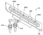

Classifications
-
- C—CHEMISTRY; METALLURGY
- C30—CRYSTAL GROWTH
- C30B—SINGLE-CRYSTAL GROWTH; UNIDIRECTIONAL SOLIDIFICATION OF EUTECTIC MATERIAL OR UNIDIRECTIONAL DEMIXING OF EUTECTOID MATERIAL; REFINING BY ZONE-MELTING OF MATERIAL; PRODUCTION OF A HOMOGENEOUS POLYCRYSTALLINE MATERIAL WITH DEFINED STRUCTURE; SINGLE CRYSTALS OR HOMOGENEOUS POLYCRYSTALLINE MATERIAL WITH DEFINED STRUCTURE; AFTER-TREATMENT OF SINGLE CRYSTALS OR A HOMOGENEOUS POLYCRYSTALLINE MATERIAL WITH DEFINED STRUCTURE; APPARATUS THEREFOR
- C30B25/00—Single-crystal growth by chemical reaction of reactive gases, e.g. chemical vapour-deposition growth
- C30B25/02—Epitaxial-layer growth
- C30B25/08—Reaction chambers; Selection of materials therefor
-
- C—CHEMISTRY; METALLURGY
- C23—COATING METALLIC MATERIAL; COATING MATERIAL WITH METALLIC MATERIAL; CHEMICAL SURFACE TREATMENT; DIFFUSION TREATMENT OF METALLIC MATERIAL; COATING BY VACUUM EVAPORATION, BY SPUTTERING, BY ION IMPLANTATION OR BY CHEMICAL VAPOUR DEPOSITION, IN GENERAL; INHIBITING CORROSION OF METALLIC MATERIAL OR INCRUSTATION IN GENERAL
- C23C—COATING METALLIC MATERIAL; COATING MATERIAL WITH METALLIC MATERIAL; SURFACE TREATMENT OF METALLIC MATERIAL BY DIFFUSION INTO THE SURFACE, BY CHEMICAL CONVERSION OR SUBSTITUTION; COATING BY VACUUM EVAPORATION, BY SPUTTERING, BY ION IMPLANTATION OR BY CHEMICAL VAPOUR DEPOSITION, IN GENERAL
- C23C16/00—Chemical coating by decomposition of gaseous compounds, without leaving reaction products of surface material in the coating, i.e. chemical vapour deposition [CVD] processes
- C23C16/44—Chemical coating by decomposition of gaseous compounds, without leaving reaction products of surface material in the coating, i.e. chemical vapour deposition [CVD] processes characterised by the method of coating
- C23C16/54—Apparatus specially adapted for continuous coating
-
- C—CHEMISTRY; METALLURGY
- C23—COATING METALLIC MATERIAL; COATING MATERIAL WITH METALLIC MATERIAL; CHEMICAL SURFACE TREATMENT; DIFFUSION TREATMENT OF METALLIC MATERIAL; COATING BY VACUUM EVAPORATION, BY SPUTTERING, BY ION IMPLANTATION OR BY CHEMICAL VAPOUR DEPOSITION, IN GENERAL; INHIBITING CORROSION OF METALLIC MATERIAL OR INCRUSTATION IN GENERAL
- C23C—COATING METALLIC MATERIAL; COATING MATERIAL WITH METALLIC MATERIAL; SURFACE TREATMENT OF METALLIC MATERIAL BY DIFFUSION INTO THE SURFACE, BY CHEMICAL CONVERSION OR SUBSTITUTION; COATING BY VACUUM EVAPORATION, BY SPUTTERING, BY ION IMPLANTATION OR BY CHEMICAL VAPOUR DEPOSITION, IN GENERAL
- C23C16/00—Chemical coating by decomposition of gaseous compounds, without leaving reaction products of surface material in the coating, i.e. chemical vapour deposition [CVD] processes
- C23C16/44—Chemical coating by decomposition of gaseous compounds, without leaving reaction products of surface material in the coating, i.e. chemical vapour deposition [CVD] processes characterised by the method of coating
- C23C16/455—Chemical coating by decomposition of gaseous compounds, without leaving reaction products of surface material in the coating, i.e. chemical vapour deposition [CVD] processes characterised by the method of coating characterised by the method used for introducing gases into reaction chamber or for modifying gas flows in reaction chamber
- C23C16/45502—Flow conditions in reaction chamber
-
- C—CHEMISTRY; METALLURGY
- C23—COATING METALLIC MATERIAL; COATING MATERIAL WITH METALLIC MATERIAL; CHEMICAL SURFACE TREATMENT; DIFFUSION TREATMENT OF METALLIC MATERIAL; COATING BY VACUUM EVAPORATION, BY SPUTTERING, BY ION IMPLANTATION OR BY CHEMICAL VAPOUR DEPOSITION, IN GENERAL; INHIBITING CORROSION OF METALLIC MATERIAL OR INCRUSTATION IN GENERAL
- C23C—COATING METALLIC MATERIAL; COATING MATERIAL WITH METALLIC MATERIAL; SURFACE TREATMENT OF METALLIC MATERIAL BY DIFFUSION INTO THE SURFACE, BY CHEMICAL CONVERSION OR SUBSTITUTION; COATING BY VACUUM EVAPORATION, BY SPUTTERING, BY ION IMPLANTATION OR BY CHEMICAL VAPOUR DEPOSITION, IN GENERAL
- C23C16/00—Chemical coating by decomposition of gaseous compounds, without leaving reaction products of surface material in the coating, i.e. chemical vapour deposition [CVD] processes
- C23C16/44—Chemical coating by decomposition of gaseous compounds, without leaving reaction products of surface material in the coating, i.e. chemical vapour deposition [CVD] processes characterised by the method of coating
- C23C16/455—Chemical coating by decomposition of gaseous compounds, without leaving reaction products of surface material in the coating, i.e. chemical vapour deposition [CVD] processes characterised by the method of coating characterised by the method used for introducing gases into reaction chamber or for modifying gas flows in reaction chamber
- C23C16/45563—Gas nozzles
- C23C16/45565—Shower nozzles
-
- C—CHEMISTRY; METALLURGY
- C23—COATING METALLIC MATERIAL; COATING MATERIAL WITH METALLIC MATERIAL; CHEMICAL SURFACE TREATMENT; DIFFUSION TREATMENT OF METALLIC MATERIAL; COATING BY VACUUM EVAPORATION, BY SPUTTERING, BY ION IMPLANTATION OR BY CHEMICAL VAPOUR DEPOSITION, IN GENERAL; INHIBITING CORROSION OF METALLIC MATERIAL OR INCRUSTATION IN GENERAL
- C23C—COATING METALLIC MATERIAL; COATING MATERIAL WITH METALLIC MATERIAL; SURFACE TREATMENT OF METALLIC MATERIAL BY DIFFUSION INTO THE SURFACE, BY CHEMICAL CONVERSION OR SUBSTITUTION; COATING BY VACUUM EVAPORATION, BY SPUTTERING, BY ION IMPLANTATION OR BY CHEMICAL VAPOUR DEPOSITION, IN GENERAL
- C23C16/00—Chemical coating by decomposition of gaseous compounds, without leaving reaction products of surface material in the coating, i.e. chemical vapour deposition [CVD] processes
- C23C16/44—Chemical coating by decomposition of gaseous compounds, without leaving reaction products of surface material in the coating, i.e. chemical vapour deposition [CVD] processes characterised by the method of coating
- C23C16/455—Chemical coating by decomposition of gaseous compounds, without leaving reaction products of surface material in the coating, i.e. chemical vapour deposition [CVD] processes characterised by the method of coating characterised by the method used for introducing gases into reaction chamber or for modifying gas flows in reaction chamber
- C23C16/45563—Gas nozzles
- C23C16/4558—Perforated rings
-
- C—CHEMISTRY; METALLURGY
- C23—COATING METALLIC MATERIAL; COATING MATERIAL WITH METALLIC MATERIAL; CHEMICAL SURFACE TREATMENT; DIFFUSION TREATMENT OF METALLIC MATERIAL; COATING BY VACUUM EVAPORATION, BY SPUTTERING, BY ION IMPLANTATION OR BY CHEMICAL VAPOUR DEPOSITION, IN GENERAL; INHIBITING CORROSION OF METALLIC MATERIAL OR INCRUSTATION IN GENERAL
- C23C—COATING METALLIC MATERIAL; COATING MATERIAL WITH METALLIC MATERIAL; SURFACE TREATMENT OF METALLIC MATERIAL BY DIFFUSION INTO THE SURFACE, BY CHEMICAL CONVERSION OR SUBSTITUTION; COATING BY VACUUM EVAPORATION, BY SPUTTERING, BY ION IMPLANTATION OR BY CHEMICAL VAPOUR DEPOSITION, IN GENERAL
- C23C16/00—Chemical coating by decomposition of gaseous compounds, without leaving reaction products of surface material in the coating, i.e. chemical vapour deposition [CVD] processes
- C23C16/44—Chemical coating by decomposition of gaseous compounds, without leaving reaction products of surface material in the coating, i.e. chemical vapour deposition [CVD] processes characterised by the method of coating
- C23C16/455—Chemical coating by decomposition of gaseous compounds, without leaving reaction products of surface material in the coating, i.e. chemical vapour deposition [CVD] processes characterised by the method of coating characterised by the method used for introducing gases into reaction chamber or for modifying gas flows in reaction chamber
- C23C16/45587—Mechanical means for changing the gas flow
-
- C—CHEMISTRY; METALLURGY
- C23—COATING METALLIC MATERIAL; COATING MATERIAL WITH METALLIC MATERIAL; CHEMICAL SURFACE TREATMENT; DIFFUSION TREATMENT OF METALLIC MATERIAL; COATING BY VACUUM EVAPORATION, BY SPUTTERING, BY ION IMPLANTATION OR BY CHEMICAL VAPOUR DEPOSITION, IN GENERAL; INHIBITING CORROSION OF METALLIC MATERIAL OR INCRUSTATION IN GENERAL
- C23C—COATING METALLIC MATERIAL; COATING MATERIAL WITH METALLIC MATERIAL; SURFACE TREATMENT OF METALLIC MATERIAL BY DIFFUSION INTO THE SURFACE, BY CHEMICAL CONVERSION OR SUBSTITUTION; COATING BY VACUUM EVAPORATION, BY SPUTTERING, BY ION IMPLANTATION OR BY CHEMICAL VAPOUR DEPOSITION, IN GENERAL
- C23C16/00—Chemical coating by decomposition of gaseous compounds, without leaving reaction products of surface material in the coating, i.e. chemical vapour deposition [CVD] processes
- C23C16/44—Chemical coating by decomposition of gaseous compounds, without leaving reaction products of surface material in the coating, i.e. chemical vapour deposition [CVD] processes characterised by the method of coating
- C23C16/455—Chemical coating by decomposition of gaseous compounds, without leaving reaction products of surface material in the coating, i.e. chemical vapour deposition [CVD] processes characterised by the method of coating characterised by the method used for introducing gases into reaction chamber or for modifying gas flows in reaction chamber
- C23C16/45587—Mechanical means for changing the gas flow
- C23C16/45591—Fixed means, e.g. wings, baffles
-
- C—CHEMISTRY; METALLURGY
- C23—COATING METALLIC MATERIAL; COATING MATERIAL WITH METALLIC MATERIAL; CHEMICAL SURFACE TREATMENT; DIFFUSION TREATMENT OF METALLIC MATERIAL; COATING BY VACUUM EVAPORATION, BY SPUTTERING, BY ION IMPLANTATION OR BY CHEMICAL VAPOUR DEPOSITION, IN GENERAL; INHIBITING CORROSION OF METALLIC MATERIAL OR INCRUSTATION IN GENERAL
- C23C—COATING METALLIC MATERIAL; COATING MATERIAL WITH METALLIC MATERIAL; SURFACE TREATMENT OF METALLIC MATERIAL BY DIFFUSION INTO THE SURFACE, BY CHEMICAL CONVERSION OR SUBSTITUTION; COATING BY VACUUM EVAPORATION, BY SPUTTERING, BY ION IMPLANTATION OR BY CHEMICAL VAPOUR DEPOSITION, IN GENERAL
- C23C16/00—Chemical coating by decomposition of gaseous compounds, without leaving reaction products of surface material in the coating, i.e. chemical vapour deposition [CVD] processes
- C23C16/44—Chemical coating by decomposition of gaseous compounds, without leaving reaction products of surface material in the coating, i.e. chemical vapour deposition [CVD] processes characterised by the method of coating
- C23C16/458—Chemical coating by decomposition of gaseous compounds, without leaving reaction products of surface material in the coating, i.e. chemical vapour deposition [CVD] processes characterised by the method of coating characterised by the method used for supporting substrates in the reaction chamber
- C23C16/4581—Chemical coating by decomposition of gaseous compounds, without leaving reaction products of surface material in the coating, i.e. chemical vapour deposition [CVD] processes characterised by the method of coating characterised by the method used for supporting substrates in the reaction chamber characterised by material of construction or surface finish of the means for supporting the substrate
-
- C—CHEMISTRY; METALLURGY
- C23—COATING METALLIC MATERIAL; COATING MATERIAL WITH METALLIC MATERIAL; CHEMICAL SURFACE TREATMENT; DIFFUSION TREATMENT OF METALLIC MATERIAL; COATING BY VACUUM EVAPORATION, BY SPUTTERING, BY ION IMPLANTATION OR BY CHEMICAL VAPOUR DEPOSITION, IN GENERAL; INHIBITING CORROSION OF METALLIC MATERIAL OR INCRUSTATION IN GENERAL
- C23C—COATING METALLIC MATERIAL; COATING MATERIAL WITH METALLIC MATERIAL; SURFACE TREATMENT OF METALLIC MATERIAL BY DIFFUSION INTO THE SURFACE, BY CHEMICAL CONVERSION OR SUBSTITUTION; COATING BY VACUUM EVAPORATION, BY SPUTTERING, BY ION IMPLANTATION OR BY CHEMICAL VAPOUR DEPOSITION, IN GENERAL
- C23C16/00—Chemical coating by decomposition of gaseous compounds, without leaving reaction products of surface material in the coating, i.e. chemical vapour deposition [CVD] processes
- C23C16/44—Chemical coating by decomposition of gaseous compounds, without leaving reaction products of surface material in the coating, i.e. chemical vapour deposition [CVD] processes characterised by the method of coating
- C23C16/458—Chemical coating by decomposition of gaseous compounds, without leaving reaction products of surface material in the coating, i.e. chemical vapour deposition [CVD] processes characterised by the method of coating characterised by the method used for supporting substrates in the reaction chamber
- C23C16/4582—Rigid and flat substrates, e.g. plates or discs
- C23C16/4583—Rigid and flat substrates, e.g. plates or discs the substrate being supported substantially horizontally
- C23C16/4585—Devices at or outside the perimeter of the substrate support, e.g. clamping rings, shrouds
-
- C—CHEMISTRY; METALLURGY
- C23—COATING METALLIC MATERIAL; COATING MATERIAL WITH METALLIC MATERIAL; CHEMICAL SURFACE TREATMENT; DIFFUSION TREATMENT OF METALLIC MATERIAL; COATING BY VACUUM EVAPORATION, BY SPUTTERING, BY ION IMPLANTATION OR BY CHEMICAL VAPOUR DEPOSITION, IN GENERAL; INHIBITING CORROSION OF METALLIC MATERIAL OR INCRUSTATION IN GENERAL
- C23C—COATING METALLIC MATERIAL; COATING MATERIAL WITH METALLIC MATERIAL; SURFACE TREATMENT OF METALLIC MATERIAL BY DIFFUSION INTO THE SURFACE, BY CHEMICAL CONVERSION OR SUBSTITUTION; COATING BY VACUUM EVAPORATION, BY SPUTTERING, BY ION IMPLANTATION OR BY CHEMICAL VAPOUR DEPOSITION, IN GENERAL
- C23C16/00—Chemical coating by decomposition of gaseous compounds, without leaving reaction products of surface material in the coating, i.e. chemical vapour deposition [CVD] processes
- C23C16/44—Chemical coating by decomposition of gaseous compounds, without leaving reaction products of surface material in the coating, i.e. chemical vapour deposition [CVD] processes characterised by the method of coating
- C23C16/48—Chemical coating by decomposition of gaseous compounds, without leaving reaction products of surface material in the coating, i.e. chemical vapour deposition [CVD] processes characterised by the method of coating by irradiation, e.g. photolysis, radiolysis, particle radiation
- C23C16/481—Chemical coating by decomposition of gaseous compounds, without leaving reaction products of surface material in the coating, i.e. chemical vapour deposition [CVD] processes characterised by the method of coating by irradiation, e.g. photolysis, radiolysis, particle radiation by radiant heating of the substrate
-
- C—CHEMISTRY; METALLURGY
- C30—CRYSTAL GROWTH
- C30B—SINGLE-CRYSTAL GROWTH; UNIDIRECTIONAL SOLIDIFICATION OF EUTECTIC MATERIAL OR UNIDIRECTIONAL DEMIXING OF EUTECTOID MATERIAL; REFINING BY ZONE-MELTING OF MATERIAL; PRODUCTION OF A HOMOGENEOUS POLYCRYSTALLINE MATERIAL WITH DEFINED STRUCTURE; SINGLE CRYSTALS OR HOMOGENEOUS POLYCRYSTALLINE MATERIAL WITH DEFINED STRUCTURE; AFTER-TREATMENT OF SINGLE CRYSTALS OR A HOMOGENEOUS POLYCRYSTALLINE MATERIAL WITH DEFINED STRUCTURE; APPARATUS THEREFOR
- C30B25/00—Single-crystal growth by chemical reaction of reactive gases, e.g. chemical vapour-deposition growth
- C30B25/02—Epitaxial-layer growth
- C30B25/12—Substrate holders or susceptors
-
- C—CHEMISTRY; METALLURGY
- C30—CRYSTAL GROWTH
- C30B—SINGLE-CRYSTAL GROWTH; UNIDIRECTIONAL SOLIDIFICATION OF EUTECTIC MATERIAL OR UNIDIRECTIONAL DEMIXING OF EUTECTOID MATERIAL; REFINING BY ZONE-MELTING OF MATERIAL; PRODUCTION OF A HOMOGENEOUS POLYCRYSTALLINE MATERIAL WITH DEFINED STRUCTURE; SINGLE CRYSTALS OR HOMOGENEOUS POLYCRYSTALLINE MATERIAL WITH DEFINED STRUCTURE; AFTER-TREATMENT OF SINGLE CRYSTALS OR A HOMOGENEOUS POLYCRYSTALLINE MATERIAL WITH DEFINED STRUCTURE; APPARATUS THEREFOR
- C30B25/00—Single-crystal growth by chemical reaction of reactive gases, e.g. chemical vapour-deposition growth
- C30B25/02—Epitaxial-layer growth
- C30B25/14—Feed and outlet means for the gases; Modifying the flow of the reactive gases
-
- C—CHEMISTRY; METALLURGY
- C30—CRYSTAL GROWTH
- C30B—SINGLE-CRYSTAL GROWTH; UNIDIRECTIONAL SOLIDIFICATION OF EUTECTIC MATERIAL OR UNIDIRECTIONAL DEMIXING OF EUTECTOID MATERIAL; REFINING BY ZONE-MELTING OF MATERIAL; PRODUCTION OF A HOMOGENEOUS POLYCRYSTALLINE MATERIAL WITH DEFINED STRUCTURE; SINGLE CRYSTALS OR HOMOGENEOUS POLYCRYSTALLINE MATERIAL WITH DEFINED STRUCTURE; AFTER-TREATMENT OF SINGLE CRYSTALS OR A HOMOGENEOUS POLYCRYSTALLINE MATERIAL WITH DEFINED STRUCTURE; APPARATUS THEREFOR
- C30B29/00—Single crystals or homogeneous polycrystalline material with defined structure characterised by the material or by their shape
- C30B29/02—Elements
- C30B29/06—Silicon
-
- F—MECHANICAL ENGINEERING; LIGHTING; HEATING; WEAPONS; BLASTING
- F24—HEATING; RANGES; VENTILATING
- F24C—DOMESTIC STOVES OR RANGES ; DETAILS OF DOMESTIC STOVES OR RANGES, OF GENERAL APPLICATION
- F24C15/00—Details
- F24C15/10—Tops, e.g. hot plates; Rings
-
- H—ELECTRICITY
- H10—SEMICONDUCTOR DEVICES; ELECTRIC SOLID-STATE DEVICES NOT OTHERWISE PROVIDED FOR
- H10P—GENERIC PROCESSES OR APPARATUS FOR THE MANUFACTURE OR TREATMENT OF DEVICES COVERED BY CLASS H10
- H10P72/00—Handling or holding of wafers, substrates or devices during manufacture or treatment thereof
- H10P72/04—Apparatus for manufacture or treatment
-
- H—ELECTRICITY
- H10—SEMICONDUCTOR DEVICES; ELECTRIC SOLID-STATE DEVICES NOT OTHERWISE PROVIDED FOR
- H10P—GENERIC PROCESSES OR APPARATUS FOR THE MANUFACTURE OR TREATMENT OF DEVICES COVERED BY CLASS H10
- H10P72/00—Handling or holding of wafers, substrates or devices during manufacture or treatment thereof
- H10P72/70—Handling or holding of wafers, substrates or devices during manufacture or treatment thereof for supporting or gripping
- H10P72/76—Handling or holding of wafers, substrates or devices during manufacture or treatment thereof for supporting or gripping using mechanical means, e.g. clamps or pinches
- H10P72/7604—Handling or holding of wafers, substrates or devices during manufacture or treatment thereof for supporting or gripping using mechanical means, e.g. clamps or pinches the wafers being placed on a susceptor, stage or support
- H10P72/7611—Handling or holding of wafers, substrates or devices during manufacture or treatment thereof for supporting or gripping using mechanical means, e.g. clamps or pinches the wafers being placed on a susceptor, stage or support characterised by edge profile or support profile
-
- H—ELECTRICITY
- H10—SEMICONDUCTOR DEVICES; ELECTRIC SOLID-STATE DEVICES NOT OTHERWISE PROVIDED FOR
- H10P—GENERIC PROCESSES OR APPARATUS FOR THE MANUFACTURE OR TREATMENT OF DEVICES COVERED BY CLASS H10
- H10P72/00—Handling or holding of wafers, substrates or devices during manufacture or treatment thereof
- H10P72/70—Handling or holding of wafers, substrates or devices during manufacture or treatment thereof for supporting or gripping
- H10P72/76—Handling or holding of wafers, substrates or devices during manufacture or treatment thereof for supporting or gripping using mechanical means, e.g. clamps or pinches
- H10P72/7604—Handling or holding of wafers, substrates or devices during manufacture or treatment thereof for supporting or gripping using mechanical means, e.g. clamps or pinches the wafers being placed on a susceptor, stage or support
- H10P72/7612—Handling or holding of wafers, substrates or devices during manufacture or treatment thereof for supporting or gripping using mechanical means, e.g. clamps or pinches the wafers being placed on a susceptor, stage or support characterised by lifting arrangements, e.g. lift pins
-
- H—ELECTRICITY
- H10—SEMICONDUCTOR DEVICES; ELECTRIC SOLID-STATE DEVICES NOT OTHERWISE PROVIDED FOR
- H10P—GENERIC PROCESSES OR APPARATUS FOR THE MANUFACTURE OR TREATMENT OF DEVICES COVERED BY CLASS H10
- H10P72/00—Handling or holding of wafers, substrates or devices during manufacture or treatment thereof
- H10P72/70—Handling or holding of wafers, substrates or devices during manufacture or treatment thereof for supporting or gripping
- H10P72/76—Handling or holding of wafers, substrates or devices during manufacture or treatment thereof for supporting or gripping using mechanical means, e.g. clamps or pinches
- H10P72/7604—Handling or holding of wafers, substrates or devices during manufacture or treatment thereof for supporting or gripping using mechanical means, e.g. clamps or pinches the wafers being placed on a susceptor, stage or support
- H10P72/7624—Handling or holding of wafers, substrates or devices during manufacture or treatment thereof for supporting or gripping using mechanical means, e.g. clamps or pinches the wafers being placed on a susceptor, stage or support characterised by the mechanical construction of the susceptor, stage or support
-
- H—ELECTRICITY
- H10—SEMICONDUCTOR DEVICES; ELECTRIC SOLID-STATE DEVICES NOT OTHERWISE PROVIDED FOR
- H10P—GENERIC PROCESSES OR APPARATUS FOR THE MANUFACTURE OR TREATMENT OF DEVICES COVERED BY CLASS H10
- H10P14/00—Formation of materials, e.g. in the shape of layers or pillars
- H10P14/20—Formation of materials, e.g. in the shape of layers or pillars of semiconductor materials
- H10P14/24—Formation of materials, e.g. in the shape of layers or pillars of semiconductor materials using chemical vapour deposition [CVD]
-
- H—ELECTRICITY
- H10—SEMICONDUCTOR DEVICES; ELECTRIC SOLID-STATE DEVICES NOT OTHERWISE PROVIDED FOR
- H10P—GENERIC PROCESSES OR APPARATUS FOR THE MANUFACTURE OR TREATMENT OF DEVICES COVERED BY CLASS H10
- H10P14/00—Formation of materials, e.g. in the shape of layers or pillars
- H10P14/20—Formation of materials, e.g. in the shape of layers or pillars of semiconductor materials
- H10P14/34—Deposited materials, e.g. layers
- H10P14/3402—Deposited materials, e.g. layers characterised by the chemical composition
- H10P14/3404—Deposited materials, e.g. layers characterised by the chemical composition being Group IVA materials
- H10P14/3411—Silicon, silicon germanium or germanium
Landscapes
- Chemical & Material Sciences (AREA)
- Engineering & Computer Science (AREA)
- Organic Chemistry (AREA)
- Metallurgy (AREA)
- Materials Engineering (AREA)
- Chemical Kinetics & Catalysis (AREA)
- General Chemical & Material Sciences (AREA)
- Mechanical Engineering (AREA)
- Crystallography & Structural Chemistry (AREA)
- Health & Medical Sciences (AREA)
- Toxicology (AREA)
- Combustion & Propulsion (AREA)
- General Engineering & Computer Science (AREA)
- Chemical Vapour Deposition (AREA)
- Crystals, And After-Treatments Of Crystals (AREA)
- Recrystallisation Techniques (AREA)
- Container, Conveyance, Adherence, Positioning, Of Wafer (AREA)
Applications Claiming Priority (2)
| Application Number | Priority Date | Filing Date | Title |
|---|---|---|---|
| US201562138365P | 2015-03-25 | 2015-03-25 | |
| US62/138,365 | 2015-03-25 |
Publications (2)
| Publication Number | Publication Date |
|---|---|
| JP2016184734A JP2016184734A (ja) | 2016-10-20 |
| JP6862095B2 true JP6862095B2 (ja) | 2021-04-21 |
Family
ID=56089855
Family Applications (5)
| Application Number | Title | Priority Date | Filing Date |
|---|---|---|---|
| JP2016061889A Active JP6862095B2 (ja) | 2015-03-25 | 2016-03-25 | エピタキシャル成長装置用のチャンバ構成要素 |
| JP2016001364U Expired - Lifetime JP3204579U (ja) | 2015-03-25 | 2016-03-25 | エピタキシャル成長装置用のチャンバ構成要素 |
| JP2016001365U Expired - Lifetime JP3204580U (ja) | 2015-03-25 | 2016-03-25 | エピタキシャル成長装置用のチャンバ構成要素 |
| JP2016061888A Active JP6836328B2 (ja) | 2015-03-25 | 2016-03-25 | エピタキシャル成長装置用のチャンバ構成要素 |
| JP2021017177A Active JP7136945B2 (ja) | 2015-03-25 | 2021-02-05 | エピタキシャル成長装置用のチャンバ構成要素 |
Family Applications After (4)
| Application Number | Title | Priority Date | Filing Date |
|---|---|---|---|
| JP2016001364U Expired - Lifetime JP3204579U (ja) | 2015-03-25 | 2016-03-25 | エピタキシャル成長装置用のチャンバ構成要素 |
| JP2016001365U Expired - Lifetime JP3204580U (ja) | 2015-03-25 | 2016-03-25 | エピタキシャル成長装置用のチャンバ構成要素 |
| JP2016061888A Active JP6836328B2 (ja) | 2015-03-25 | 2016-03-25 | エピタキシャル成長装置用のチャンバ構成要素 |
| JP2021017177A Active JP7136945B2 (ja) | 2015-03-25 | 2021-02-05 | エピタキシャル成長装置用のチャンバ構成要素 |
Country Status (8)
| Country | Link |
|---|---|
| US (3) | US10544518B2 (enExample) |
| EP (1) | EP3275008B1 (enExample) |
| JP (5) | JP6862095B2 (enExample) |
| KR (5) | KR20160003445U (enExample) |
| CN (5) | CN205741209U (enExample) |
| SG (4) | SG10201602299UA (enExample) |
| TW (5) | TWI685586B (enExample) |
| WO (1) | WO2016154052A1 (enExample) |
Families Citing this family (23)
| Publication number | Priority date | Publication date | Assignee | Title |
|---|---|---|---|---|
| WO2015179081A1 (en) | 2014-05-21 | 2015-11-26 | Applied Materials, Inc. | Thermal processing susceptor |
| EP3275008B1 (en) * | 2015-03-25 | 2022-02-23 | Applied Materials, Inc. | Chamber components for epitaxial growth apparatus |
| CN107641796B (zh) * | 2016-07-21 | 2020-10-02 | 台湾积体电路制造股份有限公司 | 制程设备及化学气相沉积制程 |
| JP6631498B2 (ja) * | 2016-12-26 | 2020-01-15 | 株式会社Sumco | シリコン材料製造工程の評価方法およびシリコン材料の製造方法 |
| TWI754765B (zh) | 2017-08-25 | 2022-02-11 | 美商應用材料股份有限公司 | 用於磊晶沉積製程之注入組件 |
| US11424112B2 (en) | 2017-11-03 | 2022-08-23 | Varian Semiconductor Equipment Associates, Inc. | Transparent halo assembly for reduced particle generation |
| US10395969B2 (en) * | 2017-11-03 | 2019-08-27 | Varian Semiconductor Equipment Associates, Inc. | Transparent halo for reduced particle generation |
| KR102014928B1 (ko) * | 2018-01-18 | 2019-08-27 | 에스케이실트론 주식회사 | 서셉터 및 이를 포함하는 기상 증착 장치 |
| CN110071064A (zh) * | 2018-01-22 | 2019-07-30 | 上海新昇半导体科技有限公司 | 一种改善外延片污染印记的方法 |
| KR102640172B1 (ko) * | 2019-07-03 | 2024-02-23 | 삼성전자주식회사 | 기판 처리 장치 및 이의 구동 방법 |
| US11032945B2 (en) * | 2019-07-12 | 2021-06-08 | Applied Materials, Inc. | Heat shield assembly for an epitaxy chamber |
| CN110345524B (zh) * | 2019-08-22 | 2024-06-11 | 杭州老板电器股份有限公司 | 锅架及燃气灶 |
| JP7342719B2 (ja) * | 2020-01-28 | 2023-09-12 | 住友金属鉱山株式会社 | 成膜装置 |
| KR102817778B1 (ko) | 2020-04-29 | 2025-06-05 | 어플라이드 머티어리얼스, 인코포레이티드 | 균일성 개선을 위한 히터 커버 플레이트 |
| CN111599716B (zh) * | 2020-05-06 | 2024-06-21 | 北京北方华创微电子装备有限公司 | 用于外延生长设备的预热环以及外延生长设备 |
| DE102021115349A1 (de) * | 2020-07-14 | 2022-01-20 | Infineon Technologies Ag | Substrat-prozesskammer und prozessgasströmungsablenker zur verwendung in der prozesskammer |
| US12324061B2 (en) | 2021-04-06 | 2025-06-03 | Applied Materials, Inc. | Epitaxial deposition chamber |
| CN113279055B (zh) * | 2021-04-16 | 2022-07-22 | 上海新昇半导体科技有限公司 | 一种外延基座 |
| KR102864014B1 (ko) * | 2021-05-12 | 2025-09-23 | 어플라이드 머티어리얼스, 인코포레이티드 | 낮은 질량의 기판 지지체 |
| JP2025523807A (ja) | 2022-11-25 | 2025-07-25 | エルジー エナジー ソリューション リミテッド | リチウム-硫黄電池用正極及び高エネルギー密度特性を有するリチウム-硫黄電池 |
| CN115928202A (zh) * | 2022-12-12 | 2023-04-07 | 西安奕斯伟材料科技有限公司 | 外延生长装置及设备 |
| US20240254655A1 (en) * | 2023-01-26 | 2024-08-01 | Applied Materials, Inc. | Epi isolation plate and parallel block purge flow tuning for growth rate and uniformity |
| TWI897069B (zh) * | 2023-10-20 | 2025-09-11 | 台亞半導體股份有限公司 | 頂板及含有頂板之磊晶成長裝置 |
Family Cites Families (56)
| Publication number | Priority date | Publication date | Assignee | Title |
|---|---|---|---|---|
| DE2644419C3 (de) * | 1976-09-30 | 1979-05-17 | Borsig Gmbh, 1000 Berlin | Antriebszapfenabdichtung eines Kugelhahns |
| ZA777063B (en) * | 1976-12-27 | 1979-07-25 | Colgate Palmolive Co | Antibacterial oral composition |
| US5820686A (en) * | 1993-01-21 | 1998-10-13 | Moore Epitaxial, Inc. | Multi-layer susceptor for rapid thermal process reactors |
| US6086680A (en) * | 1995-08-22 | 2000-07-11 | Asm America, Inc. | Low-mass susceptor |
| JPH10256163A (ja) * | 1997-03-11 | 1998-09-25 | Toshiba Corp | 高速回転型枚葉式気相成長装置 |
| US5914050A (en) * | 1997-09-22 | 1999-06-22 | Applied Materials, Inc. | Purged lower liner |
| WO1999023691A2 (en) | 1997-11-03 | 1999-05-14 | Asm America, Inc. | Improved low mass wafer support system |
| US20010001384A1 (en) * | 1998-07-29 | 2001-05-24 | Takeshi Arai | Silicon epitaxial wafer and production method therefor |
| JP3273247B2 (ja) * | 1998-10-19 | 2002-04-08 | 株式会社スーパーシリコン研究所 | エピタキシャル成長炉 |
| JP2001313329A (ja) * | 2000-04-28 | 2001-11-09 | Applied Materials Inc | 半導体製造装置におけるウェハ支持装置 |
| WO2001086035A1 (en) | 2000-05-08 | 2001-11-15 | Memc Electronic Materials, Inc. | Epitaxial silicon wafer free from autodoping and backside halo |
| US6444027B1 (en) | 2000-05-08 | 2002-09-03 | Memc Electronic Materials, Inc. | Modified susceptor for use in chemical vapor deposition process |
| JP4588894B2 (ja) * | 2001-01-31 | 2010-12-01 | 信越半導体株式会社 | 気相成長装置及びエピタキシャルウェーハの製造方法 |
| JP3801957B2 (ja) * | 2001-06-29 | 2006-07-26 | 信越半導体株式会社 | 気相成長装置及びエピタキシャルウェーハの製造方法 |
| JP4936621B2 (ja) | 2001-09-28 | 2012-05-23 | アプライド マテリアルズ インコーポレイテッド | 成膜装置のプロセスチャンバー、成膜装置および成膜方法 |
| JP2003133238A (ja) * | 2001-10-26 | 2003-05-09 | Applied Materials Inc | 成膜装置のプロセスチャンバー、成膜装置および成膜方法 |
| US7270708B2 (en) * | 2001-11-30 | 2007-09-18 | Shin-Etsu Handotai Co., Ltd. | Susceptor, vapor phase growth apparatus, epitaxial wafer manufacturing apparatus, epitaxial wafer manufacturing method, and epitaxial wafer |
| JP2003197532A (ja) | 2001-12-21 | 2003-07-11 | Sumitomo Mitsubishi Silicon Corp | エピタキシャル成長方法及びエピタキシャル成長用サセプター |
| US20050000449A1 (en) | 2001-12-21 | 2005-01-06 | Masayuki Ishibashi | Susceptor for epitaxial growth and epitaxial growth method |
| JP4288036B2 (ja) * | 2002-02-20 | 2009-07-01 | 東京エレクトロン株式会社 | ガスシャワーヘッド、成膜装置及び成膜方法 |
| US7270713B2 (en) * | 2003-01-07 | 2007-09-18 | Applied Materials, Inc. | Tunable gas distribution plate assembly |
| JPWO2004111297A1 (ja) * | 2003-06-10 | 2006-07-20 | 東京エレクトロン株式会社 | 処理ガス供給機構、成膜装置および成膜方法 |
| JP4379585B2 (ja) * | 2003-12-17 | 2009-12-09 | 信越半導体株式会社 | 気相成長装置およびエピタキシャルウェーハの製造方法 |
| CN100594261C (zh) * | 2004-05-18 | 2010-03-17 | 胜高股份有限公司 | 气相生长装置用基座 |
| JP2006128485A (ja) * | 2004-10-29 | 2006-05-18 | Asm Japan Kk | 半導体処理装置 |
| KR100629358B1 (ko) | 2005-05-24 | 2006-10-02 | 삼성전자주식회사 | 샤워 헤드 |
| KR101208891B1 (ko) | 2005-08-17 | 2012-12-06 | 주성엔지니어링(주) | 대면적 기판 처리장치용 가스분배판 |
| JP2007073892A (ja) | 2005-09-09 | 2007-03-22 | Ulvac Japan Ltd | 吸着装置、貼り合わせ装置、封着方法 |
| GB2435719A (en) | 2006-03-03 | 2007-09-05 | Darrell Lee Mann | Gripping device with a multitude of small fibres using van der Waals forces |
| JP5069424B2 (ja) * | 2006-05-31 | 2012-11-07 | Sumco Techxiv株式会社 | 成膜反応装置及び同方法 |
| JP2007324285A (ja) * | 2006-05-31 | 2007-12-13 | Sumco Techxiv株式会社 | 成膜反応装置 |
| TW200809926A (en) * | 2006-05-31 | 2008-02-16 | Sumco Techxiv Corp | Apparatus and method for depositing layer on substrate |
| TWM305960U (en) | 2006-06-21 | 2007-02-01 | Calitech Co Ltd | Gas distribution plate for wafer process chamber |
| US8852349B2 (en) * | 2006-09-15 | 2014-10-07 | Applied Materials, Inc. | Wafer processing hardware for epitaxial deposition with reduced auto-doping and backside defects |
| US8951351B2 (en) * | 2006-09-15 | 2015-02-10 | Applied Materials, Inc. | Wafer processing hardware for epitaxial deposition with reduced backside deposition and defects |
| JP2008235830A (ja) * | 2007-03-23 | 2008-10-02 | Sumco Techxiv株式会社 | 気相成長装置 |
| KR101516164B1 (ko) * | 2007-12-28 | 2015-05-04 | 신에쯔 한도타이 가부시키가이샤 | 에피텍셜 성장용 서셉터 |
| JP5268766B2 (ja) * | 2009-04-23 | 2013-08-21 | Sumco Techxiv株式会社 | 成膜反応装置及び成膜基板製造方法 |
| KR20120050471A (ko) * | 2009-08-05 | 2012-05-18 | 어플라이드 머티어리얼스, 인코포레이티드 | 화학기상증착 장치 |
| JP5604907B2 (ja) * | 2010-02-25 | 2014-10-15 | 信越半導体株式会社 | 気相成長用半導体基板支持サセプタおよびエピタキシャルウェーハ製造装置およびエピタキシャルウェーハの製造方法 |
| JP5837178B2 (ja) | 2011-03-22 | 2015-12-24 | アプライド マテリアルズ インコーポレイテッドApplied Materials,Incorporated | 化学気相堆積チャンバ用のライナアセンブリ |
| JP5445508B2 (ja) * | 2011-04-22 | 2014-03-19 | 信越半導体株式会社 | 偏心量の評価方法及びエピタキシャルウェーハの製造方法 |
| US11085112B2 (en) * | 2011-10-28 | 2021-08-10 | Asm Ip Holding B.V. | Susceptor with ring to limit backside deposition |
| KR101339591B1 (ko) * | 2012-01-13 | 2013-12-10 | 주식회사 엘지실트론 | 서셉터 |
| TW201347035A (zh) | 2012-02-02 | 2013-11-16 | Greene Tweed Of Delaware | 用於具有延長生命週期的電漿反應器的氣體分散板 |
| JP5343162B1 (ja) * | 2012-10-26 | 2013-11-13 | エピクルー株式会社 | エピタキシャル成長装置 |
| USD693782S1 (en) * | 2012-11-19 | 2013-11-19 | Epicrew Corporation | Lid for epitaxial growing device |
| US10344380B2 (en) * | 2013-02-11 | 2019-07-09 | Globalwafers Co., Ltd. | Liner assemblies for substrate processing systems |
| JP5602903B2 (ja) * | 2013-03-14 | 2014-10-08 | アプライド マテリアルズ インコーポレイテッド | エピタキシャル成長による成膜方法、および、エピタキシャル成長装置 |
| US20140273503A1 (en) * | 2013-03-14 | 2014-09-18 | Memc Electronic Materials, Inc. | Methods of gas distribution in a chemical vapor deposition system |
| JP5386046B1 (ja) * | 2013-03-27 | 2014-01-15 | エピクルー株式会社 | サセプタ支持部およびこのサセプタ支持部を備えるエピタキシャル成長装置 |
| JP5999511B2 (ja) * | 2013-08-26 | 2016-09-28 | 信越半導体株式会社 | 気相エピタキシャル成長装置及びそれを用いたエピタキシャルウェーハの製造方法 |
| KR101487411B1 (ko) * | 2013-09-02 | 2015-01-29 | 주식회사 엘지실트론 | 라이너 및 이를 포함하는 에피텍셜 반응기 |
| JP6198584B2 (ja) | 2013-11-21 | 2017-09-20 | アプライド マテリアルズ インコーポレイテッドApplied Materials,Incorporated | エピタキシャル成長による成膜方法、および、エピタキシャル成長装置 |
| US11060203B2 (en) * | 2014-09-05 | 2021-07-13 | Applied Materials, Inc. | Liner for epi chamber |
| EP3275008B1 (en) * | 2015-03-25 | 2022-02-23 | Applied Materials, Inc. | Chamber components for epitaxial growth apparatus |
-
2016
- 2016-03-18 EP EP16769448.8A patent/EP3275008B1/en active Active
- 2016-03-18 WO PCT/US2016/023263 patent/WO2016154052A1/en not_active Ceased
- 2016-03-22 US US15/077,354 patent/US10544518B2/en active Active
- 2016-03-22 US US15/077,345 patent/US11441236B2/en active Active
- 2016-03-22 US US15/077,336 patent/US20160281263A1/en not_active Abandoned
- 2016-03-23 SG SG10201602299UA patent/SG10201602299UA/en unknown
- 2016-03-23 SG SG10201908874U patent/SG10201908874UA/en unknown
- 2016-03-23 SG SG10201908873W patent/SG10201908873WA/en unknown
- 2016-03-23 SG SG10201602295QA patent/SG10201602295QA/en unknown
- 2016-03-24 KR KR2020160001599U patent/KR20160003445U/ko not_active Ceased
- 2016-03-24 KR KR2020160001598U patent/KR20160003444U/ko not_active Ceased
- 2016-03-24 KR KR1020160035514A patent/KR102571041B1/ko active Active
- 2016-03-24 KR KR1020160035532A patent/KR102534192B1/ko active Active
- 2016-03-25 TW TW105109502A patent/TWI685586B/zh active
- 2016-03-25 JP JP2016061889A patent/JP6862095B2/ja active Active
- 2016-03-25 CN CN201620240735.6U patent/CN205741209U/zh not_active Expired - Lifetime
- 2016-03-25 TW TW105109498A patent/TWI686502B/zh active
- 2016-03-25 JP JP2016001364U patent/JP3204579U/ja not_active Expired - Lifetime
- 2016-03-25 CN CN202010788793.3A patent/CN112063997A/zh active Pending
- 2016-03-25 TW TW105109495A patent/TWI733663B/zh active
- 2016-03-25 TW TW105204238U patent/TWM531050U/zh unknown
- 2016-03-25 TW TW105204237U patent/TWM535866U/zh unknown
- 2016-03-25 JP JP2016001365U patent/JP3204580U/ja not_active Expired - Lifetime
- 2016-03-25 CN CN201610180026.8A patent/CN106011796B/zh active Active
- 2016-03-25 JP JP2016061888A patent/JP6836328B2/ja active Active
- 2016-03-25 CN CN201610179467.6A patent/CN106011795B/zh active Active
- 2016-03-25 CN CN201620241726.9U patent/CN205856605U/zh not_active Expired - Lifetime
-
2021
- 2021-02-05 JP JP2021017177A patent/JP7136945B2/ja active Active
-
2023
- 2023-05-15 KR KR1020230062410A patent/KR102715683B1/ko active Active
Also Published As
Similar Documents
| Publication | Publication Date | Title |
|---|---|---|
| JP6836328B2 (ja) | エピタキシャル成長装置用のチャンバ構成要素 | |
| JP5602903B2 (ja) | エピタキシャル成長による成膜方法、および、エピタキシャル成長装置 | |
| CN105103276B (zh) | 外延生长装置 | |
| JP2017224850A (ja) | エピタキシャル成長による成膜方法、および、エピタキシャル成長装置 | |
| JP6309252B2 (ja) | エピタキシャル成長による成膜方法、および、エピタキシャル成長装置 | |
| JP6198584B2 (ja) | エピタキシャル成長による成膜方法、および、エピタキシャル成長装置 | |
| JP2018125545A (ja) | エピタキシャル成長による成膜方法、および、エピタキシャル成長装置 |
Legal Events
| Date | Code | Title | Description |
|---|---|---|---|
| A621 | Written request for application examination |
Free format text: JAPANESE INTERMEDIATE CODE: A621 Effective date: 20190307 |
|
| A977 | Report on retrieval |
Free format text: JAPANESE INTERMEDIATE CODE: A971007 Effective date: 20200519 |
|
| A131 | Notification of reasons for refusal |
Free format text: JAPANESE INTERMEDIATE CODE: A131 Effective date: 20200618 |
|
| A601 | Written request for extension of time |
Free format text: JAPANESE INTERMEDIATE CODE: A601 Effective date: 20200916 |
|
| A601 | Written request for extension of time |
Free format text: JAPANESE INTERMEDIATE CODE: A601 Effective date: 20201118 |
|
| A521 | Request for written amendment filed |
Free format text: JAPANESE INTERMEDIATE CODE: A523 Effective date: 20201217 |
|
| TRDD | Decision of grant or rejection written | ||
| A01 | Written decision to grant a patent or to grant a registration (utility model) |
Free format text: JAPANESE INTERMEDIATE CODE: A01 Effective date: 20210302 |
|
| A61 | First payment of annual fees (during grant procedure) |
Free format text: JAPANESE INTERMEDIATE CODE: A61 Effective date: 20210331 |
|
| R150 | Certificate of patent or registration of utility model |
Ref document number: 6862095 Country of ref document: JP Free format text: JAPANESE INTERMEDIATE CODE: R150 |
|
| R250 | Receipt of annual fees |
Free format text: JAPANESE INTERMEDIATE CODE: R250 |
|
| R250 | Receipt of annual fees |
Free format text: JAPANESE INTERMEDIATE CODE: R250 |