JP6471237B2 - 表示装置及び表示装置の製造方法 - Google Patents
表示装置及び表示装置の製造方法 Download PDFInfo
- Publication number
- JP6471237B2 JP6471237B2 JP2017538802A JP2017538802A JP6471237B2 JP 6471237 B2 JP6471237 B2 JP 6471237B2 JP 2017538802 A JP2017538802 A JP 2017538802A JP 2017538802 A JP2017538802 A JP 2017538802A JP 6471237 B2 JP6471237 B2 JP 6471237B2
- Authority
- JP
- Japan
- Prior art keywords
- region
- channel region
- polysilicon
- amorphous silicon
- film transistor
- Prior art date
- Legal status (The legal status is an assumption and is not a legal conclusion. Google has not performed a legal analysis and makes no representation as to the accuracy of the status listed.)
- Expired - Fee Related
Links
Images


Classifications
-
- G—PHYSICS
- G02—OPTICS
- G02F—OPTICAL DEVICES OR ARRANGEMENTS FOR THE CONTROL OF LIGHT BY MODIFICATION OF THE OPTICAL PROPERTIES OF THE MEDIA OF THE ELEMENTS INVOLVED THEREIN; NON-LINEAR OPTICS; FREQUENCY-CHANGING OF LIGHT; OPTICAL LOGIC ELEMENTS; OPTICAL ANALOGUE/DIGITAL CONVERTERS
- G02F1/00—Devices or arrangements for the control of the intensity, colour, phase, polarisation or direction of light arriving from an independent light source, e.g. switching, gating or modulating; Non-linear optics
- G02F1/01—Devices or arrangements for the control of the intensity, colour, phase, polarisation or direction of light arriving from an independent light source, e.g. switching, gating or modulating; Non-linear optics for the control of the intensity, phase, polarisation or colour
- G02F1/13—Devices or arrangements for the control of the intensity, colour, phase, polarisation or direction of light arriving from an independent light source, e.g. switching, gating or modulating; Non-linear optics for the control of the intensity, phase, polarisation or colour based on liquid crystals, e.g. single liquid crystal display cells
- G02F1/133—Constructional arrangements; Operation of liquid crystal cells; Circuit arrangements
- G02F1/136—Liquid crystal cells structurally associated with a semi-conducting layer or substrate, e.g. cells forming part of an integrated circuit
- G02F1/1362—Active matrix addressed cells
- G02F1/1368—Active matrix addressed cells in which the switching element is a three-electrode device
-
- G—PHYSICS
- G02—OPTICS
- G02F—OPTICAL DEVICES OR ARRANGEMENTS FOR THE CONTROL OF LIGHT BY MODIFICATION OF THE OPTICAL PROPERTIES OF THE MEDIA OF THE ELEMENTS INVOLVED THEREIN; NON-LINEAR OPTICS; FREQUENCY-CHANGING OF LIGHT; OPTICAL LOGIC ELEMENTS; OPTICAL ANALOGUE/DIGITAL CONVERTERS
- G02F1/00—Devices or arrangements for the control of the intensity, colour, phase, polarisation or direction of light arriving from an independent light source, e.g. switching, gating or modulating; Non-linear optics
- G02F1/01—Devices or arrangements for the control of the intensity, colour, phase, polarisation or direction of light arriving from an independent light source, e.g. switching, gating or modulating; Non-linear optics for the control of the intensity, phase, polarisation or colour
- G02F1/13—Devices or arrangements for the control of the intensity, colour, phase, polarisation or direction of light arriving from an independent light source, e.g. switching, gating or modulating; Non-linear optics for the control of the intensity, phase, polarisation or colour based on liquid crystals, e.g. single liquid crystal display cells
- G02F1/133—Constructional arrangements; Operation of liquid crystal cells; Circuit arrangements
- G02F1/1333—Constructional arrangements; Manufacturing methods
- G02F1/1345—Conductors connecting electrodes to cell terminals
- G02F1/13454—Drivers integrated on the active matrix substrate
-
- G—PHYSICS
- G02—OPTICS
- G02F—OPTICAL DEVICES OR ARRANGEMENTS FOR THE CONTROL OF LIGHT BY MODIFICATION OF THE OPTICAL PROPERTIES OF THE MEDIA OF THE ELEMENTS INVOLVED THEREIN; NON-LINEAR OPTICS; FREQUENCY-CHANGING OF LIGHT; OPTICAL LOGIC ELEMENTS; OPTICAL ANALOGUE/DIGITAL CONVERTERS
- G02F1/00—Devices or arrangements for the control of the intensity, colour, phase, polarisation or direction of light arriving from an independent light source, e.g. switching, gating or modulating; Non-linear optics
- G02F1/01—Devices or arrangements for the control of the intensity, colour, phase, polarisation or direction of light arriving from an independent light source, e.g. switching, gating or modulating; Non-linear optics for the control of the intensity, phase, polarisation or colour
- G02F1/13—Devices or arrangements for the control of the intensity, colour, phase, polarisation or direction of light arriving from an independent light source, e.g. switching, gating or modulating; Non-linear optics for the control of the intensity, phase, polarisation or colour based on liquid crystals, e.g. single liquid crystal display cells
- G02F1/133—Constructional arrangements; Operation of liquid crystal cells; Circuit arrangements
- G02F1/136—Liquid crystal cells structurally associated with a semi-conducting layer or substrate, e.g. cells forming part of an integrated circuit
- G02F1/1362—Active matrix addressed cells
- G02F1/136227—Through-hole connection of the pixel electrode to the active element through an insulation layer
-
- G—PHYSICS
- G02—OPTICS
- G02F—OPTICAL DEVICES OR ARRANGEMENTS FOR THE CONTROL OF LIGHT BY MODIFICATION OF THE OPTICAL PROPERTIES OF THE MEDIA OF THE ELEMENTS INVOLVED THEREIN; NON-LINEAR OPTICS; FREQUENCY-CHANGING OF LIGHT; OPTICAL LOGIC ELEMENTS; OPTICAL ANALOGUE/DIGITAL CONVERTERS
- G02F1/00—Devices or arrangements for the control of the intensity, colour, phase, polarisation or direction of light arriving from an independent light source, e.g. switching, gating or modulating; Non-linear optics
- G02F1/01—Devices or arrangements for the control of the intensity, colour, phase, polarisation or direction of light arriving from an independent light source, e.g. switching, gating or modulating; Non-linear optics for the control of the intensity, phase, polarisation or colour
- G02F1/13—Devices or arrangements for the control of the intensity, colour, phase, polarisation or direction of light arriving from an independent light source, e.g. switching, gating or modulating; Non-linear optics for the control of the intensity, phase, polarisation or colour based on liquid crystals, e.g. single liquid crystal display cells
- G02F1/133—Constructional arrangements; Operation of liquid crystal cells; Circuit arrangements
- G02F1/136—Liquid crystal cells structurally associated with a semi-conducting layer or substrate, e.g. cells forming part of an integrated circuit
- G02F1/1362—Active matrix addressed cells
- G02F1/136286—Wiring, e.g. gate line, drain line
-
- H—ELECTRICITY
- H10—SEMICONDUCTOR DEVICES; ELECTRIC SOLID-STATE DEVICES NOT OTHERWISE PROVIDED FOR
- H10D—INORGANIC ELECTRIC SEMICONDUCTOR DEVICES
- H10D30/00—Field-effect transistors [FET]
- H10D30/60—Insulated-gate field-effect transistors [IGFET]
- H10D30/67—Thin-film transistors [TFT]
- H10D30/6729—Thin-film transistors [TFT] characterised by the electrodes
- H10D30/6737—Thin-film transistors [TFT] characterised by the electrodes characterised by the electrode materials
- H10D30/6739—Conductor-insulator-semiconductor electrodes
-
- H—ELECTRICITY
- H10—SEMICONDUCTOR DEVICES; ELECTRIC SOLID-STATE DEVICES NOT OTHERWISE PROVIDED FOR
- H10D—INORGANIC ELECTRIC SEMICONDUCTOR DEVICES
- H10D30/00—Field-effect transistors [FET]
- H10D30/60—Insulated-gate field-effect transistors [IGFET]
- H10D30/67—Thin-film transistors [TFT]
- H10D30/674—Thin-film transistors [TFT] characterised by the active materials
- H10D30/6741—Group IV materials, e.g. germanium or silicon carbide
- H10D30/6743—Silicon
- H10D30/6745—Polycrystalline or microcrystalline silicon
-
- H—ELECTRICITY
- H10—SEMICONDUCTOR DEVICES; ELECTRIC SOLID-STATE DEVICES NOT OTHERWISE PROVIDED FOR
- H10D—INORGANIC ELECTRIC SEMICONDUCTOR DEVICES
- H10D30/00—Field-effect transistors [FET]
- H10D30/60—Insulated-gate field-effect transistors [IGFET]
- H10D30/67—Thin-film transistors [TFT]
- H10D30/6757—Thin-film transistors [TFT] characterised by the structure of the channel, e.g. transverse or longitudinal shape or doping profile
-
- H—ELECTRICITY
- H10—SEMICONDUCTOR DEVICES; ELECTRIC SOLID-STATE DEVICES NOT OTHERWISE PROVIDED FOR
- H10D—INORGANIC ELECTRIC SEMICONDUCTOR DEVICES
- H10D86/00—Integrated devices formed in or on insulating or conducting substrates, e.g. formed in silicon-on-insulator [SOI] substrates or on stainless steel or glass substrates
- H10D86/01—Manufacture or treatment
- H10D86/021—Manufacture or treatment of multiple TFTs
- H10D86/0231—Manufacture or treatment of multiple TFTs using masks, e.g. half-tone masks
-
- H—ELECTRICITY
- H10—SEMICONDUCTOR DEVICES; ELECTRIC SOLID-STATE DEVICES NOT OTHERWISE PROVIDED FOR
- H10D—INORGANIC ELECTRIC SEMICONDUCTOR DEVICES
- H10D86/00—Integrated devices formed in or on insulating or conducting substrates, e.g. formed in silicon-on-insulator [SOI] substrates or on stainless steel or glass substrates
- H10D86/40—Integrated devices formed in or on insulating or conducting substrates, e.g. formed in silicon-on-insulator [SOI] substrates or on stainless steel or glass substrates characterised by multiple TFTs
- H10D86/421—Integrated devices formed in or on insulating or conducting substrates, e.g. formed in silicon-on-insulator [SOI] substrates or on stainless steel or glass substrates characterised by multiple TFTs having a particular composition, shape or crystalline structure of the active layer
- H10D86/425—Integrated devices formed in or on insulating or conducting substrates, e.g. formed in silicon-on-insulator [SOI] substrates or on stainless steel or glass substrates characterised by multiple TFTs having a particular composition, shape or crystalline structure of the active layer having different crystal properties in different TFTs or within an individual TFT
-
- H—ELECTRICITY
- H10—SEMICONDUCTOR DEVICES; ELECTRIC SOLID-STATE DEVICES NOT OTHERWISE PROVIDED FOR
- H10D—INORGANIC ELECTRIC SEMICONDUCTOR DEVICES
- H10D86/00—Integrated devices formed in or on insulating or conducting substrates, e.g. formed in silicon-on-insulator [SOI] substrates or on stainless steel or glass substrates
- H10D86/40—Integrated devices formed in or on insulating or conducting substrates, e.g. formed in silicon-on-insulator [SOI] substrates or on stainless steel or glass substrates characterised by multiple TFTs
- H10D86/441—Interconnections, e.g. scanning lines
-
- H—ELECTRICITY
- H10—SEMICONDUCTOR DEVICES; ELECTRIC SOLID-STATE DEVICES NOT OTHERWISE PROVIDED FOR
- H10D—INORGANIC ELECTRIC SEMICONDUCTOR DEVICES
- H10D86/00—Integrated devices formed in or on insulating or conducting substrates, e.g. formed in silicon-on-insulator [SOI] substrates or on stainless steel or glass substrates
- H10D86/40—Integrated devices formed in or on insulating or conducting substrates, e.g. formed in silicon-on-insulator [SOI] substrates or on stainless steel or glass substrates characterised by multiple TFTs
- H10D86/60—Integrated devices formed in or on insulating or conducting substrates, e.g. formed in silicon-on-insulator [SOI] substrates or on stainless steel or glass substrates characterised by multiple TFTs wherein the TFTs are in active matrices
-
- G—PHYSICS
- G02—OPTICS
- G02F—OPTICAL DEVICES OR ARRANGEMENTS FOR THE CONTROL OF LIGHT BY MODIFICATION OF THE OPTICAL PROPERTIES OF THE MEDIA OF THE ELEMENTS INVOLVED THEREIN; NON-LINEAR OPTICS; FREQUENCY-CHANGING OF LIGHT; OPTICAL LOGIC ELEMENTS; OPTICAL ANALOGUE/DIGITAL CONVERTERS
- G02F2201/00—Constructional arrangements not provided for in groups G02F1/00 - G02F7/00
- G02F2201/12—Constructional arrangements not provided for in groups G02F1/00 - G02F7/00 electrode
- G02F2201/123—Constructional arrangements not provided for in groups G02F1/00 - G02F7/00 electrode pixel
-
- G—PHYSICS
- G02—OPTICS
- G02F—OPTICAL DEVICES OR ARRANGEMENTS FOR THE CONTROL OF LIGHT BY MODIFICATION OF THE OPTICAL PROPERTIES OF THE MEDIA OF THE ELEMENTS INVOLVED THEREIN; NON-LINEAR OPTICS; FREQUENCY-CHANGING OF LIGHT; OPTICAL LOGIC ELEMENTS; OPTICAL ANALOGUE/DIGITAL CONVERTERS
- G02F2202/00—Materials and properties
- G02F2202/10—Materials and properties semiconductor
- G02F2202/103—Materials and properties semiconductor a-Si
Landscapes
- Physics & Mathematics (AREA)
- Nonlinear Science (AREA)
- Chemical & Material Sciences (AREA)
- Crystallography & Structural Chemistry (AREA)
- Mathematical Physics (AREA)
- General Physics & Mathematics (AREA)
- Optics & Photonics (AREA)
- Engineering & Computer Science (AREA)
- Microelectronics & Electronic Packaging (AREA)
- Thin Film Transistor (AREA)
- Liquid Crystal (AREA)
- Devices For Indicating Variable Information By Combining Individual Elements (AREA)
- Recrystallisation Techniques (AREA)
Description
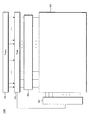
図1は実施の形態1のテレビジョン受信機100の要部構成を示す機能ブロック図である。
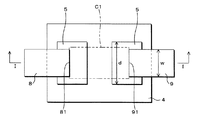
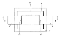
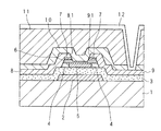
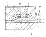
以後、チャネル領域(第1チャネル領域C1)を形成する工程が行われ、上述したように、第1チャネル領域C1内にポリシリコン層5の領域を選択的に形成する。
本発明は実施の形態1の記載に限るものでない。実施の形態2に係るテレビジョン受信機100においては、ピクセル薄膜トランジスタ(第1チャネル領域C1)の構成が実施の形態1とは異なるものの、実施の形態1と同様、斯かる第1チャネル領域C1及び斯かる第2チャネル領域C2は、電気的特性が相違するように構成されている。以下、詳しく説明する。
本発明は実施の形態1、2の記載に限るものでない。実施の形態3に係るテレビジョン受信機100においては、ピクセル薄膜トランジスタ(第1チャネル領域C1)の構成が実施の形態1、2とは異なるものの、実施の形態1、2と同様、斯かる第1チャネル領域C1及び斯かる第2チャネル領域C2は、電気的特性が相違するように構成されている。以下、詳しく説明する。
本発明は実施の形態1〜3の記載に限るものでない。実施の形態4に係るテレビジョン受信機100においては、ピクセル薄膜トランジスタ(第1チャネル領域C1)の構成が実施の形態1〜3とは異なるものの、実施の形態1〜3と同様、斯かる第1チャネル領域C1及び斯かる第2チャネル領域C2は、電気的特性が相違するように構成されている。以下、詳しく説明する。
本発明は実施の形態1〜4の記載に限るものでない。実施の形態5に係るテレビジョン受信機100においては、ピクセル薄膜トランジスタ(第1チャネル領域C1)の構成が実施の形態1〜4とは異なるものの、実施の形態1〜4と同様、斯かる第1チャネル領域C1及び斯かる第2チャネル領域C2は、電気的特性が相違するように構成されている。以下、詳しく説明する。
5 ポリシリコン層
8 ソース電極
9 ドレイン電極
81 端部
91 端部
100 テレビジョン受信機
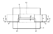
C1 第1チャネル領域
C2 第2チャネル領域
Claims (8)
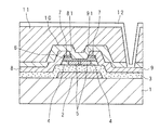
- 第1薄膜トランジスタを有する絵素と、第2薄膜トランジスタを有し、前記絵素を駆動する駆動回路とを備える表示装置において、
前記第1薄膜トランジスタおよび前記第2薄膜トランジスタは、それぞれ、ゲート電極と、前記ゲート電極を覆うゲート絶縁膜と、前記ゲート絶縁膜上に形成されている第1のアモルファスシリコン層と、前記第1のアモルファスシリコン層を覆う第2のアモルファスシリコン層と、前記第2のアモルファスシリコン層の上側に積層されていて所定の間隔を挟んで離隔されているソース電極およびドレイン電極と、を含み、
前記第1薄膜トランジスタは第1チャネル領域を有し、前記第2薄膜トランジスタは第2チャネル領域を有しており、
前記第1チャネル領域および前記第2チャネル領域は、前記第1のアモルファスシリコン層における上面視で前記ソース電極と前記ドレイン電極とに挟まれた領域を含み、
前記第1チャネル領域は前記第1のアモルファスシリコン層における上面視で前記ソース電極と前記ドレイン電極とに挟まれた領域においてアモルファスシリコン領域及びポリシリコン領域を含み、
前記第2チャネル領域は前記第1のアモルファスシリコン層における上面視で前記ソース電極と前記ドレイン電極とに挟まれた領域においてアモルファスシリコン領域を含まずにポリシリコン領域を含み、
前記第1チャネル領域及び前記第2チャネル領域は、電気的特性が相違することを特徴とする表示装置。 - 前記第1チャネル領域に含まれる第1ポリシリコン領域は離隔された2ヶ所であり、
一方の前記第1ポリシリコン領域は、前記積層の方向にて、前記ソース電極と重なっており、
他方の前記第1ポリシリコン領域は、前記積層の方向において、前記ドレイン電極と重なっていることを特徴とする請求項1に記載の表示装置。 - 前記第1チャネル領域に含まれる第1ポリシリコン領域は前記ソース電極及び前記ドレイン電極の離隔の方向に長く、
前記第1ポリシリコン領域の両端側が、前記積層の方向にて、前記ソース電極及び前記ドレイン電極の両対向端の一部と夫々重なっていることを特徴とする請求項1に記載の表示装置。 - 前記第1ポリシリコン領域は、前記ソース電極及び前記ドレイン電極の両対向端の中間にて、前記離隔の方向と直交する方向の寸法が大きくなることを特徴とする請求項3に記載の表示装置。
- 前記第1チャネル領域に含まれる第1ポリシリコン領域は1ヶ所であって、前記ソース電極及び前記ドレイン電極の両対向端の間に介在し、
前記積層の方向にて、前記ソース電極及び前記ドレイン電極の両対向端と重なっていないことを特徴とする請求項1に記載の表示装置。 - 前記第1チャネル領域に含まれる第1ポリシリコン領域と、前記第2チャネル領域に含まれる第2ポリシリコン領域とは、ポリシリコンの結晶性が異なることを特徴とする請求項1記載の表示装置。
- 第1薄膜トランジスタを有する複数の画素と、第2薄膜トランジスタを有し、該画素を駆動する駆動回路とを備える表示装置の製造方法において、
複数のゲート電極に係るゲート電極絶縁層を形成する工程と、
該ゲート電極絶縁層の上にアモルファスシリコン層を形成する工程と、
前記第1薄膜トランジスタに係る第1チャネル領域を形成するチャネル工程と、
ソース電極及びドレイン電極を形成する工程と、を含み、
前記チャネル工程では、前記アモルファスシリコン層における前記ゲート電極の上側であって上面視で前記ソース電極および前記ドレイン電極の間となるべき前記第1チャネル領域にポリシリコン領域が選択的に形成されることを特徴とする表示装置の製造方法。 - 前記チャネル工程では
前記アモルファスシリコン層にエネルギービームを部分的に照射してポリシリコン層に変化させるアニール工程と、
前記ポリシリコン層を覆って他のアモルファスシリコン層を形成する工程と、
前記他のアモルファスシリコン層の表面にn+シリコン層を形成する工程と
を含むことを特徴とする請求項7に記載の表示装置の製造方法。
Applications Claiming Priority (1)
| Application Number | Priority Date | Filing Date | Title |
|---|---|---|---|
| PCT/JP2015/075759 WO2017042941A1 (ja) | 2015-09-10 | 2015-09-10 | 表示装置及び表示装置の製造方法 |
Publications (2)
| Publication Number | Publication Date |
|---|---|
| JPWO2017042941A1 JPWO2017042941A1 (ja) | 2018-08-16 |
| JP6471237B2 true JP6471237B2 (ja) | 2019-02-13 |
Family
ID=58239348
Family Applications (1)
| Application Number | Title | Priority Date | Filing Date |
|---|---|---|---|
| JP2017538802A Expired - Fee Related JP6471237B2 (ja) | 2015-09-10 | 2015-09-10 | 表示装置及び表示装置の製造方法 |
Country Status (4)
| Country | Link |
|---|---|
| US (1) | US10310347B2 (ja) |
| JP (1) | JP6471237B2 (ja) |
| CN (1) | CN108028030A (ja) |
| WO (1) | WO2017042941A1 (ja) |
Families Citing this family (7)
| Publication number | Priority date | Publication date | Assignee | Title |
|---|---|---|---|---|
| US11726376B2 (en) * | 2016-11-23 | 2023-08-15 | Semiconductor Energy Laboratory Co., Ltd. | Display device, display module, and electronic device |
| JP2020004859A (ja) * | 2018-06-28 | 2020-01-09 | 堺ディスプレイプロダクト株式会社 | 薄膜トランジスタ、表示装置及び薄膜トランジスタの製造方法 |
| CN110137261A (zh) * | 2018-10-29 | 2019-08-16 | 京东方科技集团股份有限公司 | 薄膜晶体管及其制备方法、阵列基板和显示装置 |
| CN110071125A (zh) * | 2019-05-05 | 2019-07-30 | 京东方科技集团股份有限公司 | Tft背板及其制备方法、oled显示面板 |
| CN113593492B (zh) * | 2021-07-15 | 2022-10-04 | Tcl华星光电技术有限公司 | 显示面板的驱动系统及显示面板的驱动方法 |
| CN114023768A (zh) * | 2021-10-26 | 2022-02-08 | 惠州华星光电显示有限公司 | 阵列基板及其制备方法和显示面板 |
| CN116169179A (zh) * | 2022-12-12 | 2023-05-26 | 深超光电(深圳)有限公司 | 薄膜晶体管、薄膜晶体管阵列基板及薄膜晶体管制作方法 |
Family Cites Families (14)
| Publication number | Priority date | Publication date | Assignee | Title |
|---|---|---|---|---|
| JP2814319B2 (ja) * | 1991-08-29 | 1998-10-22 | 株式会社日立製作所 | 液晶表示装置及びその製造方法 |
| JPH05226656A (ja) * | 1992-02-13 | 1993-09-03 | Hitachi Ltd | 薄膜半導体装置及びその製造方法 |
| JPH0738110A (ja) * | 1993-07-21 | 1995-02-07 | Toshiba Corp | 半導体装置の製造方法 |
| JP3795606B2 (ja) * | 1996-12-30 | 2006-07-12 | 株式会社半導体エネルギー研究所 | 回路およびそれを用いた液晶表示装置 |
| JP2007027202A (ja) * | 2005-07-12 | 2007-02-01 | Sharp Corp | 表示装置の製造方法および表示装置 |
| JP2009099636A (ja) | 2007-10-15 | 2009-05-07 | Hitachi Displays Ltd | 表示装置および表示装置の製造方法 |
| KR101383705B1 (ko) * | 2007-12-18 | 2014-04-10 | 삼성디스플레이 주식회사 | 박막 트랜지스터, 박막 트랜지스터를 포함하는 표시 장치및 그 제조 방법 |
| KR101427585B1 (ko) * | 2008-01-04 | 2014-08-08 | 삼성디스플레이 주식회사 | 박막 트랜지스터, 박막 트랜지스터를 포함하는 표시 장치및 그 제조 방법 |
| KR101432716B1 (ko) * | 2008-02-25 | 2014-08-21 | 삼성디스플레이 주식회사 | 박막 트랜지스터, 박막 트랜지스터를 포함하는 표시 장치및 그 제조 방법 |
| JP5411528B2 (ja) * | 2008-03-18 | 2014-02-12 | 株式会社半導体エネルギー研究所 | 薄膜トランジスタ及び表示装置 |
| JP5004101B2 (ja) * | 2008-12-07 | 2012-08-22 | 栄 田中 | 高性能表示装置とその製造方法 |
| JP2010245480A (ja) * | 2009-04-10 | 2010-10-28 | Hitachi Displays Ltd | 表示装置 |
| JP2012114131A (ja) | 2010-11-22 | 2012-06-14 | Panasonic Corp | 薄膜トランジスタ、その製造方法、および表示装置 |
| JP2013161963A (ja) * | 2012-02-06 | 2013-08-19 | Panasonic Corp | 薄膜トランジスタ、薄膜トランジスタの製造方法、及び表示装置 |
-
2015
- 2015-09-10 CN CN201580083060.7A patent/CN108028030A/zh active Pending
- 2015-09-10 WO PCT/JP2015/075759 patent/WO2017042941A1/ja not_active Ceased
- 2015-09-10 JP JP2017538802A patent/JP6471237B2/ja not_active Expired - Fee Related
-
2018
- 2018-03-09 US US15/917,006 patent/US10310347B2/en active Active
Also Published As
| Publication number | Publication date |
|---|---|
| JPWO2017042941A1 (ja) | 2018-08-16 |
| CN108028030A (zh) | 2018-05-11 |
| WO2017042941A1 (ja) | 2017-03-16 |
| US10310347B2 (en) | 2019-06-04 |
| US20180196294A1 (en) | 2018-07-12 |
Similar Documents
| Publication | Publication Date | Title |
|---|---|---|
| JP6471237B2 (ja) | 表示装置及び表示装置の製造方法 | |
| CN107408578B (zh) | 薄膜晶体管以及显示面板 | |
| JP6334057B2 (ja) | 薄膜トランジスタ及び表示パネル | |
| JP6503458B2 (ja) | 薄膜トランジスタの製造方法及び表示パネル | |
| US20070045627A1 (en) | Thin film transistor substrate and method of manufacturing the same | |
| US10038098B2 (en) | Method for manufacturing thin film transistor, thin film transistor and display panel | |
| KR101250789B1 (ko) | 액정표시장치의 제조방법 | |
| JP2009099636A (ja) | 表示装置および表示装置の製造方法 | |
| WO2010050161A1 (ja) | 半導体装置およびその製造方法ならびに表示装置 | |
| WO2012004925A1 (ja) | 半導体装置及びその製造方法並びに液晶表示装置 | |
| US20100109010A1 (en) | Display device | |
| KR101250790B1 (ko) | 액정표시장치의 제조방법 | |
| WO2016104253A1 (ja) | 半導体装置 | |
| JP4669834B2 (ja) | 液晶表示装置の製造方法 | |
| JP2009076707A (ja) | 表示装置の製造方法 | |
| KR102092544B1 (ko) | 어레이 기판 및 이의 제조 방법 | |
| KR101250788B1 (ko) | 액정표시장치의 제조방법 | |
| JP2008047919A (ja) | 薄膜トランジスタ表示板の製造方法 | |
| JP2006317638A (ja) | 液晶表示装置の製造方法 | |
| WO2017168594A1 (ja) | 薄膜トランジスタ、表示パネル及び薄膜トランジスタの製造方法 | |
| JP2004273820A (ja) | 電極基板 | |
| KR20080077519A (ko) | 액정표시장치의 제조방법 |
Legal Events
| Date | Code | Title | Description |
|---|---|---|---|
| A521 | Request for written amendment filed |
Free format text: JAPANESE INTERMEDIATE CODE: A523 Effective date: 20180308 |
|
| A621 | Written request for application examination |
Free format text: JAPANESE INTERMEDIATE CODE: A621 Effective date: 20180308 |
|
| TRDD | Decision of grant or rejection written | ||
| A01 | Written decision to grant a patent or to grant a registration (utility model) |
Free format text: JAPANESE INTERMEDIATE CODE: A01 Effective date: 20181225 |
|
| A61 | First payment of annual fees (during grant procedure) |
Free format text: JAPANESE INTERMEDIATE CODE: A61 Effective date: 20190121 |
|
| R150 | Certificate of patent or registration of utility model |
Ref document number: 6471237 Country of ref document: JP Free format text: JAPANESE INTERMEDIATE CODE: R150 |
|
| LAPS | Cancellation because of no payment of annual fees |