JP6300662B2 - 半導体装置および半導体装置の製造方法 - Google Patents
半導体装置および半導体装置の製造方法 Download PDFInfo
- Publication number
- JP6300662B2 JP6300662B2 JP2014127439A JP2014127439A JP6300662B2 JP 6300662 B2 JP6300662 B2 JP 6300662B2 JP 2014127439 A JP2014127439 A JP 2014127439A JP 2014127439 A JP2014127439 A JP 2014127439A JP 6300662 B2 JP6300662 B2 JP 6300662B2
- Authority
- JP
- Japan
- Prior art keywords
- silicon substrate
- semiconductor device
- silicon
- layer
- substrate
- Prior art date
- Legal status (The legal status is an assumption and is not a legal conclusion. Google has not performed a legal analysis and makes no representation as to the accuracy of the status listed.)
- Expired - Fee Related
Links
Images


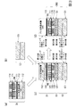

Classifications
-
- H—ELECTRICITY
- H10—SEMICONDUCTOR DEVICES; ELECTRIC SOLID-STATE DEVICES NOT OTHERWISE PROVIDED FOR
- H10F—INORGANIC SEMICONDUCTOR DEVICES SENSITIVE TO INFRARED RADIATION, LIGHT, ELECTROMAGNETIC RADIATION OF SHORTER WAVELENGTH OR CORPUSCULAR RADIATION
- H10F39/00—Integrated devices, or assemblies of multiple devices, comprising at least one element covered by group H10F30/00, e.g. radiation detectors comprising photodiode arrays
- H10F39/10—Integrated devices
- H10F39/12—Image sensors
- H10F39/18—Complementary metal-oxide-semiconductor [CMOS] image sensors; Photodiode array image sensors
-
- H—ELECTRICITY
- H10—SEMICONDUCTOR DEVICES; ELECTRIC SOLID-STATE DEVICES NOT OTHERWISE PROVIDED FOR
- H10F—INORGANIC SEMICONDUCTOR DEVICES SENSITIVE TO INFRARED RADIATION, LIGHT, ELECTROMAGNETIC RADIATION OF SHORTER WAVELENGTH OR CORPUSCULAR RADIATION
- H10F39/00—Integrated devices, or assemblies of multiple devices, comprising at least one element covered by group H10F30/00, e.g. radiation detectors comprising photodiode arrays
- H10F39/011—Manufacture or treatment of image sensors covered by group H10F39/12
- H10F39/018—Manufacture or treatment of image sensors covered by group H10F39/12 of hybrid image sensors
-
- H—ELECTRICITY
- H10—SEMICONDUCTOR DEVICES; ELECTRIC SOLID-STATE DEVICES NOT OTHERWISE PROVIDED FOR
- H10F—INORGANIC SEMICONDUCTOR DEVICES SENSITIVE TO INFRARED RADIATION, LIGHT, ELECTROMAGNETIC RADIATION OF SHORTER WAVELENGTH OR CORPUSCULAR RADIATION
- H10F39/00—Integrated devices, or assemblies of multiple devices, comprising at least one element covered by group H10F30/00, e.g. radiation detectors comprising photodiode arrays
- H10F39/10—Integrated devices
- H10F39/12—Image sensors
- H10F39/199—Back-illuminated image sensors
-
- H—ELECTRICITY
- H10—SEMICONDUCTOR DEVICES; ELECTRIC SOLID-STATE DEVICES NOT OTHERWISE PROVIDED FOR
- H10F—INORGANIC SEMICONDUCTOR DEVICES SENSITIVE TO INFRARED RADIATION, LIGHT, ELECTROMAGNETIC RADIATION OF SHORTER WAVELENGTH OR CORPUSCULAR RADIATION
- H10F39/00—Integrated devices, or assemblies of multiple devices, comprising at least one element covered by group H10F30/00, e.g. radiation detectors comprising photodiode arrays
- H10F39/80—Constructional details of image sensors
- H10F39/809—Constructional details of image sensors of hybrid image sensors
-
- H—ELECTRICITY
- H10—SEMICONDUCTOR DEVICES; ELECTRIC SOLID-STATE DEVICES NOT OTHERWISE PROVIDED FOR
- H10F—INORGANIC SEMICONDUCTOR DEVICES SENSITIVE TO INFRARED RADIATION, LIGHT, ELECTROMAGNETIC RADIATION OF SHORTER WAVELENGTH OR CORPUSCULAR RADIATION
- H10F39/00—Integrated devices, or assemblies of multiple devices, comprising at least one element covered by group H10F30/00, e.g. radiation detectors comprising photodiode arrays
- H10F39/80—Constructional details of image sensors
- H10F39/811—Interconnections
-
- H—ELECTRICITY
- H10—SEMICONDUCTOR DEVICES; ELECTRIC SOLID-STATE DEVICES NOT OTHERWISE PROVIDED FOR
- H10F—INORGANIC SEMICONDUCTOR DEVICES SENSITIVE TO INFRARED RADIATION, LIGHT, ELECTROMAGNETIC RADIATION OF SHORTER WAVELENGTH OR CORPUSCULAR RADIATION
- H10F99/00—Subject matter not provided for in other groups of this subclass
-
- H—ELECTRICITY
- H10—SEMICONDUCTOR DEVICES; ELECTRIC SOLID-STATE DEVICES NOT OTHERWISE PROVIDED FOR
- H10P—GENERIC PROCESSES OR APPARATUS FOR THE MANUFACTURE OR TREATMENT OF DEVICES COVERED BY CLASS H10
- H10P50/00—Etching of wafers, substrates or parts of devices
- H10P50/60—Wet etching
- H10P50/64—Wet etching of semiconductor materials
- H10P50/642—Chemical etching
- H10P50/644—Anisotropic liquid etching
-
- H—ELECTRICITY
- H10—SEMICONDUCTOR DEVICES; ELECTRIC SOLID-STATE DEVICES NOT OTHERWISE PROVIDED FOR
- H10P—GENERIC PROCESSES OR APPARATUS FOR THE MANUFACTURE OR TREATMENT OF DEVICES COVERED BY CLASS H10
- H10P50/00—Etching of wafers, substrates or parts of devices
- H10P50/69—Etching of wafers, substrates or parts of devices using masks for semiconductor materials
- H10P50/691—Etching of wafers, substrates or parts of devices using masks for semiconductor materials for Group IV materials or Group III-V materials
-
- H—ELECTRICITY
- H10—SEMICONDUCTOR DEVICES; ELECTRIC SOLID-STATE DEVICES NOT OTHERWISE PROVIDED FOR
- H10W—GENERIC PACKAGES, INTERCONNECTIONS, CONNECTORS OR OTHER CONSTRUCTIONAL DETAILS OF DEVICES COVERED BY CLASS H10
- H10W90/00—Package configurations
Landscapes
- Weting (AREA)
- Solid State Image Pick-Up Elements (AREA)
- Chemical & Material Sciences (AREA)
- Chemical Kinetics & Catalysis (AREA)
- General Chemical & Material Sciences (AREA)
- Engineering & Computer Science (AREA)
- Manufacturing & Machinery (AREA)
- Physics & Mathematics (AREA)
- Electromagnetism (AREA)
Priority Applications (3)
| Application Number | Priority Date | Filing Date | Title |
|---|---|---|---|
| JP2014127439A JP6300662B2 (ja) | 2014-06-20 | 2014-06-20 | 半導体装置および半導体装置の製造方法 |
| PCT/JP2015/061992 WO2015194249A1 (ja) | 2014-06-20 | 2015-04-20 | 半導体装置および半導体装置の製造方法 |
| US15/352,927 US9954027B2 (en) | 2014-06-20 | 2016-11-16 | Image pickup device and manufacturing method for image pickup device by stacking/bonding of crystalline silicon substrates |
Applications Claiming Priority (1)
| Application Number | Priority Date | Filing Date | Title |
|---|---|---|---|
| JP2014127439A JP6300662B2 (ja) | 2014-06-20 | 2014-06-20 | 半導体装置および半導体装置の製造方法 |
Publications (3)
| Publication Number | Publication Date |
|---|---|
| JP2016006840A JP2016006840A (ja) | 2016-01-14 |
| JP2016006840A5 JP2016006840A5 (enExample) | 2017-07-27 |
| JP6300662B2 true JP6300662B2 (ja) | 2018-03-28 |
Family
ID=54935246
Family Applications (1)
| Application Number | Title | Priority Date | Filing Date |
|---|---|---|---|
| JP2014127439A Expired - Fee Related JP6300662B2 (ja) | 2014-06-20 | 2014-06-20 | 半導体装置および半導体装置の製造方法 |
Country Status (3)
| Country | Link |
|---|---|
| US (1) | US9954027B2 (enExample) |
| JP (1) | JP6300662B2 (enExample) |
| WO (1) | WO2015194249A1 (enExample) |
Families Citing this family (3)
| Publication number | Priority date | Publication date | Assignee | Title |
|---|---|---|---|---|
| US12176348B2 (en) * | 2021-11-30 | 2024-12-24 | International Business Machines Corporation | Self-aligned hybrid substrate stacked gate-all-around transistors |
| US12660339B2 (en) | 2022-02-21 | 2026-06-16 | Taiwan Semiconductor Manufacturing Company, Ltd. | Stacked CMOS image sensor |
| JP2023178689A (ja) | 2022-06-06 | 2023-12-18 | キヤノン株式会社 | 光電変換装置、光電変換システム |
Family Cites Families (13)
| Publication number | Priority date | Publication date | Assignee | Title |
|---|---|---|---|---|
| JP2685819B2 (ja) | 1988-03-31 | 1997-12-03 | 株式会社東芝 | 誘電体分離半導体基板とその製造方法 |
| JPH07297377A (ja) * | 1994-04-21 | 1995-11-10 | Mitsubishi Electric Corp | 半導体装置およびその製造方法 |
| AU2003280857A1 (en) * | 2002-11-18 | 2004-06-15 | Hamamatsu Photonics K.K. | Backside-illuminated photodiode array, method for manufacturing same, and semiconductor device |
| US7810740B2 (en) | 2002-11-18 | 2010-10-12 | Hamamatsu Photonics K.K. | Back illuminated photodiode array, manufacturing method and semiconductor device thereof |
| JP2005053066A (ja) * | 2003-08-04 | 2005-03-03 | Seiko Epson Corp | ノズルプレートの製造方法、インクジェットヘッド及びインクジェット記録装置 |
| JP5577965B2 (ja) * | 2010-09-02 | 2014-08-27 | ソニー株式会社 | 半導体装置、および、その製造方法、電子機器 |
| JP5581954B2 (ja) * | 2010-10-07 | 2014-09-03 | ソニー株式会社 | 固体撮像装置、固体撮像装置の製造方法、及び電子機器 |
| JP2012094720A (ja) * | 2010-10-27 | 2012-05-17 | Sony Corp | 固体撮像装置、半導体装置、固体撮像装置の製造方法、半導体装置の製造方法、及び電子機器 |
| JP5665599B2 (ja) | 2011-02-24 | 2015-02-04 | 株式会社東芝 | 半導体装置および半導体装置の製造方法 |
| JP5853389B2 (ja) * | 2011-03-28 | 2016-02-09 | ソニー株式会社 | 半導体装置及び半導体装置の製造方法。 |
| JP5466338B2 (ja) * | 2011-03-31 | 2014-04-09 | 富士フイルム株式会社 | 固体撮像装置及び固体撮像装置の製造方法 |
| JP2013062382A (ja) | 2011-09-13 | 2013-04-04 | Toshiba Corp | 半導体装置およびその製造方法 |
| GB201121659D0 (en) * | 2011-12-16 | 2012-01-25 | Element Six Ltd | Substrates for semiconductor devices |
-
2014
- 2014-06-20 JP JP2014127439A patent/JP6300662B2/ja not_active Expired - Fee Related
-
2015
- 2015-04-20 WO PCT/JP2015/061992 patent/WO2015194249A1/ja not_active Ceased
-
2016
- 2016-11-16 US US15/352,927 patent/US9954027B2/en not_active Expired - Fee Related
Also Published As
| Publication number | Publication date |
|---|---|
| JP2016006840A (ja) | 2016-01-14 |
| US9954027B2 (en) | 2018-04-24 |
| WO2015194249A1 (ja) | 2015-12-23 |
| US20170062506A1 (en) | 2017-03-02 |
Similar Documents
| Publication | Publication Date | Title |
|---|---|---|
| KR102524686B1 (ko) | 반도체 장치, 및, 반도체 장치의 제조 방법 | |
| JP6335099B2 (ja) | 半導体装置および半導体装置の製造方法 | |
| CN102569328B (zh) | 感光成像装置、半导体器件的制作方法 | |
| TWI656657B (zh) | 太陽能電池模組中之太陽能電池之互連 | |
| CN102651379B (zh) | 半导体装置及半导体装置的制造方法 | |
| JP2009181981A (ja) | 半導体装置の製造方法および半導体装置 | |
| KR20160059738A (ko) | 프리패키지 및 이를 사용한 반도체 패키지의 제조 방법 | |
| CN107359210B (zh) | 用于制造光电转换设备的方法 | |
| US11276723B2 (en) | Semiconductor device, apparatus, and method for producing semiconductor device | |
| US9893116B2 (en) | Manufacturing method of electronic device and manufacturing method of semiconductor device | |
| TWI453905B (zh) | Manufacturing method of semiconductor device | |
| KR20150088633A (ko) | 적층형 이미지 센서 | |
| JP2013062382A (ja) | 半導体装置およびその製造方法 | |
| TW202301451A (zh) | 半導體裝置和製造半導體裝置的方法 | |
| JP5226228B2 (ja) | 半導体装置の製造方法、及び、半導体装置 | |
| JP2016006840A (ja) | 半導体装置および半導体装置の製造方法 | |
| JP2005322745A (ja) | 半導体素子、半導体素子の製造方法、固体撮像素子、並びに固体撮像素子の製造方法 | |
| US9312292B2 (en) | Back side illumination image sensor and manufacturing method thereof | |
| JP2009099875A (ja) | 半導体装置の製造方法 | |
| CN105453270A (zh) | 芯片驱动性能改善的背光图像传感器芯片 | |
| JP2015211090A (ja) | 半導体装置の製造方法 | |
| JP2016006840A5 (enExample) | ||
| CN102386198A (zh) | 制造光学传感器的方法 | |
| JP2023004854A (ja) | 半導体装置及びその製造方法 | |
| KR101439311B1 (ko) | 웨이퍼의 패드 형성 방법 |
Legal Events
| Date | Code | Title | Description |
|---|---|---|---|
| A521 | Request for written amendment filed |
Free format text: JAPANESE INTERMEDIATE CODE: A523 Effective date: 20170613 |
|
| A621 | Written request for application examination |
Free format text: JAPANESE INTERMEDIATE CODE: A621 Effective date: 20170613 |
|
| A521 | Request for written amendment filed |
Free format text: JAPANESE INTERMEDIATE CODE: A821 Effective date: 20170614 |
|
| A131 | Notification of reasons for refusal |
Free format text: JAPANESE INTERMEDIATE CODE: A131 Effective date: 20170912 |
|
| A521 | Request for written amendment filed |
Free format text: JAPANESE INTERMEDIATE CODE: A523 Effective date: 20171017 |
|
| A521 | Request for written amendment filed |
Free format text: JAPANESE INTERMEDIATE CODE: A821 Effective date: 20171018 |
|
| TRDD | Decision of grant or rejection written | ||
| A01 | Written decision to grant a patent or to grant a registration (utility model) |
Free format text: JAPANESE INTERMEDIATE CODE: A01 Effective date: 20180213 |
|
| A61 | First payment of annual fees (during grant procedure) |
Free format text: JAPANESE INTERMEDIATE CODE: A61 Effective date: 20180227 |
|
| R151 | Written notification of patent or utility model registration |
Ref document number: 6300662 Country of ref document: JP Free format text: JAPANESE INTERMEDIATE CODE: R151 |
|
| R250 | Receipt of annual fees |
Free format text: JAPANESE INTERMEDIATE CODE: R250 |
|
| R250 | Receipt of annual fees |
Free format text: JAPANESE INTERMEDIATE CODE: R250 |
|
| LAPS | Cancellation because of no payment of annual fees |