JP6300662B2 - Semiconductor device and manufacturing method of semiconductor device - Google Patents
Semiconductor device and manufacturing method of semiconductor device Download PDFInfo
- Publication number
- JP6300662B2 JP6300662B2 JP2014127439A JP2014127439A JP6300662B2 JP 6300662 B2 JP6300662 B2 JP 6300662B2 JP 2014127439 A JP2014127439 A JP 2014127439A JP 2014127439 A JP2014127439 A JP 2014127439A JP 6300662 B2 JP6300662 B2 JP 6300662B2
- Authority
- JP
- Japan
- Prior art keywords
- silicon substrate
- semiconductor device
- silicon
- layer
- substrate
- Prior art date
- Legal status (The legal status is an assumption and is not a legal conclusion. Google has not performed a legal analysis and makes no representation as to the accuracy of the status listed.)
- Expired - Fee Related
Links
- 239000004065 semiconductor Substances 0.000 title claims description 189
- 238000004519 manufacturing process Methods 0.000 title claims description 53
- XUIMIQQOPSSXEZ-UHFFFAOYSA-N Silicon Chemical compound [Si] XUIMIQQOPSSXEZ-UHFFFAOYSA-N 0.000 claims description 536
- 229910052710 silicon Inorganic materials 0.000 claims description 536
- 239000010703 silicon Substances 0.000 claims description 536
- 239000000758 substrate Substances 0.000 claims description 492
- 238000005530 etching Methods 0.000 claims description 106
- WGTYBPLFGIVFAS-UHFFFAOYSA-M tetramethylammonium hydroxide Chemical compound [OH-].C[N+](C)(C)C WGTYBPLFGIVFAS-UHFFFAOYSA-M 0.000 claims description 72
- 238000000034 method Methods 0.000 claims description 60
- 238000006243 chemical reaction Methods 0.000 claims description 19
- 239000011159 matrix material Substances 0.000 claims description 7
- 239000010410 layer Substances 0.000 description 180
- 238000003384 imaging method Methods 0.000 description 87
- 239000000243 solution Substances 0.000 description 66
- 238000001039 wet etching Methods 0.000 description 26
- KWYUFKZDYYNOTN-UHFFFAOYSA-M Potassium hydroxide Chemical compound [OH-].[K+] KWYUFKZDYYNOTN-UHFFFAOYSA-M 0.000 description 14
- 238000009792 diffusion process Methods 0.000 description 9
- 238000010030 laminating Methods 0.000 description 8
- 238000005286 illumination Methods 0.000 description 7
- 230000007547 defect Effects 0.000 description 6
- 239000011347 resin Substances 0.000 description 5
- 229920005989 resin Polymers 0.000 description 5
- KRHYYFGTRYWZRS-UHFFFAOYSA-N Fluorane Chemical compound F KRHYYFGTRYWZRS-UHFFFAOYSA-N 0.000 description 4
- 239000000853 adhesive Substances 0.000 description 4
- 230000001070 adhesive effect Effects 0.000 description 4
- 230000000694 effects Effects 0.000 description 4
- 238000010438 heat treatment Methods 0.000 description 4
- 239000012535 impurity Substances 0.000 description 4
- 230000001681 protective effect Effects 0.000 description 4
- 239000002356 single layer Substances 0.000 description 4
- 229910021421 monocrystalline silicon Inorganic materials 0.000 description 3
- 239000012212 insulator Substances 0.000 description 2
- 239000007788 liquid Substances 0.000 description 2
- 239000000126 substance Substances 0.000 description 2
- 239000012670 alkaline solution Substances 0.000 description 1
- 238000005520 cutting process Methods 0.000 description 1
- 230000002950 deficient Effects 0.000 description 1
- 238000003475 lamination Methods 0.000 description 1
- 239000000203 mixture Substances 0.000 description 1
- 238000012986 modification Methods 0.000 description 1
- 230000004048 modification Effects 0.000 description 1
- 238000007747 plating Methods 0.000 description 1
- 150000003376 silicon Chemical class 0.000 description 1
- 239000007787 solid Substances 0.000 description 1
- 238000007740 vapor deposition Methods 0.000 description 1
Images


Classifications
-
- H—ELECTRICITY
- H01—ELECTRIC ELEMENTS
- H01L—SEMICONDUCTOR DEVICES NOT COVERED BY CLASS H10
- H01L27/00—Devices consisting of a plurality of semiconductor or other solid-state components formed in or on a common substrate
- H01L27/14—Devices consisting of a plurality of semiconductor or other solid-state components formed in or on a common substrate including semiconductor components sensitive to infrared radiation, light, electromagnetic radiation of shorter wavelength or corpuscular radiation and specially adapted either for the conversion of the energy of such radiation into electrical energy or for the control of electrical energy by such radiation
- H01L27/144—Devices controlled by radiation
- H01L27/146—Imager structures
- H01L27/14643—Photodiode arrays; MOS imagers
-
- H—ELECTRICITY
- H01—ELECTRIC ELEMENTS
- H01L—SEMICONDUCTOR DEVICES NOT COVERED BY CLASS H10
- H01L21/00—Processes or apparatus adapted for the manufacture or treatment of semiconductor or solid state devices or of parts thereof
- H01L21/02—Manufacture or treatment of semiconductor devices or of parts thereof
- H01L21/04—Manufacture or treatment of semiconductor devices or of parts thereof the devices having at least one potential-jump barrier or surface barrier, e.g. PN junction, depletion layer or carrier concentration layer
- H01L21/18—Manufacture or treatment of semiconductor devices or of parts thereof the devices having at least one potential-jump barrier or surface barrier, e.g. PN junction, depletion layer or carrier concentration layer the devices having semiconductor bodies comprising elements of Group IV of the Periodic System or AIIIBV compounds with or without impurities, e.g. doping materials
- H01L21/30—Treatment of semiconductor bodies using processes or apparatus not provided for in groups H01L21/20 - H01L21/26
- H01L21/302—Treatment of semiconductor bodies using processes or apparatus not provided for in groups H01L21/20 - H01L21/26 to change their surface-physical characteristics or shape, e.g. etching, polishing, cutting
- H01L21/306—Chemical or electrical treatment, e.g. electrolytic etching
- H01L21/30604—Chemical etching
- H01L21/30608—Anisotropic liquid etching
-
- H—ELECTRICITY
- H01—ELECTRIC ELEMENTS
- H01L—SEMICONDUCTOR DEVICES NOT COVERED BY CLASS H10
- H01L21/00—Processes or apparatus adapted for the manufacture or treatment of semiconductor or solid state devices or of parts thereof
- H01L21/02—Manufacture or treatment of semiconductor devices or of parts thereof
- H01L21/04—Manufacture or treatment of semiconductor devices or of parts thereof the devices having at least one potential-jump barrier or surface barrier, e.g. PN junction, depletion layer or carrier concentration layer
- H01L21/18—Manufacture or treatment of semiconductor devices or of parts thereof the devices having at least one potential-jump barrier or surface barrier, e.g. PN junction, depletion layer or carrier concentration layer the devices having semiconductor bodies comprising elements of Group IV of the Periodic System or AIIIBV compounds with or without impurities, e.g. doping materials
- H01L21/30—Treatment of semiconductor bodies using processes or apparatus not provided for in groups H01L21/20 - H01L21/26
- H01L21/302—Treatment of semiconductor bodies using processes or apparatus not provided for in groups H01L21/20 - H01L21/26 to change their surface-physical characteristics or shape, e.g. etching, polishing, cutting
- H01L21/306—Chemical or electrical treatment, e.g. electrolytic etching
- H01L21/308—Chemical or electrical treatment, e.g. electrolytic etching using masks
-
- H—ELECTRICITY
- H01—ELECTRIC ELEMENTS
- H01L—SEMICONDUCTOR DEVICES NOT COVERED BY CLASS H10
- H01L25/00—Assemblies consisting of a plurality of individual semiconductor or other solid state devices ; Multistep manufacturing processes thereof
- H01L25/03—Assemblies consisting of a plurality of individual semiconductor or other solid state devices ; Multistep manufacturing processes thereof all the devices being of a type provided for in the same subgroup of groups H01L27/00 - H01L33/00, or in a single subclass of H10K, H10N, e.g. assemblies of rectifier diodes
- H01L25/04—Assemblies consisting of a plurality of individual semiconductor or other solid state devices ; Multistep manufacturing processes thereof all the devices being of a type provided for in the same subgroup of groups H01L27/00 - H01L33/00, or in a single subclass of H10K, H10N, e.g. assemblies of rectifier diodes the devices not having separate containers
- H01L25/065—Assemblies consisting of a plurality of individual semiconductor or other solid state devices ; Multistep manufacturing processes thereof all the devices being of a type provided for in the same subgroup of groups H01L27/00 - H01L33/00, or in a single subclass of H10K, H10N, e.g. assemblies of rectifier diodes the devices not having separate containers the devices being of a type provided for in group H01L27/00
- H01L25/0657—Stacked arrangements of devices
-
- H—ELECTRICITY
- H01—ELECTRIC ELEMENTS
- H01L—SEMICONDUCTOR DEVICES NOT COVERED BY CLASS H10
- H01L25/00—Assemblies consisting of a plurality of individual semiconductor or other solid state devices ; Multistep manufacturing processes thereof
- H01L25/16—Assemblies consisting of a plurality of individual semiconductor or other solid state devices ; Multistep manufacturing processes thereof the devices being of types provided for in two or more different main groups of groups H01L27/00 - H01L33/00, or in a single subclass of H10K, H10N, e.g. forming hybrid circuits
- H01L25/162—Assemblies consisting of a plurality of individual semiconductor or other solid state devices ; Multistep manufacturing processes thereof the devices being of types provided for in two or more different main groups of groups H01L27/00 - H01L33/00, or in a single subclass of H10K, H10N, e.g. forming hybrid circuits the devices being mounted on two or more different substrates
-
- H—ELECTRICITY
- H01—ELECTRIC ELEMENTS
- H01L—SEMICONDUCTOR DEVICES NOT COVERED BY CLASS H10
- H01L25/00—Assemblies consisting of a plurality of individual semiconductor or other solid state devices ; Multistep manufacturing processes thereof
- H01L25/16—Assemblies consisting of a plurality of individual semiconductor or other solid state devices ; Multistep manufacturing processes thereof the devices being of types provided for in two or more different main groups of groups H01L27/00 - H01L33/00, or in a single subclass of H10K, H10N, e.g. forming hybrid circuits
- H01L25/167—Assemblies consisting of a plurality of individual semiconductor or other solid state devices ; Multistep manufacturing processes thereof the devices being of types provided for in two or more different main groups of groups H01L27/00 - H01L33/00, or in a single subclass of H10K, H10N, e.g. forming hybrid circuits comprising optoelectronic devices, e.g. LED, photodiodes
-
- H—ELECTRICITY
- H01—ELECTRIC ELEMENTS
- H01L—SEMICONDUCTOR DEVICES NOT COVERED BY CLASS H10
- H01L25/00—Assemblies consisting of a plurality of individual semiconductor or other solid state devices ; Multistep manufacturing processes thereof
- H01L25/50—Multistep manufacturing processes of assemblies consisting of devices, each device being of a type provided for in group H01L27/00 or H01L29/00
-
- H—ELECTRICITY
- H01—ELECTRIC ELEMENTS
- H01L—SEMICONDUCTOR DEVICES NOT COVERED BY CLASS H10
- H01L27/00—Devices consisting of a plurality of semiconductor or other solid-state components formed in or on a common substrate
- H01L27/14—Devices consisting of a plurality of semiconductor or other solid-state components formed in or on a common substrate including semiconductor components sensitive to infrared radiation, light, electromagnetic radiation of shorter wavelength or corpuscular radiation and specially adapted either for the conversion of the energy of such radiation into electrical energy or for the control of electrical energy by such radiation
- H01L27/144—Devices controlled by radiation
- H01L27/146—Imager structures
- H01L27/14601—Structural or functional details thereof
- H01L27/14634—Assemblies, i.e. Hybrid structures
-
- H—ELECTRICITY
- H01—ELECTRIC ELEMENTS
- H01L—SEMICONDUCTOR DEVICES NOT COVERED BY CLASS H10
- H01L27/00—Devices consisting of a plurality of semiconductor or other solid-state components formed in or on a common substrate
- H01L27/14—Devices consisting of a plurality of semiconductor or other solid-state components formed in or on a common substrate including semiconductor components sensitive to infrared radiation, light, electromagnetic radiation of shorter wavelength or corpuscular radiation and specially adapted either for the conversion of the energy of such radiation into electrical energy or for the control of electrical energy by such radiation
- H01L27/144—Devices controlled by radiation
- H01L27/146—Imager structures
- H01L27/14601—Structural or functional details thereof
- H01L27/14636—Interconnect structures
-
- H—ELECTRICITY
- H01—ELECTRIC ELEMENTS
- H01L—SEMICONDUCTOR DEVICES NOT COVERED BY CLASS H10
- H01L27/00—Devices consisting of a plurality of semiconductor or other solid-state components formed in or on a common substrate
- H01L27/14—Devices consisting of a plurality of semiconductor or other solid-state components formed in or on a common substrate including semiconductor components sensitive to infrared radiation, light, electromagnetic radiation of shorter wavelength or corpuscular radiation and specially adapted either for the conversion of the energy of such radiation into electrical energy or for the control of electrical energy by such radiation
- H01L27/144—Devices controlled by radiation
- H01L27/146—Imager structures
- H01L27/14601—Structural or functional details thereof
- H01L27/1464—Back illuminated imager structures
-
- H—ELECTRICITY
- H01—ELECTRIC ELEMENTS
- H01L—SEMICONDUCTOR DEVICES NOT COVERED BY CLASS H10
- H01L27/00—Devices consisting of a plurality of semiconductor or other solid-state components formed in or on a common substrate
- H01L27/14—Devices consisting of a plurality of semiconductor or other solid-state components formed in or on a common substrate including semiconductor components sensitive to infrared radiation, light, electromagnetic radiation of shorter wavelength or corpuscular radiation and specially adapted either for the conversion of the energy of such radiation into electrical energy or for the control of electrical energy by such radiation
- H01L27/144—Devices controlled by radiation
- H01L27/146—Imager structures
- H01L27/14683—Processes or apparatus peculiar to the manufacture or treatment of these devices or parts thereof
- H01L27/1469—Assemblies, i.e. hybrid integration
Description
本発明は、半導体装置および半導体装置の製造方法に関する。 The present invention relates to a semiconductor device and a method for manufacturing the semiconductor device.
複数の半導体基板(シリコン基板)を積層した構造の半導体装置がある。また、半導体装置では、積層したシリコン基板の一方の面のシリコンをエッチングして薄化することも行われる。このような構造の半導体装置としては、例えば、裏面照射(BackSide Illumination:BSI)型の固体撮像装置がある。 There is a semiconductor device having a structure in which a plurality of semiconductor substrates (silicon substrates) are stacked. In the semiconductor device, silicon on one surface of the laminated silicon substrate is etched and thinned. As a semiconductor device having such a structure, for example, there is a backside illumination (BSI) type solid-state imaging device.
裏面照射(BackSide Illumination:BSI)型の固体撮像装置では、入射した光を光電変換する光電変換部などの回路要素が形成された面(表面)と反対側の面(裏面)から光を入射させる。このため、裏面照射型の固体撮像装置では、シリコン基板の裏面側の余分なシリコンをエッチングして薄化することによって、シリコン基板の表面側に形成された光電変換部により多くの光を入射させるようにする。 In a backside illumination (BSI) type solid-state imaging device, light is incident from a surface (back surface) opposite to a surface (front surface) on which circuit elements such as a photoelectric conversion unit that photoelectrically converts incident light are formed. . For this reason, in the backside illumination type solid-state imaging device, excess silicon on the back side of the silicon substrate is etched and thinned so that more light is incident on the photoelectric conversion unit formed on the front side of the silicon substrate. Like that.
しかし、シリコン基板を単に薄化すると、薄化したシリコン基板自体がロール状に巻かれてしまったり、割れてしまったりする。このため、裏面照射型の固体撮像装置など、積層したシリコン基板の一方の面のシリコンをエッチングして薄化する半導体装置では、薄化するシリコン基板を別のシリコン基板で支える(支持する)構成がとられる。 However, if the silicon substrate is simply thinned, the thinned silicon substrate itself is wound into a roll or cracked. For this reason, in a semiconductor device that etches and thins silicon on one surface of a stacked silicon substrate, such as a back-illuminated solid-state imaging device, the thinned silicon substrate is supported (supported) by another silicon substrate. Is taken.
例えば、裏面照射型の固体撮像装置では、光電変換部などの回路要素が形成されたシリコン基板(以下、「第1のシリコン基板」という)とは別のシリコン基板(以下、「第2のシリコン基板」という)を積層することによって、薄化する第1のシリコン基板を、第2のシリコン基板で支える(支持する)。このとき、裏面照射型の固体撮像装置では、第1のシリコン基板の表面側に第2のシリコン基板を積層した後に、第1のシリコン基板の裏面側の余分なシリコンをエッチングすることによって、第1のシリコン基板のみを薄化する。 For example, in a back-illuminated solid-state imaging device, a silicon substrate (hereinafter referred to as “second silicon”) different from a silicon substrate (hereinafter referred to as “first silicon substrate”) on which circuit elements such as a photoelectric conversion unit are formed. The first silicon substrate to be thinned is supported (supported) by the second silicon substrate. At this time, in the backside illumination type solid-state imaging device, the second silicon substrate is laminated on the front surface side of the first silicon substrate, and then the excess silicon on the back surface side of the first silicon substrate is etched, thereby Only one silicon substrate is thinned.
近年の半導体製造のプロセスでは、複数のシリコン基板を積層した構成の半導体装置に対して、一方のシリコン基板の余分なシリコンを除去して薄化するためのいくつかのエッチング方法が実用化されている。そして、複数のシリコン基板を積層した構成の半導体装置に対して、一方のシリコン基板の余分なシリコンを除去して薄化するエッチング方法としては、ウエットエッチング法が広く用いられている。 In recent semiconductor manufacturing processes, several etching methods for removing and thinning excess silicon from one silicon substrate have been put into practical use for semiconductor devices having a structure in which a plurality of silicon substrates are stacked. Yes. A wet etching method is widely used as an etching method for removing and thinning excess silicon from one silicon substrate in a semiconductor device having a structure in which a plurality of silicon substrates are stacked.
ウエットエッチング法は、特許文献1で示されたように、フッ硝酸、水酸化カリウム(potassium hydroxide,化学式=KOH)、または水酸化テトラメチルアンモニウム(TMAH:TetraMethylAmmonium Hydroxide)溶液など、異方性のエッチングを行うことができるアルカリ性のエッチング液によってシリコンをエッチングする方法である。このウエットエッチング法では、薄化したい半導体装置が複数形成されたウエハ基板を積層した状態で、アルカリ性のエッチング液に浸漬することによってシリコンをエッチングする。このため、積層したウエハ基板において露出しているシリコンが全てエッチングされてしまう。従って、ウエットエッチング法では、エッチングによって除去したくないシリコン、例えば、上述した裏面照射型の固体撮像装置においては、薄化する第1のシリコン基板を支える(支持する)第2のシリコン基板がエッチング液に晒されないように保護する必要がある。このエッチングによって除去したくないシリコンを保護する方法としては、シリコン基板を保護する保護膜として、熱処理などによって酸化膜を形成する方法などが用いられる。これは、アルカリ性のエッチング液が、酸化膜に対して高い選択性を示す、つまり、酸化膜をエッチングすることがないため、酸化膜がエッチング液に晒されたとしても、酸化膜が形成された側のシリコンがエッチングされてしまうことがないからである。 As shown in Patent Document 1, the wet etching method is an anisotropic etching such as hydrofluoric acid, potassium hydroxide (chemical formula = KOH), or tetramethylammonium hydroxide (TMAH) solution. This is a method of etching silicon with an alkaline etchant that can be used. In this wet etching method, silicon is etched by immersing it in an alkaline etching solution in a state where a plurality of semiconductor substrates to be thinned are stacked. For this reason, all the silicon exposed in the laminated wafer substrate is etched. Accordingly, in the wet etching method, silicon that is not to be removed by etching, for example, in the above-described back-illuminated solid-state imaging device, the second silicon substrate that supports (supports) the first silicon substrate to be thinned is etched. It is necessary to protect it from being exposed to the liquid. As a method for protecting silicon which is not desired to be removed by this etching, a method of forming an oxide film by heat treatment or the like is used as a protective film for protecting the silicon substrate. This is because the alkaline etching solution shows high selectivity with respect to the oxide film, that is, the oxide film is not etched, so that the oxide film was formed even when the oxide film was exposed to the etching solution. This is because the silicon on the side is not etched.
なお、薄化する第1のシリコン基板は、デバイス層とシリコン支持基板層とが埋め込み酸化膜(BOX:Buried Oxide)層によって貼り合わされて1枚のウエハ基板として構成されたSOI(Silicon On Insulator)構造のウエハ基板が用いられる。つまり、薄化する前の第1のシリコン基板は、デバイス層、BOX層、およびシリコン支持基板層の3層で構成されている。そして、SOI構造のウエハ基板には、デバイス層側に半導体装置の回路要素であるトランジスタや配線などが形成され、シリコン支持基板層が、エッチングによって除去される余分なシリコンとなる。例えば、上述した裏面照射型の固体撮像装置では、デバイス層に光電変換部などの回路要素が形成され、シリコン支持基板層がエッチングによって除去される。従って、ウエットエッチング法によってエッチングする場合には、第1のシリコン基板のデバイス層側の面に第2のシリコン基板を積層した後に、アルカリ性のエッチング液に浸漬することによって、シリコン支持基板層側からエッチングすることになる。このとき、デバイス層に形成された半導体装置の回路要素(例えば、裏面照射型の固体撮像装置における光電変換部など)は、上述した酸化膜によって除去したくないシリコンを保護する方法と同様に、酸化膜であるBOX層によって保護される。このように、薄化する第1のシリコン基板としてSOI構造のウエハ基板を用いることによって、SOI構造のウエハ基板のシリコン支持基板層のみを、ウエットエッチング法によってエッチングすることができる。 The first silicon substrate to be thinned is an SOI (Silicon On Insulator) configured as a single wafer substrate in which a device layer and a silicon support substrate layer are bonded together by a buried oxide (BOX) layer. A wafer substrate having a structure is used. That is, the first silicon substrate before thinning is composed of three layers: a device layer, a BOX layer, and a silicon support substrate layer. Then, on the wafer substrate having the SOI structure, transistors, wirings, and the like, which are circuit elements of the semiconductor device, are formed on the device layer side, and the silicon support substrate layer becomes extra silicon that is removed by etching. For example, in the above-described back-illuminated solid-state imaging device, circuit elements such as a photoelectric conversion unit are formed in the device layer, and the silicon support substrate layer is removed by etching. Therefore, in the case of etching by the wet etching method, the second silicon substrate is laminated on the surface of the first silicon substrate on the device layer side, and then immersed in an alkaline etching solution, so that the silicon support substrate layer side is exposed. Will be etched. At this time, the circuit element of the semiconductor device formed in the device layer (for example, the photoelectric conversion unit in the backside illumination type solid-state imaging device) is similar to the above-described method for protecting silicon that is not desired to be removed by the oxide film. It is protected by a BOX layer that is an oxide film. Thus, by using the SOI structure wafer substrate as the first silicon substrate to be thinned, only the silicon support substrate layer of the SOI structure wafer substrate can be etched by the wet etching method.
ウエットエッチング法では、エッチングによって除去したくないシリコンを保護するための保護膜として、酸化膜を形成する。この酸化膜は、半導体製造のプロセス、つまり、半導体装置が複数形成されたウエハ基板を製作する工程において、ウエットエッチング法によるエッチングを行う前に形成する。これにより、酸化膜に対して高い選択性を示す、つまり、酸化膜に対して高い選択比を持っているアルカリ性のエッチング液では、通常のウエットエッチング法によるエッチング工程において、酸化膜はほとんどエッチングされることはない。 In the wet etching method, an oxide film is formed as a protective film for protecting silicon that is not to be removed by etching. This oxide film is formed before performing etching by a wet etching method in a semiconductor manufacturing process, that is, a process of manufacturing a wafer substrate on which a plurality of semiconductor devices are formed. As a result, an alkaline etchant that exhibits high selectivity to the oxide film, that is, an alkaline etchant that has a high selectivity to the oxide film, is almost etched in the etching process by a normal wet etching method. Never happen.
しかしながら、第1のシリコン基板に積層する第2のシリコン基板において、シリコンの組成に欠陥がある箇所や異物が含まれている箇所では、エッチング工程の前に形成する酸化膜の形成状態が不均一になってしまう。つまり、第2のシリコン基板に形成した酸化膜に欠陥が生じてしまうことになる。このため、意図せずに酸化膜に欠陥が生じた箇所では、酸化膜に欠陥が生じていない箇所に比べて選択比が低下し、エッチング液によるエッチングの速度(エッチングレート)が速くなってしまうことがある。 However, in the second silicon substrate stacked on the first silicon substrate, the oxide film formed before the etching process is unevenly formed at a location where the silicon composition is defective or a location where foreign matter is included. Become. That is, a defect occurs in the oxide film formed on the second silicon substrate. For this reason, in a portion where an oxide film has a defect unintentionally, the selectivity is lower than that in a portion where the oxide film does not have a defect, and the etching rate (etching rate) by the etching solution increases. Sometimes.
また、半導体製造のプロセスでウエハ基板を製作する工程中にも、第2のシリコン基板に形成した酸化膜の表面に傷がついてしまうことがある。この酸化膜が傷ついた箇所においても、酸化膜に傷がついていない箇所に比べてエッチングレートが速くなってしまうことがある。 Also, the surface of the oxide film formed on the second silicon substrate may be damaged during the process of manufacturing the wafer substrate in the semiconductor manufacturing process. Even in a portion where the oxide film is damaged, the etching rate may be faster than a portion where the oxide film is not damaged.
この結果、アルカリ性のエッチング液によっても、保護膜として形成した酸化膜がエッチングされてしまい、保護しているはずのシリコンまでエッチング液が到達し、エッチングによって除去したくないシリコン、つまり、第2のシリコン基板までもエッチングされてしまう、という問題となる。 As a result, the oxide film formed as the protective film is also etched by the alkaline etching solution, and the etching solution reaches the silicon that should be protected. The problem is that even the silicon substrate is etched.
本発明は、上記の課題認識に基づいてなされたものであり、ウエットエッチング法によって所望の面のシリコンをエッチングした半導体装置およびこの半導体装置の製造方法を提供することを目的としている。 The present invention has been made based on recognition of the above problems, and an object of the present invention is to provide a semiconductor device in which silicon on a desired surface is etched by a wet etching method, and a method for manufacturing the semiconductor device.
上記の課題を解決するため、本発明の半導体装置は、薄化した第1のシリコン基板と、該第1のシリコン基板を支持する第2のシリコン基板とが積層される構造の半導体装置であって、当該半導体装置は、面方位が(100)または(110)の第1の面と、該第1の面の反対側の第2の面とを有する前記第1のシリコン基板と、第3の面と、該第3の面の反対側の面方位が(111)のシリコン面が露出した第4の面とを有する前記第2のシリコン基板とにおける前記第2の面と前記第3の面とを対向させて接合した後に、前記第1の面から前記第2の面に向けて予め定めた厚さのシリコンをエッチングして、前記第1のシリコン基板を薄化した、ことを特徴とする。 In order to solve the above problems, a semiconductor device of the present invention is a semiconductor device having a structure in which a thinned first silicon substrate and a second silicon substrate supporting the first silicon substrate are stacked. The semiconductor device includes a first silicon substrate having a first surface with a plane orientation of (100) or (110) and a second surface opposite to the first surface, and a third surface. The second surface and the third surface of the second silicon substrate having the surface of the second silicon substrate, and the fourth surface from which the silicon surface having the (111) orientation opposite to the third surface is exposed . The first silicon substrate is thinned by etching a predetermined thickness of silicon from the first surface toward the second surface after bonding with the surfaces facing each other. And
また、本発明の半導体装置は、前記第1のシリコン基板の前記第2の面側に形成され、入射する光に応じた電荷信号を発生する光電変換部を備えた画素を2次元の行列状に複数配置した画素部、を備えることを特徴とする。 According to another aspect of the present invention, there is provided a semiconductor device including a pixel including a photoelectric conversion unit that is formed on the second surface side of the first silicon substrate and generates a charge signal corresponding to incident light. And a plurality of pixel portions arranged in the same.
また、本発明の半導体装置は、前記第2のシリコン基板の前記第3の面側に形成され、前記画素部内のそれぞれの前記画素に備えた前記光電変換部が発生した前記電荷信号に基づいた画素信号に対して、予め定めた処理を行うための回路要素を備えた処理回路、を備えることを特徴とする。 Further, the semiconductor device of the present invention is based on the charge signal generated by the photoelectric conversion unit provided in each pixel in the pixel unit, which is formed on the third surface side of the second silicon substrate. A processing circuit including a circuit element for performing a predetermined process on the pixel signal is provided.
また、本発明の半導体装置は、前記第1のシリコン基板の前記第2の面側と、前記第2のシリコン基板の前記第3の面側とのそれぞれに形成され、前記画素部内の回路要素と前記処理回路内の対応する回路要素とを接続する接続部、を備えることを特徴とする。 The semiconductor device of the present invention is formed on each of the second surface side of the first silicon substrate and the third surface side of the second silicon substrate, and is a circuit element in the pixel portion. And a connection part that connects the corresponding circuit element in the processing circuit.
また、本発明の半導体装置は、前記第1のシリコン基板の前記第2の面と、該第2の面に対向する前記第2のシリコン基板の前記第3の面との間に配置され、前記第1のシリコン基板の前記第2の面と前記第2のシリコン基板の前記第3の面とを接合する接合層を形成する、ことを特徴とする。 Moreover, the semiconductor device of the present invention is disposed between the second surface of the first silicon substrate and the third surface of the second silicon substrate facing the second surface, A bonding layer for bonding the second surface of the first silicon substrate and the third surface of the second silicon substrate is formed.
また、本発明の半導体装置の製造方法は、薄化した第1のシリコン基板と、該第1のシリコン基板を支持する第2のシリコン基板とが積層される構造の半導体装置の製造方法であって、当該半導体装置の製造方法は、面方位が(100)または(110)の第1の面と、該第1の面の反対側の第2の面とを有する前記第1のシリコン基板と、第3の面と、該第3の面の反対側の面方位が(111)のシリコン面が露出した第4の面とを有する前記第2のシリコン基板とにおける前記第2の面と前記第3の面とを対向させて接合する第1の工程と、前記第1の面と前記第4の面とがエッチング液に晒されるように、前記第1の工程によって前記第1のシリコン基板と前記第2のシリコン基板とを接合した状態で、前記エッチング液に浸漬する第2の工程と、を含むことを特徴とする。 The method for manufacturing a semiconductor device of the present invention is a method for manufacturing a semiconductor device having a structure in which a thinned first silicon substrate and a second silicon substrate that supports the first silicon substrate are stacked. The method for manufacturing the semiconductor device includes the first silicon substrate having a first surface having a plane orientation of (100) or (110) and a second surface opposite to the first surface. The second surface in the second silicon substrate having a third surface and a fourth surface from which the silicon surface having a surface orientation opposite to the third surface of (111) is exposed; The first silicon substrate is formed by the first step so as to expose the first surface and the fourth surface to an etching solution so that the first surface is bonded to the third surface and facing the third surface. And the second silicon substrate bonded to each other and immersed in the etching solution Characterized in that it comprises between steps a.
また、本発明の半導体装置の製造方法における前記エッチング液は、水酸化テトラメチルアンモニウム溶液である、ことを特徴とする。 Further, the etching solution in the method for manufacturing a semiconductor device of the present invention is a tetramethylammonium hydroxide solution.
また、本発明の半導体装置の製造方法は、前記第1の工程の前に、前記第1のシリコン基板の前記第2の面側に、入射する光に応じた電荷信号を発生する光電変換部を備えた画素を2次元の行列状に複数配置した画素部を形成する第4の工程、を含むことを特徴とする。 In the semiconductor device manufacturing method of the present invention, a photoelectric conversion unit that generates a charge signal corresponding to incident light on the second surface side of the first silicon substrate before the first step. And a fourth step of forming a pixel portion in which a plurality of pixels having the above are arranged in a two-dimensional matrix.
また、本発明の半導体装置の製造方法は、前記第1の工程の前に、前記第2のシリコン基板の前記第3の面側に、前記画素部内のそれぞれの前記画素に備えた前記光電変換部が発生した前記電荷信号に基づいた画素信号に対して、予め定めた処理を行うための回路要素を備えた処理回路を形成する第5の工程、を含むことを特徴とする。 Further, in the method for manufacturing a semiconductor device according to the present invention, the photoelectric conversion provided for each pixel in the pixel portion on the third surface side of the second silicon substrate before the first step. And a fifth step of forming a processing circuit including a circuit element for performing a predetermined process on the pixel signal based on the charge signal generated by the unit.
また、本発明の半導体装置の製造方法は、前記第4の工程および前記第5の工程の後で、前記第1の工程の前に、前記第1のシリコン基板の前記第2の面側と、前記第2のシリコン基板の前記第3の面側とのそれぞれに、前記画素部内の回路要素と前記処理回路内の対応する回路要素とを接続する接続部を形成する第6の工程、を含むことを特徴とする。 The method for manufacturing a semiconductor device according to the present invention includes the second surface side of the first silicon substrate after the fourth step and the fifth step and before the first step. A sixth step of forming a connection portion for connecting a circuit element in the pixel portion and a corresponding circuit element in the processing circuit to each of the third surface side of the second silicon substrate; It is characterized by including.
本発明によれば、ウエットエッチング法によって所望の面のシリコンをエッチングした半導体装置およびこの半導体装置の製造方法を提供することができるという効果が得られる。 According to the present invention, it is possible to provide a semiconductor device in which silicon on a desired surface is etched by a wet etching method and a method for manufacturing the semiconductor device.
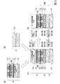
<第1の実施形態>
以下、本発明の実施形態について、図面を参照して説明する。図1は、本第1の実施形態による半導体装置の概略構造を示した断面図である。本第1の実施形態の半導体装置100は、2枚のシリコン基板(第1のシリコン基板11と第2のシリコン基板12)を積層することによって構成されている。なお、本第1の実施形態の半導体装置100は、ウエハ基板内に複数形成されるが、図1においては、説明を容易にするため、1つの半導体装置100が製造されるものとして説明する。
<First Embodiment>
Hereinafter, embodiments of the present invention will be described with reference to the drawings. FIG. 1 is a cross-sectional view showing a schematic structure of the semiconductor device according to the first embodiment. The
図1(a)には第1のシリコン基板11の構造、図1(b)には第2のシリコン基板12の構造、図1(c)には第1のシリコン基板11と第2のシリコン基板12とを積層した状態、図1(d)には半導体装置100の最終的な構造を示している。そして、図1では、図1(a)〜図1(d)によって、半導体装置100を製造する製造方法(製造工程)の概略を示している。
1A shows the structure of the
第1のシリコン基板11は、半導体装置100の機能(動作)を実現する回路要素が形成されたシリコン基板である。図1(a)に示したように、第1のシリコン基板11は、デバイス層111とシリコン支持基板層112とのそれぞれのシリコン層が、埋め込み酸化膜(BOX:Buried Oxide)層113(以下、「BOX層113」という)によって貼り合わされて1枚のウエハ基板として構成されたSOI(Silicon On Insulator)構造のウエハ基板に形成する。ここで、第1のシリコン基板11内のそれぞれのシリコン層、つまり、デバイス層111とシリコン支持基板層112とは、面方位が(100)である。この面方位が(100)のシリコン基板は、従来の半導体装置において多く用いられるシリコン基板である。
The
また、第1のシリコン基板11上のデバイス層111側には、拡散層や単層または複層の配線からなるトランジスタや配線などを、半導体装置100の機能(動作)を実現する回路要素として形成する。図1(a)には、トランジスタを形成するために第1のシリコン基板11上に形成した配線層114内の複層構成の配線を模式的に示している。また、図1(a)に示した第1のシリコン基板11の構造には、配線層114を形成する際に、熱処理などによって適宜形成する酸化膜115も示している。なお、図1(a)では、トランジスタを形成するためにデバイス層111内に形成する拡散層は省略している。
In addition, on the
第2のシリコン基板12は、第1のシリコン基板11をエッチングして薄化した際に、この第1のシリコン基板11を支える(支持する)単結晶のシリコン基板である。図1(b)に示したように、第2のシリコン基板12は、単層のシリコン層121で構成されたウエハ基板に形成する。ここで、第2のシリコン基板12のシリコン層121は、面方位が(111)である。この面方位(111)は、従来の半導体装置において多く用いられるシリコン基板の面方位(100)と異なる面方位である。
The
そして、半導体装置100は、第1のシリコン基板11と第2のシリコン基板12とを積層する。このとき、半導体装置100では、図1(c)に示したように、第1のシリコン基板11のシリコン支持基板層112側を第1の面とし、第1のシリコン基板11において回路要素を形成したデバイス層側を第2の面とする。また、第2のシリコン基板12の一方の面を第3の面とし、第2のシリコン基板12の他方の面を第4の面とする。そして、第1のシリコン基板11の第2の面と、第2のシリコン基板12の第3の面とを対向させ、接合層13によって第1のシリコン基板11と第2のシリコン基板12とを接合する。この接合層13は、第1のシリコン基板11と第2のシリコン基板12とを接合するための接着剤として、例えば、樹脂接着剤などの樹脂層131で形成する。
In the
そして、第1のシリコン基板11と第2のシリコン基板12とを積層(接合)した状態でエッチング液に浸漬することによって、第1のシリコン基板11の予め定めた厚さのシリコンをエッチングする。より具体的には、第1のシリコン基板11のシリコン支持基板層112をエッチングすることによって、最終的な構造の半導体装置100を製造する。つまり、図1(d)に示したように、積層した第1のシリコン基板11と第2のシリコン基板12との内、第1のシリコン基板11をウエットエッチング法によって薄化し、第1の面が第1Aの面となった最終的な構造の半導体装置100を製造する。
Then, the silicon of a predetermined thickness of the
なお、より正確には、第1のシリコン基板11と第2のシリコン基板12とが形成されたウエハ基板を積層(接合)した状態でエッチング液に浸漬することによって、第1のシリコン基板11が形成されたウエハ基板のシリコン支持基板層112をエッチングする。その後、エッチングした後の積層したウエハ基板からそれぞれの半導体装置100に切り分ける(ダイシングする)ことによって、最終的な構造の半導体装置100を製造する。
More precisely, the
このとき、ウエットエッチング法において用いるエッチング液としては、例えば、水酸化テトラメチルアンモニウム(TMAH:TetraMethylAmmonium Hydroxide)溶液(以下、「TMAH溶液」という)など、異方性のエッチングを行うことができるアルカリ性のエッチング液を用いる。以下の説明においては、ウエットエッチング法において用いるエッチング液として、TMAH溶液を用いるものとして説明する。 At this time, as an etchant used in the wet etching method, for example, an alkaline solution capable of performing anisotropic etching such as tetramethylammonium hydroxide (TMAH) solution (hereinafter referred to as “TMAH solution”) is used. Etching solution is used. In the following description, it is assumed that a TMAH solution is used as an etchant used in the wet etching method.
ここで、TMAH溶液によって第1のシリコン基板11のシリコン支持基板層112をエッチングすることができる理由を説明する。上述したように、第1のシリコン基板11のシリコン支持基板層112の面方位(100)であり、第2のシリコン基板12の面方位(111)である。つまり、図1(c)に示したようにそれぞれのシリコン基板を積層(接合)した状態では、第1の面の面方位が(100)、第4の面の面方位が(111)であり、それぞれの面で面方位が異なっている。そして、TMAH溶液は、異方性のエッチングを行うことができるエッチング液である。例えば、TMAH溶液におけるそれぞれの面方位に対してエッチングが進んでいく速度(エッチングレート)は、(100):(111)=20:1というように、エッチングレートに大きな差がある。
Here, the reason why the silicon
このため、TMAH溶液を用いてエッチングを行うと、面方位が(111)である第2のシリコン基板12よりも、面方位が(100)である第1のシリコン基板11のシリコン支持基板層112の方が、例えば、20倍多くエッチングされる。つまり、第4の面の第2のシリコン基板12がTMAH溶液に晒された場合でも、第2のシリコン基板12よりも、第1の面のシリコン支持基板層112の方がより多くエッチングされ、エッチングが進んでいっても、第2のシリコン基板12はほとんどエッチングされることはない。これにより、図1(c)に示したそれぞれのシリコン基板を積層(接合)した状態でTMAH溶液に浸漬すると、シリコン支持基板層112が、第1の面から第2の面の方向に向かって、順次エッチングされていく。
For this reason, when etching is performed using the TMAH solution, the silicon
なお、TMAH溶液によるエッチングが進み、シリコン支持基板層112の全てをエッチングした場合でも、第1のシリコン基板11上のデバイス層111側に形成された回路要素は、BOX層113によって保護される。これは、TMAH溶液の酸化膜に対する選択比が、例えば、シリコン:酸化膜=8000:1というように、選択性に非常に大きな差があるからである。このTMAH溶液における酸化膜に対する高い選択性によって、エッチングの進みが、BOX層113のところで停止するのと同様の状態になる。これにより、図1(d)に示したように、第1のシリコン基板11内のシリコン支持基板層112がエッチングされた構造の半導体装置100を製造することができる。
Even when the etching with the TMAH solution proceeds and all of the silicon
本第1の実施形態によれば、薄化した第1のシリコン基板(第1のシリコン基板11)と、この第1のシリコン基板11を支持する第2のシリコン基板(第2のシリコン基板12)とが積層される構造の半導体装置(半導体装置100)であって、この半導体装置100は、面方位が(100)または(110)の第1の面と、この第1の面の反対側の第2の面とを有する第1のシリコン基板11と、第3の面と、この第3の面の反対側の面方位が(111)の第4の面とを有する第2のシリコン基板12とにおける第2の面と第3の面とを対向させて接合した後に、第1の面から第2の面に向けて予め定めた厚さのシリコン(第1のシリコン基板11のシリコン支持基板層112)をエッチングして、第1のシリコン基板11を薄化した半導体装置100が構成される。
According to the first embodiment, the thinned first silicon substrate (first silicon substrate 11) and the second silicon substrate (second silicon substrate 12) that supports the
また、本第1の実施形態によれば、第1のシリコン基板11の第2の面と、この第2の面に対向する第2のシリコン基板12の第3の面との間に配置され、第1のシリコン基板11の第2の面と第2のシリコン基板12の第3の面とを接合する接合層(接合層13)を形成する半導体装置100が構成される。
In addition, according to the first embodiment, the
また、本第1の実施形態によれば、薄化した第1のシリコン基板11と、この第1のシリコン基板11を支持する第2のシリコン基板12とが積層される構造の半導体装置100の製造方法であって、この半導体装置100の製造方法は、面方位が(100)または(110)の第1の面と、この第1の面の反対側の第2の面とを有する第1のシリコン基板11と、第3の面と、この第3の面の反対側の面方位が(111)の第4の面とを有する第2のシリコン基板12とにおける第2の面と第3の面とを対向させて接合する第1の工程と、第1の面と第4の面とがエッチング液(アルカリ性のエッチング液:TMAH溶液)に晒されるように、第1の工程によって第1のシリコン基板11と第2のシリコン基板12とを接合した状態で、TMAH溶液に浸漬する第2の工程と、を含む半導体装置100の製造方法が構成される。
Moreover, according to the first embodiment, the
また、本第1の実施形態によれば、エッチング液は、水酸化テトラメチルアンモニウム溶液(アルカリ性のエッチング液:TMAH溶液)である半導体装置100の製造方法が構成される。
In addition, according to the first embodiment, the manufacturing method of the
上記に述べたように、本第1の実施形態の半導体装置100では、第1のシリコン基板11においてエッチングによって除去するシリコン支持基板層112の面方位と、エッチングによって除去したくない第2のシリコン基板12の面方位とを異なる面方位にする。そして、第1のシリコン基板11と第2のシリコン基板12とを積層した後に、異方性のエッチングを行うことができるアルカリ性のエッチング液によって、第1のシリコン基板11の予め定めた厚さのシリコンをウエットエッチングする。これにより、本第1の実施形態の半導体装置100では、ウエットエッチング法によって、所望の面のシリコン層、つまり、除去する対象のシリコン支持基板層112をエッチングすることができる。
As described above, in the
なお、本第1の実施形態の半導体装置100では、図1(特に、図1(b))を見てわかるように、第2のシリコン基板12を保護するための酸化膜を形成していない。つまり、本第1の実施形態の半導体装置100では、従来の半導体装置においてシリコン基板の一方の面をウエットエッチング法によってエッチングする際に、エッチングによって除去したくない面(保護する面)に形成していた酸化膜を形成していない。このため、本第1の実施形態の半導体装置100では、従来の半導体装置の製造においてエッチング工程前に必要であった、酸化膜を形成する工程を省略することができる。すなわち、本第1の実施形態の半導体装置100では、半導体装置100を製造する工程を少なくとも1工程少なくすることができる。これにより、本第1の実施形態の半導体装置100では、半導体装置100の製造におけるコストを削減することができる。また、第2のシリコン基板12に酸化膜を形成していないということは、従来の半導体装置を製造する際に必要であった、形成した酸化膜の表面の欠陥や傷に対する考慮も必要がなくなる。
In the
なお、本第1の実施形態の半導体装置100では、第2のシリコン基板12に酸化膜を形成していないため、TMAH溶液によって、第2のシリコン基板12も少しエッチングされることがある。この第2のシリコン基板12がエッチングされる量(厚さ)は、半導体装置100に大きな影響を与えるものではない。しかし、第2のシリコン基板12に酸化膜を形成することによって、TMAH溶液によって第2のシリコン基板12がよりエッチングされない構成にすることもできる。
In the
<第2の実施形態>
次に、第2の実施形態の半導体装置について説明する。本第2の実施形態の半導体装置は、第2のシリコン基板に酸化膜を形成することによって、ウエットエッチング法において用いるTMAH溶液における酸化膜に対する高い選択比を利用して、第2のシリコン基板の少ないエッチングも回避する構成である。図2は、本第2の実施形態による半導体装置の概略構造を示した断面図である。本第2の実施形態の半導体装置200も、図1に示した第1の実施形態の半導体装置100と同様に、2枚のシリコン基板(第1のシリコン基板11と第2のシリコン基板22)を積層することによって構成されている。また、本第2の実施形態の半導体装置200も、第1の実施形態の半導体装置100と同様に、ウエハ基板内に複数形成されるが、図2においても、説明を容易にするため、1つの半導体装置200が製造されるものとして説明する。
<Second Embodiment>
Next, the semiconductor device of the second embodiment will be described. In the semiconductor device according to the second embodiment, by forming an oxide film on the second silicon substrate, the high selectivity with respect to the oxide film in the TMAH solution used in the wet etching method is used. The structure avoids even a small amount of etching. FIG. 2 is a sectional view showing a schematic structure of the semiconductor device according to the second embodiment. Similarly to the
なお、本第2の実施形態の半導体装置200の構成は、第2のシリコン基板22に酸化膜を形成する以外は、図1に示した第1の実施形態の半導体装置100と同様の構成である。従って、以下の説明においては、本第2の実施形態の半導体装置200のそれぞれの構成において、第1の実施形態の半導体装置100と同様の構成には、第1の実施形態の半導体装置100と同一の符号を用いて説明し、第1の実施形態の半導体装置100と同様の構成に関する詳細な説明は省略する。
The configuration of the
図2(a)には第1のシリコン基板11の構造、図2(b)には第2のシリコン基板22の構造、図2(c)には第1のシリコン基板11と第2のシリコン基板22とを積層した状態、図2(d)には半導体装置200の最終的な構造を示している。そして、図2でも、図1と同様に、図2(a)〜図2(d)によって、半導体装置200を製造する製造方法(製造工程)の概略を示している。
2A shows the structure of the
図2(a)に示した第1のシリコン基板11は、第1の実施形態の半導体装置100と同様であるため、詳細な説明は省略する。
Since the
第2のシリコン基板22は、第1の実施形態の半導体装置100を構成する第2のシリコン基板12と同様に、第1のシリコン基板11をエッチングして薄化した際に、この第1のシリコン基板11を支える(支持する)単結晶のシリコン基板である。図2(b)に示したように、第2のシリコン基板22は、第1の実施形態の半導体装置100を構成する第2のシリコン基板12と同様の単層のシリコン層121で構成されたウエハ基板に形成する。ここで、第2のシリコン基板22のシリコン層121も、面方位が(111)である。
Similar to the
また、第2のシリコン基板22の両面は、熱処理などによって酸化膜(酸化膜222および酸化膜223)を形成する。これにより、第2のシリコン基板22は、ウエットエッチング法によってエッチングした場合でも、シリコン層121がTMAH溶液に晒されないように、酸化膜222および酸化膜223のそれぞれによって保護される。
Further, oxide films (
そして、半導体装置200は、第1の実施形態の半導体装置100と同様に、第1のシリコン基板11と第2のシリコン基板22とを積層する。このとき、半導体装置200では、図2(c)に示したように、第1のシリコン基板11のシリコン支持基板層112側を第1の面とし、第1のシリコン基板11において回路要素を形成したデバイス層側を第2の面とする。また、第2のシリコン基板22において酸化膜222が形成された面を第3の面とし、酸化膜223が形成された面を第4の面とする。そして、第1の実施形態の半導体装置100と同様に、第1のシリコン基板11の第2の面と、第2のシリコン基板22の第3の面とを対向させ、接合層13によって第1のシリコン基板11と第2のシリコン基板22とを接合する。なお、接合層13は、第1の実施形態の半導体装置100と同様であるため、詳細な説明は省略する。
And the
そして、第1の実施形態の半導体装置100と同様に、第1のシリコン基板11と第2のシリコン基板22とを積層(接合)した状態でTMAH溶液に浸漬することによって、第1のシリコン基板11の予め定めた厚さのシリコンをエッチングする。これにより、図2(d)に示したように、シリコン支持基板層112をエッチングして第1のシリコン基板11を薄化し、第1の面が第1Aの面となった最終的な構造の半導体装置200を製造する。
Then, similarly to the
このとき、半導体装置200では、第1の実施形態の半導体装置100と同様に、第1のシリコン基板11のシリコン支持基板層112の面方位と第2のシリコン基板22の面方位とが異なる構成に加えて、第2のシリコン基板22、特に、TMAH溶液に晒される第4の面側が酸化膜223によって保護されている。これは、上述したように、TMAH溶液の酸化膜に対する選択比が、例えば、シリコン:酸化膜=8000:1というように、選択性に非常に大きな差があるからである。この酸化膜に対する高い選択比によって、半導体装置200では、第4の面側がTMAH溶液によってエッチングされることがなく、図2(c)に示したそれぞれのシリコン基板が積層された状態において、シリコン支持基板層112が、第1の面から第2の面の方向に向かって、順次エッチングされていく。これにより、図2(d)に示したように、第1のシリコン基板11内のシリコン支持基板層112がエッチングされた構造の半導体装置200を製造することができる。
At this time, in the
本第2の実施形態によれば、少なくとも第2の工程の前に、第2のシリコン基板(第2のシリコン基板22)の少なくとも第4の面に酸化膜(酸化膜223)を形成する第3の工程、を含む半導体装置(半導体装置200)の製造方法が構成される。 According to the second embodiment, the oxide film (oxide film 223) is formed on at least the fourth surface of the second silicon substrate (second silicon substrate 22) at least before the second step. The manufacturing method of the semiconductor device (semiconductor device 200) including 3 processes is comprised.
上記に述べたように、本第2の実施形態の半導体装置200でも、第1の実施形態の半導体装置100と同様に、第1のシリコン基板11においてエッチングによって除去するシリコン支持基板層112の面方位と、エッチングによって除去したくない第2のシリコン基板22の面方位とを異なる面方位にする。また、本第2の実施形態の半導体装置200では、エッチングによって除去したくない第2のシリコン基板22を保護するための酸化膜を形成する。そして、第1の実施形態の半導体装置100と同様に、第1のシリコン基板11と第2のシリコン基板22とを積層した後に、異方性のエッチングを行うことができるアルカリ性のエッチング液によって、第1のシリコン基板11の予め定めた厚さのシリコンをウエットエッチングする。これにより、本第2の実施形態の半導体装置200では、ウエットエッチング法によって、所望の面のシリコン層、つまり、除去する対象のシリコン支持基板層112のみをエッチングすることができる。
As described above, also in the
なお、本第2の実施形態の半導体装置200では、第1の実施形態の半導体装置100のように酸化膜を形成する工程を省略することができない、すなわち、半導体装置200を製造する工程の数は、従来の半導体装置の製造と同様となる。しかし、本第2の実施形態の半導体装置200では、第1の実施形態の半導体装置100と同様のそれぞれのシリコン基板の面方位が異なる構成に加えて、第2のシリコン基板22においてTMAH溶液に晒される第4の面側を酸化膜223によって保護している。このため、本第2の実施形態の半導体装置200では、例え保護膜である酸化膜223の表面に欠陥や傷が生じていても、薄化した第1のシリコン基板11を支える(支持する)第2のシリコン基板22がエッチングされてしまう可能性を、従来の半導体装置よりも低くすることができる。
In the
また、本第2の実施形態の半導体装置200では、第2のシリコン基板22の両面に酸化膜(酸化膜222および酸化膜223)を形成している。そして、第1のシリコン基板11の配線層114は、この配線層114内に形成された複層構成の配線以外は、酸化膜である。このため、本第2の実施形態の半導体装置200においては、接合層13を形成せず、第1のシリコン基板11の第2の面の酸化膜と、第2のシリコン基板22の第3の面の酸化膜とを、酸化膜接合によって直接接合する構成にすることもできる。つまり、本第2の実施形態の半導体装置200において、第1のシリコン基板11における配線層114の酸化膜と、第2のシリコン基板22における酸化膜223とを、直接接合した構成にすることもできる。
In the
なお、本第2の実施形態の半導体装置200では、第2のシリコン基板22に酸化膜を形成した後に、第1のシリコン基板11と第2のシリコン基板22とを積層する場合について説明した。しかし、酸化膜223によって保護したい半導体装置200の面は、第4の面のみである。すなわち、第2のシリコン基板22は、半導体装置200の第4の面となる一方の面のみに酸化膜223が形成されていればよい。従って、本第2の実施形態の半導体装置200を製造する方法は、図2に示した方法に限定されるものではない。例えば、本第2の実施形態の半導体装置200を製造する方法として、第2のシリコン基板22の第4の面に相当する一方の面のみに酸化膜223を形成し、酸化膜223を形成していない第2のシリコン基板22の第3の面に相当する他方の面と、第1のシリコン基板11の第2の面とを対向させて積層する方法にすることもできる。また、例えば、本第2の実施形態の半導体装置200を製造する方法として、第1のシリコン基板11と第2のシリコン基板22とを積層した後に、半導体装置200の第4の面側のみに酸化膜223を形成する方法にすることもできる。
In the
<第3の実施形態>
次に、第3の実施形態の半導体装置について説明する。本第3の実施形態の半導体装置は、第1のシリコン基板に、入射する光に応じた電荷信号を発生するフォトダイオードなどの光電変換部を備えた画素を2次元の行列状に複数配置した画素部を形成した裏面照射型の固体撮像装置の構成である。図3は、本第3の実施形態による半導体装置(裏面照射型の固体撮像装置)の概略構造を示した断面図である。本第3の実施形態の半導体装置300(以下、「固体撮像装置300」という)も、図1に示した第1の実施形態の半導体装置100と同様に、2枚のシリコン基板(第1のシリコン基板31と第2のシリコン基板12)を積層することによって構成されている。また、本第3の実施形態の固体撮像装置300も、第1の実施形態の半導体装置100と同様に、ウエハ基板内に複数形成されるが、図3においても、説明を容易にするため、1つの固体撮像装置300が製造されるものとして説明する。
<Third Embodiment>
Next, a semiconductor device according to a third embodiment will be described. In the semiconductor device of the third embodiment, a plurality of pixels each having a photoelectric conversion unit such as a photodiode that generates a charge signal corresponding to incident light is arranged in a two-dimensional matrix on a first silicon substrate. This is a configuration of a back-illuminated solid-state imaging device in which a pixel portion is formed. FIG. 3 is a sectional view showing a schematic structure of the semiconductor device (backside illumination type solid-state imaging device) according to the third embodiment. Similarly to the
なお、本第3の実施形態の固体撮像装置300の構成は、第1のシリコン基板31にフォトダイオードなどの光電変換部を形成する以外は、図1に示した第1の実施形態の半導体装置100と同様の構成である。従って、以下の説明においては、本第3の実施形態の固体撮像装置300のそれぞれの構成において、第1の実施形態の半導体装置100と同様の構成には、第1の実施形態の半導体装置100と同一の符号を用いて説明し、第1の実施形態の半導体装置100と同様の構成に関する詳細な説明は省略する。
The configuration of the solid-
図3(a)には第1のシリコン基板31の構造、図3(b)には第2のシリコン基板12の構造、図3(c)には第1のシリコン基板31と第2のシリコン基板12とを積層した状態、図3(d)には固体撮像装置300の最終的な構造を示している。そして、図3でも、図1と同様に、図3(a)〜図3(d)によって、固体撮像装置300を製造する製造方法(製造工程)の概略を示している。
3A shows the structure of the
第1のシリコン基板31は、固体撮像装置300の機能(動作)を実現する回路要素が形成されたシリコン基板である。図3(a)に示したように、第1のシリコン基板31は、第1の実施形態の第1のシリコン基板11と同様のSOI構造のウエハ基板に形成する。ここで、第1のシリコン基板31内のそれぞれのシリコン層、つまり、デバイス層111とシリコン支持基板層112とは、第1の実施形態の第1のシリコン基板11と同様に、面方位が(100)である。
The
また、第1のシリコン基板31上のデバイス層111側には、拡散層や単層または複層の配線からなるフォトダイオードPD、トランジスタ、配線などを、固体撮像装置300の機能(動作)を実現する回路要素として形成する。図3(a)には、フォトダイオードPDを形成するためにデバイス層111内に形成した拡散層と、フォトダイオードPDやトランジスタを形成するために第1のシリコン基板31上に形成した配線層114内の複層構成の配線とを模式的に示している。また、図3(a)に示した第1のシリコン基板31の構造には、配線層114を形成する際に適宜形成する酸化膜115も示している。
Further, on the
図3(b)に示した第2のシリコン基板12は、第1の実施形態の半導体装置100と同様であるため、詳細な説明は省略する。なお、第2のシリコン基板12のシリコン層121の面方位は(111)である。
Since the
そして、固体撮像装置300は、第1の実施形態の半導体装置100と同様に、第1のシリコン基板31と第2のシリコン基板12とを積層する。このとき、固体撮像装置300では、図3(c)に示したように、第1のシリコン基板31のシリコン支持基板層112側を第1の面とし、第1のシリコン基板31においてフォトダイオードPDなどの回路要素を形成したデバイス層側を第2の面とする。また、第2のシリコン基板12は、第1の実施形態の第2のシリコン基板12と同様に、一方の面を第3の面とし、他方の面を第4の面とする。そして、第1の実施形態の半導体装置100と同様に、第1のシリコン基板31の第2の面と、第2のシリコン基板12の第3の面とを対向させ、接合層13によって第1のシリコン基板31と第2のシリコン基板12とを接合する。なお、接合層13は、第1の実施形態の半導体装置100と同様であるため、詳細な説明は省略する。
The solid-
そして、第1の実施形態の半導体装置100と同様に、第1のシリコン基板31と第2のシリコン基板12とを積層(接合)した状態でTMAH溶液に浸漬することによって、第1のシリコン基板31の予め定めた厚さのシリコンをエッチングする。これにより、図3(d)に示したように、第1のシリコン基板31内のシリコン支持基板層112をウエットエッチング法によって薄化し、第1の面が第1Aの面となった最終的な構造の固体撮像装置300を製造する。
Then, similarly to the
このとき、固体撮像装置300では、第1の実施形態の半導体装置100と同様に、第1のシリコン基板31のシリコン支持基板層112の面方位と第2のシリコン基板12の面方位とが異なるため、第1の面のシリコン支持基板層112の方が、第2のシリコン基板12よりも多くエッチングされ、エッチングが進んでいっても、第2のシリコン基板12はほとんどエッチングされることはない。このため、図3(c)に示したそれぞれのシリコン基板を積層した状態から、シリコン支持基板層112が、第1の面から第2の面の方向に向かって、順次エッチングされていく。これにより、図3(d)に示したように、第1のシリコン基板31内のシリコン支持基板層112が、BOX層113までエッチングされた構造の固体撮像装置300を製造することができる。
At this time, in the solid-
本第3の実施形態によれば、第1のシリコン基板(第1のシリコン基板31)の第2の面側に形成され、入射する光に応じた電荷信号を発生する光電変換部(フォトダイオードPD)を備えた画素を2次元の行列状に複数配置した画素部を備える半導体装置(固体撮像装置300)が構成される。 According to the third embodiment, the photoelectric conversion unit (photodiode) that is formed on the second surface side of the first silicon substrate (first silicon substrate 31) and generates a charge signal according to incident light. A semiconductor device (solid-state imaging device 300) including a pixel portion in which a plurality of pixels including PD) are arranged in a two-dimensional matrix is configured.
また、本第3の実施形態によれば、第1の工程の前に、第1のシリコン基板31の第2の面側に、入射する光に応じた電荷信号を発生するフォトダイオードPDを備えた画素を2次元の行列状に複数配置した画素部を形成する第4の工程、を含む固体撮像装置300の製造方法が構成される。
Further, according to the third embodiment, the photodiode PD that generates the charge signal corresponding to the incident light is provided on the second surface side of the
上記に述べたように、本第3の実施形態の固体撮像装置300でも、第1の実施形態の半導体装置100と同様に、第1のシリコン基板31においてエッチングによって除去するシリコン支持基板層112の面方位と、エッチングによって除去したくない第2のシリコン基板12の面方位とを異なる面方位にする。そして、第1の実施形態の半導体装置100と同様に、第1のシリコン基板31と第2のシリコン基板12とを積層した後に、異方性のエッチングを行うことができるアルカリ性のエッチング液によって、第1のシリコン基板31の予め定めた厚さのシリコンをウエットエッチングする。これにより、本第3の実施形態の固体撮像装置300では、ウエットエッチング法によって、所望の面のシリコン層、つまり、除去する対象のシリコン支持基板層112のみをエッチングすることができる。そして、本第3の実施形態の固体撮像装置300でも、第1の実施形態の半導体装置100と同様の効果を得ることができる。
As described above, even in the solid-
なお、図3に示した本第3の実施形態の固体撮像装置300では、第1の実施形態の半導体装置100と同様の構成である場合について説明したが、本第3の実施形態の固体撮像装置300を製造する方法は、図3に示した方法に限定されるものではない。つまり、本第3の実施形態の固体撮像装置300を、図2に示した半導体装置200と同様に、第1のシリコン基板31を支える(支持する)第2のシリコン基板12を、酸化膜によってエッチングから保護する構成にすることもできる。
In the solid-
なお、本第3の実施形態の固体撮像装置300では、第2のシリコン基板12が、第1のシリコン基板31を支える(支持する)のみの構成であったが、第2のシリコン基板12に、拡散層や単層または複層の配線からなるトランジスタや配線などを形成することによって、固体撮像装置300の機能(動作)を実現する構成にすることもできる。
In the solid-
<第4の実施形態>
次に、第4の実施形態の半導体装置について説明する。本第4の実施形態の半導体装置も、第3の実施形態の固体撮像装置300と同様に、第1のシリコン基板にフォトダイオードなどの光電変換部を備えた画素が2次元の行列状に複数配置された画素部を形成した裏面照射型の固体撮像装置の構成である。そして、本第4の実施形態の半導体装置は、第2のシリコン基板にも、本第4の実施形態の半導体装置の機能(動作)を実現する回路要素が形成された構成である。図4は、本第4の実施形態による半導体装置(裏面照射型の固体撮像装置)の概略構造を示した断面図である。本第4の実施形態の半導体装置400(以下、「固体撮像装置400」という)も、図1に示した第1の実施形態の半導体装置100や図3に示した第3の実施形態の固体撮像装置300と同様に、2枚のシリコン基板(第1のシリコン基板41と第2のシリコン基板42)を積層することによって構成されている。また、本第4の実施形態の固体撮像装置400も、第1の実施形態の半導体装置100や第3の実施形態の固体撮像装置300と同様に、ウエハ基板内に複数形成されるが、図4においても、説明を容易にするため、1つの固体撮像装置400が製造されるものとして説明する。
<Fourth Embodiment>
Next, a semiconductor device according to a fourth embodiment will be described. Similarly to the solid-
なお、本第4の実施形態の固体撮像装置400の構成には、第1の実施形態の半導体装置100や第3の実施形態の固体撮像装置300と同様の構成も含まれている。従って、以下の説明においては、本第4の実施形態の固体撮像装置400のそれぞれの構成において、第1の実施形態の半導体装置100や第3の実施形態の固体撮像装置300と同様の構成は、第1の実施形態の半導体装置100や第3の実施形態の固体撮像装置300と同一の符号を用いて詳細な説明は省略する。
Note that the configuration of the solid-
図4(a)および図4(b)には第1のシリコン基板41の構造、図4(c)および図4(d)には第2のシリコン基板42の構造、図4(e)には第1のシリコン基板41と第2のシリコン基板42とを積層した状態、図4(f)には固体撮像装置400の最終的な構造を示している。そして、図4でも、図3と同様に、図4(a)〜図4(f)によって、固体撮像装置400を製造する製造方法(製造工程)の概略を示している。
4 (a) and 4 (b) show the structure of the
第1のシリコン基板41は、第3の実施形態の固体撮像装置300と同様に、SOI構造のウエハ基板に固体撮像装置400の機能(動作)を実現する回路要素を形成するシリコン基板である。なお、第1のシリコン基板41内のそれぞれのシリコン層、つまり、デバイス層111とシリコン支持基板層112とは、第3の実施形態の固体撮像装置300と同様に、面方位が(100)である。
Similar to the solid-
また、第1のシリコン基板41上のデバイス層111側には、第3の実施形態の固体撮像装置300と同様に、フォトダイオードPD、トランジスタ、配線などを、固体撮像装置400の機能(動作)を実現する回路要素として形成する。図4(a)には、フォトダイオードPDを形成するためにデバイス層111内に形成した拡散層と、第1のシリコン基板41上に形成した配線層114内の複層構成の配線と、適宜形成する酸化膜115とを示している。
Further, on the
また、固体撮像装置400は、第1のシリコン基板41に積層する第2のシリコン基板42にも、固体撮像装置400の機能(動作)を実現する回路要素を形成する。このため、第1のシリコン基板41には、第2のシリコン基板42と電気的に接続するための接続部を形成する。図4(b)には、第1のシリコン基板41と第2のシリコン基板42とにおいて対応する回路要素同士を電気的に接続するために、配線層114上に形成した接続電極416を示している。なお、接続電極416は、例えば、蒸着法、めっき法で作製されるマイクロバンプなどである。
The solid-
第2のシリコン基板42は、第3の実施形態の固体撮像装置300と同様に、薄化した第1のシリコン基板41を支える(支持する)単結晶のシリコン基板である。なお、第2のシリコン基板42のシリコン層121の面方位は(111)である。
The
ただし、固体撮像装置400では、第2のシリコン基板42にも、固体撮像装置400の機能(動作)を実現する回路要素を形成する。この第2のシリコン基板42に形成する回路要素は、例えば、第1のシリコン基板41に形成されたフォトダイオードPDが発生した入射光に応じた電荷信号に基づいた画素信号に対して、予め定めた処理を行うための処理回路などとして構成される。このため、第2のシリコン基板42の一方の側には、拡散層や単層または複層の配線からなるトランジスタTrや配線などを、固体撮像装置400の機能(動作)を実現する回路要素として形成する。図4(c)には、トランジスタTrを形成するためにシリコン層121内に形成した拡散層と、トランジスタTrを形成するために第2のシリコン基板42上に形成した配線層422内の複層構成の配線とを模式的に示している。また、図4(c)に示した第2のシリコン基板42の構造には、配線層422を形成する際に、熱処理などによって適宜形成する酸化膜423も示している。
However, in the solid-
また、固体撮像装置400では、第2のシリコン基板42に形成された回路要素が、第1のシリコン基板41に形成された回路要素と電気的に接続されるため、第2のシリコン基板42にも、第1のシリコン基板41と電気的に接続するための接続部を形成する。図4(d)には、第1のシリコン基板41と第2のシリコン基板42とにおいて対応する回路要素同士を電気的に接続するために、配線層422上に形成した接続パット424を示している。この接続パット424は、第1のシリコン基板41の配線層114上に形成された接続電極416のそれぞれに対応する。
In the solid-
そして、固体撮像装置400は、第3の実施形態の固体撮像装置300と同様に、第1のシリコン基板41と第2のシリコン基板42とを積層する。このとき、固体撮像装置400では、図4(e)に示したように、第1のシリコン基板41のシリコン支持基板層112側を第1の面とし、第1のシリコン基板41において接続電極416を形成したデバイス層側を第2の面とする。また、第2のシリコン基板42は、第1のシリコン基板41に形成した回路要素と電気的接続される回路要素を形成した一方の側を第3の面とし、回路要素を形成していない他方の側を第4の面とする。そして、第3の実施形態の固体撮像装置300と同様に、第1のシリコン基板41の第2の面と、第2のシリコン基板42の第3の面とを対向させ、接合層43において、第1のシリコン基板41に形成された接続電極416と、第2のシリコン基板42に形成された接続パット424とを接続する接続電極層431を形成する。これにより、第1のシリコン基板41に形成された回路要素と、第2のシリコン基板42に形成された回路要素とが電気的に接続され、接続されたそれぞれのシリコン基板に形成された回路要素同士は、接続電極層431を介して信号の送受信を行う。
And the solid-
なお、接続電極層431は、第1のシリコン基板41と第2のシリコン基板42との間に存在する空間に、例えば、樹脂接着剤などの絶縁部材を充填してもよい。
In addition, the
そして、第3の実施形態の固体撮像装置300と同様に、第1のシリコン基板41と第2のシリコン基板42とを積層(接合)した状態でTMAH溶液に浸漬することによって、第1のシリコン基板41の予め定めた厚さのシリコンをエッチングする。これにより、図4(d)に示したように、第1のシリコン基板41内のシリコン支持基板層112をエッチングして第1のシリコン基板41を薄化し、第1の面が第1Aの面となった最終的な構造の固体撮像装置400を製造する。
Then, similarly to the solid-
このとき、固体撮像装置400では、第3の実施形態の固体撮像装置300と同様に、第1のシリコン基板41のシリコン支持基板層112の面方位と第2のシリコン基板42の面方位とが異なるため、第1の面のシリコン支持基板層112の方が、第2のシリコン基板42よりも多くエッチングされ、エッチングが進んでいっても、第2のシリコン基板42はほとんどエッチングされることはない。このため、図4(c)に示したそれぞれのシリコン基板を積層した状態から、シリコン支持基板層112が、第1の面から第2の面の方向に向かって、順次エッチングされていく。これにより、図4(d)に示したように、第1のシリコン基板41内のシリコン支持基板層112が、BOX層113までエッチングされた構造の固体撮像装置400を製造することができる。
At this time, in the solid-
本第4の実施形態によれば、第2のシリコン基板(第2のシリコン基板42)の第3の面側に形成され、画素部(第1のシリコン基板41の第2の面側に形成された画素部)内のそれぞれの画素に備えた光電変換部(フォトダイオードPD)が発生した電荷信号に基づいた画素信号に対して、予め定めた処理を行うための回路要素を備えた処理回路を備える半導体装置(固体撮像装置400)が構成される。 According to the fourth embodiment, it is formed on the third surface side of the second silicon substrate (second silicon substrate 42) and formed on the pixel surface (second surface side of the first silicon substrate 41). Processing circuit having a circuit element for performing a predetermined process on a pixel signal based on a charge signal generated by a photoelectric conversion unit (photodiode PD) included in each pixel in the pixel) The semiconductor device (solid-state imaging device 400) provided with is comprised.
また、本第4の実施形態によれば、第1のシリコン基板(第1のシリコン基板41)の第2の面側と、第2のシリコン基板42の第3の面側とのそれぞれに形成され、画素部(第1のシリコン基板41の第2の面側に形成された画素部)内の回路要素と処理回路(第2のシリコン基板42の第3の面側に形成された処理回路)内の対応する回路要素とを接続する接続部(接続電極416および接続パット424)を備える固体撮像装置400が構成される。
Further, according to the fourth embodiment, the first silicon substrate (first silicon substrate 41) is formed on each of the second surface side and the second surface side of the
また、本第4の実施形態によれば、第1の工程の前に、第2のシリコン基板42の第3の面側に、画素部(第1のシリコン基板41の第2の面側に形成された画素部)内のそれぞれの画素に備えた光電変換部(フォトダイオードPD)が発生した電荷信号に基づいた画素信号に対して、予め定めた処理を行うための回路要素を備えた処理回路を形成する第5の工程、を含む固体撮像装置400の製造方法が構成される。
Further, according to the fourth embodiment, before the first step, the pixel portion (on the second surface side of the first silicon substrate 41) is placed on the third surface side of the
また、本第4の実施形態によれば、第4の工程および第5の工程の後で、第1の工程の前に、第1のシリコン基板41の第2の面側と、第2のシリコン基板42の第3の面側とのそれぞれに、画素部(第1のシリコン基板41の第2の面側に形成された画素部)内の回路要素と処理回路(第2のシリコン基板42の第3の面側に形成された処理回路)内の対応する回路要素とを接続する接続電極416および接続パット424を形成する第6の工程、を含む固体撮像装置400の製造方法が構成される。
Further, according to the fourth embodiment, after the fourth step and the fifth step, before the first step, the second surface side of the
上記に述べたように、本第4の実施形態の固体撮像装置400でも、第3の実施形態の固体撮像装置300と同様に、第1のシリコン基板41においてエッチングによって除去するシリコン支持基板層112の面方位と、エッチングによって除去したくない第2のシリコン基板42の面方位とを異なる面方位にする。また、本第4の実施形態の固体撮像装置400では、第2のシリコン基板42にも固体撮像装置400の機能(動作)を実現する回路要素を形成し、それぞれのシリコン基板に形成された回路要素同士が電気的に接続するように接続部を形成する。そして、第3の実施形態の固体撮像装置300と同様に、第1のシリコン基板41と第2のシリコン基板42とを積層した後に、異方性のエッチングを行うことができるアルカリ性のエッチング液によって、第1のシリコン基板41の予め定めた厚さのシリコンをウエットエッチングする。これにより、本第4の実施形態の固体撮像装置400では、ウエットエッチング法によって、所望の面のシリコン層、つまり、除去する対象のシリコン支持基板層112のみをエッチングすることができる。そして、本第4の実施形態の固体撮像装置400でも、第3の実施形態の固体撮像装置300と同様の効果を得ることができる。
As described above, also in the solid-
なお、図4に示した本第4の実施形態の固体撮像装置400では、それぞれのシリコン基板に形成された回路要素同士を電気的に接続するため、第1のシリコン基板41にマイクロバンプなどの接続電極416を形成し、第2のシリコン基板42に接続パット424を形成した場合について説明した。しかし、それぞれのシリコン基板に形成された回路要素同士を電気的に接続する構成は、図4に示した構成に限定されるものではない。例えば、第1のシリコン基板に接続パットを形成し、第2のシリコン基板にマイクロバンプを形成した構成にすることもできる。また、例えば、第1のシリコン基板と第2のシリコン基板との両方にマイクロバンプを形成し、対応するマイクロバンプ同士を接続する構成にすることもできる。また、例えば、第1のシリコン基板と第2のシリコン基板との両方に接続パットを形成し、この接続パット同士で接続する構成にすることもできる。このとき、図4(d)に示したように、接続パットを配線層上に形成した場合には、接続パット同士で接続した第1のシリコン基板と第2のシリコン基板との間に存在する空間に、例えば、樹脂接着剤などの絶縁部材を充填してもよい。また、それぞれのシリコン基板において、配線層と同一の面に接続パットを形成した場合には、接続パットを形成した配線層の酸化膜同士の酸化膜接合によって、それぞれのシリコン基板を接合する構成にすることもできる。
Note that in the solid-
なお、図4に示した本第4の実施形態の固体撮像装置400でも、図2に示した第2の実施形態の半導体装置200と同様に、第1のシリコン基板41を支える(支持する)役割も担う第2のシリコン基板42の第4の面を、酸化膜によってエッチングから保護する構成にすることもできる。
Note that the solid-
上記に述べたように、本発明を実施するための形態によれば、複数のシリコン基板を積層し、所望の面のシリコンをウエットエッチング法によってエッチングして、一方のシリコン基板を薄化した半導体装置を製造する際に、エッチングによって除去するシリコン層の面方位と、エッチングによって除去したくないシリコン層の面方位とを、異なる面方位にする。より具体的には、エッチングする対象のシリコン層の面方位を、アルカリ性のエッチング液(実施形態においては、TMAH溶液)の選択性が高い面方位(実施形態においては、面方位(100))とし、エッチングの対象ではないシリコン層の面方位を、アルカリ性のエッチング液の選択性が低い面方位(実施形態においては、面方位(111))とする。これにより、本発明を実施するための形態では、それぞれのシリコン基板を積層(接合)した状態でエッチング液に浸漬した場合、つまり、エッチングする対象のシリコン層とエッチングの対象ではないシリコン層とが同時にエッチング液に晒された場合でも、アルカリ性のエッチング液の選択比に応じて、エッチングする対象のシリコン層をエッチングし、エッチングの対象ではないシリコン層がエッチングされないようにすることができる。このことにより、本発明を実施するための形態では、従来の半導体装置を製造する際に考慮が必要であった、エッチングから保護するシリコン層に形成した酸化膜の表面の欠陥や傷に対する考慮が必要なくなる。 As described above, according to the embodiment for carrying out the present invention, a semiconductor in which a plurality of silicon substrates are stacked, silicon on a desired surface is etched by a wet etching method, and one silicon substrate is thinned. When manufacturing the device, the plane orientation of the silicon layer to be removed by etching is different from the plane orientation of the silicon layer that is not desired to be removed by etching. More specifically, the plane orientation of the silicon layer to be etched is set to a plane orientation (plane orientation (100) in the embodiment) with high selectivity of an alkaline etching solution (in the embodiment, a TMAH solution). The plane orientation of the silicon layer that is not the object of etching is the plane orientation (in the embodiment, the plane orientation (111)) with low selectivity of the alkaline etchant. Thereby, in the form for implementing this invention, when each silicon substrate is laminated | stacked (bonded) in the etching solution, that is, the silicon layer to be etched and the silicon layer not to be etched are formed. Even when exposed to the etching solution at the same time, the silicon layer to be etched can be etched according to the selection ratio of the alkaline etching solution so that the silicon layer not to be etched is not etched. As a result, in the embodiment for carrying out the present invention, it is necessary to consider the defects and scratches on the surface of the oxide film formed on the silicon layer to be protected from etching, which must be considered when manufacturing the conventional semiconductor device. No longer needed.
なお、本実施形態においては、ウエットエッチング法において用いるアルカリ性のエッチング液がTMAH溶液である場合について説明した。しかし、エッチングにおいて用いるエッチング液は、本発明を実施するための形態において説明したエッチング液に限定されるものではない。TMAH溶液のように異方性のエッチングを行うことができるアルカリ性のエッチング液には、フッ硝酸、水酸化カリウム(potassium hydroxide,化学式=KOH)などがある。例えば、水酸化カリウム(KOH)は、酸化膜に対する選択比がTMAH溶液に比べて低くはなるが、この水酸化カリウム(KOH)の酸化膜に対する選択比は、おおよそ、シリコン:酸化膜=100:1であり、選択性に十分に大きな差がある。このように、酸化膜に大きな差があるエッチング液を、ウエットエッチング法におけるアルカリ性のエッチング液として用いれば、本発明と同様の効果を得ることができる。 In the present embodiment, the case where the alkaline etching solution used in the wet etching method is a TMAH solution has been described. However, the etching solution used in the etching is not limited to the etching solution described in the embodiment for carrying out the present invention. Examples of the alkaline etching solution that can perform anisotropic etching such as a TMAH solution include hydrofluoric acid and potassium hydroxide (chemical formula = KOH). For example, potassium hydroxide (KOH) has a lower selective ratio to the oxide film than the TMAH solution, but the selective ratio of potassium hydroxide (KOH) to the oxide film is approximately silicon: oxide film = 100: 1 and there is a sufficiently large difference in selectivity. As described above, when an etching solution having a large difference in oxide film is used as an alkaline etching solution in the wet etching method, the same effect as in the present invention can be obtained.
また、本実施形態においては、エッチングする対象のシリコン層(実施形態においては、第1のシリコン基板内のシリコン支持基板層112)の面方位を(100)とし、エッチングの対象ではないシリコン層(実施形態においては、第2のシリコン基板内のシリコン層121)の面方位を(111)とした場合について説明した。つまり、エッチングによって除去する側の第1の面の面方位を(100)とし、エッチングによって除去したくない側の第4の面の面方位を(111)とした場合について説明した。しかし、それぞれのシリコン層の面方位は、本発明を実施するための形態において示した面方位に限定されるものではない。つまり、アルカリ性のエッチング液におけるそれぞれの面方位に対するエッチングレートに十分な差がある面方位の組み合わせであれば、それぞれのシリコン層の面方位の組み合わせは、本発明を実施するための形態において示した面方位の組み合わせに限定されるものではない。例えば、TMAH溶液における面方位(110)と面方位(111)に対するエッチングレートは、(110):(111)=28:1であり、大きな差がある。このため、エッチングする対象のシリコン層の面方位(実施形態においては、エッチングによって除去する第1の面の面方位)を(110)とし、エッチングの対象ではないシリコン層の面方位(実施形態においては、エッチングによって除去したくない第4の面の面方位)を(111)とした面方位の組み合わせであっても、本発明と同様の効果を得ることができる。
In this embodiment, the silicon layer to be etched (in the embodiment, the silicon
なお、本実施形態においては、例えば、第1のシリコン基板11のデバイス層111とシリコン支持基板層112との面方位が(100)である場合について説明した。しかし、本発明においては、エッチングする対象のシリコン層であるシリコン支持基板層112の面方位が(100)または(110)であればよい。従って、例えば、第1のシリコン基板11のデバイス層111の面方位は、エッチングする対象のシリコン支持基板層112の面方位と同じ面方位でなくてもよい。
In the present embodiment, for example, the case where the plane orientation of the
また、本実施形態においては、例えば、第1のシリコン基板41が、デバイス層111と、BOX層113と、シリコン支持基板層112とから構成されるSOI構造である場合について説明した。この構成は、アルカリ性のエッチング液における酸化膜に対する選択性によって、BOX層113のところまででエッチングが停止したのと同じ状態にし、第1のシリコン基板41のデバイス層111側に形成されたフォトダイオードPDなどの回路要素をエッチングから保護することができる構成である。しかし、積層する前のシリコン基板に形成された回路要素をエッチングから保護する構成は、本発明を実施するための形態において示した構成に限定されるものではない。例えば、アルカリ性のエッチング液は、シリコン基板にP+となる不純物を注入して拡散することによって形成した不純物層においても、エッチングが進んでいく速度(エッチングレート)が遅くなる。このため、BOX層が構成されていないシリコン基板においては、トランジスタを形成する工程において行われるP−ウェルやN−ウェルを形成する拡散の工程よりも前に、これらのウェルよりもエッチングによって除去する側の面に近い位置に界面を持つように、それぞれのウェルよりも深い領域まで拡散させた不純物層を形成することによって、エッチングが不純物層の界面のところで停止するのと同様の状態にすることができる。これにより、本発明と同様の半導体装置を製造することができる。このように、本実施形態において説明した構成以外にも同様に、本発明の考え方を適用することができる。
In the present embodiment, for example, the case where the
以上、本発明の実施形態について、図面を参照して説明してきたが、具体的な構成はこの実施形態に限定されるものではなく、本発明の趣旨を逸脱しない範囲においての種々の変更も含まれる。 The embodiment of the present invention has been described above with reference to the drawings. However, the specific configuration is not limited to this embodiment, and includes various modifications within the scope of the present invention. It is.
100,200・・・半導体装置
300,400・・・固体撮像装置(半導体装置)
11,31,41・・・第1のシリコン基板
111・・・デバイス層(第1のシリコン基板)
112・・・シリコン支持基板層(第1のシリコン基板)
113・・・BOX層(第1のシリコン基板)
114・・・配線層(画素部)
115・・・酸化膜(画素部)
PD・・・フォトダイオード(画素部)
416・・・接続電極(接続部)
12,22,42・・・第2のシリコン基板
121・・・シリコン層(第2のシリコン基板)
222・・・酸化膜(酸化膜)
223・・・酸化膜(酸化膜)
Tr・・・トランジスタ(処理回路)
422・・・配線層(処理回路)
423・・・酸化膜(処理回路)
424・・・接続パット(接続部)
13,43・・・接合層
131・・・樹脂層(接合層)
431・・・接続電極層(接合層)
100, 200...
11, 31, 41...
112... Silicon support substrate layer (first silicon substrate)
113... BOX layer (first silicon substrate)
114... Wiring layer (pixel portion)
115... Oxide film (pixel portion)
PD ... Photodiode (pixel part)
416 ... Connection electrode (connection part)
12, 22, 42 ...
222 ... Oxide film (oxide film)
223 ... Oxide film (oxide film)
Tr ... Transistor (processing circuit)
422 ... Wiring layer (processing circuit)
423 ... Oxide film (processing circuit)
424 ... Connection pad (connection part)
13, 43 ...
431 ... Connection electrode layer (bonding layer)
Claims (10)
当該半導体装置は、
面方位が(100)または(110)の第1の面と、該第1の面の反対側の第2の面とを有する前記第1のシリコン基板と、第3の面と、該第3の面の反対側の面方位が(111)のシリコン面が露出した第4の面とを有する前記第2のシリコン基板とにおける前記第2の面と前記第3の面とを対向させて接合した後に、前記第1の面から前記第2の面に向けて予め定めた厚さのシリコンをエッチングして、前記第1のシリコン基板を薄化した、
ことを特徴とする半導体装置。 A semiconductor device having a structure in which a thinned first silicon substrate and a second silicon substrate supporting the first silicon substrate are stacked,
The semiconductor device is
The first silicon substrate having a first surface with a plane orientation of (100) or (110) and a second surface opposite to the first surface, a third surface, and the third surface The second surface and the third surface of the second silicon substrate having the fourth surface exposed from the silicon surface having the (111) surface orientation opposite to the first surface are bonded to each other. Then, silicon having a predetermined thickness is etched from the first surface toward the second surface to thin the first silicon substrate.
A semiconductor device.
を備えることを特徴とする請求項1に記載の半導体装置。 A pixel unit formed on the second surface side of the first silicon substrate, the pixel unit including a plurality of pixels each including a photoelectric conversion unit that generates a charge signal according to incident light in a two-dimensional matrix;
The semiconductor device according to claim 1, comprising:
を備えることを特徴とする請求項2に記載の半導体装置。 A predetermined pixel signal is formed on the third surface side of the second silicon substrate and is based on the charge signal generated by the photoelectric conversion unit included in each pixel in the pixel unit. A processing circuit comprising circuit elements for performing processing,
The semiconductor device according to claim 2, further comprising:
を備えることを特徴とする請求項3に記載の半導体装置。 A circuit element in the pixel portion and a corresponding circuit in the processing circuit are formed on each of the second surface side of the first silicon substrate and the third surface side of the second silicon substrate. Connection to connect elements,
The semiconductor device according to claim 3, further comprising:
ことを特徴とする請求項1から請求項4のいずれか1の項に記載の半導体装置。 The second silicon substrate is disposed between the second surface of the first silicon substrate and the third surface of the second silicon substrate facing the second surface, and the first surface of the first silicon substrate is the first surface of the first silicon substrate. Forming a bonding layer for bonding the second surface and the third surface of the second silicon substrate;
The semiconductor device according to claim 1, wherein the semiconductor device is a semiconductor device.
当該半導体装置の製造方法は、
面方位が(100)または(110)の第1の面と、該第1の面の反対側の第2の面とを有する前記第1のシリコン基板と、第3の面と、該第3の面の反対側の面方位が(111)のシリコン面が露出した第4の面とを有する前記第2のシリコン基板とにおける前記第2の面と前記第3の面とを対向させて接合する第1の工程と、
前記第1の面と前記第4の面とがエッチング液に晒されるように、前記第1の工程によって前記第1のシリコン基板と前記第2のシリコン基板とを接合した状態で、前記エッチング液に浸漬する第2の工程と、
を含むことを特徴とする半導体装置の製造方法。 A method of manufacturing a semiconductor device having a structure in which a thinned first silicon substrate and a second silicon substrate supporting the first silicon substrate are stacked,
The manufacturing method of the semiconductor device is as follows:
The first silicon substrate having a first surface with a plane orientation of (100) or (110) and a second surface opposite to the first surface, a third surface, and the third surface The second surface and the third surface of the second silicon substrate having the fourth surface exposed from the silicon surface having the (111) surface orientation opposite to the first surface are bonded to each other. A first step of:
In the state where the first silicon substrate and the second silicon substrate are bonded by the first step so that the first surface and the fourth surface are exposed to the etching solution, the etching solution is used. A second step of immersing in
A method for manufacturing a semiconductor device, comprising:
水酸化テトラメチルアンモニウム溶液である、
ことを特徴とする請求項6に記載の半導体装置の製造方法。 The etchant is
A tetramethylammonium hydroxide solution,
The method of manufacturing a semiconductor device according to claim 6 .
を含むことを特徴とする請求項6または請求項7に記載の半導体装置の製造方法。 Prior to the first step, a plurality of pixels each having a photoelectric conversion unit that generates a charge signal corresponding to incident light on the second surface side of the first silicon substrate are arranged in a two-dimensional matrix. A fourth step of forming the arranged pixel portion;
The method of manufacturing a semiconductor device according to claim 6 or claim 7, characterized in that it comprises a.
を含むことを特徴とする請求項8に記載の半導体装置の製造方法。 Prior to the first step, a pixel signal based on the charge signal generated by the photoelectric conversion unit included in each of the pixels in the pixel unit on the third surface side of the second silicon substrate. A fifth step of forming a processing circuit including a circuit element for performing a predetermined process;
The method of manufacturing a semiconductor device according to claim 8 , comprising:
を含むことを特徴とする請求項9に記載の半導体装置の製造方法。 After the fourth step and the fifth step, and before the first step, the second surface side of the first silicon substrate and the third step of the second silicon substrate. A sixth step of forming a connection part for connecting a circuit element in the pixel unit and a corresponding circuit element in the processing circuit to each of the surface side;
The method of manufacturing a semiconductor device according to claim 9 , comprising:
Priority Applications (3)
| Application Number | Priority Date | Filing Date | Title |
|---|---|---|---|
| JP2014127439A JP6300662B2 (en) | 2014-06-20 | 2014-06-20 | Semiconductor device and manufacturing method of semiconductor device |
| PCT/JP2015/061992 WO2015194249A1 (en) | 2014-06-20 | 2015-04-20 | Semiconductor device and manufacturing method for semiconductor device |
| US15/352,927 US9954027B2 (en) | 2014-06-20 | 2016-11-16 | Image pickup device and manufacturing method for image pickup device by stacking/bonding of crystalline silicon substrates |
Applications Claiming Priority (1)
| Application Number | Priority Date | Filing Date | Title |
|---|---|---|---|
| JP2014127439A JP6300662B2 (en) | 2014-06-20 | 2014-06-20 | Semiconductor device and manufacturing method of semiconductor device |
Publications (3)
| Publication Number | Publication Date |
|---|---|
| JP2016006840A JP2016006840A (en) | 2016-01-14 |
| JP2016006840A5 JP2016006840A5 (en) | 2017-07-27 |
| JP6300662B2 true JP6300662B2 (en) | 2018-03-28 |
Family
ID=54935246
Family Applications (1)
| Application Number | Title | Priority Date | Filing Date |
|---|---|---|---|
| JP2014127439A Expired - Fee Related JP6300662B2 (en) | 2014-06-20 | 2014-06-20 | Semiconductor device and manufacturing method of semiconductor device |
Country Status (3)
| Country | Link |
|---|---|
| US (1) | US9954027B2 (en) |
| JP (1) | JP6300662B2 (en) |
| WO (1) | WO2015194249A1 (en) |
Family Cites Families (13)
| Publication number | Priority date | Publication date | Assignee | Title |
|---|---|---|---|---|
| JP2685819B2 (en) * | 1988-03-31 | 1997-12-03 | 株式会社東芝 | Dielectric isolated semiconductor substrate and manufacturing method thereof |
| JPH07297377A (en) * | 1994-04-21 | 1995-11-10 | Mitsubishi Electric Corp | Semiconductor device and manufacture thereof |
| US7810740B2 (en) | 2002-11-18 | 2010-10-12 | Hamamatsu Photonics K.K. | Back illuminated photodiode array, manufacturing method and semiconductor device thereof |
| EP1569275B1 (en) * | 2002-11-18 | 2011-03-30 | Hamamatsu Photonics K.K. | Backside-illuminated photodiode array, method for manufacturing same, and semiconductor device |
| JP2005053066A (en) * | 2003-08-04 | 2005-03-03 | Seiko Epson Corp | Manufacturing method for nozzle plate, inkjet head, and inkjet recording device |
| JP5577965B2 (en) * | 2010-09-02 | 2014-08-27 | ソニー株式会社 | SEMICONDUCTOR DEVICE, ITS MANUFACTURING METHOD, AND ELECTRONIC DEVICE |
| JP5581954B2 (en) * | 2010-10-07 | 2014-09-03 | ソニー株式会社 | Solid-state imaging device, method for manufacturing solid-state imaging device, and electronic apparatus |
| JP2012094720A (en) * | 2010-10-27 | 2012-05-17 | Sony Corp | Solid state image pick up device, semiconductor device, method for manufacturing solid state image pick up device and semiconductor device, and electronic apparatus |
| JP5665599B2 (en) * | 2011-02-24 | 2015-02-04 | 株式会社東芝 | Semiconductor device and manufacturing method of semiconductor device |
| JP5853389B2 (en) * | 2011-03-28 | 2016-02-09 | ソニー株式会社 | Semiconductor device and manufacturing method of semiconductor device. |
| WO2012132760A1 (en) * | 2011-03-31 | 2012-10-04 | 富士フイルム株式会社 | Solid-state imaging device and method for manufacturing solid-state imaging device |
| JP2013062382A (en) | 2011-09-13 | 2013-04-04 | Toshiba Corp | Semiconductor device and method of manufacturing the same |
| GB201121659D0 (en) * | 2011-12-16 | 2012-01-25 | Element Six Ltd | Substrates for semiconductor devices |
-
2014
- 2014-06-20 JP JP2014127439A patent/JP6300662B2/en not_active Expired - Fee Related
-
2015
- 2015-04-20 WO PCT/JP2015/061992 patent/WO2015194249A1/en active Application Filing
-
2016
- 2016-11-16 US US15/352,927 patent/US9954027B2/en active Active
Also Published As
| Publication number | Publication date |
|---|---|
| US9954027B2 (en) | 2018-04-24 |
| US20170062506A1 (en) | 2017-03-02 |
| JP2016006840A (en) | 2016-01-14 |
| WO2015194249A1 (en) | 2015-12-23 |
Similar Documents
| Publication | Publication Date | Title |
|---|---|---|
| KR102524686B1 (en) | Semiconductor device and method of manufacturing semiconductor device | |
| JP6335099B2 (en) | Semiconductor device and manufacturing method of semiconductor device | |
| US8921901B1 (en) | Stacked CMOS image sensor and signal processor wafer structure | |
| TWI656657B (en) | Solar cell interconnection in solar cell modules | |
| JP2009181981A (en) | Manufacturing process of semiconductor device, and the semiconductor device | |
| CN107359210B (en) | Method for manufacturing photoelectric conversion apparatus | |
| US8338904B2 (en) | Semiconductor device and method for manufacturing the same | |
| US8980671B2 (en) | Semiconductor device and manufacturing method of semiconductor device | |
| JP2013062382A (en) | Semiconductor device and method of manufacturing the same | |
| US9893116B2 (en) | Manufacturing method of electronic device and manufacturing method of semiconductor device | |
| KR20150088633A (en) | Stack type image sensor and fabrication method thereof | |
| JP5226228B2 (en) | Semiconductor device manufacturing method and semiconductor device | |
| TWI453905B (en) | Manufacturing method of semiconductor device | |
| TW201834069A (en) | Semiconductor device and method for manufacturing semiconductor device | |
| CN107634074B (en) | CMOS image sensor structure for preventing scribing damage and manufacturing method thereof | |
| JP2018092991A (en) | Semiconductor device, electronic apparatus, semiconductor device manufacturing method, wafer and wafer manufacturing method | |
| JP2005322745A (en) | Semiconductor element, method for manufacturing the same, solid-state imaging element, and method for manufacturing the same | |
| JP2009099875A (en) | Method of manufacturing semiconductor device | |
| US11276723B2 (en) | Semiconductor device, apparatus, and method for producing semiconductor device | |
| US9312292B2 (en) | Back side illumination image sensor and manufacturing method thereof | |
| JP2015211090A (en) | Semiconductor device manufacturing method | |
| JP6300662B2 (en) | Semiconductor device and manufacturing method of semiconductor device | |
| JP2020074484A (en) | Semiconductor device | |
| KR101439311B1 (en) | Method for forming pad of wafer | |
| WO2013054739A1 (en) | Method for producing semiconductor device, and semiconductor device |
Legal Events
| Date | Code | Title | Description |
|---|---|---|---|
| A521 | Request for written amendment filed |
Free format text: JAPANESE INTERMEDIATE CODE: A523 Effective date: 20170613 |
|
| A621 | Written request for application examination |
Free format text: JAPANESE INTERMEDIATE CODE: A621 Effective date: 20170613 |
|
| A521 | Request for written amendment filed |
Free format text: JAPANESE INTERMEDIATE CODE: A821 Effective date: 20170614 |
|
| A131 | Notification of reasons for refusal |
Free format text: JAPANESE INTERMEDIATE CODE: A131 Effective date: 20170912 |
|
| A521 | Request for written amendment filed |
Free format text: JAPANESE INTERMEDIATE CODE: A523 Effective date: 20171017 |
|
| A521 | Request for written amendment filed |
Free format text: JAPANESE INTERMEDIATE CODE: A821 Effective date: 20171018 |
|
| TRDD | Decision of grant or rejection written | ||
| A01 | Written decision to grant a patent or to grant a registration (utility model) |
Free format text: JAPANESE INTERMEDIATE CODE: A01 Effective date: 20180213 |
|
| A61 | First payment of annual fees (during grant procedure) |
Free format text: JAPANESE INTERMEDIATE CODE: A61 Effective date: 20180227 |
|
| R151 | Written notification of patent or utility model registration |
Ref document number: 6300662 Country of ref document: JP Free format text: JAPANESE INTERMEDIATE CODE: R151 |
|
| R250 | Receipt of annual fees |
Free format text: JAPANESE INTERMEDIATE CODE: R250 |
|
| R250 | Receipt of annual fees |
Free format text: JAPANESE INTERMEDIATE CODE: R250 |
|
| LAPS | Cancellation because of no payment of annual fees |