JP6208411B2 - 配線基板及びその製造方法 - Google Patents
配線基板及びその製造方法 Download PDFInfo
- Publication number
- JP6208411B2 JP6208411B2 JP2012135592A JP2012135592A JP6208411B2 JP 6208411 B2 JP6208411 B2 JP 6208411B2 JP 2012135592 A JP2012135592 A JP 2012135592A JP 2012135592 A JP2012135592 A JP 2012135592A JP 6208411 B2 JP6208411 B2 JP 6208411B2
- Authority
- JP
- Japan
- Prior art keywords
- layer
- wiring
- core substrate
- primer
- wiring layer
- Prior art date
- Legal status (The legal status is an assumption and is not a legal conclusion. Google has not performed a legal analysis and makes no representation as to the accuracy of the status listed.)
- Active
Links
Images


Classifications
-
- H—ELECTRICITY
- H05—ELECTRIC TECHNIQUES NOT OTHERWISE PROVIDED FOR
- H05K—PRINTED CIRCUITS; CASINGS OR CONSTRUCTIONAL DETAILS OF ELECTRIC APPARATUS; MANUFACTURE OF ASSEMBLAGES OF ELECTRICAL COMPONENTS
- H05K3/00—Apparatus or processes for manufacturing printed circuits
- H05K3/46—Manufacturing multilayer circuits
-
- H—ELECTRICITY
- H01—ELECTRIC ELEMENTS
- H01L—SEMICONDUCTOR DEVICES NOT COVERED BY CLASS H10
- H01L23/00—Details of semiconductor or other solid state devices
- H01L23/48—Arrangements for conducting electric current to or from the solid state body in operation, e.g. leads, terminal arrangements ; Selection of materials therefor
- H01L23/488—Arrangements for conducting electric current to or from the solid state body in operation, e.g. leads, terminal arrangements ; Selection of materials therefor consisting of soldered or bonded constructions
- H01L23/498—Leads, i.e. metallisations or lead-frames on insulating substrates, e.g. chip carriers
- H01L23/49827—Via connections through the substrates, e.g. pins going through the substrate, coaxial cables
-
- H—ELECTRICITY
- H01—ELECTRIC ELEMENTS
- H01L—SEMICONDUCTOR DEVICES NOT COVERED BY CLASS H10
- H01L23/00—Details of semiconductor or other solid state devices
- H01L23/12—Mountings, e.g. non-detachable insulating substrates
- H01L23/14—Mountings, e.g. non-detachable insulating substrates characterised by the material or its electrical properties
- H01L23/145—Organic substrates, e.g. plastic
-
- H—ELECTRICITY
- H05—ELECTRIC TECHNIQUES NOT OTHERWISE PROVIDED FOR
- H05K—PRINTED CIRCUITS; CASINGS OR CONSTRUCTIONAL DETAILS OF ELECTRIC APPARATUS; MANUFACTURE OF ASSEMBLAGES OF ELECTRICAL COMPONENTS
- H05K3/00—Apparatus or processes for manufacturing printed circuits
- H05K3/46—Manufacturing multilayer circuits
- H05K3/4644—Manufacturing multilayer circuits by building the multilayer layer by layer, i.e. build-up multilayer circuits
- H05K3/4673—Application methods or materials of intermediate insulating layers not specially adapted to any one of the previous methods of adding a circuit layer
-
- H—ELECTRICITY
- H01—ELECTRIC ELEMENTS
- H01L—SEMICONDUCTOR DEVICES NOT COVERED BY CLASS H10
- H01L21/00—Processes or apparatus adapted for the manufacture or treatment of semiconductor or solid state devices or of parts thereof
- H01L21/02—Manufacture or treatment of semiconductor devices or of parts thereof
- H01L21/04—Manufacture or treatment of semiconductor devices or of parts thereof the devices having at least one potential-jump barrier or surface barrier, e.g. PN junction, depletion layer or carrier concentration layer
- H01L21/48—Manufacture or treatment of parts, e.g. containers, prior to assembly of the devices, using processes not provided for in a single one of the subgroups H01L21/06 - H01L21/326
- H01L21/4814—Conductive parts
- H01L21/4846—Leads on or in insulating or insulated substrates, e.g. metallisation
- H01L21/4857—Multilayer substrates
-
- H—ELECTRICITY
- H01—ELECTRIC ELEMENTS
- H01L—SEMICONDUCTOR DEVICES NOT COVERED BY CLASS H10
- H01L2224/00—Indexing scheme for arrangements for connecting or disconnecting semiconductor or solid-state bodies and methods related thereto as covered by H01L24/00
- H01L2224/01—Means for bonding being attached to, or being formed on, the surface to be connected, e.g. chip-to-package, die-attach, "first-level" interconnects; Manufacturing methods related thereto
- H01L2224/10—Bump connectors; Manufacturing methods related thereto
- H01L2224/15—Structure, shape, material or disposition of the bump connectors after the connecting process
- H01L2224/16—Structure, shape, material or disposition of the bump connectors after the connecting process of an individual bump connector
- H01L2224/161—Disposition
- H01L2224/16151—Disposition the bump connector connecting between a semiconductor or solid-state body and an item not being a semiconductor or solid-state body, e.g. chip-to-substrate, chip-to-passive
- H01L2224/16221—Disposition the bump connector connecting between a semiconductor or solid-state body and an item not being a semiconductor or solid-state body, e.g. chip-to-substrate, chip-to-passive the body and the item being stacked
- H01L2224/16225—Disposition the bump connector connecting between a semiconductor or solid-state body and an item not being a semiconductor or solid-state body, e.g. chip-to-substrate, chip-to-passive the body and the item being stacked the item being non-metallic, e.g. insulating substrate with or without metallisation
-
- H—ELECTRICITY
- H01—ELECTRIC ELEMENTS
- H01L—SEMICONDUCTOR DEVICES NOT COVERED BY CLASS H10
- H01L2224/00—Indexing scheme for arrangements for connecting or disconnecting semiconductor or solid-state bodies and methods related thereto as covered by H01L24/00
- H01L2224/01—Means for bonding being attached to, or being formed on, the surface to be connected, e.g. chip-to-package, die-attach, "first-level" interconnects; Manufacturing methods related thereto
- H01L2224/26—Layer connectors, e.g. plate connectors, solder or adhesive layers; Manufacturing methods related thereto
- H01L2224/31—Structure, shape, material or disposition of the layer connectors after the connecting process
- H01L2224/32—Structure, shape, material or disposition of the layer connectors after the connecting process of an individual layer connector
- H01L2224/321—Disposition
- H01L2224/32151—Disposition the layer connector connecting between a semiconductor or solid-state body and an item not being a semiconductor or solid-state body, e.g. chip-to-substrate, chip-to-passive
- H01L2224/32221—Disposition the layer connector connecting between a semiconductor or solid-state body and an item not being a semiconductor or solid-state body, e.g. chip-to-substrate, chip-to-passive the body and the item being stacked
- H01L2224/32225—Disposition the layer connector connecting between a semiconductor or solid-state body and an item not being a semiconductor or solid-state body, e.g. chip-to-substrate, chip-to-passive the body and the item being stacked the item being non-metallic, e.g. insulating substrate with or without metallisation
-
- H—ELECTRICITY
- H01—ELECTRIC ELEMENTS
- H01L—SEMICONDUCTOR DEVICES NOT COVERED BY CLASS H10
- H01L2224/00—Indexing scheme for arrangements for connecting or disconnecting semiconductor or solid-state bodies and methods related thereto as covered by H01L24/00
- H01L2224/73—Means for bonding being of different types provided for in two or more of groups H01L2224/10, H01L2224/18, H01L2224/26, H01L2224/34, H01L2224/42, H01L2224/50, H01L2224/63, H01L2224/71
- H01L2224/732—Location after the connecting process
- H01L2224/73201—Location after the connecting process on the same surface
- H01L2224/73203—Bump and layer connectors
- H01L2224/73204—Bump and layer connectors the bump connector being embedded into the layer connector
-
- H—ELECTRICITY
- H01—ELECTRIC ELEMENTS
- H01L—SEMICONDUCTOR DEVICES NOT COVERED BY CLASS H10
- H01L23/00—Details of semiconductor or other solid state devices
- H01L23/48—Arrangements for conducting electric current to or from the solid state body in operation, e.g. leads, terminal arrangements ; Selection of materials therefor
- H01L23/488—Arrangements for conducting electric current to or from the solid state body in operation, e.g. leads, terminal arrangements ; Selection of materials therefor consisting of soldered or bonded constructions
- H01L23/498—Leads, i.e. metallisations or lead-frames on insulating substrates, e.g. chip carriers
- H01L23/49822—Multilayer substrates
-
- H—ELECTRICITY
- H01—ELECTRIC ELEMENTS
- H01L—SEMICONDUCTOR DEVICES NOT COVERED BY CLASS H10
- H01L23/00—Details of semiconductor or other solid state devices
- H01L23/48—Arrangements for conducting electric current to or from the solid state body in operation, e.g. leads, terminal arrangements ; Selection of materials therefor
- H01L23/488—Arrangements for conducting electric current to or from the solid state body in operation, e.g. leads, terminal arrangements ; Selection of materials therefor consisting of soldered or bonded constructions
- H01L23/498—Leads, i.e. metallisations or lead-frames on insulating substrates, e.g. chip carriers
- H01L23/49838—Geometry or layout
-
- H—ELECTRICITY
- H01—ELECTRIC ELEMENTS
- H01L—SEMICONDUCTOR DEVICES NOT COVERED BY CLASS H10
- H01L23/00—Details of semiconductor or other solid state devices
- H01L23/52—Arrangements for conducting electric current within the device in operation from one component to another, i.e. interconnections, e.g. wires, lead frames
- H01L23/538—Arrangements for conducting electric current within the device in operation from one component to another, i.e. interconnections, e.g. wires, lead frames the interconnection structure between a plurality of semiconductor chips being formed on, or in, insulating substrates
- H01L23/5383—Multilayer substrates
-
- H—ELECTRICITY
- H01—ELECTRIC ELEMENTS
- H01L—SEMICONDUCTOR DEVICES NOT COVERED BY CLASS H10
- H01L23/00—Details of semiconductor or other solid state devices
- H01L23/58—Structural electrical arrangements for semiconductor devices not otherwise provided for, e.g. in combination with batteries
- H01L23/64—Impedance arrangements
- H01L23/642—Capacitive arrangements
-
- H—ELECTRICITY
- H01—ELECTRIC ELEMENTS
- H01L—SEMICONDUCTOR DEVICES NOT COVERED BY CLASS H10
- H01L2924/00—Indexing scheme for arrangements or methods for connecting or disconnecting semiconductor or solid-state bodies as covered by H01L24/00
- H01L2924/15—Details of package parts other than the semiconductor or other solid state devices to be connected
- H01L2924/151—Die mounting substrate
- H01L2924/153—Connection portion
- H01L2924/1531—Connection portion the connection portion being formed only on the surface of the substrate opposite to the die mounting surface
- H01L2924/15311—Connection portion the connection portion being formed only on the surface of the substrate opposite to the die mounting surface being a ball array, e.g. BGA
-
- H—ELECTRICITY
- H05—ELECTRIC TECHNIQUES NOT OTHERWISE PROVIDED FOR
- H05K—PRINTED CIRCUITS; CASINGS OR CONSTRUCTIONAL DETAILS OF ELECTRIC APPARATUS; MANUFACTURE OF ASSEMBLAGES OF ELECTRICAL COMPONENTS
- H05K1/00—Printed circuits
- H05K1/02—Details
- H05K1/0271—Arrangements for reducing stress or warp in rigid printed circuit boards, e.g. caused by loads, vibrations or differences in thermal expansion
-
- H—ELECTRICITY
- H05—ELECTRIC TECHNIQUES NOT OTHERWISE PROVIDED FOR
- H05K—PRINTED CIRCUITS; CASINGS OR CONSTRUCTIONAL DETAILS OF ELECTRIC APPARATUS; MANUFACTURE OF ASSEMBLAGES OF ELECTRICAL COMPONENTS
- H05K2201/00—Indexing scheme relating to printed circuits covered by H05K1/00
- H05K2201/01—Dielectrics
- H05K2201/0183—Dielectric layers
- H05K2201/0195—Dielectric or adhesive layers comprising a plurality of layers, e.g. in a multilayer structure
-
- H—ELECTRICITY
- H05—ELECTRIC TECHNIQUES NOT OTHERWISE PROVIDED FOR
- H05K—PRINTED CIRCUITS; CASINGS OR CONSTRUCTIONAL DETAILS OF ELECTRIC APPARATUS; MANUFACTURE OF ASSEMBLAGES OF ELECTRICAL COMPONENTS
- H05K2201/00—Indexing scheme relating to printed circuits covered by H05K1/00
- H05K2201/02—Fillers; Particles; Fibers; Reinforcement materials
- H05K2201/0275—Fibers and reinforcement materials
- H05K2201/029—Woven fibrous reinforcement or textile
-
- H—ELECTRICITY
- H05—ELECTRIC TECHNIQUES NOT OTHERWISE PROVIDED FOR
- H05K—PRINTED CIRCUITS; CASINGS OR CONSTRUCTIONAL DETAILS OF ELECTRIC APPARATUS; MANUFACTURE OF ASSEMBLAGES OF ELECTRICAL COMPONENTS
- H05K3/00—Apparatus or processes for manufacturing printed circuits
- H05K3/46—Manufacturing multilayer circuits
- H05K3/4602—Manufacturing multilayer circuits characterized by a special circuit board as base or central core whereon additional circuit layers are built or additional circuit boards are laminated
Description
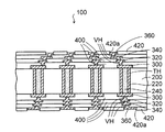
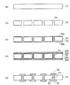
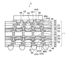
図3〜図6は実施形態の配線基板の製造方法を示す断面図、図7は実施形態の配線基板を示す断面図である。以下、実施形態の配線基板の製造方法を説明しながら配線基板の構造について説明する。
Claims (4)
- 厚みが100μm〜200μmのコア基板と、
前記コア基板の上に形成された第1配線層と、
前記コア基板の上に形成され、前記第1配線層を埋め込む繊維補強材含有樹脂フィルムからなる繊維補強材含有樹脂層と、前記繊維補強材含有樹脂層の上に接着されたプライマーフィルムからなるプライマー層とにより形成される層間絶縁層と、
前記層間絶縁層に形成され、前記第1配線層に到達するビアホールと、
前記プライマー層の上に形成され、前記ビアホールを介して前記第1配線層に接続される第2配線層とを有し、
前記プライマー層は上面が粗化面となったエポキシ樹脂から形成され、前記プライマー層の粗化面の表面粗さ(Ra)は100nm〜600nmであり、
前記ビアホールの内壁の前記プライマー層の表面粗さは、前記プライマー層の粗化面の表面粗さの範囲と同じであり、
前記第2配線層は、前記プライマー層の粗化面と、前記ビアホールの内壁の前記プライマー層とに接して形成されることを特徴とする配線基板。 - 前記第1配線層は、前記コア基板の両面側に形成されて、前記コア基板のスルーホールに形成された導体層を介して相互接続されており、
前記コア基板の両面側に、前記層間絶縁層及び前記第2配線層がそれぞれ形成されていることを特徴とする請求項1に記載の配線基板。 - 厚みが100μm〜200μmのコア基板の上に第1配線層を形成する工程と、
繊維補強材含有樹脂フィルムの一方の面にプライマーフィルムが接着された積層フィルムを用意する工程と、
前記コア基板の上に、前記積層フィルムを熱プレスすることにより、前記第1配線層を埋め込む繊維補強材含有樹脂層と、エポキシ樹脂からなるプライマー層とが順に積層された積層体を形成して層間絶縁層を得る工程と、
前記層間絶縁層に、前記第1配線層に到達するビアホールを形成する工程と、
前記ビアホール内をデスミア処理して、前記デスミア処理によって前記プライマー層の表面を、表面粗さ(Ra)が100nm〜600nmの粗化面にする工程と、
前記プライマー層の粗化面の上に、前記ビアホールを介して前記第1配線層に接続される第2配線層を形成する工程とを有し、
前記ビアホールの内壁の前記プライマー層の表面粗さは、前記プライマー層の粗化面の表面粗さの範囲と同じに設定され、
前記第2配線層は、前記プライマー層の粗化面と、前記ビアホールの内壁の前記プライマー層とに接して形成されることを特徴とする配線基板の製造方法。 - 前記第1配線層は前記コア基板の両面側に形成され、前記コア基板のスルーホールに形成された導体層を介して相互接続されており、
前記層間絶縁層を得る工程、前記ビアホールを形成する工程、及び前記第2配線層を形成する工程は、前記コア基板の両面側で行われることを特徴とする請求項3に記載の配線基板の製造方法。
Priority Applications (5)
| Application Number | Priority Date | Filing Date | Title |
|---|---|---|---|
| JP2012135592A JP6208411B2 (ja) | 2012-06-15 | 2012-06-15 | 配線基板及びその製造方法 |
| KR1020130065791A KR102049327B1 (ko) | 2012-06-15 | 2013-06-10 | 배선 기판 및 그 제조 방법 |
| CN201310232621.8A CN103517548B (zh) | 2012-06-15 | 2013-06-13 | 布线基板及其制造方法 |
| TW102121131A TWI587764B (zh) | 2012-06-15 | 2013-06-14 | 佈線基板及其製造方法 |
| US13/917,818 US9252096B2 (en) | 2012-06-15 | 2013-06-14 | Wiring substrate and method of manufacturing the same |
Applications Claiming Priority (1)
| Application Number | Priority Date | Filing Date | Title |
|---|---|---|---|
| JP2012135592A JP6208411B2 (ja) | 2012-06-15 | 2012-06-15 | 配線基板及びその製造方法 |
Publications (3)
| Publication Number | Publication Date |
|---|---|
| JP2014003054A JP2014003054A (ja) | 2014-01-09 |
| JP2014003054A5 JP2014003054A5 (ja) | 2015-07-09 |
| JP6208411B2 true JP6208411B2 (ja) | 2017-10-04 |
Family
ID=49755160
Family Applications (1)
| Application Number | Title | Priority Date | Filing Date |
|---|---|---|---|
| JP2012135592A Active JP6208411B2 (ja) | 2012-06-15 | 2012-06-15 | 配線基板及びその製造方法 |
Country Status (5)
| Country | Link |
|---|---|
| US (1) | US9252096B2 (ja) |
| JP (1) | JP6208411B2 (ja) |
| KR (1) | KR102049327B1 (ja) |
| CN (1) | CN103517548B (ja) |
| TW (1) | TWI587764B (ja) |
Families Citing this family (9)
| Publication number | Priority date | Publication date | Assignee | Title |
|---|---|---|---|---|
| JP2015065322A (ja) * | 2013-09-25 | 2015-04-09 | 日東電工株式会社 | 半導体装置の製造方法 |
| JP6075789B2 (ja) * | 2014-01-31 | 2017-02-08 | 京セラ株式会社 | 配線基板の製造方法 |
| CN105307386B (zh) * | 2015-09-15 | 2018-07-06 | 三星半导体(中国)研究开发有限公司 | 印刷电路板以及包括其的半导体封装件 |
| US10643936B2 (en) * | 2017-05-31 | 2020-05-05 | Dyi-chung Hu | Package substrate and package structure |
| JP7207192B2 (ja) * | 2019-06-19 | 2023-01-18 | Tdk株式会社 | センサー用パッケージ基板及びこれを備えるセンサーモジュール、並びに、センサー用パッケージ基板の製造方法 |
| JP7364383B2 (ja) * | 2019-07-19 | 2023-10-18 | 株式会社 大昌電子 | プリント配線板の製造方法 |
| US11439022B2 (en) | 2019-09-02 | 2022-09-06 | Samsung Electro-Mechanics Co., Ltd. | Printed circuit board |
| CN111366839B (zh) * | 2020-03-28 | 2022-04-12 | 深圳中科系统集成技术有限公司 | 一种晶圆测试用探针转接板及其制作方法 |
| TWI751554B (zh) * | 2020-05-12 | 2022-01-01 | 台灣愛司帝科技股份有限公司 | 影像顯示器及其拼接式電路承載與控制模組 |
Family Cites Families (17)
| Publication number | Priority date | Publication date | Assignee | Title |
|---|---|---|---|---|
| JPH1117345A (ja) * | 1997-06-19 | 1999-01-22 | Ibiden Co Ltd | 多層プリント配線板 |
| JP3373406B2 (ja) * | 1997-10-14 | 2003-02-04 | イビデン株式会社 | プリント配線板およびその製造方法 |
| CN100383278C (zh) * | 2002-02-28 | 2008-04-23 | 日本瑞翁株式会社 | 部分镀敷方法、部分镀敷树脂基材以及多层电路基板的制造方法 |
| JP4488684B2 (ja) * | 2002-08-09 | 2010-06-23 | イビデン株式会社 | 多層プリント配線板 |
| KR101131759B1 (ko) * | 2003-04-07 | 2012-04-06 | 이비덴 가부시키가이샤 | 다층프린트배선판 |
| JP2006086233A (ja) * | 2004-09-14 | 2006-03-30 | Sumitomo Bakelite Co Ltd | 多層配線板およびその製造方法 |
| JP2007150221A (ja) * | 2005-10-27 | 2007-06-14 | Fujitsu Ltd | 多層回路基板およびその製造方法 |
| JP2008085111A (ja) * | 2006-09-28 | 2008-04-10 | Matsushita Electric Ind Co Ltd | 配線基板とその製造方法 |
| JP5042762B2 (ja) * | 2007-09-27 | 2012-10-03 | 株式会社テラミクロス | 半導体装置 |
| JP5094323B2 (ja) * | 2007-10-15 | 2012-12-12 | 新光電気工業株式会社 | 配線基板の製造方法 |
| JP2010010329A (ja) | 2008-06-26 | 2010-01-14 | Kyocer Slc Technologies Corp | 配線基板およびその製造方法 |
| JP4844904B2 (ja) | 2009-03-27 | 2011-12-28 | Tdk株式会社 | 多層配線板及びその製造方法 |
| US8161637B2 (en) * | 2009-07-24 | 2012-04-24 | Ibiden Co., Ltd. | Manufacturing method for printed wiring board |
| TWI471073B (zh) * | 2009-12-31 | 2015-01-21 | Unimicron Technology Corp | 線路基板及其製作方法 |
| JP5341796B2 (ja) | 2010-02-26 | 2013-11-13 | 京セラSlcテクノロジー株式会社 | 配線基板の製造方法 |
| WO2011138865A1 (ja) | 2010-05-07 | 2011-11-10 | 住友ベークライト株式会社 | 回路基板用エポキシ樹脂組成物、プリプレグ、積層板、樹脂シート、プリント配線板用積層基材、プリント配線板、及び半導体装置 |
| JP2012069926A (ja) * | 2010-08-21 | 2012-04-05 | Ibiden Co Ltd | プリント配線板及びプリント配線板の製造方法 |
-
2012
- 2012-06-15 JP JP2012135592A patent/JP6208411B2/ja active Active
-
2013
- 2013-06-10 KR KR1020130065791A patent/KR102049327B1/ko active IP Right Grant
- 2013-06-13 CN CN201310232621.8A patent/CN103517548B/zh active Active
- 2013-06-14 US US13/917,818 patent/US9252096B2/en active Active
- 2013-06-14 TW TW102121131A patent/TWI587764B/zh active
Also Published As
| Publication number | Publication date |
|---|---|
| CN103517548A (zh) | 2014-01-15 |
| US20130334703A1 (en) | 2013-12-19 |
| KR102049327B1 (ko) | 2019-11-28 |
| US9252096B2 (en) | 2016-02-02 |
| TW201406240A (zh) | 2014-02-01 |
| JP2014003054A (ja) | 2014-01-09 |
| CN103517548B (zh) | 2018-03-06 |
| TWI587764B (zh) | 2017-06-11 |
| KR20130141372A (ko) | 2013-12-26 |
Similar Documents
| Publication | Publication Date | Title |
|---|---|---|
| JP6208411B2 (ja) | 配線基板及びその製造方法 | |
| JP6200178B2 (ja) | 電子部品内蔵基板及びその製造方法 | |
| JP5410660B2 (ja) | 配線基板及びその製造方法と電子部品装置及びその製造方法 | |
| US10745819B2 (en) | Printed wiring board, semiconductor package and method for manufacturing printed wiring board | |
| JP5662551B1 (ja) | 配線基板、半導体装置及び配線基板の製造方法 | |
| KR101906883B1 (ko) | 배선 기판 및 그 제조 방법 | |
| JP6009228B2 (ja) | 電子部品内蔵基板の製造方法 | |
| JP6358431B2 (ja) | 電子部品装置及びその製造方法 | |
| US10098243B2 (en) | Printed wiring board and semiconductor package | |
| WO2010074121A1 (ja) | プリント配線板の製造方法 | |
| JP6158601B2 (ja) | 配線基板及び配線基板の製造方法 | |
| US9392684B2 (en) | Wiring substrate and method for manufacturing wiring substrate | |
| US9137896B2 (en) | Wiring substrate | |
| JP6092555B2 (ja) | 配線基板の製造方法 | |
| JP2010034197A (ja) | ビルドアップ基板 | |
| JP5432354B2 (ja) | 配線基板製造用の仮基板及びその製造方法 | |
| JP2014090079A (ja) | プリント配線板 | |
| JP4892924B2 (ja) | 多層プリント配線基板及びその製造方法 | |
| JP5565953B2 (ja) | 配線基板およびその製造方法 | |
| KR101108816B1 (ko) | 다층 인쇄회로기판 및 이의 제조방법 | |
| JP6343058B2 (ja) | 配線基板及び配線基板の製造方法 | |
| JP6367902B2 (ja) | 配線基板 | |
| JP6075789B2 (ja) | 配線基板の製造方法 | |
| JP2014045018A (ja) | プリント配線板 |
Legal Events
| Date | Code | Title | Description |
|---|---|---|---|
| A521 | Written amendment |
Free format text: JAPANESE INTERMEDIATE CODE: A523 Effective date: 20150526 |
|
| A621 | Written request for application examination |
Free format text: JAPANESE INTERMEDIATE CODE: A621 Effective date: 20150526 |
|
| A977 | Report on retrieval |
Free format text: JAPANESE INTERMEDIATE CODE: A971007 Effective date: 20160219 |
|
| A131 | Notification of reasons for refusal |
Free format text: JAPANESE INTERMEDIATE CODE: A131 Effective date: 20160301 |
|
| A521 | Written amendment |
Free format text: JAPANESE INTERMEDIATE CODE: A523 Effective date: 20160421 |
|
| A02 | Decision of refusal |
Free format text: JAPANESE INTERMEDIATE CODE: A02 Effective date: 20160524 |
|
| A521 | Written amendment |
Free format text: JAPANESE INTERMEDIATE CODE: A523 Effective date: 20160810 |
|
| A911 | Transfer to examiner for re-examination before appeal (zenchi) |
Free format text: JAPANESE INTERMEDIATE CODE: A911 Effective date: 20160819 |
|
| A912 | Re-examination (zenchi) completed and case transferred to appeal board |
Free format text: JAPANESE INTERMEDIATE CODE: A912 Effective date: 20161021 |
|
| A521 | Written amendment |
Free format text: JAPANESE INTERMEDIATE CODE: A523 Effective date: 20170515 |
|
| A61 | First payment of annual fees (during grant procedure) |
Free format text: JAPANESE INTERMEDIATE CODE: A61 Effective date: 20170907 |
|
| R150 | Certificate of patent or registration of utility model |
Ref document number: 6208411 Country of ref document: JP Free format text: JAPANESE INTERMEDIATE CODE: R150 |