JP6110593B2 - 半導体装置 - Google Patents
半導体装置 Download PDFInfo
- Publication number
- JP6110593B2 JP6110593B2 JP2012013833A JP2012013833A JP6110593B2 JP 6110593 B2 JP6110593 B2 JP 6110593B2 JP 2012013833 A JP2012013833 A JP 2012013833A JP 2012013833 A JP2012013833 A JP 2012013833A JP 6110593 B2 JP6110593 B2 JP 6110593B2
- Authority
- JP
- Japan
- Prior art keywords
- oxide semiconductor
- film
- transistor
- insulating film
- semiconductor film
- Prior art date
- Legal status (The legal status is an assumption and is not a legal conclusion. Google has not performed a legal analysis and makes no representation as to the accuracy of the status listed.)
- Expired - Fee Related
Links
Images


Classifications
-
- H—ELECTRICITY
- H10—SEMICONDUCTOR DEVICES; ELECTRIC SOLID-STATE DEVICES NOT OTHERWISE PROVIDED FOR
- H10D—INORGANIC ELECTRIC SEMICONDUCTOR DEVICES
- H10D30/00—Field-effect transistors [FET]
- H10D30/60—Insulated-gate field-effect transistors [IGFET]
- H10D30/67—Thin-film transistors [TFT]
- H10D30/6757—Thin-film transistors [TFT] characterised by the structure of the channel, e.g. transverse or longitudinal shape or doping profile
-
- H—ELECTRICITY
- H10—SEMICONDUCTOR DEVICES; ELECTRIC SOLID-STATE DEVICES NOT OTHERWISE PROVIDED FOR
- H10D—INORGANIC ELECTRIC SEMICONDUCTOR DEVICES
- H10D30/00—Field-effect transistors [FET]
- H10D30/60—Insulated-gate field-effect transistors [IGFET]
- H10D30/67—Thin-film transistors [TFT]
- H10D30/674—Thin-film transistors [TFT] characterised by the active materials
- H10D30/6755—Oxide semiconductors, e.g. zinc oxide, copper aluminium oxide or cadmium stannate
-
- H—ELECTRICITY
- H10—SEMICONDUCTOR DEVICES; ELECTRIC SOLID-STATE DEVICES NOT OTHERWISE PROVIDED FOR
- H10B—ELECTRONIC MEMORY DEVICES
- H10B12/00—Dynamic random access memory [DRAM] devices
-
- H—ELECTRICITY
- H10—SEMICONDUCTOR DEVICES; ELECTRIC SOLID-STATE DEVICES NOT OTHERWISE PROVIDED FOR
- H10D—INORGANIC ELECTRIC SEMICONDUCTOR DEVICES
- H10D30/00—Field-effect transistors [FET]
- H10D30/60—Insulated-gate field-effect transistors [IGFET]
- H10D30/67—Thin-film transistors [TFT]
- H10D30/674—Thin-film transistors [TFT] characterised by the active materials
- H10D30/6755—Oxide semiconductors, e.g. zinc oxide, copper aluminium oxide or cadmium stannate
- H10D30/6756—Amorphous oxide semiconductors
-
- H—ELECTRICITY
- H10—SEMICONDUCTOR DEVICES; ELECTRIC SOLID-STATE DEVICES NOT OTHERWISE PROVIDED FOR
- H10D—INORGANIC ELECTRIC SEMICONDUCTOR DEVICES
- H10D62/00—Semiconductor bodies, or regions thereof, of devices having potential barriers
- H10D62/40—Crystalline structures
- H10D62/402—Amorphous materials
-
- H—ELECTRICITY
- H10—SEMICONDUCTOR DEVICES; ELECTRIC SOLID-STATE DEVICES NOT OTHERWISE PROVIDED FOR
- H10D—INORGANIC ELECTRIC SEMICONDUCTOR DEVICES
- H10D62/00—Semiconductor bodies, or regions thereof, of devices having potential barriers
- H10D62/40—Crystalline structures
- H10D62/405—Orientations of crystalline planes
-
- H—ELECTRICITY
- H10—SEMICONDUCTOR DEVICES; ELECTRIC SOLID-STATE DEVICES NOT OTHERWISE PROVIDED FOR
- H10D—INORGANIC ELECTRIC SEMICONDUCTOR DEVICES
- H10D62/00—Semiconductor bodies, or regions thereof, of devices having potential barriers
- H10D62/80—Semiconductor bodies, or regions thereof, of devices having potential barriers characterised by the materials
-
- H—ELECTRICITY
- H10—SEMICONDUCTOR DEVICES; ELECTRIC SOLID-STATE DEVICES NOT OTHERWISE PROVIDED FOR
- H10D—INORGANIC ELECTRIC SEMICONDUCTOR DEVICES
- H10D86/00—Integrated devices formed in or on insulating or conducting substrates, e.g. formed in silicon-on-insulator [SOI] substrates or on stainless steel or glass substrates
- H10D86/40—Integrated devices formed in or on insulating or conducting substrates, e.g. formed in silicon-on-insulator [SOI] substrates or on stainless steel or glass substrates characterised by multiple TFTs
- H10D86/60—Integrated devices formed in or on insulating or conducting substrates, e.g. formed in silicon-on-insulator [SOI] substrates or on stainless steel or glass substrates characterised by multiple TFTs wherein the TFTs are in active matrices
-
- H—ELECTRICITY
- H10—SEMICONDUCTOR DEVICES; ELECTRIC SOLID-STATE DEVICES NOT OTHERWISE PROVIDED FOR
- H10P—GENERIC PROCESSES OR APPARATUS FOR THE MANUFACTURE OR TREATMENT OF DEVICES COVERED BY CLASS H10
- H10P14/00—Formation of materials, e.g. in the shape of layers or pillars
- H10P14/20—Formation of materials, e.g. in the shape of layers or pillars of semiconductor materials
- H10P14/34—Deposited materials, e.g. layers
- H10P14/3402—Deposited materials, e.g. layers characterised by the chemical composition
- H10P14/3424—Deposited materials, e.g. layers characterised by the chemical composition being Group IIB-VIA materials
- H10P14/3426—Oxides
-
- H—ELECTRICITY
- H10—SEMICONDUCTOR DEVICES; ELECTRIC SOLID-STATE DEVICES NOT OTHERWISE PROVIDED FOR
- H10P—GENERIC PROCESSES OR APPARATUS FOR THE MANUFACTURE OR TREATMENT OF DEVICES COVERED BY CLASS H10
- H10P14/00—Formation of materials, e.g. in the shape of layers or pillars
- H10P14/20—Formation of materials, e.g. in the shape of layers or pillars of semiconductor materials
- H10P14/34—Deposited materials, e.g. layers
- H10P14/3402—Deposited materials, e.g. layers characterised by the chemical composition
- H10P14/3434—Deposited materials, e.g. layers characterised by the chemical composition being oxide semiconductor materials
Landscapes
- Thin Film Transistor (AREA)
- Physical Vapour Deposition (AREA)
Description
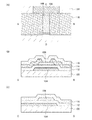
本実施の形態では、本発明の一態様に係るトランジスタの一例について図1を用いて説明する。
本実施の形態では、実施の形態1に示したトランジスタとは異なる構造のトランジスタについて説明する。
本実施の形態では、実施の形態1または実施の形態2に示したトランジスタを用いて作製した液晶表示装置について説明する。なお、本実施の形態では液晶表示装置に本発明の一形態を適用した例について説明するが、これに限定されるものではない。例えば、EL(Electro Luminescence)表示装置に本発明の一形態を適用することも、当業者であれば容易に想到しうるものである。
本実施の形態では、実施の形態1または実施の形態2に示したトランジスタを用いて、半導体記憶装置を作製する例について説明する。
実施の形態1または実施の形態2に示したトランジスタを少なくとも一部に用いてCPU(Central Processing Unit)を構成することができる。
本実施の形態では、実施の形態1乃至実施の形態5の少なくともいずれかを適用した電子機器の例について説明する。

104 ゲート電極
106 酸化物半導体膜
112 ゲート絶縁膜
116 一対の電極
118 層間絶縁膜
200 画素
206 酸化物半導体膜
210 液晶素子
216 一対の電極
218 層間絶縁膜
220 キャパシタ
230 トランジスタ
302 下地絶縁膜
304 ゲート電極
306 酸化物半導体膜
312 ゲート絶縁膜
316 一対の電極
404 ゲート電極
406 酸化物半導体膜
412 ゲート絶縁膜
416 一対の電極
504 ゲート電極
506 酸化物半導体膜
512 ゲート絶縁膜
516 一対の電極
518 層間絶縁膜
521 領域
526 領域
604 ゲート電極
606 酸化物半導体膜
612 ゲート絶縁膜
616 一対の電極
618 層間絶縁膜
621 領域
626 領域
1141 スイッチング素子
1142 記憶素子
1143 記憶素子群
1189 ROMインターフェース
1190 基板
1191 ALU
1192 ALUコントローラ
1193 インストラクションデコーダ
1194 インタラプトコントローラ
1195 タイミングコントローラ
1196 レジスタ
1197 レジスタコントローラ
1198 バスインターフェース
1199 ROM
3001 実線
3002 実線
3003 実線
3004 実線
9300 筐体
9301 ボタン
9302 マイクロフォン
9303 表示部
9304 スピーカ
9305 カメラ
9310 筐体
9311 表示部
9320 筐体
9321 ボタン
9322 マイクロフォン
9323 表示部
Claims (6)
- ゲート電極と、
ゲート絶縁膜と、
一対の電極と、
前記ゲート絶縁膜を介して、前記ゲート電極と少なくとも一部が重畳し、かつ前記一対の電極と少なくとも一部が接するp型酸化物半導体材料を含むn型酸化物半導体膜と、を有し、
前記p型酸化物半導体材料は、Ni、La、Sr、NdまたはNaの少なくともいずれかを含み、
前記ゲート電極は、第1の膜と第2の膜とを有し、
前記第1の膜は、前記ゲート絶縁膜と前記第2の膜との間に設けられ、
前記第1の膜は、1×10 20 cm −3 以上7原子%以下の窒素を含み、且つIn、GaおよびZnを含む酸化物膜であり、
前記第2の膜は、シート抵抗が10Ω/sq以下の膜であることを特徴とする半導体装置。 - ゲート電極と、
ゲート絶縁膜と、
一対の電極と、
前記ゲート絶縁膜を介して、前記ゲート電極と少なくとも一部が重畳し、かつ前記一対の電極と少なくとも一部が接するp型酸化物半導体材料を含むn型酸化物半導体膜と、を有し、
前記p型酸化物半導体材料は、Ni−O系材料、La−Ni−O系材料、Nd−Ni−O系材料、Sr−Cu−O系材料またはLa−Cu−O系材料の少なくともいずれかを含み、
前記ゲート電極は、第1の膜と第2の膜とを有し、
前記第1の膜は、前記ゲート絶縁膜と前記第2の膜との間に設けられ、
前記第1の膜は、1×10 20 cm −3 以上7原子%以下の窒素を含み、且つIn、GaおよびZnを含む酸化物膜であり、
前記第2の膜は、シート抵抗が10Ω/sq以下の膜であることを特徴とする半導体装置。 - 請求項1または請求項2において、
前記n型酸化物半導体膜に対し、前記p型酸化物半導体材料が0.001以上0.15以下の原子数比で含まれることを特徴とする半導体装置。 - 請求項1乃至請求項3のいずれか一において、
前記n型酸化物半導体膜に対し、酸化シリコンおよび酸化ゲルマニウムの少なくともいずれかが0.01以上0.2以下の原子数比で含まれることを特徴とする半導体装置。 - 請求項1乃至請求項4のいずれか一において、
前記n型酸化物半導体膜は、In、Ga、ZnおよびSnから選ばれた二種以上を含むことを特徴とする半導体装置。 - 請求項1乃至請求項5のいずれか一において、
前記n型酸化物半導体膜が非晶質であることを特徴とする半導体装置。
Priority Applications (1)
| Application Number | Priority Date | Filing Date | Title |
|---|---|---|---|
| JP2012013833A JP6110593B2 (ja) | 2011-01-27 | 2012-01-26 | 半導体装置 |
Applications Claiming Priority (3)
| Application Number | Priority Date | Filing Date | Title |
|---|---|---|---|
| JP2011014652 | 2011-01-27 | ||
| JP2011014652 | 2011-01-27 | ||
| JP2012013833A JP6110593B2 (ja) | 2011-01-27 | 2012-01-26 | 半導体装置 |
Publications (2)
| Publication Number | Publication Date |
|---|---|
| JP2012169612A JP2012169612A (ja) | 2012-09-06 |
| JP6110593B2 true JP6110593B2 (ja) | 2017-04-05 |
Family
ID=46576601
Family Applications (1)
| Application Number | Title | Priority Date | Filing Date |
|---|---|---|---|
| JP2012013833A Expired - Fee Related JP6110593B2 (ja) | 2011-01-27 | 2012-01-26 | 半導体装置 |
Country Status (5)
| Country | Link |
|---|---|
| US (2) | US8890150B2 (ja) |
| JP (1) | JP6110593B2 (ja) |
| KR (2) | KR20190007525A (ja) |
| TW (1) | TWI553860B (ja) |
| WO (1) | WO2012102181A1 (ja) |
Families Citing this family (14)
| Publication number | Priority date | Publication date | Assignee | Title |
|---|---|---|---|---|
| US9786793B2 (en) * | 2012-03-29 | 2017-10-10 | Semiconductor Energy Laboratory Co., Ltd. | Semiconductor device comprising oxide semiconductor layer including regions with different concentrations of resistance-reducing elements |
| KR102495290B1 (ko) * | 2012-12-28 | 2023-02-06 | 가부시키가이샤 한도오따이 에네루기 켄큐쇼 | 반도체 장치 |
| US9443876B2 (en) * | 2014-02-05 | 2016-09-13 | Semiconductor Energy Laboratory Co., Ltd. | Semiconductor device, display device including the semiconductor device, display module including the display device, and electronic device including the semiconductor device, the display device, and the display module |
| WO2015142038A1 (ko) | 2014-03-17 | 2015-09-24 | 경희대학교 산학협력단 | 갈륨을 포함하는 p형 비정질 산화물 반도체, 이의 제조방법, 이를 포함하는 태양전지 및 이의 제조 방법 |
| KR101596569B1 (ko) * | 2014-03-17 | 2016-02-23 | 경희대학교 산학협력단 | 갈륨을 포함하는 p형 비정질 산화물 반도체, 및 이의 제조방법 |
| US9985139B2 (en) | 2014-11-12 | 2018-05-29 | Qualcomm Incorporated | Hydrogenated p-channel metal oxide semiconductor thin film transistors |
| US9685542B2 (en) | 2014-12-30 | 2017-06-20 | Qualcomm Incorporated | Atomic layer deposition of P-type oxide semiconductor thin films |
| US9647135B2 (en) * | 2015-01-22 | 2017-05-09 | Snaptrack, Inc. | Tin based p-type oxide semiconductor and thin film transistor applications |
| JP2016219483A (ja) * | 2015-05-15 | 2016-12-22 | 株式会社半導体エネルギー研究所 | 半導体装置 |
| JP7037145B2 (ja) * | 2017-03-02 | 2022-03-16 | 大阪ガスケミカル株式会社 | フルオレン化合物を含有する発光体 |
| CN107919400B (zh) * | 2017-10-09 | 2020-10-02 | 上海集成电路研发中心有限公司 | 一种InSe晶体管及其制备方法 |
| US10756116B2 (en) | 2018-03-20 | 2020-08-25 | Sharp Kabushiki Kaisha | Active matrix substrate having thin film transistors that each include copper gate electrode and oxide semiconductor layer |
| JP6706653B2 (ja) * | 2018-03-20 | 2020-06-10 | シャープ株式会社 | アクティブマトリクス基板 |
| EP4270478A4 (en) * | 2022-03-15 | 2023-11-22 | Changxin Memory Technologies, Inc. | MEMORY AND ASSOCIATED PREPARATION METHOD |
Family Cites Families (120)
| Publication number | Priority date | Publication date | Assignee | Title |
|---|---|---|---|---|
| JPS60198861A (ja) | 1984-03-23 | 1985-10-08 | Fujitsu Ltd | 薄膜トランジスタ |
| JPH0244256B2 (ja) | 1987-01-28 | 1990-10-03 | Kagaku Gijutsucho Mukizaishitsu Kenkyushocho | Ingazn2o5deshimesarerurotsuhoshokeinosojokozoojusurukagobutsuoyobisonoseizoho |
| JPH0244260B2 (ja) | 1987-02-24 | 1990-10-03 | Kagaku Gijutsucho Mukizaishitsu Kenkyushocho | Ingazn5o8deshimesarerurotsuhoshokeinosojokozoojusurukagobutsuoyobisonoseizoho |
| JPH0244258B2 (ja) | 1987-02-24 | 1990-10-03 | Kagaku Gijutsucho Mukizaishitsu Kenkyushocho | Ingazn3o6deshimesarerurotsuhoshokeinosojokozoojusurukagobutsuoyobisonoseizoho |
| JPS63210023A (ja) | 1987-02-24 | 1988-08-31 | Natl Inst For Res In Inorg Mater | InGaZn↓4O↓7で示される六方晶系の層状構造を有する化合物およびその製造法 |
| JPH0244262B2 (ja) | 1987-02-27 | 1990-10-03 | Kagaku Gijutsucho Mukizaishitsu Kenkyushocho | Ingazn6o9deshimesarerurotsuhoshokeinosojokozoojusurukagobutsuoyobisonoseizoho |
| JPH0244263B2 (ja) | 1987-04-22 | 1990-10-03 | Kagaku Gijutsucho Mukizaishitsu Kenkyushocho | Ingazn7o10deshimesarerurotsuhoshokeinosojokozoojusurukagobutsuoyobisonoseizoho |
| JPH05251705A (ja) | 1992-03-04 | 1993-09-28 | Fuji Xerox Co Ltd | 薄膜トランジスタ |
| JP3298974B2 (ja) | 1993-03-23 | 2002-07-08 | 電子科学株式会社 | 昇温脱離ガス分析装置 |
| JP3479375B2 (ja) | 1995-03-27 | 2003-12-15 | 科学技術振興事業団 | 亜酸化銅等の金属酸化物半導体による薄膜トランジスタとpn接合を形成した金属酸化物半導体装置およびそれらの製造方法 |
| US5614727A (en) | 1995-06-06 | 1997-03-25 | International Business Machines Corporation | Thin film diode having large current capability with low turn-on voltages for integrated devices |
| JPH11505377A (ja) | 1995-08-03 | 1999-05-18 | フィリップス エレクトロニクス ネムローゼ フェンノートシャップ | 半導体装置 |
| JP3625598B2 (ja) | 1995-12-30 | 2005-03-02 | 三星電子株式会社 | 液晶表示装置の製造方法 |
| JP4170454B2 (ja) | 1998-07-24 | 2008-10-22 | Hoya株式会社 | 透明導電性酸化物薄膜を有する物品及びその製造方法 |
| JP2000150861A (ja) | 1998-11-16 | 2000-05-30 | Tdk Corp | 酸化物薄膜 |
| JP3276930B2 (ja) | 1998-11-17 | 2002-04-22 | 科学技術振興事業団 | トランジスタ及び半導体装置 |
| TW460731B (en) | 1999-09-03 | 2001-10-21 | Ind Tech Res Inst | Electrode structure and production method of wide viewing angle LCD |
| JP4089858B2 (ja) | 2000-09-01 | 2008-05-28 | 国立大学法人東北大学 | 半導体デバイス |
| KR20020038482A (ko) | 2000-11-15 | 2002-05-23 | 모리시타 요이찌 | 박막 트랜지스터 어레이, 그 제조방법 및 그것을 이용한표시패널 |
| JP3997731B2 (ja) | 2001-03-19 | 2007-10-24 | 富士ゼロックス株式会社 | 基材上に結晶性半導体薄膜を形成する方法 |
| JP2002289859A (ja) | 2001-03-23 | 2002-10-04 | Minolta Co Ltd | 薄膜トランジスタ |
| JP3925839B2 (ja) | 2001-09-10 | 2007-06-06 | シャープ株式会社 | 半導体記憶装置およびその試験方法 |
| JP4090716B2 (ja) | 2001-09-10 | 2008-05-28 | 雅司 川崎 | 薄膜トランジスタおよびマトリクス表示装置 |
| EP1443130B1 (en) | 2001-11-05 | 2011-09-28 | Japan Science and Technology Agency | Natural superlattice homologous single crystal thin film, method for preparation thereof, and device using said single crystal thin film |
| JP4164562B2 (ja) | 2002-09-11 | 2008-10-15 | 独立行政法人科学技術振興機構 | ホモロガス薄膜を活性層として用いる透明薄膜電界効果型トランジスタ |
| JP4083486B2 (ja) | 2002-02-21 | 2008-04-30 | 独立行政法人科学技術振興機構 | LnCuO(S,Se,Te)単結晶薄膜の製造方法 |
| US7049190B2 (en) | 2002-03-15 | 2006-05-23 | Sanyo Electric Co., Ltd. | Method for forming ZnO film, method for forming ZnO semiconductor layer, method for fabricating semiconductor device, and semiconductor device |
| JP3933591B2 (ja) | 2002-03-26 | 2007-06-20 | 淳二 城戸 | 有機エレクトロルミネッセント素子 |
| US7339187B2 (en) | 2002-05-21 | 2008-03-04 | State Of Oregon Acting By And Through The Oregon State Board Of Higher Education On Behalf Of Oregon State University | Transistor structures |
| JP2004022625A (ja) | 2002-06-13 | 2004-01-22 | Murata Mfg Co Ltd | 半導体デバイス及び該半導体デバイスの製造方法 |
| US7105868B2 (en) | 2002-06-24 | 2006-09-12 | Cermet, Inc. | High-electron mobility transistor with zinc oxide |
| US7067843B2 (en) | 2002-10-11 | 2006-06-27 | E. I. Du Pont De Nemours And Company | Transparent oxide semiconductor thin film transistors |
| JP4166105B2 (ja) | 2003-03-06 | 2008-10-15 | シャープ株式会社 | 半導体装置およびその製造方法 |
| JP2004273732A (ja) | 2003-03-07 | 2004-09-30 | Sharp Corp | アクティブマトリクス基板およびその製造方法 |
| JP4108633B2 (ja) | 2003-06-20 | 2008-06-25 | シャープ株式会社 | 薄膜トランジスタおよびその製造方法ならびに電子デバイス |
| US7262463B2 (en) | 2003-07-25 | 2007-08-28 | Hewlett-Packard Development Company, L.P. | Transistor including a deposited channel region having a doped portion |
| EP1737044B1 (en) | 2004-03-12 | 2014-12-10 | Japan Science and Technology Agency | Amorphous oxide and thin film transistor |
| US7282782B2 (en) | 2004-03-12 | 2007-10-16 | Hewlett-Packard Development Company, L.P. | Combined binary oxide semiconductor device |
| US7297977B2 (en) | 2004-03-12 | 2007-11-20 | Hewlett-Packard Development Company, L.P. | Semiconductor device |
| US7145174B2 (en) | 2004-03-12 | 2006-12-05 | Hewlett-Packard Development Company, Lp. | Semiconductor device |
| US7211825B2 (en) | 2004-06-14 | 2007-05-01 | Yi-Chi Shih | Indium oxide-based thin film transistors and circuits |
| WO2006009413A1 (en) * | 2004-07-23 | 2006-01-26 | Gwangju Institute Of Science And Technology | Top-emitting light emitting diodes and method of manufacturing thereof |
| JP2006100760A (ja) | 2004-09-02 | 2006-04-13 | Casio Comput Co Ltd | 薄膜トランジスタおよびその製造方法 |
| US7285501B2 (en) | 2004-09-17 | 2007-10-23 | Hewlett-Packard Development Company, L.P. | Method of forming a solution processed device |
| US7298084B2 (en) | 2004-11-02 | 2007-11-20 | 3M Innovative Properties Company | Methods and displays utilizing integrated zinc oxide row and column drivers in conjunction with organic light emitting diodes |
| RU2358354C2 (ru) | 2004-11-10 | 2009-06-10 | Кэнон Кабусики Кайся | Светоизлучающее устройство |
| JP5138163B2 (ja) * | 2004-11-10 | 2013-02-06 | キヤノン株式会社 | 電界効果型トランジスタ |
| US7791072B2 (en) | 2004-11-10 | 2010-09-07 | Canon Kabushiki Kaisha | Display |
| KR100998527B1 (ko) | 2004-11-10 | 2010-12-07 | 고쿠리츠다이가쿠호진 토쿄고교 다이가꾸 | 비정질 산화물 및 전계 효과 트랜지스터 |
| US7829444B2 (en) | 2004-11-10 | 2010-11-09 | Canon Kabushiki Kaisha | Field effect transistor manufacturing method |
| US7863611B2 (en) | 2004-11-10 | 2011-01-04 | Canon Kabushiki Kaisha | Integrated circuits utilizing amorphous oxides |
| US7453065B2 (en) | 2004-11-10 | 2008-11-18 | Canon Kabushiki Kaisha | Sensor and image pickup device |
| EP1815530B1 (en) | 2004-11-10 | 2021-02-17 | Canon Kabushiki Kaisha | Field effect transistor employing an amorphous oxide |
| US7579224B2 (en) | 2005-01-21 | 2009-08-25 | Semiconductor Energy Laboratory Co., Ltd. | Method for manufacturing a thin film semiconductor device |
| TWI505473B (zh) | 2005-01-28 | 2015-10-21 | 半導體能源研究所股份有限公司 | 半導體裝置,電子裝置,和半導體裝置的製造方法 |
| TWI481024B (zh) | 2005-01-28 | 2015-04-11 | 半導體能源研究所股份有限公司 | 半導體裝置,電子裝置,和半導體裝置的製造方法 |
| US7858451B2 (en) | 2005-02-03 | 2010-12-28 | Semiconductor Energy Laboratory Co., Ltd. | Electronic device, semiconductor device and manufacturing method thereof |
| US7948171B2 (en) | 2005-02-18 | 2011-05-24 | Semiconductor Energy Laboratory Co., Ltd. | Light emitting device |
| US20060197092A1 (en) | 2005-03-03 | 2006-09-07 | Randy Hoffman | System and method for forming conductive material on a substrate |
| US8681077B2 (en) | 2005-03-18 | 2014-03-25 | Semiconductor Energy Laboratory Co., Ltd. | Semiconductor device, and display device, driving method and electronic apparatus thereof |
| US7544967B2 (en) | 2005-03-28 | 2009-06-09 | Massachusetts Institute Of Technology | Low voltage flexible organic/transparent transistor for selective gas sensing, photodetecting and CMOS device applications |
| US7645478B2 (en) | 2005-03-31 | 2010-01-12 | 3M Innovative Properties Company | Methods of making displays |
| US8300031B2 (en) | 2005-04-20 | 2012-10-30 | Semiconductor Energy Laboratory Co., Ltd. | Semiconductor device comprising transistor having gate and drain connected through a current-voltage conversion element |
| JP2006344849A (ja) | 2005-06-10 | 2006-12-21 | Casio Comput Co Ltd | 薄膜トランジスタ |
| US7402506B2 (en) | 2005-06-16 | 2008-07-22 | Eastman Kodak Company | Methods of making thin film transistors comprising zinc-oxide-based semiconductor materials and transistors made thereby |
| US7691666B2 (en) | 2005-06-16 | 2010-04-06 | Eastman Kodak Company | Methods of making thin film transistors comprising zinc-oxide-based semiconductor materials and transistors made thereby |
| US7507618B2 (en) | 2005-06-27 | 2009-03-24 | 3M Innovative Properties Company | Method for making electronic devices using metal oxide nanoparticles |
| KR100711890B1 (ko) | 2005-07-28 | 2007-04-25 | 삼성에스디아이 주식회사 | 유기 발광표시장치 및 그의 제조방법 |
| JP2007059128A (ja) | 2005-08-23 | 2007-03-08 | Canon Inc | 有機el表示装置およびその製造方法 |
| JP4280736B2 (ja) | 2005-09-06 | 2009-06-17 | キヤノン株式会社 | 半導体素子 |
| JP4850457B2 (ja) | 2005-09-06 | 2012-01-11 | キヤノン株式会社 | 薄膜トランジスタ及び薄膜ダイオード |
| JP5116225B2 (ja) | 2005-09-06 | 2013-01-09 | キヤノン株式会社 | 酸化物半導体デバイスの製造方法 |
| JP2007073705A (ja) | 2005-09-06 | 2007-03-22 | Canon Inc | 酸化物半導体チャネル薄膜トランジスタおよびその製造方法 |
| JP5064747B2 (ja) | 2005-09-29 | 2012-10-31 | 株式会社半導体エネルギー研究所 | 半導体装置、電気泳動表示装置、表示モジュール、電子機器、及び半導体装置の作製方法 |
| EP1998373A3 (en) | 2005-09-29 | 2012-10-31 | Semiconductor Energy Laboratory Co, Ltd. | Semiconductor device having oxide semiconductor layer and manufacturing method thereof |
| JP5078246B2 (ja) | 2005-09-29 | 2012-11-21 | 株式会社半導体エネルギー研究所 | 半導体装置、及び半導体装置の作製方法 |
| JP5037808B2 (ja) | 2005-10-20 | 2012-10-03 | キヤノン株式会社 | アモルファス酸化物を用いた電界効果型トランジスタ、及び該トランジスタを用いた表示装置 |
| CN101577231B (zh) | 2005-11-15 | 2013-01-02 | 株式会社半导体能源研究所 | 半导体器件及其制造方法 |
| TWI292281B (en) | 2005-12-29 | 2008-01-01 | Ind Tech Res Inst | Pixel structure of active organic light emitting diode and method of fabricating the same |
| US7867636B2 (en) | 2006-01-11 | 2011-01-11 | Murata Manufacturing Co., Ltd. | Transparent conductive film and method for manufacturing the same |
| JP4977478B2 (ja) | 2006-01-21 | 2012-07-18 | 三星電子株式会社 | ZnOフィルム及びこれを用いたTFTの製造方法 |
| US7576394B2 (en) | 2006-02-02 | 2009-08-18 | Kochi Industrial Promotion Center | Thin film transistor including low resistance conductive thin films and manufacturing method thereof |
| US7977169B2 (en) | 2006-02-15 | 2011-07-12 | Kochi Industrial Promotion Center | Semiconductor device including active layer made of zinc oxide with controlled orientations and manufacturing method thereof |
| KR20070101595A (ko) | 2006-04-11 | 2007-10-17 | 삼성전자주식회사 | ZnO TFT |
| US20070252928A1 (en) | 2006-04-28 | 2007-11-01 | Toppan Printing Co., Ltd. | Structure, transmission type liquid crystal display, reflection type display and manufacturing method thereof |
| JP5105044B2 (ja) * | 2006-05-09 | 2012-12-19 | 株式会社ブリヂストン | 酸化物トランジスタ及びその製造方法 |
| JP5028033B2 (ja) | 2006-06-13 | 2012-09-19 | キヤノン株式会社 | 酸化物半導体膜のドライエッチング方法 |
| JP4999400B2 (ja) | 2006-08-09 | 2012-08-15 | キヤノン株式会社 | 酸化物半導体膜のドライエッチング方法 |
| JP4609797B2 (ja) | 2006-08-09 | 2011-01-12 | Nec液晶テクノロジー株式会社 | 薄膜デバイス及びその製造方法 |
| JP4332545B2 (ja) | 2006-09-15 | 2009-09-16 | キヤノン株式会社 | 電界効果型トランジスタ及びその製造方法 |
| JP4274219B2 (ja) | 2006-09-27 | 2009-06-03 | セイコーエプソン株式会社 | 電子デバイス、有機エレクトロルミネッセンス装置、有機薄膜半導体装置 |
| JP5164357B2 (ja) | 2006-09-27 | 2013-03-21 | キヤノン株式会社 | 半導体装置及び半導体装置の製造方法 |
| US7622371B2 (en) | 2006-10-10 | 2009-11-24 | Hewlett-Packard Development Company, L.P. | Fused nanocrystal thin film semiconductor and method |
| US7772021B2 (en) | 2006-11-29 | 2010-08-10 | Samsung Electronics Co., Ltd. | Flat panel displays comprising a thin-film transistor having a semiconductive oxide in its channel and methods of fabricating the same for use in flat panel displays |
| JP2008140684A (ja) | 2006-12-04 | 2008-06-19 | Toppan Printing Co Ltd | カラーelディスプレイおよびその製造方法 |
| KR101303578B1 (ko) | 2007-01-05 | 2013-09-09 | 삼성전자주식회사 | 박막 식각 방법 |
| US8207063B2 (en) | 2007-01-26 | 2012-06-26 | Eastman Kodak Company | Process for atomic layer deposition |
| KR101312259B1 (ko) * | 2007-02-09 | 2013-09-25 | 삼성전자주식회사 | 박막 트랜지스터 및 그 제조방법 |
| KR100851215B1 (ko) | 2007-03-14 | 2008-08-07 | 삼성에스디아이 주식회사 | 박막 트랜지스터 및 이를 이용한 유기 전계 발광표시장치 |
| WO2008117739A1 (ja) | 2007-03-23 | 2008-10-02 | Idemitsu Kosan Co., Ltd. | 半導体デバイス、多結晶半導体薄膜、多結晶半導体薄膜の製造方法、電界効果型トランジスタ、及び、電界効果型トランジスタの製造方法 |
| US7795613B2 (en) | 2007-04-17 | 2010-09-14 | Toppan Printing Co., Ltd. | Structure with transistor |
| KR101325053B1 (ko) | 2007-04-18 | 2013-11-05 | 삼성디스플레이 주식회사 | 박막 트랜지스터 기판 및 이의 제조 방법 |
| KR20080094300A (ko) | 2007-04-19 | 2008-10-23 | 삼성전자주식회사 | 박막 트랜지스터 및 그 제조 방법과 박막 트랜지스터를포함하는 평판 디스플레이 |
| KR101334181B1 (ko) | 2007-04-20 | 2013-11-28 | 삼성전자주식회사 | 선택적으로 결정화된 채널층을 갖는 박막 트랜지스터 및 그제조 방법 |
| WO2008133345A1 (en) | 2007-04-25 | 2008-11-06 | Canon Kabushiki Kaisha | Oxynitride semiconductor |
| JPWO2008136505A1 (ja) * | 2007-05-08 | 2010-07-29 | 出光興産株式会社 | 半導体デバイス及び薄膜トランジスタ、並びに、それらの製造方法 |
| KR101345376B1 (ko) | 2007-05-29 | 2013-12-24 | 삼성전자주식회사 | ZnO 계 박막 트랜지스터 및 그 제조방법 |
| WO2009018509A1 (en) * | 2007-08-02 | 2009-02-05 | Applied Materials, Inc. | Thin film transistors using thin film semiconductor materials |
| US8202365B2 (en) | 2007-12-17 | 2012-06-19 | Fujifilm Corporation | Process for producing oriented inorganic crystalline film, and semiconductor device using the oriented inorganic crystalline film |
| KR101513601B1 (ko) * | 2008-03-07 | 2015-04-21 | 삼성전자주식회사 | 트랜지스터 |
| WO2010024034A1 (ja) * | 2008-08-27 | 2010-03-04 | 出光興産株式会社 | スパッタリングターゲット及びそれからなる酸化物半導体薄膜 |
| JP4623179B2 (ja) | 2008-09-18 | 2011-02-02 | ソニー株式会社 | 薄膜トランジスタおよびその製造方法 |
| JP5451280B2 (ja) | 2008-10-09 | 2014-03-26 | キヤノン株式会社 | ウルツ鉱型結晶成長用基板およびその製造方法ならびに半導体装置 |
| KR101259727B1 (ko) * | 2008-10-24 | 2013-04-30 | 가부시키가이샤 한도오따이 에네루기 켄큐쇼 | 반도체 장치 |
| TWI535037B (zh) | 2008-11-07 | 2016-05-21 | 半導體能源研究所股份有限公司 | 半導體裝置和其製造方法 |
| JP2010123836A (ja) * | 2008-11-21 | 2010-06-03 | Idemitsu Kosan Co Ltd | In−Sn−Ln系半導体膜を有する薄膜トランジスタ |
| KR101648927B1 (ko) * | 2009-01-16 | 2016-08-17 | 가부시키가이샤 한도오따이 에네루기 켄큐쇼 | 반도체 장치 및 그 제작 방법 |
| JP2010219214A (ja) * | 2009-03-16 | 2010-09-30 | Idemitsu Kosan Co Ltd | 半導体薄膜の製造方法、及び該半導体薄膜を備える薄膜トランジスタ |
| JP2010267881A (ja) * | 2009-05-15 | 2010-11-25 | Panasonic Corp | 電界効果トランジスタ及びその製造方法 |
| JP5564331B2 (ja) * | 2009-05-29 | 2014-07-30 | 株式会社半導体エネルギー研究所 | 半導体装置の作製方法 |
-
2012
- 2012-01-13 WO PCT/JP2012/051132 patent/WO2012102181A1/en not_active Ceased
- 2012-01-13 KR KR1020197001011A patent/KR20190007525A/ko not_active Ceased
- 2012-01-13 KR KR1020137018714A patent/KR20130140824A/ko not_active Ceased
- 2012-01-19 TW TW101102255A patent/TWI553860B/zh active
- 2012-01-19 US US13/353,608 patent/US8890150B2/en not_active Expired - Fee Related
- 2012-01-26 JP JP2012013833A patent/JP6110593B2/ja not_active Expired - Fee Related
-
2014
- 2014-11-10 US US14/537,232 patent/US9082864B2/en active Active
Also Published As
| Publication number | Publication date |
|---|---|
| TWI553860B (zh) | 2016-10-11 |
| WO2012102181A1 (en) | 2012-08-02 |
| US20120193628A1 (en) | 2012-08-02 |
| TW201244098A (en) | 2012-11-01 |
| JP2012169612A (ja) | 2012-09-06 |
| US20150060853A1 (en) | 2015-03-05 |
| KR20130140824A (ko) | 2013-12-24 |
| US9082864B2 (en) | 2015-07-14 |
| KR20190007525A (ko) | 2019-01-22 |
| US8890150B2 (en) | 2014-11-18 |
Similar Documents
| Publication | Publication Date | Title |
|---|---|---|
| JP6110593B2 (ja) | 半導体装置 | |
| JP5982142B2 (ja) | 半導体装置 | |
| JP5923342B2 (ja) | 半導体装置 | |
| JP5912709B2 (ja) | 半導体装置 | |
| JP6310042B2 (ja) | 液晶表示装置 | |
| JP6149141B2 (ja) | 半導体装置 | |
| JP5833423B2 (ja) | 半導体装置 | |
| JP5986392B2 (ja) | 半導体装置 | |
| JP5964090B2 (ja) | 半導体装置 |
Legal Events
| Date | Code | Title | Description |
|---|---|---|---|
| A621 | Written request for application examination |
Free format text: JAPANESE INTERMEDIATE CODE: A621 Effective date: 20150113 |
|
| A977 | Report on retrieval |
Free format text: JAPANESE INTERMEDIATE CODE: A971007 Effective date: 20160114 |
|
| A131 | Notification of reasons for refusal |
Free format text: JAPANESE INTERMEDIATE CODE: A131 Effective date: 20160209 |
|
| A521 | Request for written amendment filed |
Free format text: JAPANESE INTERMEDIATE CODE: A523 Effective date: 20160307 |
|
| A131 | Notification of reasons for refusal |
Free format text: JAPANESE INTERMEDIATE CODE: A131 Effective date: 20160823 |
|
| A521 | Request for written amendment filed |
Free format text: JAPANESE INTERMEDIATE CODE: A523 Effective date: 20160912 |
|
| TRDD | Decision of grant or rejection written | ||
| A01 | Written decision to grant a patent or to grant a registration (utility model) |
Free format text: JAPANESE INTERMEDIATE CODE: A01 Effective date: 20170221 |
|
| A61 | First payment of annual fees (during grant procedure) |
Free format text: JAPANESE INTERMEDIATE CODE: A61 Effective date: 20170310 |
|
| R150 | Certificate of patent or registration of utility model |
Ref document number: 6110593 Country of ref document: JP Free format text: JAPANESE INTERMEDIATE CODE: R150 |
|
| R250 | Receipt of annual fees |
Free format text: JAPANESE INTERMEDIATE CODE: R250 |
|
| LAPS | Cancellation because of no payment of annual fees |