JP6108850B2 - 走査光学装置及びそれを備えた画像形成装置 - Google Patents
走査光学装置及びそれを備えた画像形成装置 Download PDFInfo
- Publication number
- JP6108850B2 JP6108850B2 JP2013015921A JP2013015921A JP6108850B2 JP 6108850 B2 JP6108850 B2 JP 6108850B2 JP 2013015921 A JP2013015921 A JP 2013015921A JP 2013015921 A JP2013015921 A JP 2013015921A JP 6108850 B2 JP6108850 B2 JP 6108850B2
- Authority
- JP
- Japan
- Prior art keywords
- mirror
- lid
- optical
- folding mirror
- scanning
- Prior art date
- Legal status (The legal status is an assumption and is not a legal conclusion. Google has not performed a legal analysis and makes no representation as to the accuracy of the status listed.)
- Active
Links
Images





Classifications
-
- G—PHYSICS
- G02—OPTICS
- G02B—OPTICAL ELEMENTS, SYSTEMS OR APPARATUS
- G02B26/00—Optical devices or arrangements for the control of light using movable or deformable optical elements
- G02B26/08—Optical devices or arrangements for the control of light using movable or deformable optical elements for controlling the direction of light
- G02B26/10—Scanning systems
- G02B26/12—Scanning systems using multifaceted mirrors
- G02B26/125—Details of the optical system between the polygonal mirror and the image plane
-
- G—PHYSICS
- G02—OPTICS
- G02B—OPTICAL ELEMENTS, SYSTEMS OR APPARATUS
- G02B7/00—Mountings, adjusting means, or light-tight connections, for optical elements
- G02B7/18—Mountings, adjusting means, or light-tight connections, for optical elements for prisms; for mirrors
- G02B7/182—Mountings, adjusting means, or light-tight connections, for optical elements for prisms; for mirrors for mirrors
-
- G—PHYSICS
- G03—PHOTOGRAPHY; CINEMATOGRAPHY; ANALOGOUS TECHNIQUES USING WAVES OTHER THAN OPTICAL WAVES; ELECTROGRAPHY; HOLOGRAPHY
- G03G—ELECTROGRAPHY; ELECTROPHOTOGRAPHY; MAGNETOGRAPHY
- G03G15/00—Apparatus for electrographic processes using a charge pattern
- G03G15/04—Apparatus for electrographic processes using a charge pattern for exposing, i.e. imagewise exposure by optically projecting the original image on a photoconductive recording material
- G03G15/04036—Details of illuminating systems, e.g. lamps, reflectors
- G03G15/04045—Details of illuminating systems, e.g. lamps, reflectors for exposing image information provided otherwise than by directly projecting the original image onto the photoconductive recording material, e.g. digital copiers
- G03G15/04072—Details of illuminating systems, e.g. lamps, reflectors for exposing image information provided otherwise than by directly projecting the original image onto the photoconductive recording material, e.g. digital copiers by laser
-
- G—PHYSICS
- G03—PHOTOGRAPHY; CINEMATOGRAPHY; ANALOGOUS TECHNIQUES USING WAVES OTHER THAN OPTICAL WAVES; ELECTROGRAPHY; HOLOGRAPHY
- G03G—ELECTROGRAPHY; ELECTROPHOTOGRAPHY; MAGNETOGRAPHY
- G03G15/00—Apparatus for electrographic processes using a charge pattern
- G03G15/04—Apparatus for electrographic processes using a charge pattern for exposing, i.e. imagewise exposure by optically projecting the original image on a photoconductive recording material
- G03G15/043—Apparatus for electrographic processes using a charge pattern for exposing, i.e. imagewise exposure by optically projecting the original image on a photoconductive recording material with means for controlling illumination or exposure
-
- H—ELECTRICITY
- H04—ELECTRIC COMMUNICATION TECHNIQUE
- H04N—PICTORIAL COMMUNICATION, e.g. TELEVISION
- H04N1/00—Scanning, transmission or reproduction of documents or the like, e.g. facsimile transmission; Details thereof
- H04N1/00519—Constructional details not otherwise provided for, e.g. housings, covers
- H04N1/00522—Reducing apparatus footprint, e.g. wall-mounted or vertically arranged apparatus
-
- H—ELECTRICITY
- H04—ELECTRIC COMMUNICATION TECHNIQUE
- H04N—PICTORIAL COMMUNICATION, e.g. TELEVISION
- H04N1/00—Scanning, transmission or reproduction of documents or the like, e.g. facsimile transmission; Details thereof
- H04N1/00519—Constructional details not otherwise provided for, e.g. housings, covers
- H04N1/00559—Mounting or support of components or elements
-
- H—ELECTRICITY
- H04—ELECTRIC COMMUNICATION TECHNIQUE
- H04N—PICTORIAL COMMUNICATION, e.g. TELEVISION
- H04N1/00—Scanning, transmission or reproduction of documents or the like, e.g. facsimile transmission; Details thereof
- H04N1/04—Scanning arrangements, i.e. arrangements for the displacement of active reading or reproducing elements relative to the original or reproducing medium, or vice versa
- H04N1/06—Scanning arrangements, i.e. arrangements for the displacement of active reading or reproducing elements relative to the original or reproducing medium, or vice versa using cylindrical picture-bearing surfaces, i.e. scanning a main-scanning line substantially perpendicular to the axis and lying in a curved cylindrical surface
-
- H—ELECTRICITY
- H04—ELECTRIC COMMUNICATION TECHNIQUE
- H04N—PICTORIAL COMMUNICATION, e.g. TELEVISION
- H04N1/00—Scanning, transmission or reproduction of documents or the like, e.g. facsimile transmission; Details thereof
- H04N1/04—Scanning arrangements, i.e. arrangements for the displacement of active reading or reproducing elements relative to the original or reproducing medium, or vice versa
- H04N1/113—Scanning arrangements, i.e. arrangements for the displacement of active reading or reproducing elements relative to the original or reproducing medium, or vice versa using oscillating or rotating mirrors
-
- G—PHYSICS
- G02—OPTICS
- G02B—OPTICAL ELEMENTS, SYSTEMS OR APPARATUS
- G02B26/00—Optical devices or arrangements for the control of light using movable or deformable optical elements
- G02B26/08—Optical devices or arrangements for the control of light using movable or deformable optical elements for controlling the direction of light
- G02B26/10—Scanning systems
- G02B26/12—Scanning systems using multifaceted mirrors
- G02B26/124—Details of the optical system between the light source and the polygonal mirror
-
- H—ELECTRICITY
- H04—ELECTRIC COMMUNICATION TECHNIQUE
- H04N—PICTORIAL COMMUNICATION, e.g. TELEVISION
- H04N2201/00—Indexing scheme relating to scanning, transmission or reproduction of documents or the like, and to details thereof
- H04N2201/0077—Types of the still picture apparatus
- H04N2201/0091—Digital copier; digital 'photocopier'
Landscapes
- Physics & Mathematics (AREA)
- General Physics & Mathematics (AREA)
- Engineering & Computer Science (AREA)
- Multimedia (AREA)
- Signal Processing (AREA)
- Optics & Photonics (AREA)
- Laser Beam Printer (AREA)
- Mechanical Optical Scanning Systems (AREA)
- Facsimile Scanning Arrangements (AREA)
Description
δ<(E−D)/2
次に、図5〜図7を用いて走査光学装置を備えた画像形成装置の第1参考例の構成について説明する。尚、前記第1実施形態と同様に構成したものは同一の符号、或いは符号が異なっても同一の部材名を付して説明を省略する。
次に、図8を用いて走査光学装置を備えた画像形成装置の第2参考例の構成について説明する。尚、前記各実施形態及び参考例と同様に構成したものは同一の符号、或いは符号が異なっても同一の部材名を付して説明を省略する。
次に、図9及び図10を用いて走査光学装置を備えた画像形成装置の第3参考例の構成について説明する。尚、前記各実施形態及び参考例と同様に構成したものは同一の符号、或いは符号が異なっても同一の部材名を付して説明を省略する。
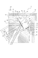
13 …光学箱
16 …板バネ(押圧部材;主規制部材)
20 …折返しミラー
24 …ストッパ(規制部;副規制部材)
28 …対向面(蓋に近い方の面)
90 …反射面
93 …稜線部(蓋側に一番近い稜線部)
Claims (7)
- 光源と、
前記光源から出射する光束を偏向する光偏向器と、
前記光偏向器が偏向した光束を所定面に反射させるミラーと、
前記ミラーを内包する光学箱と、
前記光学箱の座面に向って前記ミラーを押圧し、前記ミラーの反射面の法線方向における前記ミラーの動きを規制する押圧部材と、
前記光学箱の開口を塞ぐ蓋と、
を有し、前記光偏向器で偏向された光束で前記所定面を走査する走査光学装置において、
前記座面と平行な方向であり且つ前記蓋に近づく方向への前記ミラーの移動を規制する規制部が前記光学箱の一部に設けられており、
前記規制部は、前記法線方向に関して前記座面よりも前記ミラーがある側に突出する前記光学箱の部分であり、
前記押圧部材の全ての部分と前記規制部は、前記ミラーの複数の稜線のうち前記蓋に最も近い稜線よりも前記蓋から離れた領域に設けられていることを特徴とする走査光学装置。 - 前記光学箱は、前記ミラーの前記規制部に対向する面とは反対側の面が接触する第二の座面を有し、前記第二の座面に前記ミラーが接触している状態で前記ミラーと前記規制部の間には隙間があることを特徴とする請求項1に記載の走査光学装置。
- 前記隙間の距離δは、前記ミラーの副走査方向における有効反射長さをE、前記ミラーの反射面の前記副走査方向における前記光束の直径をDとした場合に、
δ<(E−D)/2
の条件を満たすように設定されていることを特徴とする請求項2に記載の走査光学装置。 - 光源と、
前記光源から出射する光束を偏向する光偏向器と、
前記光偏向器が偏向した光束を所定面に反射させるミラーと、
前記ミラーを内包する光学箱と、
前記光学箱の座面に向って前記ミラーを押圧し、前記ミラーの反射面の法線方向における前記ミラーの動きを規制する押圧部材と、
前記光学箱の開口を塞ぐ蓋と、
を有し、前記光偏向器で偏向された光束で前記所定面を走査する走査光学装置において、
前記座面と平行な方向であり且つ前記蓋に近づく方向へ前記ミラーを位置決めする基準部が前記光学箱の一部に設けられており、
前記基準部は、前記法線方向に関して前記座面よりも前記ミラーがある側に突出する前記光学箱の部分であり、
前記押圧部材の全ての部分と前記基準部は、前記ミラーの複数の稜線のうち前記蓋に最も近い稜線よりも前記蓋から離れた領域に設けられていることを特徴とする走査光学装置。 - 前記押圧部材を第一の押圧部材とすると、前記基準部に接触する前記ミラーの面とは反対側の面を前記基準部に向って押圧する第二の押圧部材を有することを特徴とする請求項4に記載の走査光学装置。
- 前記第一の押圧部材と前記第二の押圧部材は一体の部品であることを特徴とする請求項5に記載の走査光学装置。
- 請求項1〜6のいずれか1項に記載の走査光学装置を備えたことを特徴とする画像形成装置。
Priority Applications (3)
| Application Number | Priority Date | Filing Date | Title |
|---|---|---|---|
| JP2013015921A JP6108850B2 (ja) | 2013-01-30 | 2013-01-30 | 走査光学装置及びそれを備えた画像形成装置 |
| US14/167,633 US9411157B2 (en) | 2013-01-30 | 2014-01-29 | Optical scanning device, and image forming apparatus equipped with the same |
| US15/199,713 US9977237B2 (en) | 2013-01-30 | 2016-06-30 | Optical scanning device, and image forming apparatus equipped with the same |
Applications Claiming Priority (1)
| Application Number | Priority Date | Filing Date | Title |
|---|---|---|---|
| JP2013015921A JP6108850B2 (ja) | 2013-01-30 | 2013-01-30 | 走査光学装置及びそれを備えた画像形成装置 |
Related Child Applications (1)
| Application Number | Title | Priority Date | Filing Date |
|---|---|---|---|
| JP2017044176A Division JP6333430B2 (ja) | 2017-03-08 | 2017-03-08 | 走査光学装置及びそれを備えた画像形成装置 |
Publications (2)
| Publication Number | Publication Date |
|---|---|
| JP2014145998A JP2014145998A (ja) | 2014-08-14 |
| JP6108850B2 true JP6108850B2 (ja) | 2017-04-05 |
Family
ID=51222654
Family Applications (1)
| Application Number | Title | Priority Date | Filing Date |
|---|---|---|---|
| JP2013015921A Active JP6108850B2 (ja) | 2013-01-30 | 2013-01-30 | 走査光学装置及びそれを備えた画像形成装置 |
Country Status (2)
| Country | Link |
|---|---|
| US (2) | US9411157B2 (ja) |
| JP (1) | JP6108850B2 (ja) |
Families Citing this family (10)
| Publication number | Priority date | Publication date | Assignee | Title |
|---|---|---|---|---|
| JP6415067B2 (ja) * | 2014-03-26 | 2018-10-31 | キヤノン株式会社 | 光走査装置及び画像形成装置 |
| JP6739976B2 (ja) | 2016-04-19 | 2020-08-12 | キヤノン株式会社 | 光学走査装置及び画像形成装置 |
| JP2018055030A (ja) * | 2016-09-30 | 2018-04-05 | キヤノン株式会社 | 光走査装置及び画像形成装置 |
| JP6869046B2 (ja) * | 2017-02-17 | 2021-05-12 | シャープ株式会社 | 光走査装置および画像形成装置 |
| JP7163664B2 (ja) * | 2018-08-17 | 2022-11-01 | 京セラドキュメントソリューションズ株式会社 | 光偏向装置、光偏向装置を備えた光走査装置、及び光走査装置を備えた画像形成装置 |
| US11820158B2 (en) | 2018-10-19 | 2023-11-21 | Canon Kabushiki Kaisha | Image forming apparatus |
| US11108930B2 (en) * | 2019-03-13 | 2021-08-31 | Canon Kabushiki Kaisha | Image reading unit and image reading apparatus |
| CN110064847B (zh) * | 2019-04-22 | 2021-03-09 | 德玛克(长兴)注塑系统有限公司 | 一种跟踪式动态瓶盖打标方法 |
| JP7391566B2 (ja) | 2019-08-09 | 2023-12-05 | キヤノン株式会社 | 光走査装置およびそれを用いた画像形成装置 |
| JP7676222B2 (ja) * | 2021-05-24 | 2025-05-14 | キヤノン株式会社 | 走査光学装置及び画像形成装置 |
Family Cites Families (24)
| Publication number | Priority date | Publication date | Assignee | Title |
|---|---|---|---|---|
| JPH0844230A (ja) | 1994-07-28 | 1996-02-16 | Canon Inc | 定着装置 |
| JPH08254912A (ja) | 1995-03-17 | 1996-10-01 | Canon Inc | 定着装置及び画像形成装置 |
| JP3584131B2 (ja) * | 1996-09-13 | 2004-11-04 | キヤノン株式会社 | 光走査装置 |
| JPH10246862A (ja) | 1997-03-06 | 1998-09-14 | Canon Inc | 走査光学装置 |
| JP3984696B2 (ja) | 1998-01-30 | 2007-10-03 | キヤノン株式会社 | 画像形成装置および画像形成方法 |
| JP2001166241A (ja) | 1999-12-10 | 2001-06-22 | Canon Inc | 偏向走査装置 |
| JP3899768B2 (ja) | 2000-02-01 | 2007-03-28 | 富士ゼロックス株式会社 | 光学走査装置 |
| EP1184745B1 (en) | 2000-08-31 | 2010-11-17 | Ricoh Company, Ltd. | Electrophotographic image forming system |
| JP4516198B2 (ja) | 2000-08-31 | 2010-08-04 | 株式会社リコー | 電子写真画像形成装置 |
| JP2004021138A (ja) | 2002-06-20 | 2004-01-22 | Canon Inc | 画像形成装置および光走査装置 |
| JP4520231B2 (ja) * | 2004-06-30 | 2010-08-04 | 株式会社リコー | ミラー取り付け構造及び該取り付け構造を備えた光走査装置 |
| JP4557825B2 (ja) | 2004-07-21 | 2010-10-06 | キヤノン株式会社 | 画像形成装置 |
| JP4845448B2 (ja) | 2004-08-05 | 2011-12-28 | キヤノン株式会社 | 光学走査装置 |
| JP4502121B2 (ja) * | 2004-09-27 | 2010-07-14 | ブラザー工業株式会社 | 画像形成装置、カラー画像形成装置、走査ユニット及び走査レンズ |
| KR100644668B1 (ko) | 2004-12-18 | 2006-11-10 | 삼성전자주식회사 | 미러 지지 장치 및 이를 구비하는 광주사장치 |
| JP4689284B2 (ja) * | 2005-01-21 | 2011-05-25 | 株式会社リコー | 光走査装置および画像形成装置 |
| JP2007003726A (ja) | 2005-06-22 | 2007-01-11 | Canon Inc | 走査光学装置及び画像形成装置 |
| JP4965860B2 (ja) | 2006-01-18 | 2012-07-04 | キヤノン株式会社 | 光学走査装置 |
| JP4728312B2 (ja) | 2007-11-21 | 2011-07-20 | ブラザー工業株式会社 | 画像形成装置 |
| JP2010039155A (ja) * | 2008-08-05 | 2010-02-18 | Kyocera Mita Corp | 光走査装置及びこれを搭載した画像形成装置 |
| JP5153586B2 (ja) * | 2008-11-12 | 2013-02-27 | キヤノン株式会社 | 光学走査装置 |
| US8319813B2 (en) * | 2009-08-03 | 2012-11-27 | Lexmark International Inc. | Mounting assembly for reflection mirror in laser scanning unit |
| JP5614052B2 (ja) | 2010-02-22 | 2014-10-29 | 株式会社リコー | 光走査装置及び画像形成装置 |
| KR101873035B1 (ko) | 2012-01-11 | 2018-07-02 | 에이치피프린팅코리아 주식회사 | 광주사장치 및 이를 채용한 화상형성장치 |
-
2013
- 2013-01-30 JP JP2013015921A patent/JP6108850B2/ja active Active
-
2014
- 2014-01-29 US US14/167,633 patent/US9411157B2/en active Active
-
2016
- 2016-06-30 US US15/199,713 patent/US9977237B2/en active Active
Also Published As
| Publication number | Publication date |
|---|---|
| US9411157B2 (en) | 2016-08-09 |
| US20140211288A1 (en) | 2014-07-31 |
| JP2014145998A (ja) | 2014-08-14 |
| US20160313554A1 (en) | 2016-10-27 |
| US9977237B2 (en) | 2018-05-22 |
Similar Documents
| Publication | Publication Date | Title |
|---|---|---|
| JP2014145998A (ja) | 走査光学装置及びそれを備えた画像形成装置 | |
| KR101003004B1 (ko) | 광주사 장치 및 그것을 이용한 화상 형성 장치 | |
| US9268131B2 (en) | Optical scanning device and image forming apparatus including the same | |
| JP5219549B2 (ja) | 光走査装置 | |
| US20240337965A1 (en) | Optical scanning device and image forming apparatus | |
| JP6333430B2 (ja) | 走査光学装置及びそれを備えた画像形成装置 | |
| JP6541831B2 (ja) | 走査光学装置及びそれを備えた画像形成装置 | |
| US9380184B2 (en) | Optical scanning device and image forming apparatus therewith | |
| JP6061510B2 (ja) | 光走査装置、及びそれを備えた画像形成装置 | |
| JP7676222B2 (ja) | 走査光学装置及び画像形成装置 | |
| EP1762392B1 (en) | An image forming apparatus capable of producing a high-precision light beam | |
| JP6618257B2 (ja) | 光走査装置及び画像形成装置 | |
| US11108930B2 (en) | Image reading unit and image reading apparatus | |
| JP6016645B2 (ja) | 光走査装置、及びそれを備えた画像形成装置 | |
| US11997241B2 (en) | Optical scanning device and image forming apparatus including optical scanning device | |
| JP6547965B2 (ja) | 光走査装置及び該光走査装置を備えた画像形成装置 | |
| JP2010061110A (ja) | 光走査光学装置、該光走査光学装置を用いた画像形成装置並びに光走査方法 | |
| JP2011154118A (ja) | 光走査光学装置及び該光走査光学装置を用いた画像形成装置 | |
| JP5219267B2 (ja) | スキュー調整機構、光走査ユニット、および画像形成装置 | |
| JP2017159538A (ja) | 画像形成装置 | |
| JP6659123B2 (ja) | 走査光学装置及び画像形成装置 | |
| JP6624906B2 (ja) | 走査光学装置及び画像形成装置 | |
| JP6410049B2 (ja) | 光走査装置及び該光走査装置を備えた画像形成装置 | |
| JP6332075B2 (ja) | 光走査装置及び画像形成装置 | |
| JP2023007013A (ja) | 光走査装置及びそれを備えた画像形成装置 |
Legal Events
| Date | Code | Title | Description |
|---|---|---|---|
| A621 | Written request for application examination |
Free format text: JAPANESE INTERMEDIATE CODE: A621 Effective date: 20160120 |
|
| A977 | Report on retrieval |
Free format text: JAPANESE INTERMEDIATE CODE: A971007 Effective date: 20161018 |
|
| A131 | Notification of reasons for refusal |
Free format text: JAPANESE INTERMEDIATE CODE: A131 Effective date: 20161025 |
|
| A521 | Written amendment |
Free format text: JAPANESE INTERMEDIATE CODE: A523 Effective date: 20161220 |
|
| TRDD | Decision of grant or rejection written | ||
| A01 | Written decision to grant a patent or to grant a registration (utility model) |
Free format text: JAPANESE INTERMEDIATE CODE: A01 Effective date: 20170207 |
|
| A61 | First payment of annual fees (during grant procedure) |
Free format text: JAPANESE INTERMEDIATE CODE: A61 Effective date: 20170307 |
|
| R151 | Written notification of patent or utility model registration |
Ref document number: 6108850 Country of ref document: JP Free format text: JAPANESE INTERMEDIATE CODE: R151 |