JP5877992B2 - 表示装置 - Google Patents
表示装置 Download PDFInfo
- Publication number
- JP5877992B2 JP5877992B2 JP2011229456A JP2011229456A JP5877992B2 JP 5877992 B2 JP5877992 B2 JP 5877992B2 JP 2011229456 A JP2011229456 A JP 2011229456A JP 2011229456 A JP2011229456 A JP 2011229456A JP 5877992 B2 JP5877992 B2 JP 5877992B2
- Authority
- JP
- Japan
- Prior art keywords
- light
- layer
- liquid crystal
- substrate
- display device
- Prior art date
- Legal status (The legal status is an assumption and is not a legal conclusion. Google has not performed a legal analysis and makes no representation as to the accuracy of the status listed.)
- Expired - Fee Related
Links
Images


Classifications
-
- H—ELECTRICITY
- H10—SEMICONDUCTOR DEVICES; ELECTRIC SOLID-STATE DEVICES NOT OTHERWISE PROVIDED FOR
- H10H—INORGANIC LIGHT-EMITTING SEMICONDUCTOR DEVICES HAVING POTENTIAL BARRIERS
- H10H20/00—Individual inorganic light-emitting semiconductor devices having potential barriers, e.g. light-emitting diodes [LED]
- H10H20/80—Constructional details
- H10H20/85—Packages
- H10H20/851—Wavelength conversion means
- H10H20/8514—Wavelength conversion means characterised by their shape, e.g. plate or foil
-
- H—ELECTRICITY
- H10—SEMICONDUCTOR DEVICES; ELECTRIC SOLID-STATE DEVICES NOT OTHERWISE PROVIDED FOR
- H10H—INORGANIC LIGHT-EMITTING SEMICONDUCTOR DEVICES HAVING POTENTIAL BARRIERS
- H10H20/00—Individual inorganic light-emitting semiconductor devices having potential barriers, e.g. light-emitting diodes [LED]
- H10H20/80—Constructional details
- H10H20/85—Packages
- H10H20/855—Optical field-shaping means, e.g. lenses
- H10H20/856—Reflecting means
-
- G—PHYSICS
- G02—OPTICS
- G02F—OPTICAL DEVICES OR ARRANGEMENTS FOR THE CONTROL OF LIGHT BY MODIFICATION OF THE OPTICAL PROPERTIES OF THE MEDIA OF THE ELEMENTS INVOLVED THEREIN; NON-LINEAR OPTICS; FREQUENCY-CHANGING OF LIGHT; OPTICAL LOGIC ELEMENTS; OPTICAL ANALOGUE/DIGITAL CONVERTERS
- G02F1/00—Devices or arrangements for the control of the intensity, colour, phase, polarisation or direction of light arriving from an independent light source, e.g. switching, gating or modulating; Non-linear optics
- G02F1/01—Devices or arrangements for the control of the intensity, colour, phase, polarisation or direction of light arriving from an independent light source, e.g. switching, gating or modulating; Non-linear optics for the control of the intensity, phase, polarisation or colour
- G02F1/13—Devices or arrangements for the control of the intensity, colour, phase, polarisation or direction of light arriving from an independent light source, e.g. switching, gating or modulating; Non-linear optics for the control of the intensity, phase, polarisation or colour based on liquid crystals, e.g. single liquid crystal display cells
- G02F1/133—Constructional arrangements; Operation of liquid crystal cells; Circuit arrangements
- G02F1/1333—Constructional arrangements; Manufacturing methods
- G02F1/1335—Structural association of cells with optical devices, e.g. polarisers or reflectors
- G02F1/133509—Filters, e.g. light shielding masks
- G02F1/133514—Colour filters
-
- G—PHYSICS
- G02—OPTICS
- G02F—OPTICAL DEVICES OR ARRANGEMENTS FOR THE CONTROL OF LIGHT BY MODIFICATION OF THE OPTICAL PROPERTIES OF THE MEDIA OF THE ELEMENTS INVOLVED THEREIN; NON-LINEAR OPTICS; FREQUENCY-CHANGING OF LIGHT; OPTICAL LOGIC ELEMENTS; OPTICAL ANALOGUE/DIGITAL CONVERTERS
- G02F1/00—Devices or arrangements for the control of the intensity, colour, phase, polarisation or direction of light arriving from an independent light source, e.g. switching, gating or modulating; Non-linear optics
- G02F1/01—Devices or arrangements for the control of the intensity, colour, phase, polarisation or direction of light arriving from an independent light source, e.g. switching, gating or modulating; Non-linear optics for the control of the intensity, phase, polarisation or colour
- G02F1/13—Devices or arrangements for the control of the intensity, colour, phase, polarisation or direction of light arriving from an independent light source, e.g. switching, gating or modulating; Non-linear optics for the control of the intensity, phase, polarisation or colour based on liquid crystals, e.g. single liquid crystal display cells
- G02F1/133—Constructional arrangements; Operation of liquid crystal cells; Circuit arrangements
- G02F1/1333—Constructional arrangements; Manufacturing methods
- G02F1/1335—Structural association of cells with optical devices, e.g. polarisers or reflectors
- G02F1/1336—Illuminating devices
- G02F1/133602—Direct backlight
- G02F1/133603—Direct backlight with LEDs
-
- G—PHYSICS
- G02—OPTICS
- G02F—OPTICAL DEVICES OR ARRANGEMENTS FOR THE CONTROL OF LIGHT BY MODIFICATION OF THE OPTICAL PROPERTIES OF THE MEDIA OF THE ELEMENTS INVOLVED THEREIN; NON-LINEAR OPTICS; FREQUENCY-CHANGING OF LIGHT; OPTICAL LOGIC ELEMENTS; OPTICAL ANALOGUE/DIGITAL CONVERTERS
- G02F1/00—Devices or arrangements for the control of the intensity, colour, phase, polarisation or direction of light arriving from an independent light source, e.g. switching, gating or modulating; Non-linear optics
- G02F1/01—Devices or arrangements for the control of the intensity, colour, phase, polarisation or direction of light arriving from an independent light source, e.g. switching, gating or modulating; Non-linear optics for the control of the intensity, phase, polarisation or colour
- G02F1/13—Devices or arrangements for the control of the intensity, colour, phase, polarisation or direction of light arriving from an independent light source, e.g. switching, gating or modulating; Non-linear optics for the control of the intensity, phase, polarisation or colour based on liquid crystals, e.g. single liquid crystal display cells
- G02F1/133—Constructional arrangements; Operation of liquid crystal cells; Circuit arrangements
- G02F1/1333—Constructional arrangements; Manufacturing methods
- G02F1/1335—Structural association of cells with optical devices, e.g. polarisers or reflectors
- G02F1/1336—Illuminating devices
- G02F1/133621—Illuminating devices providing coloured light
-
- H—ELECTRICITY
- H10—SEMICONDUCTOR DEVICES; ELECTRIC SOLID-STATE DEVICES NOT OTHERWISE PROVIDED FOR
- H10H—INORGANIC LIGHT-EMITTING SEMICONDUCTOR DEVICES HAVING POTENTIAL BARRIERS
- H10H20/00—Individual inorganic light-emitting semiconductor devices having potential barriers, e.g. light-emitting diodes [LED]
- H10H20/80—Constructional details
- H10H20/85—Packages
- H10H20/851—Wavelength conversion means
-
- H—ELECTRICITY
- H10—SEMICONDUCTOR DEVICES; ELECTRIC SOLID-STATE DEVICES NOT OTHERWISE PROVIDED FOR
- H10H—INORGANIC LIGHT-EMITTING SEMICONDUCTOR DEVICES HAVING POTENTIAL BARRIERS
- H10H20/00—Individual inorganic light-emitting semiconductor devices having potential barriers, e.g. light-emitting diodes [LED]
- H10H20/80—Constructional details
- H10H20/85—Packages
- H10H20/852—Encapsulations
- H10H20/853—Encapsulations characterised by their shape
-
- H—ELECTRICITY
- H10—SEMICONDUCTOR DEVICES; ELECTRIC SOLID-STATE DEVICES NOT OTHERWISE PROVIDED FOR
- H10H—INORGANIC LIGHT-EMITTING SEMICONDUCTOR DEVICES HAVING POTENTIAL BARRIERS
- H10H20/00—Individual inorganic light-emitting semiconductor devices having potential barriers, e.g. light-emitting diodes [LED]
- H10H20/80—Constructional details
- H10H20/85—Packages
- H10H20/852—Encapsulations
- H10H20/854—Encapsulations characterised by their material, e.g. epoxy or silicone resins
-
- H—ELECTRICITY
- H10—SEMICONDUCTOR DEVICES; ELECTRIC SOLID-STATE DEVICES NOT OTHERWISE PROVIDED FOR
- H10H—INORGANIC LIGHT-EMITTING SEMICONDUCTOR DEVICES HAVING POTENTIAL BARRIERS
- H10H20/00—Individual inorganic light-emitting semiconductor devices having potential barriers, e.g. light-emitting diodes [LED]
- H10H20/80—Constructional details
- H10H20/85—Packages
- H10H20/857—Interconnections, e.g. lead-frames, bond wires or solder balls
-
- H—ELECTRICITY
- H10—SEMICONDUCTOR DEVICES; ELECTRIC SOLID-STATE DEVICES NOT OTHERWISE PROVIDED FOR
- H10H—INORGANIC LIGHT-EMITTING SEMICONDUCTOR DEVICES HAVING POTENTIAL BARRIERS
- H10H20/00—Individual inorganic light-emitting semiconductor devices having potential barriers, e.g. light-emitting diodes [LED]
- H10H20/80—Constructional details
- H10H20/862—Resonant cavity structures
-
- H—ELECTRICITY
- H10—SEMICONDUCTOR DEVICES; ELECTRIC SOLID-STATE DEVICES NOT OTHERWISE PROVIDED FOR
- H10W—GENERIC PACKAGES, INTERCONNECTIONS, CONNECTORS OR OTHER CONSTRUCTIONAL DETAILS OF DEVICES COVERED BY CLASS H10
- H10W90/00—Package configurations
-
- H—ELECTRICITY
- H10—SEMICONDUCTOR DEVICES; ELECTRIC SOLID-STATE DEVICES NOT OTHERWISE PROVIDED FOR
- H10H—INORGANIC LIGHT-EMITTING SEMICONDUCTOR DEVICES HAVING POTENTIAL BARRIERS
- H10H20/00—Individual inorganic light-emitting semiconductor devices having potential barriers, e.g. light-emitting diodes [LED]
- H10H20/80—Constructional details
- H10H20/85—Packages
- H10H20/8506—Containers
-
- H—ELECTRICITY
- H10—SEMICONDUCTOR DEVICES; ELECTRIC SOLID-STATE DEVICES NOT OTHERWISE PROVIDED FOR
- H10W—GENERIC PACKAGES, INTERCONNECTIONS, CONNECTORS OR OTHER CONSTRUCTIONAL DETAILS OF DEVICES COVERED BY CLASS H10
- H10W72/00—Interconnections or connectors in packages
- H10W72/50—Bond wires
- H10W72/531—Shapes of wire connectors
- H10W72/536—Shapes of wire connectors the connected ends being ball-shaped
-
- H—ELECTRICITY
- H10—SEMICONDUCTOR DEVICES; ELECTRIC SOLID-STATE DEVICES NOT OTHERWISE PROVIDED FOR
- H10W—GENERIC PACKAGES, INTERCONNECTIONS, CONNECTORS OR OTHER CONSTRUCTIONAL DETAILS OF DEVICES COVERED BY CLASS H10
- H10W72/00—Interconnections or connectors in packages
- H10W72/50—Bond wires
- H10W72/531—Shapes of wire connectors
- H10W72/5363—Shapes of wire connectors the connected ends being wedge-shaped
-
- H—ELECTRICITY
- H10—SEMICONDUCTOR DEVICES; ELECTRIC SOLID-STATE DEVICES NOT OTHERWISE PROVIDED FOR
- H10W—GENERIC PACKAGES, INTERCONNECTIONS, CONNECTORS OR OTHER CONSTRUCTIONAL DETAILS OF DEVICES COVERED BY CLASS H10
- H10W90/00—Package configurations
- H10W90/701—Package configurations characterised by the relative positions of pads or connectors relative to package parts
- H10W90/751—Package configurations characterised by the relative positions of pads or connectors relative to package parts of bond wires
- H10W90/754—Package configurations characterised by the relative positions of pads or connectors relative to package parts of bond wires between a chip and a stacked insulating package substrate, interposer or RDL
Landscapes
- Physics & Mathematics (AREA)
- Nonlinear Science (AREA)
- Optics & Photonics (AREA)
- Crystallography & Structural Chemistry (AREA)
- Chemical & Material Sciences (AREA)
- General Physics & Mathematics (AREA)
- Mathematical Physics (AREA)
- Led Device Packages (AREA)
- Liquid Crystal (AREA)
- Planar Illumination Modules (AREA)
- Devices For Indicating Variable Information By Combining Individual Elements (AREA)
- Fastening Of Light Sources Or Lamp Holders (AREA)
- Mechanical Light Control Or Optical Switches (AREA)
Description
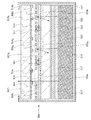
本実施の形態では、消費電力を低減することが可能な、LEDユニット及びバックライトについて、図1及び図2を用いて説明する。
なお、nは、透光性を有する層51の屈折率を示す。
本実施の形態では、実施の形態1で説明したバックライトモジュールを用いた液晶表示装置について説明する。
本実施の形態では、MEMS(Micro Electro Mechanical Systems)を用いて各画素におけるバックライトからの光の透過量を制御する表示装置について、図12乃至図14を用いて説明する。
本発明の一態様である表示装置は、さまざまな電子機器に適用することができる。電子機器としては、例えば、テレビジョン装置(テレビ、またはテレビジョン受信機ともいう)などが挙げられる。さらには、屋内でのデジタルサイネージ(Digital Signage:電子看板)、PID(Public Information Display)、電車などの乗り物の車内広告等に適用することができる。特に、本発明の一態様である表示装置は、色純度を向上させることができることため、本発明の一態様である表示装置を、色再現性を求められる上記電子機器として用いることは有用である。そこで、本発明の一態様である表示装置を用いた電子機器の一例を、図15に示す。
Claims (3)
- バックライトモジュールと、
前記バックライトモジュールと重なる領域を有する、散乱板と、
前記散乱板と重なる領域を有する、第1の偏光板と、
前記第1の偏光板と重なる領域を有する、液晶パネルと、
前記液晶パネルと重なる領域を有する、第2の偏光板と、を有し、
前記バックライトモジュールは、第1の基板と、発光素子ユニットとを有し、
前記発光素子ユニットは、
第2の基板と、
前記第2の基板上に配置された、発光素子チップと、微小光共振器と、
前記発光素子チップと、前記微小光共振器と、を覆う蛍光体層と、を有し、
前記微小光共振器は、
反射層と、
前記反射層上の、透光性を有する層と、
前記透光性を有する層上の、半透過型反射層と、を有し、
前記微小光共振器は、前記発光素子チップの周辺に配置され、
前記微小光共振器は、前記反射層と前記半透過型反射層との間で反射し干渉させた光を射出し、
前記微小光共振器は、特定の発光スペクトルの波長の強度を高める機能を有することを特徴とする表示装置。 - 請求項1において、
前記半透過型反射層は、前記透光性を有する層の上面及び側壁を覆うことを特徴とする表示装置。 - 請求項1又は請求項2において、
前記第1の基板と対向した、第3の基板を有し、
前記液晶パネルは、前記第3の基板側に、着色層を有することを特徴とする表示装置。
Priority Applications (1)
| Application Number | Priority Date | Filing Date | Title |
|---|---|---|---|
| JP2011229456A JP5877992B2 (ja) | 2010-10-25 | 2011-10-19 | 表示装置 |
Applications Claiming Priority (3)
| Application Number | Priority Date | Filing Date | Title |
|---|---|---|---|
| JP2010238723 | 2010-10-25 | ||
| JP2010238723 | 2010-10-25 | ||
| JP2011229456A JP5877992B2 (ja) | 2010-10-25 | 2011-10-19 | 表示装置 |
Related Child Applications (1)
| Application Number | Title | Priority Date | Filing Date |
|---|---|---|---|
| JP2016012963A Division JP6134400B2 (ja) | 2010-10-25 | 2016-01-27 | 表示装置 |
Publications (3)
| Publication Number | Publication Date |
|---|---|
| JP2012109549A JP2012109549A (ja) | 2012-06-07 |
| JP2012109549A5 JP2012109549A5 (ja) | 2014-10-16 |
| JP5877992B2 true JP5877992B2 (ja) | 2016-03-08 |
Family
ID=45972748
Family Applications (3)
| Application Number | Title | Priority Date | Filing Date |
|---|---|---|---|
| JP2011229456A Expired - Fee Related JP5877992B2 (ja) | 2010-10-25 | 2011-10-19 | 表示装置 |
| JP2016012963A Expired - Fee Related JP6134400B2 (ja) | 2010-10-25 | 2016-01-27 | 表示装置 |
| JP2017084377A Expired - Fee Related JP6371437B2 (ja) | 2010-10-25 | 2017-04-21 | 発光素子ユニット |
Family Applications After (2)
| Application Number | Title | Priority Date | Filing Date |
|---|---|---|---|
| JP2016012963A Expired - Fee Related JP6134400B2 (ja) | 2010-10-25 | 2016-01-27 | 表示装置 |
| JP2017084377A Expired - Fee Related JP6371437B2 (ja) | 2010-10-25 | 2017-04-21 | 発光素子ユニット |
Country Status (3)
| Country | Link |
|---|---|
| US (2) | US9306129B2 (ja) |
| JP (3) | JP5877992B2 (ja) |
| KR (1) | KR20120042691A (ja) |
Cited By (1)
| Publication number | Priority date | Publication date | Assignee | Title |
|---|---|---|---|---|
| JP2017168851A (ja) * | 2010-10-25 | 2017-09-21 | 株式会社半導体エネルギー研究所 | 発光素子ユニット |
Families Citing this family (29)
| Publication number | Priority date | Publication date | Assignee | Title |
|---|---|---|---|---|
| US8953120B2 (en) | 2011-01-07 | 2015-02-10 | Semiconductor Energy Laboratory Co., Ltd. | Display device |
| KR20120112896A (ko) * | 2011-04-04 | 2012-10-12 | 삼성디스플레이 주식회사 | 백라이트 어셈블리, 이의 제조 방법 및 이를 포함하는 표시 장치 |
| US9711110B2 (en) | 2012-04-06 | 2017-07-18 | Semiconductor Energy Laboratory Co., Ltd. | Display device comprising grayscale conversion portion and display portion |
| US9793444B2 (en) * | 2012-04-06 | 2017-10-17 | Semiconductor Energy Laboratory Co., Ltd. | Display device and electronic device |
| TWI588540B (zh) | 2012-05-09 | 2017-06-21 | 半導體能源研究所股份有限公司 | 顯示裝置和電子裝置 |
| TWI675222B (zh) | 2012-05-09 | 2019-10-21 | 日商半導體能源研究所股份有限公司 | 驅動半導體裝置的方法 |
| KR102135352B1 (ko) * | 2013-08-20 | 2020-07-17 | 엘지전자 주식회사 | 표시장치 |
| JP2015118272A (ja) * | 2013-12-18 | 2015-06-25 | 株式会社 オルタステクノロジー | ヘッドアップディスプレイ装置用液晶表示装置及びヘッドアップディスプレイ装置 |
| US9541794B2 (en) | 2014-01-10 | 2017-01-10 | Apple Inc. | High dynamic range liquid crystal display |
| JP6250575B2 (ja) * | 2015-03-06 | 2017-12-20 | 富士フイルム株式会社 | バックライトユニットおよび画像表示装置 |
| KR102373329B1 (ko) * | 2015-04-30 | 2022-03-11 | 삼성디스플레이 주식회사 | 유기 발광 표시 장치 |
| KR102377794B1 (ko) * | 2015-07-06 | 2022-03-23 | 엘지전자 주식회사 | 반도체 발광 소자를 이용한 디스플레이 장치 및 이의 제조방법 |
| KR102396325B1 (ko) * | 2015-10-12 | 2022-05-13 | 삼성전자주식회사 | 엘이디 디스플레이 장치의 광학 부재 및 엘이디 디스플레이 장치 |
| TWI574087B (zh) * | 2016-06-21 | 2017-03-11 | 鴻海精密工業股份有限公司 | 光源模塊及背光模塊 |
| JP6837579B2 (ja) | 2018-01-12 | 2021-03-03 | 富士フイルム株式会社 | バックライトユニットおよび液晶表示装置 |
| KR102105125B1 (ko) * | 2018-06-27 | 2020-05-29 | 한국광기술원 | 이중 프린팅 배선 구조를 갖는 스트레처블 패치 및 이중 프린팅 배선 구조를 갖는 스트레처블 패치 제조방법 |
| CN109148505B (zh) * | 2018-08-23 | 2022-04-29 | 京东方科技集团股份有限公司 | 一种顶发射MircroLED显示面板及其制造方法 |
| CN110867507B (zh) * | 2018-08-28 | 2021-10-08 | 隆达电子股份有限公司 | 发光装置以及背光模块 |
| DE102018126113A1 (de) * | 2018-10-19 | 2020-04-23 | Osram Opto Semiconductors Gmbh | Farbige Leuchtzelle für bildgebende Einheit mit Primärfarbenauswahl dank oszillierendem Bauteil |
| KR102694329B1 (ko) * | 2018-12-10 | 2024-08-13 | 삼성전자주식회사 | 디스플레이 모듈, 이를 포함하는 디스플레이 장치 및 디스플레이 모듈 제조 방법 |
| KR102803995B1 (ko) * | 2019-04-03 | 2025-05-12 | 삼성디스플레이 주식회사 | 표시 장치 및 이의 제조 방법 |
| US11982905B2 (en) | 2020-05-22 | 2024-05-14 | Apple Inc. | Electronic device display with a backlight having light-emitting diodes and driver integrated circuits in an active area |
| US12074151B2 (en) * | 2020-06-03 | 2024-08-27 | Jade Bird Display (shanghai) Limited | Systems and methods for multi-color LED pixel unit with vertical light emission |
| TWI756061B (zh) * | 2021-02-22 | 2022-02-21 | 友達光電股份有限公司 | 顯示裝置 |
| CN113078190B (zh) * | 2021-03-19 | 2022-08-23 | 厦门天马微电子有限公司 | 显示面板及显示装置 |
| CN114156306B (zh) * | 2021-11-30 | 2023-07-25 | 深圳市华星光电半导体显示技术有限公司 | 显示面板的制作方法、显示面板以及显示装置 |
| CN118975414A (zh) * | 2022-03-30 | 2024-11-15 | 太阳控股株式会社 | 安装用基板、连接结构体、及电子部件 |
| TWI824770B (zh) | 2022-10-13 | 2023-12-01 | 財團法人工業技術研究院 | 顯示器元件與投影器 |
| CN119008814A (zh) * | 2024-08-13 | 2024-11-22 | 江西省鑫聚能科技有限公司 | 一种led芯片凸台载板及其生产方法和控制系统 |
Family Cites Families (63)
| Publication number | Priority date | Publication date | Assignee | Title |
|---|---|---|---|---|
| JPS60247622A (ja) | 1984-05-23 | 1985-12-07 | Oki Electric Ind Co Ltd | 液晶表示装置 |
| JPH01160063A (ja) * | 1987-12-16 | 1989-06-22 | Fujitsu Ltd | 発光素子 |
| JPH08262438A (ja) | 1995-03-23 | 1996-10-11 | Alps Electric Co Ltd | 液晶表示装置のバックライト構造 |
| JPH0992909A (ja) | 1995-09-21 | 1997-04-04 | Casio Comput Co Ltd | スイッチング素子、スイッチング素子の製造方法、およびスイッチング素子を用いた表示装置 |
| US5813753A (en) * | 1997-05-27 | 1998-09-29 | Philips Electronics North America Corporation | UV/blue led-phosphor device with efficient conversion of UV/blues light to visible light |
| US5813752A (en) * | 1997-05-27 | 1998-09-29 | Philips Electronics North America Corporation | UV/blue LED-phosphor device with short wave pass, long wave pass band pass and peroit filters |
| US6304304B1 (en) | 1997-11-20 | 2001-10-16 | Sanyo Electric Co., Ltd. | Liquid crystal display having an off driving voltage greater than either zero or an optical characteristics changing voltage |
| JP2004295141A (ja) | 1997-11-20 | 2004-10-21 | Sanyo Electric Co Ltd | 液晶表示装置 |
| JPH11174994A (ja) | 1997-12-11 | 1999-07-02 | Sharp Corp | 表示装置 |
| US6037719A (en) | 1998-04-09 | 2000-03-14 | Hughes Electronics Corporation | Matrix-addressed display having micromachined electromechanical switches |
| JP3865942B2 (ja) | 1998-07-17 | 2007-01-10 | 富士フイルムホールディングス株式会社 | アクティブマトリクス素子、及びアクティブマトリクス素子を用いた発光素子、光変調素子、光検出素子、露光素子、表示装置 |
| JP3590283B2 (ja) | 1999-01-13 | 2004-11-17 | 日本電信電話株式会社 | 静電型可動接点素子の製造方法 |
| TW459275B (en) | 1999-07-06 | 2001-10-11 | Semiconductor Energy Lab | Semiconductor device and method of fabricating the same |
| JP3185793B2 (ja) | 1999-07-19 | 2001-07-11 | 松下電器産業株式会社 | 液晶表示素子 |
| US6583915B1 (en) | 1999-10-08 | 2003-06-24 | Lg. Philips Lcd Co., Ltd. | Display device using a micro light modulator and fabricating method thereof |
| KR100634831B1 (ko) | 1999-12-04 | 2006-10-17 | 엘지.필립스 엘시디 주식회사 | 미세 광변조기를 이용한 투과형 표시소자 |
| JP2002082652A (ja) | 2000-05-18 | 2002-03-22 | Canon Inc | 画像表示装置および方法 |
| US6998281B2 (en) * | 2000-10-12 | 2006-02-14 | General Electric Company | Solid state lighting device with reduced form factor including LED with directional emission and package with microoptics |
| US20040031670A1 (en) | 2001-10-31 | 2004-02-19 | Wong Marvin Glenn | Method of actuating a high power micromachined switch |
| US20030080839A1 (en) | 2001-10-31 | 2003-05-01 | Wong Marvin Glenn | Method for improving the power handling capacity of MEMS switches |
| JP4164562B2 (ja) * | 2002-09-11 | 2008-10-15 | 独立行政法人科学技術振興機構 | ホモロガス薄膜を活性層として用いる透明薄膜電界効果型トランジスタ |
| US6657525B1 (en) | 2002-05-31 | 2003-12-02 | Northrop Grumman Corporation | Microelectromechanical RF switch |
| TWI351548B (en) | 2003-01-15 | 2011-11-01 | Semiconductor Energy Lab | Manufacturing method of liquid crystal display dev |
| JP4408044B2 (ja) | 2003-01-15 | 2010-02-03 | 株式会社半導体エネルギー研究所 | 液晶表示装置の作製方法 |
| US7502392B2 (en) | 2003-09-12 | 2009-03-10 | Semiconductor Energy Laboratory Co., Ltd. | Laser oscillator |
| EP1737044B1 (en) * | 2004-03-12 | 2014-12-10 | Japan Science and Technology Agency | Amorphous oxide and thin film transistor |
| JP4712413B2 (ja) | 2004-04-19 | 2011-06-29 | シチズンホールディングス株式会社 | 可変光減衰器およびそれを備えた光学フィルタ |
| JP2005311153A (ja) * | 2004-04-23 | 2005-11-04 | Harison Toshiba Lighting Corp | 発光素子の外囲器 |
| US7416977B2 (en) | 2004-04-28 | 2008-08-26 | Semiconductor Energy Laboratory Co., Ltd. | Method for manufacturing display device, liquid crystal television, and EL television |
| US7985677B2 (en) | 2004-11-30 | 2011-07-26 | Semiconductor Energy Laboratory Co., Ltd. | Method of manufacturing semiconductor device |
| EP2085807B1 (en) | 2005-02-23 | 2014-10-29 | Pixtronix, Inc. | Display methods and apparatus |
| KR100991044B1 (ko) * | 2005-02-23 | 2010-10-29 | 픽스트로닉스 인코포레이티드 | 디스플레이 장치들 및 그의 제조 방법들 |
| US7304785B2 (en) * | 2005-02-23 | 2007-12-04 | Pixtronix, Inc. | Display methods and apparatus |
| US7271945B2 (en) | 2005-02-23 | 2007-09-18 | Pixtronix, Inc. | Methods and apparatus for actuating displays |
| JP2006351808A (ja) * | 2005-06-15 | 2006-12-28 | Matsushita Electric Works Ltd | 発光装置 |
| TWI261378B (en) * | 2005-09-19 | 2006-09-01 | Ind Tech Res Inst | Polarized light emitting device |
| DE102005062514A1 (de) * | 2005-09-28 | 2007-03-29 | Osram Opto Semiconductors Gmbh | Optoelektronisches Bauelement |
| US8043950B2 (en) | 2005-10-26 | 2011-10-25 | Semiconductor Energy Laboratory Co., Ltd. | Semiconductor device and manufacturing method thereof |
| JP2007165029A (ja) * | 2005-12-12 | 2007-06-28 | Hitachi Displays Ltd | 表示装置 |
| JP2007180329A (ja) * | 2005-12-28 | 2007-07-12 | Toshiba Lighting & Technology Corp | 発光ダイオード照明装置 |
| US7741687B2 (en) | 2006-03-10 | 2010-06-22 | Semiconductor Energy Laboratory Co., Ltd. | Microstructure, semiconductor device, and manufacturing method of the microstructure |
| JP2007273562A (ja) | 2006-03-30 | 2007-10-18 | Toshiba Corp | 半導体発光装置 |
| JP2007279480A (ja) | 2006-04-10 | 2007-10-25 | Hitachi Displays Ltd | 液晶表示装置 |
| CN101405215B (zh) | 2006-05-18 | 2013-01-09 | 株式会社半导体能源研究所 | 微结构、微机械、以及微结构和微机械的制造方法 |
| US7876489B2 (en) | 2006-06-05 | 2011-01-25 | Pixtronix, Inc. | Display apparatus with optical cavities |
| JP2008004645A (ja) * | 2006-06-20 | 2008-01-10 | Harison Toshiba Lighting Corp | 発光デバイス |
| WO2008025723A1 (en) * | 2006-08-29 | 2008-03-06 | Osram Sylvania Inc. | Enhanced emission from phosphor-converted leds using interferometric filters |
| JP5421121B2 (ja) * | 2007-01-19 | 2014-02-19 | ピクストロニクス,インコーポレイテッド | Memsディスプレイ装置 |
| CN101271869B (zh) * | 2007-03-22 | 2015-11-25 | 株式会社半导体能源研究所 | 发光器件的制造方法 |
| EP1976015B1 (en) | 2007-03-26 | 2014-09-10 | Semiconductor Energy Laboratory Co., Ltd. | Switching element, method for manufacturing the same, and display device including switching element |
| DE102008012316B4 (de) * | 2007-09-28 | 2023-02-02 | OSRAM Opto Semiconductors Gesellschaft mit beschränkter Haftung | Halbleiterlichtquelle mit einer Primärstrahlungsquelle und einem Lumineszenzkonversionselement |
| JP5210901B2 (ja) | 2008-02-06 | 2013-06-12 | 株式会社半導体エネルギー研究所 | 液晶表示装置 |
| JP2009224245A (ja) * | 2008-03-18 | 2009-10-01 | Sony Corp | 発光装置および液晶表示装置 |
| CN102007608B (zh) | 2008-05-27 | 2012-11-14 | 夏普株式会社 | Led光源装置、背光装置以及液晶显示装置 |
| JP2010040976A (ja) * | 2008-08-08 | 2010-02-18 | Sony Corp | 発光素子及びこれを用いた照明装置並びに表示装置 |
| JP2010062067A (ja) * | 2008-09-05 | 2010-03-18 | Sony Corp | 表示装置の製造方法および表示装置 |
| JP5238826B2 (ja) | 2009-01-27 | 2013-07-17 | シャープ株式会社 | 液晶表示装置 |
| US8461582B2 (en) * | 2009-03-05 | 2013-06-11 | Semiconductor Energy Laboratory Co., Ltd. | Semiconductor device and method for manufacturing the same |
| WO2011025173A2 (en) | 2009-08-27 | 2011-03-03 | Lg Electronics Inc. | Backlight unit and display device |
| JP2011059149A (ja) | 2009-09-07 | 2011-03-24 | Hitachi Displays Ltd | 電子機器 |
| TWI531088B (zh) * | 2009-11-13 | 2016-04-21 | 首爾偉傲世有限公司 | 具有分散式布拉格反射器的發光二極體晶片 |
| JP2012033633A (ja) * | 2010-07-29 | 2012-02-16 | Fujifilm Corp | 発光装置 |
| JP5877992B2 (ja) * | 2010-10-25 | 2016-03-08 | 株式会社半導体エネルギー研究所 | 表示装置 |
-
2011
- 2011-10-19 JP JP2011229456A patent/JP5877992B2/ja not_active Expired - Fee Related
- 2011-10-20 US US13/277,417 patent/US9306129B2/en not_active Expired - Fee Related
- 2011-10-24 KR KR1020110108651A patent/KR20120042691A/ko not_active Ceased
-
2016
- 2016-01-27 JP JP2016012963A patent/JP6134400B2/ja not_active Expired - Fee Related
- 2016-04-01 US US15/088,174 patent/US20160218258A1/en not_active Abandoned
-
2017
- 2017-04-21 JP JP2017084377A patent/JP6371437B2/ja not_active Expired - Fee Related
Cited By (1)
| Publication number | Priority date | Publication date | Assignee | Title |
|---|---|---|---|---|
| JP2017168851A (ja) * | 2010-10-25 | 2017-09-21 | 株式会社半導体エネルギー研究所 | 発光素子ユニット |
Also Published As
| Publication number | Publication date |
|---|---|
| US20160218258A1 (en) | 2016-07-28 |
| JP2017168851A (ja) | 2017-09-21 |
| US9306129B2 (en) | 2016-04-05 |
| KR20120042691A (ko) | 2012-05-03 |
| JP2016075959A (ja) | 2016-05-12 |
| JP6371437B2 (ja) | 2018-08-08 |
| JP6134400B2 (ja) | 2017-05-24 |
| JP2012109549A (ja) | 2012-06-07 |
| US20120099048A1 (en) | 2012-04-26 |
Similar Documents
| Publication | Publication Date | Title |
|---|---|---|
| JP5877992B2 (ja) | 表示装置 | |
| US8891051B2 (en) | Backlight and display device | |
| US12197064B2 (en) | Liquid crystal display and manufacturing method thereof | |
| TWI522708B (zh) | 液晶顯示裝置 | |
| TWI616707B (zh) | 液晶顯示裝置 | |
| TWI438529B (zh) | 顯示裝置 | |
| TWI529465B (zh) | 液晶顯示裝置 | |
| CN101676783A (zh) | 薄膜晶体管显示面板、液晶显示器及其制造方法 | |
| KR20100088535A (ko) | 액정 표시 장치 | |
| US10120234B2 (en) | Liquid crystal display apparatus | |
| WO2018147279A1 (ja) | 反射偏光層、波長変換層及び液晶表示装置 | |
| TWI831207B (zh) | 電子裝置 | |
| US9459491B2 (en) | Mirror display device and manufacturing method thereof | |
| JP2007206557A (ja) | 液晶表示装置 | |
| JP2007052369A (ja) | 液晶表示装置 | |
| KR20150106029A (ko) | 백라이트 어셈블리 및 이를 포함하는 표시 장치 | |
| CN112703554B (zh) | 显示装置及电子设备 | |
| WO2013005644A1 (ja) | 表示装置 | |
| US12523897B2 (en) | Electronic device | |
| JP7407585B2 (ja) | 液晶表示装置 |
Legal Events
| Date | Code | Title | Description |
|---|---|---|---|
| A521 | Request for written amendment filed |
Free format text: JAPANESE INTERMEDIATE CODE: A523 Effective date: 20140829 |
|
| A621 | Written request for application examination |
Free format text: JAPANESE INTERMEDIATE CODE: A621 Effective date: 20140829 |
|
| A977 | Report on retrieval |
Free format text: JAPANESE INTERMEDIATE CODE: A971007 Effective date: 20150529 |
|
| A131 | Notification of reasons for refusal |
Free format text: JAPANESE INTERMEDIATE CODE: A131 Effective date: 20150609 |
|
| A521 | Request for written amendment filed |
Free format text: JAPANESE INTERMEDIATE CODE: A523 Effective date: 20150803 |
|
| TRDD | Decision of grant or rejection written | ||
| A01 | Written decision to grant a patent or to grant a registration (utility model) |
Free format text: JAPANESE INTERMEDIATE CODE: A01 Effective date: 20160119 |
|
| A61 | First payment of annual fees (during grant procedure) |
Free format text: JAPANESE INTERMEDIATE CODE: A61 Effective date: 20160127 |
|
| R150 | Certificate of patent or registration of utility model |
Ref document number: 5877992 Country of ref document: JP Free format text: JAPANESE INTERMEDIATE CODE: R150 |
|
| R250 | Receipt of annual fees |
Free format text: JAPANESE INTERMEDIATE CODE: R250 |
|
| R250 | Receipt of annual fees |
Free format text: JAPANESE INTERMEDIATE CODE: R250 |
|
| R250 | Receipt of annual fees |
Free format text: JAPANESE INTERMEDIATE CODE: R250 |
|
| LAPS | Cancellation because of no payment of annual fees |