JP5824330B2 - 半導体装置及び半導体装置の製造方法 - Google Patents
半導体装置及び半導体装置の製造方法 Download PDFInfo
- Publication number
- JP5824330B2 JP5824330B2 JP2011243266A JP2011243266A JP5824330B2 JP 5824330 B2 JP5824330 B2 JP 5824330B2 JP 2011243266 A JP2011243266 A JP 2011243266A JP 2011243266 A JP2011243266 A JP 2011243266A JP 5824330 B2 JP5824330 B2 JP 5824330B2
- Authority
- JP
- Japan
- Prior art keywords
- layer
- semiconductor device
- tasin
- insulating layer
- tan
- Prior art date
- Legal status (The legal status is an assumption and is not a legal conclusion. Google has not performed a legal analysis and makes no representation as to the accuracy of the status listed.)
- Expired - Fee Related
Links
Images


Classifications
-
- H—ELECTRICITY
- H10—SEMICONDUCTOR DEVICES; ELECTRIC SOLID-STATE DEVICES NOT OTHERWISE PROVIDED FOR
- H10D—INORGANIC ELECTRIC SEMICONDUCTOR DEVICES
- H10D1/00—Resistors, capacitors or inductors
- H10D1/40—Resistors
- H10D1/47—Resistors having no potential barriers
- H10D1/474—Resistors having no potential barriers comprising refractory metals, transition metals, noble metals, metal compounds or metal alloys, e.g. silicides
-
- H—ELECTRICITY
- H01—ELECTRIC ELEMENTS
- H01L—SEMICONDUCTOR DEVICES NOT COVERED BY CLASS H10
- H01L23/00—Details of semiconductor or other solid state devices
- H01L23/52—Arrangements for conducting electric current within the device in operation from one component to another, i.e. interconnections, e.g. wires, lead frames
- H01L23/522—Arrangements for conducting electric current within the device in operation from one component to another, i.e. interconnections, e.g. wires, lead frames including external interconnections consisting of a multilayer structure of conductive and insulating layers inseparably formed on the semiconductor body
- H01L23/5228—Resistive arrangements or effects of, or between, wiring layers
-
- H—ELECTRICITY
- H10—SEMICONDUCTOR DEVICES; ELECTRIC SOLID-STATE DEVICES NOT OTHERWISE PROVIDED FOR
- H10D—INORGANIC ELECTRIC SEMICONDUCTOR DEVICES
- H10D84/00—Integrated devices formed in or on semiconductor substrates that comprise only semiconducting layers, e.g. on Si wafers or on GaAs-on-Si wafers
- H10D84/201—Integrated devices formed in or on semiconductor substrates that comprise only semiconducting layers, e.g. on Si wafers or on GaAs-on-Si wafers characterised by the integration of only components covered by H10D1/00 or H10D8/00, e.g. RLC circuits
- H10D84/204—Integrated devices formed in or on semiconductor substrates that comprise only semiconducting layers, e.g. on Si wafers or on GaAs-on-Si wafers characterised by the integration of only components covered by H10D1/00 or H10D8/00, e.g. RLC circuits of combinations of diodes or capacitors or resistors
- H10D84/209—Integrated devices formed in or on semiconductor substrates that comprise only semiconducting layers, e.g. on Si wafers or on GaAs-on-Si wafers characterised by the integration of only components covered by H10D1/00 or H10D8/00, e.g. RLC circuits of combinations of diodes or capacitors or resistors of only resistors
-
- H—ELECTRICITY
- H10—SEMICONDUCTOR DEVICES; ELECTRIC SOLID-STATE DEVICES NOT OTHERWISE PROVIDED FOR
- H10D—INORGANIC ELECTRIC SEMICONDUCTOR DEVICES
- H10D84/00—Integrated devices formed in or on semiconductor substrates that comprise only semiconducting layers, e.g. on Si wafers or on GaAs-on-Si wafers
- H10D84/80—Integrated devices formed in or on semiconductor substrates that comprise only semiconducting layers, e.g. on Si wafers or on GaAs-on-Si wafers characterised by the integration of at least one component covered by groups H10D12/00 or H10D30/00, e.g. integration of IGFETs
- H10D84/811—Combinations of field-effect devices and one or more diodes, capacitors or resistors
- H10D84/817—Combinations of field-effect devices and resistors only
-
- H—ELECTRICITY
- H01—ELECTRIC ELEMENTS
- H01L—SEMICONDUCTOR DEVICES NOT COVERED BY CLASS H10
- H01L2924/00—Indexing scheme for arrangements or methods for connecting or disconnecting semiconductor or solid-state bodies as covered by H01L24/00
- H01L2924/0001—Technical content checked by a classifier
- H01L2924/0002—Not covered by any one of groups H01L24/00, H01L24/00 and H01L2224/00
-
- Y—GENERAL TAGGING OF NEW TECHNOLOGICAL DEVELOPMENTS; GENERAL TAGGING OF CROSS-SECTIONAL TECHNOLOGIES SPANNING OVER SEVERAL SECTIONS OF THE IPC; TECHNICAL SUBJECTS COVERED BY FORMER USPC CROSS-REFERENCE ART COLLECTIONS [XRACs] AND DIGESTS
- Y10—TECHNICAL SUBJECTS COVERED BY FORMER USPC
- Y10S—TECHNICAL SUBJECTS COVERED BY FORMER USPC CROSS-REFERENCE ART COLLECTIONS [XRACs] AND DIGESTS
- Y10S257/00—Active solid-state devices, e.g. transistors, solid-state diodes
- Y10S257/903—FET configuration adapted for use as static memory cell
- Y10S257/904—FET configuration adapted for use as static memory cell with passive components,, e.g. polysilicon resistors
Landscapes
- Physics & Mathematics (AREA)
- Condensed Matter Physics & Semiconductors (AREA)
- General Physics & Mathematics (AREA)
- Engineering & Computer Science (AREA)
- Computer Hardware Design (AREA)
- Microelectronics & Electronic Packaging (AREA)
- Power Engineering (AREA)
- Semiconductor Integrated Circuits (AREA)
- Internal Circuitry In Semiconductor Integrated Circuit Devices (AREA)
Priority Applications (3)
| Application Number | Priority Date | Filing Date | Title |
|---|---|---|---|
| JP2011243266A JP5824330B2 (ja) | 2011-11-07 | 2011-11-07 | 半導体装置及び半導体装置の製造方法 |
| US13/670,138 US8829649B2 (en) | 2011-11-07 | 2012-11-06 | Semiconductor device having a resistive element including a TaSiN layer |
| US14/458,976 US20140357047A1 (en) | 2011-11-07 | 2014-08-13 | Semiconductor device and method for manufacturing the same |
Applications Claiming Priority (1)
| Application Number | Priority Date | Filing Date | Title |
|---|---|---|---|
| JP2011243266A JP5824330B2 (ja) | 2011-11-07 | 2011-11-07 | 半導体装置及び半導体装置の製造方法 |
Publications (3)
| Publication Number | Publication Date |
|---|---|
| JP2013098519A JP2013098519A (ja) | 2013-05-20 |
| JP2013098519A5 JP2013098519A5 (enExample) | 2014-09-18 |
| JP5824330B2 true JP5824330B2 (ja) | 2015-11-25 |
Family
ID=48620127
Family Applications (1)
| Application Number | Title | Priority Date | Filing Date |
|---|---|---|---|
| JP2011243266A Expired - Fee Related JP5824330B2 (ja) | 2011-11-07 | 2011-11-07 | 半導体装置及び半導体装置の製造方法 |
Country Status (2)
| Country | Link |
|---|---|
| US (2) | US8829649B2 (enExample) |
| JP (1) | JP5824330B2 (enExample) |
Families Citing this family (6)
| Publication number | Priority date | Publication date | Assignee | Title |
|---|---|---|---|---|
| US8859386B2 (en) * | 2012-06-08 | 2014-10-14 | Taiwan Semiconductor Manufacturing Company, Ltd. | Semiconductor devices, methods of manufacture thereof, and methods of forming resistors |
| US9178152B2 (en) * | 2013-12-23 | 2015-11-03 | Intermolecular, Inc. | Metal organic chemical vapor deposition of embedded resistors for ReRAM cells |
| US9224950B2 (en) * | 2013-12-27 | 2015-12-29 | Intermolecular, Inc. | Methods, systems, and apparatus for improving thin film resistor reliability |
| JP6519417B2 (ja) | 2014-10-07 | 2019-05-29 | 株式会社デンソー | 半導体装置およびその製造方法 |
| JP6551842B2 (ja) * | 2015-10-20 | 2019-07-31 | 新日本無線株式会社 | 半導体装置 |
| US10026422B1 (en) * | 2016-05-31 | 2018-07-17 | Seagate Technology Llc | Write pole with low wall angle |
Family Cites Families (60)
| Publication number | Priority date | Publication date | Assignee | Title |
|---|---|---|---|---|
| JPS62224002A (ja) | 1986-03-26 | 1987-10-02 | 多摩電気工業株式会社 | 薄膜チツプ抵抗体の製法 |
| JPH06275409A (ja) | 1993-03-18 | 1994-09-30 | Fujitsu Ltd | 薄膜抵抗素子の製造方法 |
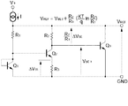
| JP2576433B2 (ja) * | 1994-12-14 | 1997-01-29 | 日本電気株式会社 | 半導体装置用保護回路 |
| US5576579A (en) * | 1995-01-12 | 1996-11-19 | International Business Machines Corporation | Tasin oxygen diffusion barrier in multilayer structures |
| US6153519A (en) * | 1997-03-31 | 2000-11-28 | Motorola, Inc. | Method of forming a barrier layer |
| JPH11195711A (ja) * | 1997-10-27 | 1999-07-21 | Seiko Epson Corp | 半導体装置およびその製造方法 |
| KR100257079B1 (ko) * | 1997-12-05 | 2000-05-15 | 김영환 | 반도체소자 및 이의 제조방법 |
| JP2000268562A (ja) * | 1999-03-15 | 2000-09-29 | Hitachi Ltd | 半導体集積回路装置 |
| TW468271B (en) * | 1999-03-26 | 2001-12-11 | United Microelectronics Corp | Thin film resistor used in a semiconductor chip and its manufacturing method |
| JP2000332203A (ja) * | 1999-05-17 | 2000-11-30 | Hitachi Ltd | 半導体装置およびその製造方法 |
| US6403472B1 (en) * | 1999-06-23 | 2002-06-11 | Harris Corporation | Method of forming resistive contacts on intergrated circuits with mobility spoiling ions including high resistive contacts and low resistivity silicide contacts |
| US7655555B2 (en) * | 1999-08-27 | 2010-02-02 | Texas Instruments Incorporated | In-situ co-deposition of Si in diffusion barrier material depositions with improved wettability, barrier efficiency, and device reliability |
| JP3664655B2 (ja) | 2000-03-13 | 2005-06-29 | 進工業株式会社 | 高比抵抗材料とその製造方法 |
| US20020033750A1 (en) * | 2000-06-13 | 2002-03-21 | Munenori Oizumi | Production method of fine resistor thin film with very low TCR for inkjet printer |
| JP2002141303A (ja) * | 2000-07-27 | 2002-05-17 | Texas Instruments Inc | 向上した濡れ性、障壁効率、デバイス信頼性を有する拡散障壁材料におけるSiの現場同時堆積 |
| JP4149647B2 (ja) * | 2000-09-28 | 2008-09-10 | 株式会社東芝 | 半導体記憶装置及びその製造方法 |
| US6700203B1 (en) * | 2000-10-11 | 2004-03-02 | International Business Machines Corporation | Semiconductor structure having in-situ formed unit resistors |
| JP2002124629A (ja) * | 2000-10-13 | 2002-04-26 | Seiko Instruments Inc | 半導体装置 |
| US6869157B2 (en) * | 2001-03-26 | 2005-03-22 | Canon Kabushiki Kaisha | Method of driving and controlling ink jet print head, ink jet print head, and ink jet printer |
| US6524908B2 (en) * | 2001-06-01 | 2003-02-25 | International Business Machines Corporation | Method for forming refractory metal-silicon-nitrogen capacitors and structures formed |
| US7081271B2 (en) * | 2001-12-07 | 2006-07-25 | Applied Materials, Inc. | Cyclical deposition of refractory metal silicon nitride |
| US6785159B2 (en) * | 2002-08-29 | 2004-08-31 | Micron Technology, Inc. | Combination etch stop and in situ resistor in a magnetoresistive memory and methods for fabricating same |
| US6759729B1 (en) * | 2002-10-16 | 2004-07-06 | Newport Fab, Llc | Temperature insensitive resistor in an IC chip |
| JP2004304068A (ja) * | 2003-03-31 | 2004-10-28 | Denso Corp | 半導体装置及びその製造方法 |
| JP2004342705A (ja) | 2003-05-13 | 2004-12-02 | Cimeo Precision Co Ltd | 窒化タンタル薄膜抵抗体及びその製造方法 |
| KR100524963B1 (ko) * | 2003-05-14 | 2005-10-31 | 삼성전자주식회사 | 금속 배선 및 금속 저항을 포함하는 반도체 소자 및 그제조 방법 |
| US7323751B2 (en) * | 2003-06-03 | 2008-01-29 | Texas Instruments Incorporated | Thin film resistor integration in a dual damascene structure |
| US6861350B1 (en) * | 2003-06-19 | 2005-03-01 | Advanced Micro Devices, Inc. | Method of manufacturing semiconductor device comprising silicon-rich tasin metal gate electrode |
| US6943097B2 (en) * | 2003-08-19 | 2005-09-13 | International Business Machines Corporation | Atomic layer deposition of metallic contacts, gates and diffusion barriers |
| US7317221B2 (en) * | 2003-12-04 | 2008-01-08 | Taiwan Semiconductor Manufacturing Co., Ltd. | High density MIM capacitor structure and fabrication process |
| US7183593B2 (en) * | 2003-12-05 | 2007-02-27 | Taiwan Semiconductor Manufacturing Company, Ltd. | Heterostructure resistor and method of forming the same |
| KR100593444B1 (ko) * | 2004-02-12 | 2006-06-28 | 삼성전자주식회사 | 모오스 바렉터를 갖는 반도체소자 및 그것을 제조하는 방법 |
| US8133364B2 (en) * | 2004-02-17 | 2012-03-13 | Advanced Integration, Inc. | Formation of photoconductive and photovoltaic films |
| US7205634B2 (en) * | 2004-03-10 | 2007-04-17 | Taiwan Semiconductor Manufacturing Co., Ltd. | MIM structure and fabrication process with improved capacitance reliability |
| US8227893B2 (en) * | 2004-06-23 | 2012-07-24 | Nec Corporation | Semiconductor device with capacitor element |
| KR100602087B1 (ko) * | 2004-07-09 | 2006-07-14 | 동부일렉트로닉스 주식회사 | 반도체 소자 및 그 제조방법 |
| KR100695889B1 (ko) * | 2004-10-11 | 2007-03-19 | 삼성전자주식회사 | 반응 방지막을 갖는 캐패시터 및 그 형성 방법 |
| KR100568515B1 (ko) * | 2004-12-06 | 2006-04-07 | 삼성전자주식회사 | 저항 소자를 구비한 반도체소자 및 그 제조방법 |
| KR100639458B1 (ko) * | 2004-12-30 | 2006-10-26 | 동부일렉트로닉스 주식회사 | TaSIN막을 사용한 확산 방지막 형성 방법 및 이를이용한 금속 배선 형성 방법 |
| JP4742758B2 (ja) | 2005-09-06 | 2011-08-10 | 住友金属鉱山株式会社 | 薄膜抵抗体及びその製造方法 |
| US7796426B2 (en) * | 2005-10-17 | 2010-09-14 | Renesas Technology Corp. | Semiconductor device |
| US7602068B2 (en) * | 2006-01-19 | 2009-10-13 | International Machines Corporation | Dual-damascene process to fabricate thick wire structure |
| JP4977400B2 (ja) * | 2006-05-09 | 2012-07-18 | 日本電気株式会社 | 半導体装置及びその製造方法 |
| JP4622946B2 (ja) | 2006-06-29 | 2011-02-02 | 住友金属鉱山株式会社 | 抵抗薄膜材料、抵抗薄膜形成用スパッタリングターゲット、抵抗薄膜、薄膜抵抗器およびその製造方法。 |
| US7932548B2 (en) * | 2006-07-14 | 2011-04-26 | 4D-S Pty Ltd. | Systems and methods for fabricating self-aligned memory cell |
| JP5534170B2 (ja) * | 2007-03-19 | 2014-06-25 | 日本電気株式会社 | 半導体装置及びその製造方法 |
| US8013394B2 (en) * | 2007-03-28 | 2011-09-06 | International Business Machines Corporation | Integrated circuit having resistor between BEOL interconnect and FEOL structure and related method |
| US7972470B2 (en) * | 2007-05-03 | 2011-07-05 | Applied Materials, Inc. | Asymmetric grounding of rectangular susceptor |
| JP5210559B2 (ja) | 2007-07-13 | 2013-06-12 | 株式会社日立製作所 | 半導体装置およびその製造方法 |
| US7719887B2 (en) * | 2007-08-27 | 2010-05-18 | International Business Machines Corporation | CMOS storage devices configurable in high performance mode or radiation tolerant mode |
| JP5334199B2 (ja) * | 2008-01-22 | 2013-11-06 | ルネサスエレクトロニクス株式会社 | 容量素子を有する半導体装置 |
| JP2009283497A (ja) * | 2008-05-19 | 2009-12-03 | Nec Electronics Corp | 半導体装置及び半導体装置の製造方法 |
| US8089135B2 (en) * | 2008-07-30 | 2012-01-03 | International Business Machine Corporation | Back-end-of-line wiring structures with integrated passive elements and design structures for a radiofrequency integrated circuit |
| KR20100111531A (ko) * | 2009-04-07 | 2010-10-15 | 삼성전자주식회사 | 다이오드를 갖는 메모리 장치 및 그 제조 방법 |
| US8243506B2 (en) * | 2010-08-26 | 2012-08-14 | Micron Technology, Inc. | Phase change memory structures and methods |
| US9016133B2 (en) * | 2011-01-05 | 2015-04-28 | Nxp, B.V. | Pressure sensor with pressure-actuated switch |
| US8530320B2 (en) * | 2011-06-08 | 2013-09-10 | International Business Machines Corporation | High-nitrogen content metal resistor and method of forming same |
| US8779407B2 (en) * | 2012-02-07 | 2014-07-15 | Intermolecular, Inc. | Multifunctional electrode |
| US9064902B2 (en) * | 2013-02-27 | 2015-06-23 | Kabushiki Kaisha Toshiba | Semiconductor memory device and method for manufacturing same |
| US8828866B1 (en) * | 2013-06-26 | 2014-09-09 | Applied Materials, Inc. | Methods for depositing a tantalum silicon nitride film |
-
2011
- 2011-11-07 JP JP2011243266A patent/JP5824330B2/ja not_active Expired - Fee Related
-
2012
- 2012-11-06 US US13/670,138 patent/US8829649B2/en active Active
-
2014
- 2014-08-13 US US14/458,976 patent/US20140357047A1/en not_active Abandoned
Also Published As
| Publication number | Publication date |
|---|---|
| US8829649B2 (en) | 2014-09-09 |
| US20130168817A1 (en) | 2013-07-04 |
| US20140357047A1 (en) | 2014-12-04 |
| JP2013098519A (ja) | 2013-05-20 |
Similar Documents
| Publication | Publication Date | Title |
|---|---|---|
| US7012499B2 (en) | Method of fabrication of thin film resistor with 0 TCR | |
| JP5824330B2 (ja) | 半導体装置及び半導体装置の製造方法 | |
| CN202259277U (zh) | 集成电路 | |
| CN101800221B (zh) | 半导体器件 | |
| US11676993B2 (en) | Method and structure for dual sheet resistance trimmable thin film resistors | |
| US6621404B1 (en) | Low temperature coefficient resistor | |
| US7550819B2 (en) | Metal thin-film resistance element on an insulation film | |
| JP4610205B2 (ja) | 半導体装置 | |
| JP2011061005A (ja) | 電子デバイス | |
| TW202225087A (zh) | 半導體結構 | |
| US7956672B2 (en) | Reference voltage generating circuit | |
| JP5025774B2 (ja) | 半導体装置の製造方法 | |
| JP4646891B2 (ja) | 半導体装置及びその製造方法 | |
| CN107785351B (zh) | 零温度系数电阻组件及其制造方法 | |
| JP4610247B2 (ja) | 半導体装置及びその製造方法 | |
| JP5880215B2 (ja) | 抵抗素子の製造方法、抵抗素子および半導体装置 | |
| US20250204256A1 (en) | Thermoelectric conversion element | |
| JP2535721B2 (ja) | 絶縁ゲイト型半導体装置 | |
| JP2005268749A (ja) | 半導体装置 | |
| JP4776234B2 (ja) | 半導体装置の製造方法 | |
| TW202514922A (zh) | 半導體結構及其形成方法 | |
| JP2009239068A (ja) | 半導体装置及びその製造方法 | |
| US20170207209A1 (en) | Integrated circuits with high voltage and high density capacitors and methods of producing the same | |
| JP2009239069A (ja) | 半導体装置及びその製造方法 |
Legal Events
| Date | Code | Title | Description |
|---|---|---|---|
| A521 | Request for written amendment filed |
Free format text: JAPANESE INTERMEDIATE CODE: A523 Effective date: 20140804 |
|
| A621 | Written request for application examination |
Free format text: JAPANESE INTERMEDIATE CODE: A621 Effective date: 20140804 |
|
| A977 | Report on retrieval |
Free format text: JAPANESE INTERMEDIATE CODE: A971007 Effective date: 20150716 |
|
| A131 | Notification of reasons for refusal |
Free format text: JAPANESE INTERMEDIATE CODE: A131 Effective date: 20150728 |
|
| A521 | Request for written amendment filed |
Free format text: JAPANESE INTERMEDIATE CODE: A523 Effective date: 20150909 |
|
| TRDD | Decision of grant or rejection written | ||
| A01 | Written decision to grant a patent or to grant a registration (utility model) |
Free format text: JAPANESE INTERMEDIATE CODE: A01 Effective date: 20150929 |
|
| A61 | First payment of annual fees (during grant procedure) |
Free format text: JAPANESE INTERMEDIATE CODE: A61 Effective date: 20151009 |
|
| R150 | Certificate of patent or registration of utility model |
Ref document number: 5824330 Country of ref document: JP Free format text: JAPANESE INTERMEDIATE CODE: R150 |
|
| LAPS | Cancellation because of no payment of annual fees |