JP5783706B2 - プリント回路板 - Google Patents
プリント回路板 Download PDFInfo
- Publication number
- JP5783706B2 JP5783706B2 JP2010248188A JP2010248188A JP5783706B2 JP 5783706 B2 JP5783706 B2 JP 5783706B2 JP 2010248188 A JP2010248188 A JP 2010248188A JP 2010248188 A JP2010248188 A JP 2010248188A JP 5783706 B2 JP5783706 B2 JP 5783706B2
- Authority
- JP
- Japan
- Prior art keywords
- hole
- corner
- printed wiring
- wiring board
- electronic component
- Prior art date
- Legal status (The legal status is an assumption and is not a legal conclusion. Google has not performed a legal analysis and makes no representation as to the accuracy of the status listed.)
- Expired - Fee Related
Links
Images


Classifications
-
- H—ELECTRICITY
- H10—SEMICONDUCTOR DEVICES; ELECTRIC SOLID-STATE DEVICES NOT OTHERWISE PROVIDED FOR
- H10W—GENERIC PACKAGES, INTERCONNECTIONS, CONNECTORS OR OTHER CONSTRUCTIONAL DETAILS OF DEVICES COVERED BY CLASS H10
- H10W90/00—Package configurations
- H10W90/701—Package configurations characterised by the relative positions of pads or connectors relative to package parts
- H10W90/721—Package configurations characterised by the relative positions of pads or connectors relative to package parts of bump connectors
- H10W90/724—Package configurations characterised by the relative positions of pads or connectors relative to package parts of bump connectors between a chip and a stacked insulating package substrate, interposer or RDL
Landscapes
- Structures For Mounting Electric Components On Printed Circuit Boards (AREA)
- Structure Of Printed Boards (AREA)
- Wire Bonding (AREA)
Description
また、本発明のプリント回路板は、マトリクス形状に配置された端子を備えた電子部品をプリント配線板に搭載したプリント回路板において、前記電子部品のマトリクス形状の角部のうち少なくとも一つの角部には端子がなく、前記プリント配線板には、前記少なくとも一つの角部以外の位置に設けられた端子と接合した複数のランドと、前記少なくとも一つの角部に対向する位置に設けられた貫通孔又は非貫通孔と、が設けられており、前記電子部品のマトリクス形状の少なくとも一つの角部の位置において、前記電子部品と前記プリント配線板が接合されておらず、前記プリント配線板の撓みによって発生する応力を前記貫通孔又は前記非貫通孔のまわりに集中させ、前記少なくとも一つの角部の周囲に位置する端子に伝わる応力を低減することを特徴とする。
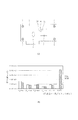
2、12 電子部品
2a、12a 端子
2b 角部端子
3、13 ランド
4、14a〜14d 貫通孔
Claims (6)
- マトリクス形状に配置された端子を備えた電子部品をプリント配線板に搭載したプリント回路板において、
前記プリント配線板には、
前記電子部品のマトリクス形状の少なくとも一つの角部の電気信号を伝えない端子に対向するように設けられた貫通孔又は非貫通孔と、
前記少なくとも一つの角部に位置する端子以外の端子と接合した複数のランドと、
が設けられており、
前記電子部品のマトリクス形状の少なくとも一つの角部の位置において、前記電子部品と前記プリント配線板が接合されておらず、
前記プリント配線板の撓みによって発生する応力を前記貫通孔又は前記非貫通孔のまわりに集中させ、前記少なくとも一つの角部の周囲に位置する端子に伝わる応力を低減することを特徴とするプリント回路板。 - 前記マトリクス形状に配置された端子の直径は等しいことを特徴とする請求項1に記載のプリント回路板。
- 前記貫通孔又は非貫通孔の開口部の直径は、0.4mm以上1mm以下であることを特徴とする請求項1又は2に記載のプリント回路板。
- マトリクス形状に配置された端子を備えた電子部品をプリント配線板に搭載したプリント回路板において、
前記電子部品のマトリクス形状の角部のうち少なくとも一つの角部には端子がなく、
前記プリント配線板には、
前記少なくとも一つの角部以外の位置に設けられた端子と接合した複数のランドと、
前記少なくとも一つの角部に対向する位置に設けられた貫通孔又は非貫通孔と、
が設けられており、
前記電子部品のマトリクス形状の少なくとも一つの角部の位置において、前記電子部品と前記プリント配線板が接合されておらず、
前記プリント配線板の撓みによって発生する応力を前記貫通孔又は前記非貫通孔のまわりに集中させ、前記少なくとも一つの角部の周囲に位置する端子に伝わる応力を低減することを特徴とするプリント回路板。 - 前記貫通孔又は非貫通孔の開口部の直径は、0.4mm以上1mm以下であることを特徴とする請求項4に記載のプリント回路板。
- 前記貫通孔又は前記非貫通孔には、前記プリント配線板の層間の配線を電気的に接続する金属メッキが施されていることを特徴とする請求項4又は5に記載のプリント回路板。
Priority Applications (1)
| Application Number | Priority Date | Filing Date | Title |
|---|---|---|---|
| JP2010248188A JP5783706B2 (ja) | 2010-11-05 | 2010-11-05 | プリント回路板 |
Applications Claiming Priority (1)
| Application Number | Priority Date | Filing Date | Title |
|---|---|---|---|
| JP2010248188A JP5783706B2 (ja) | 2010-11-05 | 2010-11-05 | プリント回路板 |
Publications (3)
| Publication Number | Publication Date |
|---|---|
| JP2012099751A JP2012099751A (ja) | 2012-05-24 |
| JP2012099751A5 JP2012099751A5 (ja) | 2013-12-19 |
| JP5783706B2 true JP5783706B2 (ja) | 2015-09-24 |
Family
ID=46391299
Family Applications (1)
| Application Number | Title | Priority Date | Filing Date |
|---|---|---|---|
| JP2010248188A Expired - Fee Related JP5783706B2 (ja) | 2010-11-05 | 2010-11-05 | プリント回路板 |
Country Status (1)
| Country | Link |
|---|---|
| JP (1) | JP5783706B2 (ja) |
Families Citing this family (2)
| Publication number | Priority date | Publication date | Assignee | Title |
|---|---|---|---|---|
| KR102837100B1 (ko) * | 2020-01-14 | 2025-07-22 | 주식회사 엘지에너지솔루션 | Bmu 부품 손상 방지 구조를 포함하는 배터리 팩 |
| CN115996513B (zh) * | 2021-10-19 | 2025-06-20 | 礼鼎半导体科技秦皇岛有限公司 | 封装芯片、封装结构、电路板及其制造方法 |
Family Cites Families (8)
| Publication number | Priority date | Publication date | Assignee | Title |
|---|---|---|---|---|
| JPH11111771A (ja) * | 1997-10-07 | 1999-04-23 | Matsushita Electric Ind Co Ltd | 配線基板の接続方法、キャリア基板および配線基板 |
| JPH11111772A (ja) * | 1997-10-07 | 1999-04-23 | Matsushita Electric Ind Co Ltd | キャリア基板の実装位置決め方法、キャリア基板および配線基板 |
| JP2001119107A (ja) * | 1999-10-19 | 2001-04-27 | Nec Saitama Ltd | プリント配線板 |
| JP2001144116A (ja) * | 1999-11-11 | 2001-05-25 | Hitachi Kokusai Electric Inc | 電子部品の実装方法及び構造、並びに回路基板 |
| JP4273598B2 (ja) * | 1999-11-22 | 2009-06-03 | パナソニック株式会社 | Bga型パッケージを搭載する回路基板 |
| JP5017991B2 (ja) * | 2006-09-28 | 2012-09-05 | 富士通株式会社 | プリント配線板、電子装置 |
| JP2009130048A (ja) * | 2007-11-21 | 2009-06-11 | Elpida Memory Inc | 半導体装置及び電子装置 |
| JP2010010428A (ja) * | 2008-06-27 | 2010-01-14 | Fujitsu Ltd | プリント基板及び電子機器 |
-
2010
- 2010-11-05 JP JP2010248188A patent/JP5783706B2/ja not_active Expired - Fee Related
Also Published As
| Publication number | Publication date |
|---|---|
| JP2012099751A (ja) | 2012-05-24 |
Similar Documents
| Publication | Publication Date | Title |
|---|---|---|
| JP6325605B2 (ja) | 電子部品内蔵基板 | |
| KR101062538B1 (ko) | 다층 회로기판을 연결하는 기술 | |
| JP5503567B2 (ja) | 半導体装置および半導体装置実装体 | |
| CN102281715B (zh) | 板加强结构、板组件、以及电子装置 | |
| JP2013219170A (ja) | 基板装置 | |
| US20100252936A1 (en) | Semiconductor module and portable devices | |
| JP5146019B2 (ja) | 高周波モジュールとこれを用いた電子機器 | |
| JP5783706B2 (ja) | プリント回路板 | |
| US20100327452A1 (en) | Mounting structure and method of manufacturing the same | |
| US9510462B2 (en) | Method for fabricating circuit board structure | |
| JP2002344092A (ja) | プリント基板 | |
| JP2005150490A (ja) | Icとプリント配線基板間のシート部品 | |
| JP2015026835A (ja) | 印刷回路基板 | |
| JP2008141036A (ja) | プリント基板およびその製造方法 | |
| JP2010118592A (ja) | 半導体装置 | |
| JP6089557B2 (ja) | 電子部品モジュール | |
| KR20100123415A (ko) | 인쇄회로기판 | |
| JP2016207612A (ja) | コネクタ、及び電子機器 | |
| JP2008047605A (ja) | プリント基板 | |
| JPH11346036A (ja) | 電気基板および電気実装装着方法 | |
| JP5017991B2 (ja) | プリント配線板、電子装置 | |
| JPWO2006082633A1 (ja) | パッケージ実装モジュール | |
| JP2013110332A (ja) | 表面実装電子デバイス | |
| JP2010010413A (ja) | 多層プリント配線基板、及び多層プリント配線基板装置 | |
| JP2008034672A (ja) | チップ部品の実装方法および電子モジュール |
Legal Events
| Date | Code | Title | Description |
|---|---|---|---|
| RD04 | Notification of resignation of power of attorney |
Free format text: JAPANESE INTERMEDIATE CODE: A7424 Effective date: 20130228 |
|
| A521 | Request for written amendment filed |
Free format text: JAPANESE INTERMEDIATE CODE: A523 Effective date: 20131105 |
|
| A621 | Written request for application examination |
Free format text: JAPANESE INTERMEDIATE CODE: A621 Effective date: 20131105 |
|
| A977 | Report on retrieval |
Free format text: JAPANESE INTERMEDIATE CODE: A971007 Effective date: 20140523 |
|
| A131 | Notification of reasons for refusal |
Free format text: JAPANESE INTERMEDIATE CODE: A131 Effective date: 20140527 |
|
| A521 | Request for written amendment filed |
Free format text: JAPANESE INTERMEDIATE CODE: A523 Effective date: 20140728 |
|
| A131 | Notification of reasons for refusal |
Free format text: JAPANESE INTERMEDIATE CODE: A131 Effective date: 20141111 |
|
| A521 | Request for written amendment filed |
Free format text: JAPANESE INTERMEDIATE CODE: A523 Effective date: 20150113 |
|
| TRDD | Decision of grant or rejection written | ||
| A01 | Written decision to grant a patent or to grant a registration (utility model) |
Free format text: JAPANESE INTERMEDIATE CODE: A01 Effective date: 20150623 |
|
| A61 | First payment of annual fees (during grant procedure) |
Free format text: JAPANESE INTERMEDIATE CODE: A61 Effective date: 20150721 |
|
| R151 | Written notification of patent or utility model registration |
Ref document number: 5783706 Country of ref document: JP Free format text: JAPANESE INTERMEDIATE CODE: R151 |
|
| LAPS | Cancellation because of no payment of annual fees |