JP5783706B2 - Printed circuit board - Google Patents
Printed circuit board Download PDFInfo
- Publication number
- JP5783706B2 JP5783706B2 JP2010248188A JP2010248188A JP5783706B2 JP 5783706 B2 JP5783706 B2 JP 5783706B2 JP 2010248188 A JP2010248188 A JP 2010248188A JP 2010248188 A JP2010248188 A JP 2010248188A JP 5783706 B2 JP5783706 B2 JP 5783706B2
- Authority
- JP
- Japan
- Prior art keywords
- hole
- corner
- printed wiring
- wiring board
- electronic component
- Prior art date
- Legal status (The legal status is an assumption and is not a legal conclusion. Google has not performed a legal analysis and makes no representation as to the accuracy of the status listed.)
- Expired - Fee Related
Links
Images


Classifications
-
- H—ELECTRICITY
- H01—ELECTRIC ELEMENTS
- H01L—SEMICONDUCTOR DEVICES NOT COVERED BY CLASS H10
- H01L2224/00—Indexing scheme for arrangements for connecting or disconnecting semiconductor or solid-state bodies and methods related thereto as covered by H01L24/00
- H01L2224/01—Means for bonding being attached to, or being formed on, the surface to be connected, e.g. chip-to-package, die-attach, "first-level" interconnects; Manufacturing methods related thereto
- H01L2224/10—Bump connectors; Manufacturing methods related thereto
- H01L2224/15—Structure, shape, material or disposition of the bump connectors after the connecting process
- H01L2224/16—Structure, shape, material or disposition of the bump connectors after the connecting process of an individual bump connector
- H01L2224/161—Disposition
- H01L2224/16151—Disposition the bump connector connecting between a semiconductor or solid-state body and an item not being a semiconductor or solid-state body, e.g. chip-to-substrate, chip-to-passive
- H01L2224/16221—Disposition the bump connector connecting between a semiconductor or solid-state body and an item not being a semiconductor or solid-state body, e.g. chip-to-substrate, chip-to-passive the body and the item being stacked
- H01L2224/16225—Disposition the bump connector connecting between a semiconductor or solid-state body and an item not being a semiconductor or solid-state body, e.g. chip-to-substrate, chip-to-passive the body and the item being stacked the item being non-metallic, e.g. insulating substrate with or without metallisation
Description
本発明は、マトリクス形状に配置された端子接合部を有するプリント回路板に関するものである。 The present invention relates to a printed circuit board having terminal joint portions arranged in a matrix shape.
携帯型の小型電子機器において、昨今では、製品の小型化が進んでおり、内蔵されるプリント配線板やそれに搭載される電子部品も小型化が余儀なくされている。従来、プリント配線板に搭載される電子部品は、外周に設けられたリード端子電極をプリント配線板に接合する形態が用いられていた。しかし、電子部品は小型化のために、電極を電子部品の裏面にマトリクス形状に配置して小型化した構造へ変化してきている。そのような構造のものとして、ボール電極をプリント配線板に接合するBGA(Ball Grid Array)やCSP(Chip Size Package)と呼ばれる電子部品が多用されている。 Recently, miniaturization of products has been progressing in portable small electronic devices, and the built-in printed wiring boards and electronic components mounted on the printed wiring boards have been forced to be miniaturized. Conventionally, an electronic component mounted on a printed wiring board has a form in which lead terminal electrodes provided on the outer periphery are joined to the printed wiring board. However, in order to reduce the size of electronic parts, the structure has been reduced to a structure in which electrodes are arranged in a matrix on the back surface of the electronic part. As such a structure, electronic parts called BGA (Ball Grid Array) and CSP (Chip Size Package) for joining ball electrodes to a printed wiring board are often used.
リード電極はプリント配線板の撓みが発生した場合に、リードの追従により応力を軽減する効果があったが、ボール電極には撓みを吸収する柔軟性がないため、基板との接合部に応力が集中し、接合部が破断しやすくなっている。 The lead electrode had the effect of reducing the stress by following the lead when the printed wiring board was bent, but the ball electrode does not have the flexibility to absorb the bending, so there is no stress at the joint with the board. It concentrates and the joint is easy to break.
特に、マトリクス形状に端子電極を配置した電子部品の場合は、プリント配線板の撓みによって端子の接合部に発生する応力は、端子の位置によって異なる。撓みの影響を直接受ける外周部が特に応力が大きく、その中でも角部に位置する端子の接合部は隣接する端子が少ないため、最も大きな応力が発生し、接合部が破断しやすい。 In particular, in the case of an electronic component in which terminal electrodes are arranged in a matrix shape, the stress generated at the joint portion of the terminal due to the bending of the printed wiring board varies depending on the position of the terminal. The outer peripheral portion directly affected by the bending is particularly stressed, and among them, the joint portion of the terminal located at the corner portion has few adjacent terminals, so that the largest stress is generated and the joint portion is easily broken.
また、製品の小型化を図る目的でプリント配線板の薄型化も一段と進んでいる。そのため、外部応力によりプリント配線板が撓み易く、電子部品の端子接合部に大きな応力がかかり、接合部が破断しやすくなっている。 In addition, printed wiring boards are being made thinner for the purpose of product miniaturization. Therefore, the printed wiring board is easily bent by external stress, and a large stress is applied to the terminal joint portion of the electronic component, and the joint portion is easily broken.
このような状況から、外部応力による端子接合部の破断が直接電気的な性能に影響を及ぼさないよう、電子部品の角部端子の電気信号を用いないで、補強用の端子として用いることが一般的に行なわれている。また、図4に示すように、電子部品102の角部への応力集中を回避するため、電子部品102の角部端子の接合部に沿うように、プリント配線板101にスリット孔104を設ける提案がされている(特許文献1参照)。
From such a situation, it is common to use it as a reinforcing terminal without using the electrical signal of the corner terminal of the electronic component so that the breakage of the terminal joint due to external stress does not directly affect the electrical performance Has been done. Further, as shown in FIG. 4, in order to avoid stress concentration on the corners of the
従来技術のように、応力が集中しやすい角部端子を補強用の端子とする場合、角部端子の接合部が破断しても電気的な機能には影響を及ぼすことはない。しかし、破断後は補強部の接合がなくなることにより、基板の撓みによって、破断した端子の周囲の端子接合部に強い応力が発生する。破断した状態が検出されず製品に搭載されることになると、製品に加わる衝撃で、破断した端子周辺の接合部のひびや破断を招く危険性がある。接合部にひびがはいると製品が誤動作する懸念があり、接合部が破断に至ると最悪の場合、製品が動作しない。 When the corner terminal where stress is likely to concentrate is used as a reinforcing terminal as in the prior art, the electrical function is not affected even if the joint portion of the corner terminal is broken. However, after the breakage, the joining of the reinforcing portion disappears, and a strong stress is generated in the terminal joint portion around the broken terminal due to the bending of the substrate. When a broken state is not detected and the product is mounted on a product, there is a risk that an impact applied to the product may cause cracks or breakage of the joint around the broken terminal. If the joint is cracked, the product may malfunction, and if the joint is broken, the product does not operate in the worst case.
また、電子部品の角部に沿った形状でスリット孔を設けることで、角部及び角部周囲に発生する強い応力を緩和する構成では、電子部品から引き出される電気配線領域を大きく制限するという問題があった。 In addition, by providing slit holes in a shape along the corner of the electronic component to relieve the strong stress generated around the corner and the corner, the electric wiring area drawn from the electronic component is greatly limited. was there.
本発明は、電子部品の角部におけるプリント配線板との接合部の応力集中を効果的に低減できるプリント回路板を提供することを目的とするものである。 It is an object of the present invention to provide a printed circuit board that can effectively reduce stress concentration at a joint portion with a printed wiring board at a corner of an electronic component.
本発明のプリント回路板は、マトリクス形状に配置された端子を備えた電子部品をプリント配線板に搭載したプリント回路板において、前記プリント配線板には、前記電子部品のマトリクス形状の少なくとも一つの角部の電気信号を伝えない端子に対向するように設けられた貫通孔又は非貫通孔と、前記少なくとも一つの角部に位置する端子以外の端子と接合した複数のランドと、が設けられており、前記電子部品のマトリクス形状の少なくとも一つの角部の位置において、前記電子部品と前記プリント配線板が接合されておらず、前記プリント配線板の撓みによって発生する応力を前記貫通孔又は前記非貫通孔のまわりに集中させ、前記少なくとも一つの角部の周囲に位置する端子に伝わる応力を低減することを特徴とする。
また、本発明のプリント回路板は、マトリクス形状に配置された端子を備えた電子部品をプリント配線板に搭載したプリント回路板において、前記電子部品のマトリクス形状の角部のうち少なくとも一つの角部には端子がなく、前記プリント配線板には、前記少なくとも一つの角部以外の位置に設けられた端子と接合した複数のランドと、前記少なくとも一つの角部に対向する位置に設けられた貫通孔又は非貫通孔と、が設けられており、前記電子部品のマトリクス形状の少なくとも一つの角部の位置において、前記電子部品と前記プリント配線板が接合されておらず、前記プリント配線板の撓みによって発生する応力を前記貫通孔又は前記非貫通孔のまわりに集中させ、前記少なくとも一つの角部の周囲に位置する端子に伝わる応力を低減することを特徴とする。
The printed circuit board of the present invention is a printed circuit board in which an electronic component having terminals arranged in a matrix shape is mounted on the printed wiring board, and the printed wiring board includes at least one corner of the matrix shape of the electronic component. a through hole or non-through-hole is provided so as to face the terminal does not transmit an electrical signal parts, and the at least one corner plurality of joined with terminals other than terminals located in the part land, is provided with The electronic component and the printed wiring board are not joined at the position of at least one corner of the matrix shape of the electronic component, and stress generated by bending of the printed wiring board is caused by the through hole or the non-through hole. The stress transmitted to the terminals located around the at least one corner portion is reduced by being concentrated around the hole .
The printed circuit board according to the present invention is a printed circuit board in which an electronic component having terminals arranged in a matrix shape is mounted on a printed wiring board, and at least one corner portion of the matrix shape corner portion of the electronic component. The printed wiring board has a plurality of lands joined to terminals provided at positions other than the at least one corner, and a through hole provided at a position facing the at least one corner. A hole or a non-through hole is provided , and the electronic component and the printed wiring board are not joined at the position of at least one corner of the matrix shape of the electronic component, and the printed wiring board is bent. to concentrate stress generated around the through-hole or the blind holes by reducing the stress transmitted to the terminals located around at least one corner And wherein the Rukoto.
強い応力の発生する電子部品の角部において、端子の接合部を設けないことで、接合部の破断の危険性を回避できる。さらに、プリント配線板側の応力が集中する領域に貫通孔もしくは非貫通孔を設けることによって、電子部品の角部周辺の端子の接合部にかかる応力を緩和することができる。 The risk of breakage of the joint can be avoided by not providing the terminal joint at the corner of the electronic component where strong stress occurs. Furthermore, by providing a through hole or a non-through hole in a region where stress on the printed wiring board side is concentrated, it is possible to relieve the stress applied to the joint portion of the terminal around the corner of the electronic component.
電子部品の角部に位置する端子接合部の破断の原因となる応力をプリント配線板側で吸収できるため、角部周辺の端子の接合部での破断の発生を防止することが可能となる。 Since the stress that causes the breakage of the terminal joint located at the corner of the electronic component can be absorbed on the printed wiring board side, it is possible to prevent the breakage at the joint of the terminal around the corner.
また、応力が集中する位置に設ける貫通孔もしくは非貫通孔は、サイズが小さくても応力緩和に有効であるため、電子部品から引き出される信号配線への影響を最小限に留めることが可能となる。 In addition, since the through hole or non-through hole provided at a position where stress is concentrated is effective for stress relaxation even if the size is small, it is possible to minimize the influence on the signal wiring drawn from the electronic component. .
図1は、実施例1によるプリント回路板を示す。図1に示すように、プリント配線板1には、角部を有するマトリクス形状に配置された端子を備え、そのうちの角部端子2bは電気信号を伝えない電子部品2が実装(搭載)される。プリント配線板1上には、電子部品2を接続するために、角部端子2bを除く残りの端子2aに接合するようにマトリクス形状に配置されたランド3が形成されている。プリント配線板1には、電子部品2の角部端子2bに対応する接続ランドは設けず、マトリクス形状の角部に貫通孔(又は非貫通孔)4が設けられている。
FIG. 1 shows a printed circuit board according to the first embodiment. As shown in FIG. 1, the printed wiring board 1 includes terminals arranged in a matrix shape having corners, and the
プリント配線板1のサイズは、例えばデジタルカメラの内蔵基板として用いられるもので、80×40mm、厚さ0.8mmである。プリント配線板1に実装される電子部品2のサイズは例えば12×12mmであり、ボール電極(端子)の直径は0.5mmである。また、電子部品2の角部に対向する貫通孔4は、レーザーや機械ドリル等を用いた穴開け加工により形成する。例えば0.4mmの貫通孔又は非貫通孔をあけると、そのまわりに応力を集中でき、電子部品2の角部周囲に位置する端子2c、2dの接合部に伝わる応力を低減できる。
The size of the printed wiring board 1 is, for example, used as a built-in substrate of a digital camera, and is 80 × 40 mm and a thickness of 0.8 mm. The size of the
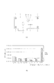
図2(a)に示す応力解析のシミュレーションモデルについて、応力解析の結果を(b)に示す。プリント配線板1は、4箇所のビス締結穴7によって、筐体に固定される。そのため、シミュレーション上はビス締結穴を拘束(変動のない点)として扱う。この状態において、加圧領域8に外圧を加えるとプリント配線板1が撓み、電子部品2の端子接合部に応力が加わる。
FIG. 2B shows the result of the stress analysis for the simulation model of the stress analysis shown in FIG. The printed wiring board 1 is fixed to the housing by four
図2(b)は、貫通孔4の孔径変化に対する電子部品角部周囲に位置する端子2c、2dにかかる応力変化を示している。また、比較対照として、電子部品2の角部端子2bを接合し、貫通孔を設けていないプリント配線板の応力解析結果を併記している。また、従来例との比較として、電子部品2の角部端子2bを接合し、端子2b、2c、2dを覆うようにスリットを設けたプリント配線板の応力解析結果を併記している。図2(b)の応力解析結果より、0.4〜1mm程度の孔径においても、接合部として用いられるはんだの引張強度である50N/mm2程の値と比較して、電子部品2の角部周囲の端子2c、2dにかかる応力は小さくなる。プリント配線板の配線領域を阻害することなく、スリットを設けたプリント配線板と同等、またはそれ以上の応力緩和効果が得られる。
FIG. 2B shows a change in stress applied to the
これにより、例えばコネクタの抜き差しのような組立て時の外圧がプリント配線板1に加えられた場合、電子部品2の角部端子2bを基板と接合しないことで、角部端子2bの接合部に応力を集中させない。そして、角部の接合部から角部周囲に位置する端子2c、2dの接合部に応力が伝わることを軽減する。
Thereby, when external pressure at the time of assembly such as insertion / removal of a connector is applied to the printed wiring board 1, stress is applied to the joint portion of the
さらに、その応力が集中する領域に貫通孔4を設けることにより、プリント配線板1を伝わり電子部品2の角部周囲の端子2c、2dにかかる応力を貫通孔4の周りに寄せて低減可能である。かくして、電子部品2の接合部のひびや破断を回避することができる。
Furthermore, by providing the through
図3は、実施例2によるプリント回路板を示す。図3(a)に示すプリント配線板11には、図3(b)に示すようなマトリクス形状に配置された端子12aを有し、マトリクス形状の角部12eの端子を省略した電子部品12が実装される。プリント配線板11上には、電子部品12を接続するためにマトリクス形状に配置されたランド13が形成されている。
FIG. 3 shows a printed circuit board according to the second embodiment. The printed
マトリクス形状に配置されたランド13のうち、最外周ランド列13a、13bの中心を結んだ2本の直線の交点を含む位置に貫通孔14aが形成されている。また、最外周ランド列13b、13cの中心を結んだ2本の直線の交点を含む位置に貫通孔14bが形成されている。同様に、最外周ランド列13c、13dの中心を結んだ2本の直線の交点を含む位置に貫通孔14cが、最外周ランド列13d、13aの中心を結んだ2本の直線の交点を含む位置に貫通孔14dが形成されている。
A through
プリント配線板11に形成される貫通孔14a〜14dは、プリント配線板11の層間の配線を電気的に接続する金属メッキされた貫通孔又は非貫通孔(スルーホール)であってもよい。貫通孔を金属メッキされたスルーホールとすることで、電子部品12の角部周辺における電気配線の設計自由度を向上することが可能となる。プリント配線板11に加わる外圧の位置が把握できる場合には、外圧の位置によって、貫通孔14a〜14dを適宜選択して設けてもよい。
The through holes 14 a to 14 d formed in the printed
これにより、プリント配線板11は、上下方向から様々な位置に外圧が加えられた場合であっても、電子部品12の角部が接合されていないため、角部に応力を集中させることなく、角部周囲に位置する接合部に応力が伝わることを軽減する。そして、貫通孔14a〜14dを設けることで、プリント配線板11の撓みによって電子部品12のはんだ接合部にかかる応力を貫通孔周りによせることができる。このように、プリント配線板11の様々な位置に加わる外圧から電子部品12の角部周囲にかかる応力を効果的に低減し、電子部品12の接合部のひびや破断を回避することができる。
Thereby, even if the printed
なお実施例1、2においては、プリント配線板に実装される電子部品として、BGA、CSPを用いるような場合について述べた。しかしながら、本発明はこれに限らず、LGA(Land Grid Array)、PGA(Pin Grid Array)などの電子部品を用いた場合も同様な効果が得られる。 In the first and second embodiments, the case where BGA or CSP is used as the electronic component mounted on the printed wiring board has been described. However, the present invention is not limited to this, and the same effect can be obtained when electronic parts such as LGA (Land Grid Array) and PGA (Pin Grid Array) are used.
また、プリント配線板として、筐体に組み込まれるプリント配線板について述べたが、本発明はこれに限らず、電子部品のチップとメインのプリント配線板とを中継するインターポーザ基板を用いた場合も同様の効果が得られる。 Moreover, although the printed wiring board incorporated in a housing | casing was described as a printed wiring board, this invention is not limited to this, It is the same also when using the interposer board which relays the chip | tip of an electronic component, and the main printed wiring board. The effect is obtained.
1、11 プリント配線板
2、12 電子部品
2a、12a 端子
2b 角部端子
3、13 ランド
4、14a〜14d 貫通孔
1, 11 Printed
Claims (6)
前記プリント配線板には、
前記電子部品のマトリクス形状の少なくとも一つの角部の電気信号を伝えない端子に対向するように設けられた貫通孔又は非貫通孔と、
前記少なくとも一つの角部に位置する端子以外の端子と接合した複数のランドと、
が設けられており、
前記電子部品のマトリクス形状の少なくとも一つの角部の位置において、前記電子部品と前記プリント配線板が接合されておらず、
前記プリント配線板の撓みによって発生する応力を前記貫通孔又は前記非貫通孔のまわりに集中させ、前記少なくとも一つの角部の周囲に位置する端子に伝わる応力を低減することを特徴とするプリント回路板。 In a printed circuit board in which electronic components having terminals arranged in a matrix shape are mounted on a printed wiring board,
In the printed wiring board,
A through-hole or a non-through-hole provided so as to face a terminal that does not transmit an electrical signal of at least one corner of the matrix shape of the electronic component ;
A plurality of lands bonded to terminals other than the terminals located at the at least one corner;
Is provided ,
In the position of at least one corner of the matrix shape of the electronic component, the electronic component and the printed wiring board are not joined,
A printed circuit characterized in that stress generated by bending of the printed wiring board is concentrated around the through-hole or the non-through-hole to reduce stress transmitted to terminals located around the at least one corner. Board.
前記電子部品のマトリクス形状の角部のうち少なくとも一つの角部には端子がなく、
前記プリント配線板には、
前記少なくとも一つの角部以外の位置に設けられた端子と接合した複数のランドと、
前記少なくとも一つの角部に対向する位置に設けられた貫通孔又は非貫通孔と、
が設けられており、
前記電子部品のマトリクス形状の少なくとも一つの角部の位置において、前記電子部品と前記プリント配線板が接合されておらず、
前記プリント配線板の撓みによって発生する応力を前記貫通孔又は前記非貫通孔のまわりに集中させ、前記少なくとも一つの角部の周囲に位置する端子に伝わる応力を低減することを特徴とするプリント回路板。 In a printed circuit board in which electronic components having terminals arranged in a matrix shape are mounted on a printed wiring board,
There is no terminal in at least one corner of the matrix-shaped corner of the electronic component,
In the printed wiring board,
A plurality of lands joined to terminals provided at positions other than the at least one corner;
A through hole or a non-through hole provided at a position facing the at least one corner,
Is provided ,
In the position of at least one corner of the matrix shape of the electronic component, the electronic component and the printed wiring board are not joined,
A printed circuit characterized in that stress generated by bending of the printed wiring board is concentrated around the through-hole or the non-through-hole to reduce stress transmitted to terminals located around the at least one corner. Board.
Priority Applications (1)
| Application Number | Priority Date | Filing Date | Title |
|---|---|---|---|
| JP2010248188A JP5783706B2 (en) | 2010-11-05 | 2010-11-05 | Printed circuit board |
Applications Claiming Priority (1)
| Application Number | Priority Date | Filing Date | Title |
|---|---|---|---|
| JP2010248188A JP5783706B2 (en) | 2010-11-05 | 2010-11-05 | Printed circuit board |
Publications (3)
| Publication Number | Publication Date |
|---|---|
| JP2012099751A JP2012099751A (en) | 2012-05-24 |
| JP2012099751A5 JP2012099751A5 (en) | 2013-12-19 |
| JP5783706B2 true JP5783706B2 (en) | 2015-09-24 |
Family
ID=46391299
Family Applications (1)
| Application Number | Title | Priority Date | Filing Date |
|---|---|---|---|
| JP2010248188A Expired - Fee Related JP5783706B2 (en) | 2010-11-05 | 2010-11-05 | Printed circuit board |
Country Status (1)
| Country | Link |
|---|---|
| JP (1) | JP5783706B2 (en) |
Families Citing this family (1)
| Publication number | Priority date | Publication date | Assignee | Title |
|---|---|---|---|---|
| KR20210091556A (en) * | 2020-01-14 | 2021-07-22 | 주식회사 엘지화학 | Battery packs with Battery Management Unit component damage prevention structure |
Family Cites Families (8)
| Publication number | Priority date | Publication date | Assignee | Title |
|---|---|---|---|---|
| JPH11111772A (en) * | 1997-10-07 | 1999-04-23 | Matsushita Electric Ind Co Ltd | Method for setting mounting position of carrier board, the carrier board, and wiring board |
| JPH11111771A (en) * | 1997-10-07 | 1999-04-23 | Matsushita Electric Ind Co Ltd | Method for connecting wiring board, carrier board and wiring board |
| JP2001119107A (en) * | 1999-10-19 | 2001-04-27 | Nec Saitama Ltd | Printed wiring board |
| JP2001144116A (en) * | 1999-11-11 | 2001-05-25 | Hitachi Kokusai Electric Inc | Mounting method for and structure of electronic component, and circuit board |
| JP4273598B2 (en) * | 1999-11-22 | 2009-06-03 | パナソニック株式会社 | Circuit board with BGA package |
| JP5017991B2 (en) * | 2006-09-28 | 2012-09-05 | 富士通株式会社 | Printed wiring boards, electronic devices |
| JP2009130048A (en) * | 2007-11-21 | 2009-06-11 | Elpida Memory Inc | Semiconductor device, and electronic device |
| JP2010010428A (en) * | 2008-06-27 | 2010-01-14 | Fujitsu Ltd | Printed substrate, and electronic device |
-
2010
- 2010-11-05 JP JP2010248188A patent/JP5783706B2/en not_active Expired - Fee Related
Also Published As
| Publication number | Publication date |
|---|---|
| JP2012099751A (en) | 2012-05-24 |
Similar Documents
| Publication | Publication Date | Title |
|---|---|---|
| JP6325605B2 (en) | Electronic component built-in substrate | |
| KR101062538B1 (en) | Technology for connecting multilayer circuit boards | |
| JP5503567B2 (en) | Semiconductor device and semiconductor device mounting body | |
| JP5445340B2 (en) | Substrate reinforcement structure, substrate assembly, and electronic device | |
| JP2006210852A (en) | Circuit board with surface-mounting circuit component, and its manufacture | |
| US20100252936A1 (en) | Semiconductor module and portable devices | |
| US20100327452A1 (en) | Mounting structure and method of manufacturing the same | |
| US20070238324A1 (en) | Electrical connector | |
| JP5783706B2 (en) | Printed circuit board | |
| JP5146019B2 (en) | High frequency module and electronic device using the same | |
| JP2002344092A (en) | Printed board | |
| US9510462B2 (en) | Method for fabricating circuit board structure | |
| JP2005150490A (en) | Sheet component between ic and printed wiring board | |
| JP2010118592A (en) | Semiconductor device | |
| JP2008141036A (en) | Printed substrate and method of manufacturing the same | |
| JP6089557B2 (en) | Electronic component module | |
| JP5017991B2 (en) | Printed wiring boards, electronic devices | |
| JP2008047605A (en) | Printed circuit board | |
| JP2001177226A (en) | Printed-wiring board and/or back-surface electrode type electrical component and electrical component device provided with printed-wiring board | |
| JP2008078314A (en) | High-speed signal circuit device | |
| JP2008034672A (en) | Method for mounting chip component, and electronic module | |
| JP2015026835A (en) | Printed circuit board | |
| JP2013110332A (en) | Surface mounting electronic device | |
| JPH11346036A (en) | Electric board and electrical mounting installation method | |
| JP2000228459A (en) | Back-surface-electrode-type electrical component, wiring board for mounting it, and electrical component device with them |
Legal Events
| Date | Code | Title | Description |
|---|---|---|---|
| RD04 | Notification of resignation of power of attorney |
Free format text: JAPANESE INTERMEDIATE CODE: A7424 Effective date: 20130228 |
|
| A521 | Request for written amendment filed |
Free format text: JAPANESE INTERMEDIATE CODE: A523 Effective date: 20131105 |
|
| A621 | Written request for application examination |
Free format text: JAPANESE INTERMEDIATE CODE: A621 Effective date: 20131105 |
|
| A977 | Report on retrieval |
Free format text: JAPANESE INTERMEDIATE CODE: A971007 Effective date: 20140523 |
|
| A131 | Notification of reasons for refusal |
Free format text: JAPANESE INTERMEDIATE CODE: A131 Effective date: 20140527 |
|
| A521 | Request for written amendment filed |
Free format text: JAPANESE INTERMEDIATE CODE: A523 Effective date: 20140728 |
|
| A131 | Notification of reasons for refusal |
Free format text: JAPANESE INTERMEDIATE CODE: A131 Effective date: 20141111 |
|
| A521 | Request for written amendment filed |
Free format text: JAPANESE INTERMEDIATE CODE: A523 Effective date: 20150113 |
|
| TRDD | Decision of grant or rejection written | ||
| A01 | Written decision to grant a patent or to grant a registration (utility model) |
Free format text: JAPANESE INTERMEDIATE CODE: A01 Effective date: 20150623 |
|
| A61 | First payment of annual fees (during grant procedure) |
Free format text: JAPANESE INTERMEDIATE CODE: A61 Effective date: 20150721 |
|
| R151 | Written notification of patent or utility model registration |
Ref document number: 5783706 Country of ref document: JP Free format text: JAPANESE INTERMEDIATE CODE: R151 |
|
| LAPS | Cancellation because of no payment of annual fees |