JP5146019B2 - High frequency module and electronic device using the same - Google Patents
High frequency module and electronic device using the same Download PDFInfo
- Publication number
- JP5146019B2 JP5146019B2 JP2008057452A JP2008057452A JP5146019B2 JP 5146019 B2 JP5146019 B2 JP 5146019B2 JP 2008057452 A JP2008057452 A JP 2008057452A JP 2008057452 A JP2008057452 A JP 2008057452A JP 5146019 B2 JP5146019 B2 JP 5146019B2
- Authority
- JP
- Japan
- Prior art keywords
- shield
- terminal
- substrate
- ground
- conductor
- Prior art date
- Legal status (The legal status is an assumption and is not a legal conclusion. Google has not performed a legal analysis and makes no representation as to the accuracy of the status listed.)
- Expired - Fee Related
Links
Images


Classifications
-
- H—ELECTRICITY
- H01—ELECTRIC ELEMENTS
- H01L—SEMICONDUCTOR DEVICES NOT COVERED BY CLASS H10
- H01L23/00—Details of semiconductor or other solid state devices
- H01L23/552—Protection against radiation, e.g. light or electromagnetic waves
-
- H—ELECTRICITY
- H01—ELECTRIC ELEMENTS
- H01L—SEMICONDUCTOR DEVICES NOT COVERED BY CLASS H10
- H01L2224/00—Indexing scheme for arrangements for connecting or disconnecting semiconductor or solid-state bodies and methods related thereto as covered by H01L24/00
- H01L2224/01—Means for bonding being attached to, or being formed on, the surface to be connected, e.g. chip-to-package, die-attach, "first-level" interconnects; Manufacturing methods related thereto
- H01L2224/10—Bump connectors; Manufacturing methods related thereto
- H01L2224/15—Structure, shape, material or disposition of the bump connectors after the connecting process
- H01L2224/16—Structure, shape, material or disposition of the bump connectors after the connecting process of an individual bump connector
- H01L2224/161—Disposition
- H01L2224/16151—Disposition the bump connector connecting between a semiconductor or solid-state body and an item not being a semiconductor or solid-state body, e.g. chip-to-substrate, chip-to-passive
- H01L2224/16221—Disposition the bump connector connecting between a semiconductor or solid-state body and an item not being a semiconductor or solid-state body, e.g. chip-to-substrate, chip-to-passive the body and the item being stacked
- H01L2224/16225—Disposition the bump connector connecting between a semiconductor or solid-state body and an item not being a semiconductor or solid-state body, e.g. chip-to-substrate, chip-to-passive the body and the item being stacked the item being non-metallic, e.g. insulating substrate with or without metallisation
-
- H—ELECTRICITY
- H01—ELECTRIC ELEMENTS
- H01L—SEMICONDUCTOR DEVICES NOT COVERED BY CLASS H10
- H01L2924/00—Indexing scheme for arrangements or methods for connecting or disconnecting semiconductor or solid-state bodies as covered by H01L24/00
- H01L2924/15—Details of package parts other than the semiconductor or other solid state devices to be connected
- H01L2924/151—Die mounting substrate
- H01L2924/153—Connection portion
- H01L2924/1531—Connection portion the connection portion being formed only on the surface of the substrate opposite to the die mounting surface
Description
本発明は、高周波モジュールに関するものである。 The present invention relates to a high frequency module.
従来の電子部品モジュールにおいて、基板上には複数の電子部品が実装され、高周波回路が形成されている。このような高周波回路を覆うように、シールドカバーが基板へはんだ付け接続されて、高周波回路をシールドする。ここでこれらの電子部品の中には、半導体素子や水晶発振子などのように多くのノイズを発生する部品を含み、シールドケースはこれらの電子部品から発生するノイズの漏洩も防ぐ。なお、このシールドカバーとしては金属製の薄板を加工したものが用いられている。そして、このような従来のモジュールでは、シールドカバーと接続された基板の導体は基板に実装された電子部品のグランドとも基板内で接続されていた。 In a conventional electronic component module, a plurality of electronic components are mounted on a substrate to form a high frequency circuit. A shield cover is soldered to the substrate so as to cover such a high-frequency circuit, thereby shielding the high-frequency circuit. Here, these electronic components include components that generate a lot of noise such as semiconductor elements and crystal oscillators, and the shield case prevents leakage of noise generated from these electronic components. As the shield cover, a metal thin plate processed is used. In such a conventional module, the conductor of the board connected to the shield cover is also connected within the board to the ground of the electronic component mounted on the board.
なお、この出願の発明に関連する先行技術文献情報としては、例えば、特許文献1が知られている。
しかしながら一般に全周波数領域で安定した0電位のグランド導体を得ることは難しい。なぜなら安定した0電位を得るには、はんだ付け等によりグランド導体を面性比で100%マザーボードのグランド導体と接続する必要があるが、特にモジュール化された基板において裏面のグランド端子はグランド導体のごく一部を利用しているだけで面積比では100%より小さい。さらに導体は高周波領域では分布定数回路で表される挙動を示し、安定した0電位を得ることは難しくなる。さらに基板自身の共振現象や信号ラインとの結合によりグランド導体が電位を有することとなる。 However, it is generally difficult to obtain a ground conductor with zero potential that is stable in the entire frequency range. This is because, in order to obtain a stable zero potential, it is necessary to connect the ground conductor to the ground conductor of the motherboard 100% in terms of surface area by soldering or the like. The area ratio is less than 100% by using only a small part. Furthermore, the conductor exhibits a behavior represented by a distributed constant circuit in a high frequency region, and it becomes difficult to obtain a stable zero potential. Further, the ground conductor has a potential due to the resonance phenomenon of the substrate itself and the coupling with the signal line.
そして従来のモジュールでは、シールドカバーと電子部品のグランドとは基板内で接続されているので、シールドケースも電位を有することとなる。従って、シールドケースを被せても完全に高周波回路をシールドすることが難しく、電子部品が発生するノイズが漏洩しやすくなるという課題を有していた。極端な例としてはシールドカバーを被せないほうが、被せた場合よりノイズの漏洩が大きい場合もある。そこで、本発明は、この問題を解決したもので、電子部品などが発生するノイズ信号の漏洩し難いモジュールを提供することを目的としたものである。 In the conventional module, since the shield cover and the ground of the electronic component are connected within the substrate, the shield case also has a potential. Therefore, it is difficult to completely shield the high-frequency circuit even if the shield case is covered, and there is a problem that noise generated by the electronic component is likely to leak. As an extreme example, there is a case where noise leakage is larger when the shield cover is not covered than when the cover is covered. Therefore, the present invention has been made to solve this problem, and an object thereof is to provide a module that is difficult to leak a noise signal generated by an electronic component or the like.
この目的を達成するために本発明のモジュールは、基板と、この基板の表面に電子部品が搭載されて形成された高周波回路と、この高周波回路のグランドと接続されたグランドパターンと、このグランドパターンに対し第1のスルーホールを介して接続されるとともに前記基板の裏面に設けられたグランド端子と、前記基板の裏面に設けられるとともに、前記高周波回路と接続された信号端子と、前記高周波回路を覆う金属製のシールド導体と、前記シールド導体に接続されるとともに、前記基板の裏面に設けられたシールド端子と、前記基板の内層に設けられ、前記シールド導体と前記シールド端子との間を接続する接続導体とを備え、前記グランドパターンおよび前記グランド端子とは共に、前記シールド導体ならびに前記シールド端子と分離されて設けられ、前記シールド端子は、グランド端子と前記信号端子とを囲うように配置されるとともに、複数個のシールド端子が断続して配置されることによって形成され、前記シールド端子同士の間隔は、前記高周波回路における最も高い周波数の波長の4分の1以下の長さとした高周波モジュールにおいて、シールド導体は、基板の側面全周に設けられるとともに、前記接続導体は、前記シールド端子と接続された複数個の第2のスルーホールと、これらの第2のスルーホールに接続された中継パターンと、この中継パターンに接続され、かつ前記シールド導体と接続される接続部を含み、これらの第2のスルーホール同士の間隔は、高周波回路における最も高い周波数の波長の4分の1以下の距離としたものである。これにより初期の目的を達成することができる。 To achieve this object, a module of the present invention includes a substrate, a high-frequency circuit formed by mounting electronic components on the surface of the substrate, a ground pattern connected to the ground of the high-frequency circuit, and the ground pattern And a ground terminal provided on the back surface of the substrate, a signal terminal provided on the back surface of the substrate and connected to the high frequency circuit, and the high frequency circuit. A metal shield conductor to be covered, a shield terminal connected to the shield conductor, a shield terminal provided on the back surface of the substrate, and an inner layer of the substrate, connecting between the shield conductor and the shield terminal A connection conductor, the ground pattern and the ground terminal together with the shield conductor and the shield terminal The shield terminal is disposed so as to surround the ground terminal and the signal terminal, and is formed by intermittently arranging a plurality of shield terminals, and the interval between the shield terminals. In the high-frequency module having a length equal to or less than a quarter of the wavelength of the highest frequency in the high-frequency circuit, the shield conductor is provided on the entire side surface of the substrate, and the connection conductor is connected to the shield terminal. A plurality of second through holes, a relay pattern connected to the second through holes, and a connection portion connected to the relay pattern and connected to the shield conductor . The distance between the through holes is set to a distance equal to or less than a quarter of the highest frequency wavelength in the high frequency circuit. Thereby, the initial purpose can be achieved.
以上のように本発明によれば、基板に実装された電子部品のグランドとシールド導体が基板内で接続されることがないので、シールド導体はより電位がゼロに近づき、安定したグランドをとることができる。これにより、モジュールのシールド性を向上させ、電子部品のノイズの漏洩や放射を低減できるという効果がある。 As described above, according to the present invention, since the ground of the electronic component mounted on the board and the shield conductor are not connected within the board, the shield conductor has a potential closer to zero and takes a stable ground. Can do. As a result, it is possible to improve the shielding performance of the module and reduce noise leakage and radiation of the electronic component.
また、逆にノイズがモジュールの外部から高周波回路へ飛び込みにくくできる。更に、グランド導体を小型化できるので、小型のモジュールを実現できる。 On the contrary, noise can be prevented from jumping into the high frequency circuit from the outside of the module. Furthermore, since the ground conductor can be reduced in size, a small module can be realized.
(実施の形態1)
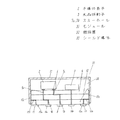
以下、本実施の形態について図面を用いて説明する。図1は本実施の形態におけるモジュールの断面図である。図1において本実施の形態におけるモジュール1では、半導体素子2や水晶振動子3などの複数個の電子部品が基板4の表面に実装され、基板4上に高周波回路が形成されている。基板4の表側にはシールドカバー5(シールド導体の一例として用いた)が装着され、シールドカバー5がこれらの電子部品を覆う構造を有している。なお、本実施の形態において基板4には、4層の多層基板を用いている。
(Embodiment 1)
Hereinafter, the present embodiment will be described with reference to the drawings. FIG. 1 is a cross-sectional view of a module in the present embodiment. In FIG. 1, in the
半導体素子2のグランド端子は、ハンダバンプによって基板4の表面に設けられたグランドパターン6へと接続されている。このグランドパターン6は、スルーホール7a、7bを経由して基板4の裏面に設けられたグランド端子8に接続される。なお、本実施の形態において、基板4の2層目はグランド層であり、この層には中継グランドが設けられている。この中継グランドとグランドパターンとの間はスルーホール7aによって接続され、中継グランドとグランド端子8との間はスルーホール7bによって接続されている。また水晶振動子3や他の一部の電子部品のグランド端子も同様にスルーホール(図示せず)によって中継グランドへと接続されている。
The ground terminal of the semiconductor element 2 is connected to a ground pattern 6 provided on the surface of the substrate 4 by solder bumps. The ground pattern 6 is connected to a
一方、半導体素子2の信号端子は、スルーホール9a、9bを介して基板4の裏面に設けられた信号端子10aへと接続される。なお、本実施の形態において第3層目は信号線を配線する層であり、この層には中継パターンが設けられている。この中継パターンと表面との間はスルーホール9aによって接続され、中継パターンと信号端子10aとの間はスルーホール9bによって接続されている。このように中継パターンを用いることにより、狭いピッチの半導体素子を用いることができる。また、一部の電子部品の信号端子は、基板4を全貫通するスルーホール(図示せず)を介して、基板4の裏面に設けられた信号端子10bに接続されている。つまり中継パターンを介さないで接続されるので、信号線の距離を最短の距離で接続することができる。従って、高周波信号の損失を小さくできる。さらに、他のパターンとの結合容量を小さくできるので、ノイズがスルーホール9a、9bに飛び込み難くなり、信号端子10bからノイズ信号などの不要な信号が出力されにくくなる。シールド端子11は、基板における裏面の周辺部に配置され、電気的にはシールドカバー5に対してのみ接続されている。ここでシールド端子11は複数個のシールド端子11が断続的に配置されることで形成される。そしてこれらのシールド端子11に囲まれた領域に、グランド端子8、信号端子10a、信号端子10bが配置される。ここで、これらシールド端子11同士の間には、シールド端子11同士の間隔は、モジュール1で使用する信号の中で最も高い周波数の信号における波長の長さの1/4以下の間隔としておく。これにより、高周波信号がモジュール1の外へ漏れ、外部機器へ影響などを与え難くなる。
On the other hand, the signal terminal of the semiconductor element 2 is connected to the
なお本実施の形態では、シールド端子11、グランド端子8、信号端子10a、信号端子10bとは全て同じ形状、同じ大きさとしたが、これは異なる大きさや、形状としても良い。また、シールド端子11をロの字やコの字、あるいはI字形状としても良い。
In this embodiment, the shield terminal 11, the
接続導体12は、シールド端子11とシールドカバー5との間を接続する。本実施の形態において接続導体12は、シールド端子11と接続されたスルーホール12aと、このスルーホール12aに接続された中継パターン12bと、この中継パターン12bに接続された接続部12cとから形成される。ここで、接続部12cは、基板4の側面に設けられた切り欠きの内周面に形成される。この切り欠きには、シールドカバー5の側面から延在して形成された脚5aが挿入され、この脚5aと接続部12cとの間が導電性の接続部材によって接続されている。なお、本実施の形態において接続部材には鉛フリーのはんだを用いている。また、本実施の形態では中継パターン12bは基板4の第3層目に設けたが、これは基板4の表面層や他の内層に設けても良い。さらに、接続部12cは基板4の側面に設けたが、これは基板4の表面側に設けても良い。なおこの場合脚5aは、接続部12cと対向するようにシールドカバー5の側面から折り曲げて形成される。
The connection conductor 12 connects between the shield terminal 11 and the shield cover 5. In the present embodiment, the connection conductor 12 is formed of a through
以上のような構成においてシールドカバー5は接続導体12を経由してシールド端子11とのみ接続されている。またこのシールド端子11は中継パターン12bを介し他のシールド端子11に接続される。ここで、シールド端子11や接続導体12は共に、半導体素子2などの電子部品のグランド端子、グランドパターン6や中継グランド、スルーホール7a、スルーホール7bさらにはグランド端子8とは基板4のなかでは互いに分離され独立して相互に接続されていない。
In the above configuration, the shield cover 5 is connected only to the shield terminal 11 via the connection conductor 12. The shield terminal 11 is connected to another shield terminal 11 via the relay pattern 12b. Here, the shield terminal 11 and the connection conductor 12 are both the ground terminal of the electronic component such as the semiconductor element 2, the ground pattern 6, the relay ground, the through hole 7 a, the through hole 7 b, and the
以上のような構成により、基板4に実装された半導体素子2や水晶振動子3などの電子部品のグランドとシールドカバー5とが、基板4内で接続されることがない。これにより、シールドカバーはより電位がゼロに近づき、安定したグランドをとることができる。これにより、モジュール1のシールド性が向上し、半導体素子2や水晶振動子3などの電子部品が発するノイズの漏洩や放射を低減できる。また、逆に外来のノイズがモジュール1内の高周波回路へ飛び込みにくくできる。更に、このようにシールド性が強化されることにより、グランド導体は小さくてもノイズの放射などが少なくできるので、グランド導体を小型化できる。従って、モジュール1を小型化することもできる。
With the configuration described above, the ground of the electronic component such as the semiconductor element 2 or the crystal resonator 3 mounted on the substrate 4 and the shield cover 5 are not connected in the substrate 4. As a result, the potential of the shield cover approaches zero and a stable ground can be obtained. Thereby, the shielding performance of the
さらにまた、スルーホール12a同士の間隔も使用する高周波信号の波長の長さの1/4以下の間隔で形成されることとなるので、高周波信号がモジュール1の外へ漏れ、外部機器へ影響などを与え難くなる。
Furthermore, since the interval between the through
図2は、本実施の形態における電子機器の要部断面図である。図3はモジュール1の裏面電極を示す平面図である。図2において、本実施の形態における電子機器21は、マザー基板22の上面にモジュール1が装着されている。マザー基板22の上面には、グランド端子8、信号端子10a、信号端子10b、シールド端子11のそれぞれと対応する位置に接続ランドが設けられている。ここで、モジュール1において、隣接したシールド端子11の間にシールド端子11の不形成部を設けておく。これにより、マザー基板22においてこの不形成部と対応する位置は、接続ランドが形成されない。従って、シールド端子11に対応する接続ランドの間を通して配線パターンを形成できる。
FIG. 2 is a cross-sectional view of a main part of the electronic device according to the present embodiment. FIG. 3 is a plan view showing the back electrode of the
(実施の形態2)
以下、本実施の形態について図面を用いて説明する。図4は、本実施の形態におけるモジュールの断面図である。図4において、図1と同じものには、同じ番号を用いて、その説明は簡略化している。
(Embodiment 2)
Hereinafter, the present embodiment will be described with reference to the drawings. FIG. 4 is a cross-sectional view of the module in the present embodiment. 4, the same components as those in FIG. 1 are denoted by the same reference numerals, and the description thereof is simplified.
図4において、本実施の形態におけるモジュール31は、実施の形態1におけるモジュール1に対し、基板4の表面側には樹脂層32が形成され、この樹脂層32内に半導体素子2や水晶振動子3を含む電子部品が埋設されている。なお、本実施の形態では、樹脂層32の側面と基板4の側面と一直線上にならぶように形成されている。
In FIG. 4, the
さらに、本実施の形態におけるモジュール31では、シールドカバー5に代えてシールド導体33が形成されている。このシールド導体33は、樹脂層32の上面ならびに側面、さらに基板4の側面の全面に形成されている。これにより、モジュール31は基板4の裏面以外がシールド導体33でシールドされる。従って、さらにシールド性が良好なモジュールを実現できる。
Further, in the
なお本実施の形態におけるシールド導体33は、めっきにより形成されているが、これは銀ペーストなどのような導体ペーストによって形成しても良い。このようにすれば、シールド導体33の形成がメッキに比べ容易であり、生産性が良好なモジュールを実現できる。
Although the
また、本実施の形態では基板側面の全面にシールド導体33を形成したが、基板4の側面の一部にシールド導体33の不形成部を設けても良い。このようにすれば、シールド導体33の不形成部同士で複数個の基板4を連結した状態で、半導体素子2や水晶振動子3などの電子部品の実装や、樹脂層32の形成、さらにはシールド導体33のメッキ作業を行うことができるので、非常に生産性が良好なモジュールを得ることができる。
In the present embodiment, the
本発明にかかる高周波モジュールは、シールド性が良好であるという効果を有し、高周波回路が搭載されたモジュール等に用いると有用である。 The high-frequency module according to the present invention has an effect of good shielding properties, and is useful when used for a module or the like on which a high-frequency circuit is mounted.
1 モジュール
2 半導体素子
3 水晶振動子
4 基板
5 シールドカバー
5a 脚
6 グランドパターン
7a スルーホール
7b スルーホール
8 グランド端子
9a スルーホール
9b スルーホール
10a 信号端子
10b 信号端子
11 シールド端子
12 接続導体
12a スルーホール
12b 中継パターン
12c 接続部
21 電子機器
22 マザー基板
31 モジュール
32 樹脂層
33 シールド導体
DESCRIPTION OF
Claims (2)
Priority Applications (1)
| Application Number | Priority Date | Filing Date | Title |
|---|---|---|---|
| JP2008057452A JP5146019B2 (en) | 2008-03-07 | 2008-03-07 | High frequency module and electronic device using the same |
Applications Claiming Priority (1)
| Application Number | Priority Date | Filing Date | Title |
|---|---|---|---|
| JP2008057452A JP5146019B2 (en) | 2008-03-07 | 2008-03-07 | High frequency module and electronic device using the same |
Publications (2)
| Publication Number | Publication Date |
|---|---|
| JP2009218258A JP2009218258A (en) | 2009-09-24 |
| JP5146019B2 true JP5146019B2 (en) | 2013-02-20 |
Family
ID=41189865
Family Applications (1)
| Application Number | Title | Priority Date | Filing Date |
|---|---|---|---|
| JP2008057452A Expired - Fee Related JP5146019B2 (en) | 2008-03-07 | 2008-03-07 | High frequency module and electronic device using the same |
Country Status (1)
| Country | Link |
|---|---|
| JP (1) | JP5146019B2 (en) |
Families Citing this family (4)
| Publication number | Priority date | Publication date | Assignee | Title |
|---|---|---|---|---|
| JP6508920B2 (en) | 2014-11-13 | 2019-05-08 | 太陽誘電株式会社 | Elastic wave device and transmission / reception device |
| JP6593556B2 (en) | 2017-01-27 | 2019-10-23 | 株式会社村田製作所 | Interposer substrate, circuit module, and method of manufacturing interposer substrate |
| WO2019045088A1 (en) * | 2017-09-04 | 2019-03-07 | 株式会社村田製作所 | High frequency module and method for producing same |
| KR20220164305A (en) * | 2021-06-04 | 2022-12-13 | 삼성전자주식회사 | Shield structure in an electronic devices and method thereof |
-
2008
- 2008-03-07 JP JP2008057452A patent/JP5146019B2/en not_active Expired - Fee Related
Also Published As
| Publication number | Publication date |
|---|---|
| JP2009218258A (en) | 2009-09-24 |
Similar Documents
| Publication | Publication Date | Title |
|---|---|---|
| JPWO2018164158A1 (en) | High frequency module | |
| US8102669B2 (en) | Chip package structure with shielding cover | |
| JP5750528B1 (en) | Circuit board with built-in components | |
| US20080003846A1 (en) | Circuit board unit | |
| JP2014027559A (en) | Ebg structure and circuit board | |
| JP5146019B2 (en) | High frequency module and electronic device using the same | |
| JP6973667B2 (en) | Circuit boards and electronic devices | |
| CN110506454B (en) | Connection structure between substrates | |
| JP2007059533A (en) | Circuit module | |
| JPWO2006093155A1 (en) | Board-to-board connector and circuit board device using board-to-board connector | |
| EP1594353A1 (en) | High frequency multilayer printed wiring board | |
| CN1972561A (en) | Pcb | |
| JP2015176966A (en) | Electronic device | |
| JP5577716B2 (en) | Circuit module and method for manufacturing circuit module | |
| JP2006211620A (en) | Filter and duplexer | |
| JPWO2008010445A1 (en) | Multilayer printed circuit board | |
| JP2008112832A (en) | High-frequency unit, and manufacturing method of high-frequency unit | |
| JP2007042957A (en) | Method for partially plating multilayer substrate for semiconductor device | |
| JP2014053445A (en) | Circuit board and composite module | |
| JP2008034672A (en) | Method for mounting chip component, and electronic module | |
| US7414321B2 (en) | Wiring configuration for semiconductor component | |
| JP2008124167A (en) | High-frequency module and electronic equipment using the same | |
| JP2004056155A (en) | Modular component | |
| US20070089901A1 (en) | Circuit board providing coplanarity of solders and high soldering reliability for semiconductor component | |
| JP2011108719A (en) | High frequency device |
Legal Events
| Date | Code | Title | Description |
|---|---|---|---|
| A621 | Written request for application examination |
Free format text: JAPANESE INTERMEDIATE CODE: A621 Effective date: 20100308 |
|
| RD01 | Notification of change of attorney |
Free format text: JAPANESE INTERMEDIATE CODE: A7421 Effective date: 20100413 |
|
| A977 | Report on retrieval |
Free format text: JAPANESE INTERMEDIATE CODE: A971007 Effective date: 20111031 |
|
| A131 | Notification of reasons for refusal |
Free format text: JAPANESE INTERMEDIATE CODE: A131 Effective date: 20111115 |
|
| A521 | Written amendment |
Free format text: JAPANESE INTERMEDIATE CODE: A523 Effective date: 20111213 |
|
| A131 | Notification of reasons for refusal |
Free format text: JAPANESE INTERMEDIATE CODE: A131 Effective date: 20120626 |
|
| A521 | Written amendment |
Free format text: JAPANESE INTERMEDIATE CODE: A523 Effective date: 20120801 |
|
| TRDD | Decision of grant or rejection written | ||
| A01 | Written decision to grant a patent or to grant a registration (utility model) |
Free format text: JAPANESE INTERMEDIATE CODE: A01 Effective date: 20121030 |
|
| A61 | First payment of annual fees (during grant procedure) |
Free format text: JAPANESE INTERMEDIATE CODE: A61 Effective date: 20121112 |
|
| FPAY | Renewal fee payment (prs date is renewal date of database) |
Free format text: PAYMENT UNTIL: 20151207 Year of fee payment: 3 |
|
| LAPS | Cancellation because of no payment of annual fees |