JP5627210B2 - 画像形成装置 - Google Patents
画像形成装置 Download PDFInfo
- Publication number
- JP5627210B2 JP5627210B2 JP2009216953A JP2009216953A JP5627210B2 JP 5627210 B2 JP5627210 B2 JP 5627210B2 JP 2009216953 A JP2009216953 A JP 2009216953A JP 2009216953 A JP2009216953 A JP 2009216953A JP 5627210 B2 JP5627210 B2 JP 5627210B2
- Authority
- JP
- Japan
- Prior art keywords
- image
- transfer
- primary transfer
- current
- constant current
- Prior art date
- Legal status (The legal status is an assumption and is not a legal conclusion. Google has not performed a legal analysis and makes no representation as to the accuracy of the status listed.)
- Expired - Fee Related
Links
Images


Classifications
-
- G—PHYSICS
- G03—PHOTOGRAPHY; CINEMATOGRAPHY; ANALOGOUS TECHNIQUES USING WAVES OTHER THAN OPTICAL WAVES; ELECTROGRAPHY; HOLOGRAPHY
- G03G—ELECTROGRAPHY; ELECTROPHOTOGRAPHY; MAGNETOGRAPHY
- G03G15/00—Apparatus for electrographic processes using a charge pattern
- G03G15/14—Apparatus for electrographic processes using a charge pattern for transferring a pattern to a second base
- G03G15/16—Apparatus for electrographic processes using a charge pattern for transferring a pattern to a second base of a toner pattern, e.g. a powder pattern, e.g. magnetic transfer
- G03G15/1605—Apparatus for electrographic processes using a charge pattern for transferring a pattern to a second base of a toner pattern, e.g. a powder pattern, e.g. magnetic transfer using at least one intermediate support
-
- G—PHYSICS
- G03—PHOTOGRAPHY; CINEMATOGRAPHY; ANALOGOUS TECHNIQUES USING WAVES OTHER THAN OPTICAL WAVES; ELECTROGRAPHY; HOLOGRAPHY
- G03G—ELECTROGRAPHY; ELECTROPHOTOGRAPHY; MAGNETOGRAPHY
- G03G15/00—Apparatus for electrographic processes using a charge pattern
- G03G15/14—Apparatus for electrographic processes using a charge pattern for transferring a pattern to a second base
- G03G15/16—Apparatus for electrographic processes using a charge pattern for transferring a pattern to a second base of a toner pattern, e.g. a powder pattern, e.g. magnetic transfer
- G03G15/1665—Apparatus for electrographic processes using a charge pattern for transferring a pattern to a second base of a toner pattern, e.g. a powder pattern, e.g. magnetic transfer by introducing the second base in the nip formed by the recording member and at least one transfer member, e.g. in combination with bias or heat
- G03G15/167—Apparatus for electrographic processes using a charge pattern for transferring a pattern to a second base of a toner pattern, e.g. a powder pattern, e.g. magnetic transfer by introducing the second base in the nip formed by the recording member and at least one transfer member, e.g. in combination with bias or heat at least one of the recording member or the transfer member being rotatable during the transfer
- G03G15/1675—Apparatus for electrographic processes using a charge pattern for transferring a pattern to a second base of a toner pattern, e.g. a powder pattern, e.g. magnetic transfer by introducing the second base in the nip formed by the recording member and at least one transfer member, e.g. in combination with bias or heat at least one of the recording member or the transfer member being rotatable during the transfer with means for controlling the bias applied in the transfer nip
Landscapes
- Physics & Mathematics (AREA)
- General Physics & Mathematics (AREA)
- Electrostatic Charge, Transfer And Separation In Electrography (AREA)
- Control Or Security For Electrophotography (AREA)
Description
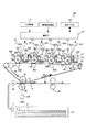
図1は画像形成装置の構成の説明図である。図1に示すように、画像形成装置100は、中間転写ベルト30に沿ってイエロー、マゼンタ、シアン、ブラックの画像形成部PY、PM、PC、PKを配列したタンデム型中間転写方式のフルカラープリンタである。画像形成装置100における、A4プリント速度は、60ppm(枚/分)である。
ここで、一次転写部(TY)における一次転写ローラ60Y、中間転写ベルト30、一次転写部(TY)、感光ドラム17Yのインピーダンスを加算した値を一次転写部のトータルインピーダンスと定義する。
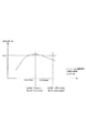
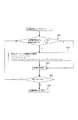
図2は実施例2における定電流制御の構成の説明図である。図3は一次転写ローラの新品状態と耐久状態とにおける転写コントラストの違いの説明図である。図4は画像形成の累積に伴う一次転写部のトータルインピーダンスの変化の説明図である。図5は画像部を流れる転写電流と転写効率の関係の説明図である。図6は一次転写部のトータルインピーダンスの上昇に伴う一次転写電流密度の変化の説明図である。図7は実施例1の制御のフローチャートである。
Is_Im=1TRc_IM/((30cm/5cm)*RA)=12.5μA
Is_W=1TRc_W/((30cm/25cm)*RA)=112.5μA
Is_Im´=1TRc_IM´/((30cm/5cm)*RA´)=19.2μA
Is_W´=1TRc_W´/((30cm/25cm)*RA´)=105.8μA
1TRV´=125μA×RA(1)−(25cm*Vd+5cm*VL)/30cm
={125μA×6RA(1)−(5Vd+VL)}/6=1050V
Is_Im´ =(1TRV´+VL)/(30cm/5cm)RA(1)=14.88μA
Is_Imd´=Is_Im´/5cm=2.976μA/cm
1TRV(1)=(Is_Imd×5cm×(30cm/5cm)・RA(1))−VL=850V
Is_W(1)=(1TRV(1)+Vd)/(30cm/25cm)*RA(1)=98.21μA
Is(1)=Is_Im(1)+Is_W(1)=12.5μA+98.21μA=110.71μA≒110μA
(1)感光ドラム上17Y上に全面ベタ白画像を形成する。
(2)定電流制御の一次転写ターゲット電流値:Is(n−1)μAを印加したときの全面ベタ白画像の一次転写コントラストを求める。
(3)全面ベタ白画像の一次転写コントラストと一次転写ターゲット電流値とにより一次転写部TYのトータルインピーダンス:RA(n)を求める。
(4)定電流制御における一次転写ターゲット電流値:Is(n)を求める。
Is(n)=I_Im(n)+Is_W(n)
=Is_Imd×5cm+{(Is_Imd×5cm×(30cm/5cm)・RA(n))−VL+Vd)/((30cm/25cm)・RA(n))}
Is(n)=Is_Im(n)+Is_W(n)
=Is_Imd×P+{(Is_Imd×P×((P+Q)/P)・RA(n))−VL+Vd)/(((P+Q)/Q)・RA(n))}
図8は実施例2における定電流制御の構成の説明図である。図9は潜像コントラストが大きい状態と小さい状態とにおける転写コントラストの違いの説明図である。図10は画像部を流れる転写電流と転写効率の関係の説明図である。図11は実施例2の制御のフローチャートである。
Is_Im=1TRc_IM/((30cm/5cm)*RA)=12.5μA
Is_W =1TRc_W/((30cm/25cm)*RA)=112.5μA
Is_Im´=1TRc_IM´/((30cm/5cm)*RA)=18.7μA
Is_W´ =1TRc_W´/((30cm/25cm)*RA)=108.3μA
Is_Imd =12.5μA/5cm=2.5(μA/cm)
Is_Imd´=18.7μA/5cm=3.33(μA/cm)
1TRV(1)=(Is_Imd×5cm×(30cm/5cm)・RA)−VL´=450V
Is_W(1)=(1TRV(1)+Vd´)/(30cm/25cm)・RA=87.5μA
Is(1)=Is_Im(1)+Is_W(1)=12.5μA+87.5μA=100μA
Is(n)=Is_Im(n)+Is_W(n)
=Is_Imd×P+{(Is_Imd×P×((P+Q)/P)・RA)−VL´+Vd´)/(((P+Q)/Q)・RA)}
図12は実施例3における定電流制御の構成の説明図である。図13は空気中の絶対水分量が少ない状態と多い状態とにおける転写コントラストの違いの説明図である。図14は空気中の絶対水分量と一次転写部のトータルインピーダンスの関係の説明図である。図15は画像部を流れる転写電流と転写効率の関係の説明図である。図16は実施例3の制御のフローチャートである。
Is_Im=1TRc_IM/((30cm/5cm)*RA)=12.5μA
Is_W =1TRc_W/((30cm/25cm)*RA)=72.5μA
Is_Im´=1TRc_IM´/((30cm/5cm)*RA´)=5.83μA
Is_W´ =1TRc_W´/((30cm/25cm)*RA´)=79.1μA
10.0(g/kg):Is_Imd =12.5μA/5cm=2.5(μA/cm)
20.0(g/kg):Is_Imd´=5.83μA/5cm=1.16(μA/cm)
1TRV(Ha´)=(Is_Imd×5cm×((30cm/5cm)・RA(Ha´)))−VL=750V
Is_W(Ha´)=(1TRV(Ha´)+Vd)/((30cm/25cm)RA(Ha´))=112.5μA
Is(Ha´)=Is_Im(Ha´)+Is_W(Ha´)=12.5μA+112.5μA=125μA
Is(Ha)=Is_Im(Ha)+Is_W(Ha)
=Is_Imd×P+{((Is_Imd×P×((P+Q)/P)・RA(Ha))−VL+Vd)/(((P+Q)/Q)・RA(Ha))}
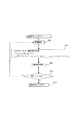
図17は実施例4の画像形成装置の構成の説明図である。図17に示すように、画像形成装置200は、感光ドラム17より記録材Pへ直接に転写を行う単色のレーザービームプリンタである。
18Y、18M、18C、18K 露光手段(露光装置)
19Y、19M、19C、19K 帯電手段(コロナ帯電器)
20Y、20M、20C、20K 現像手段(現像装置)
30 中間転写体(中間転写ベルト)
60Y、60M、60C、60K 転写部材(一次転写ローラ)
65 一次転写バイアス印加部、67 定電流制御回路、
68 電流設定手段(設定一次転写ターゲット電流値設定部)
69 一次転写印加バイアスモニタ部、75 電位測定部、76 環境センサ
90Y、90M、90C、90K 電位センサ
110 制御部
P 記録材
PY、PM、PC、PK 画像形成部
TY、TM、TC、TK 一次転写部
Claims (6)
- 感光体と、
前記感光体を帯電させる帯電手段と、
非露光部電位に帯電された前記感光体を露光して露光部電位の静電像を形成する露光手段と、
前記静電像にトナーを付着させてトナー像に現像する現像手段と、
前記感光体との間に転写媒体を挟持してトナー像の転写部を形成する転写部材と、
前記転写部材に電圧を印加してトナー像を転写媒体へ転写させる定電流制御された電源と、
前記転写部の長手方向に沿った画像比率が第1の画像比率の場合の前記定電流制御の電流値を、前記第1の画像比率より低い第2の画像比率の場合の前記定電流制御の電流値より低く設定する電流設定手段と、を備える画像形成装置において、
前記電流設定手段は、トナー像の転写時に前記転写部材に印加する電圧と前記感光体の表面電位との電位差を転写コントラストとするとき、前記非露光部の転写コントラストに対する前記露光部の転写コントラストの比率が第1の比率の場合の前記定電流制御の電流値を、前記第1の比率より低い第2の比率の場合の前記定電流制御の電流値より低く設定することを特徴とする画像形成装置。 - 画像形成装置内の温度と湿度を検知する検知部材を備え、
前記電流設定手段は、前記検知部材の検知結果により空気中の水分量が第1の水分量の場合の前記定電流制御の電流値を、前記第1の水分量より高い第2の水分量の場合の前記定電流制御の電流値より低く設定することを特徴とする請求項1に記載の画像形成装置。 - 前記電流設定手段は、前記転写部材の抵抗値が第1の抵抗値の場合の前記定電流制御の電流値を、前記第1の抵抗値より低い第2の抵抗値の場合の前記定電流制御の電流値より低く設定することを特徴とする請求項1に記載の画像形成装置。
- 前記転写部材に印加する電圧を検出する電圧検出手段を備え、
前記電流設定手段は、非画像形成時に所定の電流値で定電流制御された電圧を前記転写部材に印加させる電圧検出モードを実行し、前記電圧検出モードで前記電圧検出手段が検出した電圧が第1の電圧の場合の前記定電流制御の電流値を、前記第1の電圧より低い第2の電圧の場合の前記定電流制御の電流値より低く設定することを特徴とする請求項1に記載の画像形成装置。 - 前記電流設定手段は、前記非露光部電位と前記露光部電位との電位差の絶対値が第1の電位差の場合の前記定電流制御の電流値を、前記第1の電位差の絶対値より高い第2の電位差の絶対値の場合の前記定電流制御の電流値より低く設定することを特徴とする請求項1に記載の画像形成装置。
- 前記感光体に対向配置されて前記非露光部電位と前記露光部電位とを検出可能な電位センサを備え、
前記電流設定手段は、前記電位センサの出力に基づいて前記定電流制御の電流値を設定することを特徴とする請求項5に記載の画像形成装置。
Priority Applications (3)
| Application Number | Priority Date | Filing Date | Title |
|---|---|---|---|
| JP2009216953A JP5627210B2 (ja) | 2009-09-18 | 2009-09-18 | 画像形成装置 |
| US12/873,686 US8831452B2 (en) | 2009-09-18 | 2010-09-01 | Image forming apparatus with transfer voltage detection |
| CN2010102844872A CN102023537B (zh) | 2009-09-18 | 2010-09-17 | 图像形成设备 |
Applications Claiming Priority (1)
| Application Number | Priority Date | Filing Date | Title |
|---|---|---|---|
| JP2009216953A JP5627210B2 (ja) | 2009-09-18 | 2009-09-18 | 画像形成装置 |
Publications (3)
| Publication Number | Publication Date |
|---|---|
| JP2011065024A JP2011065024A (ja) | 2011-03-31 |
| JP2011065024A5 JP2011065024A5 (ja) | 2012-11-01 |
| JP5627210B2 true JP5627210B2 (ja) | 2014-11-19 |
Family
ID=43756711
Family Applications (1)
| Application Number | Title | Priority Date | Filing Date |
|---|---|---|---|
| JP2009216953A Expired - Fee Related JP5627210B2 (ja) | 2009-09-18 | 2009-09-18 | 画像形成装置 |
Country Status (3)
| Country | Link |
|---|---|
| US (1) | US8831452B2 (ja) |
| JP (1) | JP5627210B2 (ja) |
| CN (1) | CN102023537B (ja) |
Families Citing this family (16)
| Publication number | Priority date | Publication date | Assignee | Title |
|---|---|---|---|---|
| JP6032519B2 (ja) * | 2011-11-08 | 2016-11-30 | 株式会社リコー | 画像形成装置 |
| JP5892413B2 (ja) * | 2011-11-18 | 2016-03-23 | 株式会社リコー | 画像形成装置 |
| JP5723852B2 (ja) | 2012-10-31 | 2015-05-27 | 京セラドキュメントソリューションズ株式会社 | 転写装置、及びこれを備えた画像形成装置 |
| JP5808312B2 (ja) * | 2012-11-28 | 2015-11-10 | 株式会社沖データ | 画像形成装置 |
| JP6184197B2 (ja) * | 2013-06-26 | 2017-08-23 | キヤノン株式会社 | 画像形成装置 |
| JP6168910B2 (ja) * | 2013-08-19 | 2017-07-26 | キヤノン株式会社 | 画像形成装置 |
| JP6335648B2 (ja) | 2014-05-23 | 2018-05-30 | キヤノン株式会社 | 画像形成装置 |
| JP2016057582A (ja) * | 2014-09-12 | 2016-04-21 | キヤノン株式会社 | 画像形成装置 |
| JP6204317B2 (ja) * | 2014-09-16 | 2017-09-27 | 京セラドキュメントソリューションズ株式会社 | 画像形成装置 |
| JP2016126050A (ja) * | 2014-12-26 | 2016-07-11 | ブラザー工業株式会社 | 画像形成装置、制御方法およびプログラム |
| JP6699278B2 (ja) * | 2016-03-23 | 2020-05-27 | 富士ゼロックス株式会社 | 転写装置、転写プログラム、及び画像形成装置 |
| JP6794665B2 (ja) * | 2016-06-02 | 2020-12-02 | 富士ゼロックス株式会社 | 画像形成装置 |
| JP2018116223A (ja) * | 2017-01-20 | 2018-07-26 | キヤノン株式会社 | 画像形成装置 |
| JP7005197B2 (ja) * | 2017-07-07 | 2022-01-21 | キヤノン株式会社 | 画像形成装置 |
| EP3438755B1 (en) * | 2017-08-04 | 2022-06-22 | Canon Kabushiki Kaisha | Image forming apparatus |
| US11143989B2 (en) * | 2018-08-09 | 2021-10-12 | Canon Kabushiki Kaisha | Image forming apparatus |
Family Cites Families (11)
| Publication number | Priority date | Publication date | Assignee | Title |
|---|---|---|---|---|
| JPH0883006A (ja) * | 1994-09-09 | 1996-03-26 | Ricoh Co Ltd | 画像形成装置 |
| JP2000075687A (ja) | 1998-08-31 | 2000-03-14 | Canon Inc | 転写装置および画像形成装置 |
| JP2002278176A (ja) * | 2001-03-14 | 2002-09-27 | Canon Inc | 画像形成装置 |
| JP4500511B2 (ja) | 2002-07-03 | 2010-07-14 | キヤノン株式会社 | 画像形成装置 |
| US7340191B2 (en) * | 2004-03-04 | 2008-03-04 | Canon Kabushiki Kaisha | Image forming apparatus featuring variably-controlling a primary-transferring condition based on a detection result of combined toner images |
| JP2006126320A (ja) * | 2004-10-27 | 2006-05-18 | Canon Inc | 画像形成装置 |
| JP2006251204A (ja) * | 2005-03-09 | 2006-09-21 | Toshiba Corp | 画像形成装置 |
| JP5127205B2 (ja) * | 2006-11-22 | 2013-01-23 | キヤノン株式会社 | 画像形成装置 |
| US7742712B2 (en) * | 2007-01-29 | 2010-06-22 | Kabushiki Kaisha Toshiba | Transfer bias voltage controlling apparatus |
| JP2008268385A (ja) * | 2007-04-17 | 2008-11-06 | Ricoh Co Ltd | 画像形成装置 |
| JP2008275844A (ja) * | 2007-04-27 | 2008-11-13 | Canon Inc | 画像形成装置 |
-
2009
- 2009-09-18 JP JP2009216953A patent/JP5627210B2/ja not_active Expired - Fee Related
-
2010
- 2010-09-01 US US12/873,686 patent/US8831452B2/en not_active Expired - Fee Related
- 2010-09-17 CN CN2010102844872A patent/CN102023537B/zh not_active Expired - Fee Related
Also Published As
| Publication number | Publication date |
|---|---|
| CN102023537B (zh) | 2013-06-05 |
| JP2011065024A (ja) | 2011-03-31 |
| CN102023537A (zh) | 2011-04-20 |
| US20110069979A1 (en) | 2011-03-24 |
| US8831452B2 (en) | 2014-09-09 |
Similar Documents
| Publication | Publication Date | Title |
|---|---|---|
| JP5627210B2 (ja) | 画像形成装置 | |
| US8000640B2 (en) | Image forming apparatus | |
| US9454109B2 (en) | Image forming apparatus controlling transfer conditions based on resistance of transfer member | |
| JP2007079071A (ja) | 画像形成装置 | |
| JP5653406B2 (ja) | 画像形成装置 | |
| JP4110035B2 (ja) | 画像形成装置 | |
| JP2017068128A (ja) | 画像形成装置 | |
| JP2004280069A (ja) | 画像形成装置 | |
| JP2013171094A (ja) | 画像形成装置 | |
| JP6859085B2 (ja) | 画像形成装置 | |
| WO2018101486A1 (ja) | 画像形成装置 | |
| US7466933B2 (en) | Image forming apparatus in which reverse transfer of a developing agent is prevented | |
| JP6887978B2 (ja) | 画像形成装置 | |
| JP2016161932A (ja) | 画像形成装置 | |
| JP2009058869A (ja) | 画像形成装置 | |
| JPH10221931A (ja) | 画像形成装置 | |
| JP2021009210A (ja) | 画像形成装置 | |
| JP2004334017A (ja) | 画像形成装置 | |
| JP4631325B2 (ja) | 画像濃度調整装置、及びこれを用いた画像形成装置 | |
| JP2001005237A (ja) | 画像形成装置 | |
| JP5262622B2 (ja) | 画像形成装置 | |
| JP2018189797A (ja) | 画像形成装置 | |
| JP3308800B2 (ja) | 画像形成装置 | |
| JP2006243335A (ja) | 画像形成装置 | |
| JP2022082352A (ja) | 画像形成装置、画像形成装置の制御方法、及びプログラム |
Legal Events
| Date | Code | Title | Description |
|---|---|---|---|
| RD03 | Notification of appointment of power of attorney |
Free format text: JAPANESE INTERMEDIATE CODE: A7423 Effective date: 20120203 |
|
| A521 | Written amendment |
Free format text: JAPANESE INTERMEDIATE CODE: A523 Effective date: 20120918 |
|
| A621 | Written request for application examination |
Free format text: JAPANESE INTERMEDIATE CODE: A621 Effective date: 20120918 |
|
| RD04 | Notification of resignation of power of attorney |
Free format text: JAPANESE INTERMEDIATE CODE: A7424 Effective date: 20130228 |
|
| A977 | Report on retrieval |
Free format text: JAPANESE INTERMEDIATE CODE: A971007 Effective date: 20130903 |
|
| A131 | Notification of reasons for refusal |
Free format text: JAPANESE INTERMEDIATE CODE: A131 Effective date: 20130910 |
|
| A131 | Notification of reasons for refusal |
Free format text: JAPANESE INTERMEDIATE CODE: A131 Effective date: 20140408 |
|
| A521 | Written amendment |
Free format text: JAPANESE INTERMEDIATE CODE: A523 Effective date: 20140605 |
|
| TRDD | Decision of grant or rejection written | ||
| A01 | Written decision to grant a patent or to grant a registration (utility model) |
Free format text: JAPANESE INTERMEDIATE CODE: A01 Effective date: 20140902 |
|
| A61 | First payment of annual fees (during grant procedure) |
Free format text: JAPANESE INTERMEDIATE CODE: A61 Effective date: 20140930 |
|
| LAPS | Cancellation because of no payment of annual fees |