JP5521848B2 - 異方性導電フィルム、接続構造体及びそれらの製造方法 - Google Patents
異方性導電フィルム、接続構造体及びそれらの製造方法 Download PDFInfo
- Publication number
- JP5521848B2 JP5521848B2 JP2010164134A JP2010164134A JP5521848B2 JP 5521848 B2 JP5521848 B2 JP 5521848B2 JP 2010164134 A JP2010164134 A JP 2010164134A JP 2010164134 A JP2010164134 A JP 2010164134A JP 5521848 B2 JP5521848 B2 JP 5521848B2
- Authority
- JP
- Japan
- Prior art keywords
- meth
- acrylate
- anisotropic conductive
- conductive film
- electronic component
- Prior art date
- Legal status (The legal status is an assumption and is not a legal conclusion. Google has not performed a legal analysis and makes no representation as to the accuracy of the status listed.)
- Active
Links
- 238000004519 manufacturing process Methods 0.000 title claims description 13
- NIXOWILDQLNWCW-UHFFFAOYSA-M Acrylate Chemical compound [O-]C(=O)C=C NIXOWILDQLNWCW-UHFFFAOYSA-M 0.000 claims description 90
- 239000000853 adhesive Substances 0.000 claims description 48
- 230000001070 adhesive effect Effects 0.000 claims description 48
- 239000000203 mixture Substances 0.000 claims description 41
- 239000000178 monomer Substances 0.000 claims description 35
- 150000003950 cyclic amides Chemical group 0.000 claims description 17
- 239000002245 particle Substances 0.000 claims description 15
- 229920005989 resin Polymers 0.000 claims description 14
- 239000011347 resin Substances 0.000 claims description 14
- 125000002947 alkylene group Chemical group 0.000 claims description 13
- 125000002496 methyl group Chemical group [H]C([H])([H])* 0.000 claims description 10
- 125000004430 oxygen atom Chemical group O* 0.000 claims description 10
- 239000007870 radical polymerization initiator Substances 0.000 claims description 10
- 125000004435 hydrogen atom Chemical group [H]* 0.000 claims description 6
- 125000003545 alkoxy group Chemical group 0.000 claims description 5
- 125000000217 alkyl group Chemical group 0.000 claims description 4
- 125000003118 aryl group Chemical group 0.000 claims description 4
- 238000010438 heat treatment Methods 0.000 claims description 4
- 229910052799 carbon Inorganic materials 0.000 claims description 3
- 125000004432 carbon atom Chemical group C* 0.000 claims description 3
- 125000005843 halogen group Chemical group 0.000 claims description 3
- 229910052757 nitrogen Inorganic materials 0.000 claims description 3
- 125000004433 nitrogen atom Chemical group N* 0.000 claims description 3
- 229910052717 sulfur Inorganic materials 0.000 claims description 3
- 125000004434 sulfur atom Chemical group 0.000 claims description 3
- -1 dimethylene group Chemical group 0.000 description 16
- YXFVVABEGXRONW-UHFFFAOYSA-N Toluene Chemical compound CC1=CC=CC=C1 YXFVVABEGXRONW-UHFFFAOYSA-N 0.000 description 15
- XEKOWRVHYACXOJ-UHFFFAOYSA-N Ethyl acetate Chemical compound CCOC(C)=O XEKOWRVHYACXOJ-UHFFFAOYSA-N 0.000 description 9
- 229920001187 thermosetting polymer Polymers 0.000 description 8
- 230000015572 biosynthetic process Effects 0.000 description 7
- 230000000052 comparative effect Effects 0.000 description 7
- NIXOWILDQLNWCW-UHFFFAOYSA-N acrylic acid group Chemical group C(C=C)(=O)O NIXOWILDQLNWCW-UHFFFAOYSA-N 0.000 description 6
- 238000000034 method Methods 0.000 description 6
- 238000002156 mixing Methods 0.000 description 6
- 239000010949 copper Substances 0.000 description 5
- 239000010410 layer Substances 0.000 description 5
- 239000002184 metal Substances 0.000 description 5
- 229910052751 metal Inorganic materials 0.000 description 5
- 238000003786 synthesis reaction Methods 0.000 description 5
- 239000004593 Epoxy Substances 0.000 description 4
- 150000001252 acrylic acid derivatives Chemical class 0.000 description 4
- IISBACLAFKSPIT-UHFFFAOYSA-N bisphenol A Chemical compound C=1C=C(O)C=CC=1C(C)(C)C1=CC=C(O)C=C1 IISBACLAFKSPIT-UHFFFAOYSA-N 0.000 description 4
- 150000005676 cyclic carbonates Chemical group 0.000 description 4
- UHESRSKEBRADOO-UHFFFAOYSA-N ethyl carbamate;prop-2-enoic acid Chemical compound OC(=O)C=C.CCOC(N)=O UHESRSKEBRADOO-UHFFFAOYSA-N 0.000 description 4
- 239000011521 glass Substances 0.000 description 4
- 239000010931 gold Substances 0.000 description 4
- 125000002887 hydroxy group Chemical group [H]O* 0.000 description 4
- 239000013034 phenoxy resin Substances 0.000 description 4
- 229920006287 phenoxy resin Polymers 0.000 description 4
- FWIBCWKHNZBDLS-UHFFFAOYSA-N 3-hydroxyoxolan-2-one Chemical compound OC1CCOC1=O FWIBCWKHNZBDLS-UHFFFAOYSA-N 0.000 description 3
- PXHVJJICTQNCMI-UHFFFAOYSA-N Nickel Chemical compound [Ni] PXHVJJICTQNCMI-UHFFFAOYSA-N 0.000 description 3
- 239000002313 adhesive film Substances 0.000 description 3
- 238000000576 coating method Methods 0.000 description 3
- 230000018044 dehydration Effects 0.000 description 3
- 238000006297 dehydration reaction Methods 0.000 description 3
- 238000001035 drying Methods 0.000 description 3
- PCHJSUWPFVWCPO-UHFFFAOYSA-N gold Chemical compound [Au] PCHJSUWPFVWCPO-UHFFFAOYSA-N 0.000 description 3
- 229910052737 gold Inorganic materials 0.000 description 3
- 239000012046 mixed solvent Substances 0.000 description 3
- 150000001451 organic peroxides Chemical class 0.000 description 3
- 150000002978 peroxides Chemical class 0.000 description 3
- 125000001997 phenyl group Chemical group [H]C1=C([H])C([H])=C(*)C([H])=C1[H] 0.000 description 3
- 125000002467 phosphate group Chemical group [H]OP(=O)(O[H])O[*] 0.000 description 3
- 238000003825 pressing Methods 0.000 description 3
- 238000010526 radical polymerization reaction Methods 0.000 description 3
- 238000007363 ring formation reaction Methods 0.000 description 3
- 239000007787 solid Substances 0.000 description 3
- 239000004342 Benzoyl peroxide Substances 0.000 description 2
- OMPJBNCRMGITSC-UHFFFAOYSA-N Benzoylperoxide Chemical compound C=1C=CC=CC=1C(=O)OOC(=O)C1=CC=CC=C1 OMPJBNCRMGITSC-UHFFFAOYSA-N 0.000 description 2
- 229930185605 Bisphenol Natural products 0.000 description 2
- RYGMFSIKBFXOCR-UHFFFAOYSA-N Copper Chemical compound [Cu] RYGMFSIKBFXOCR-UHFFFAOYSA-N 0.000 description 2
- OKKJLVBELUTLKV-UHFFFAOYSA-N Methanol Chemical class OC OKKJLVBELUTLKV-UHFFFAOYSA-N 0.000 description 2
- KDLHZDBZIXYQEI-UHFFFAOYSA-N Palladium Chemical compound [Pd] KDLHZDBZIXYQEI-UHFFFAOYSA-N 0.000 description 2
- ZJCCRDAZUWHFQH-UHFFFAOYSA-N Trimethylolpropane Chemical compound CCC(CO)(CO)CO ZJCCRDAZUWHFQH-UHFFFAOYSA-N 0.000 description 2
- 235000019400 benzoyl peroxide Nutrition 0.000 description 2
- 230000001588 bifunctional effect Effects 0.000 description 2
- 229910052801 chlorine Inorganic materials 0.000 description 2
- 125000001309 chloro group Chemical group Cl* 0.000 description 2
- 239000011248 coating agent Substances 0.000 description 2
- 150000001875 compounds Chemical class 0.000 description 2
- 229910052802 copper Inorganic materials 0.000 description 2
- 125000001495 ethyl group Chemical group [H]C([H])([H])C([H])([H])* 0.000 description 2
- ZFSLODLOARCGLH-UHFFFAOYSA-N isocyanuric acid Chemical compound OC1=NC(O)=NC(O)=N1 ZFSLODLOARCGLH-UHFFFAOYSA-N 0.000 description 2
- 125000001570 methylene group Chemical group [H]C([H])([*:1])[*:2] 0.000 description 2
- 125000000896 monocarboxylic acid group Chemical group 0.000 description 2
- WXZMFSXDPGVJKK-UHFFFAOYSA-N pentaerythritol Chemical compound OCC(CO)(CO)CO WXZMFSXDPGVJKK-UHFFFAOYSA-N 0.000 description 2
- BNMMXDHVMLZQGP-UHFFFAOYSA-N phosphono prop-2-eneperoxoate Chemical compound OP(O)(=O)OOC(=O)C=C BNMMXDHVMLZQGP-UHFFFAOYSA-N 0.000 description 2
- 229920001721 polyimide Polymers 0.000 description 2
- 239000003505 polymerization initiator Substances 0.000 description 2
- 238000006116 polymerization reaction Methods 0.000 description 2
- 238000002360 preparation method Methods 0.000 description 2
- 239000004065 semiconductor Substances 0.000 description 2
- 229910000679 solder Inorganic materials 0.000 description 2
- 239000000126 substance Substances 0.000 description 2
- 125000001424 substituent group Chemical group 0.000 description 2
- 239000000758 substrate Substances 0.000 description 2
- JOXIMZWYDAKGHI-UHFFFAOYSA-N toluene-4-sulfonic acid Chemical compound CC1=CC=C(S(O)(=O)=O)C=C1 JOXIMZWYDAKGHI-UHFFFAOYSA-N 0.000 description 2
- 125000003258 trimethylene group Chemical group [H]C([H])([*:2])C([H])([H])C([H])([H])[*:1] 0.000 description 2
- BEQKKZICTDFVMG-UHFFFAOYSA-N 1,2,3,4,6-pentaoxepane-5,7-dione Chemical compound O=C1OOOOC(=O)O1 BEQKKZICTDFVMG-UHFFFAOYSA-N 0.000 description 1
- VZXTWGWHSMCWGA-UHFFFAOYSA-N 1,3,5-triazine-2,4-diamine Chemical compound NC1=NC=NC(N)=N1 VZXTWGWHSMCWGA-UHFFFAOYSA-N 0.000 description 1
- HECLRDQVFMWTQS-RGOKHQFPSA-N 1755-01-7 Chemical compound C1[C@H]2[C@@H]3CC=C[C@@H]3[C@@H]1C=C2 HECLRDQVFMWTQS-RGOKHQFPSA-N 0.000 description 1
- SMZOUWXMTYCWNB-UHFFFAOYSA-N 2-(2-methoxy-5-methylphenyl)ethanamine Chemical compound COC1=CC=C(C)C=C1CCN SMZOUWXMTYCWNB-UHFFFAOYSA-N 0.000 description 1
- TXBCBTDQIULDIA-UHFFFAOYSA-N 2-[[3-hydroxy-2,2-bis(hydroxymethyl)propoxy]methyl]-2-(hydroxymethyl)propane-1,3-diol Chemical compound OCC(CO)(CO)COCC(CO)(CO)CO TXBCBTDQIULDIA-UHFFFAOYSA-N 0.000 description 1
- 125000004493 2-methylbut-1-yl group Chemical group CC(C*)CC 0.000 description 1
- 125000003229 2-methylhexyl group Chemical group [H]C([H])([H])C([H])([H])C([H])([H])C([H])([H])C([H])(C([H])([H])[H])C([H])([H])* 0.000 description 1
- 125000003903 2-propenyl group Chemical group [H]C([*])([H])C([H])=C([H])[H] 0.000 description 1
- FRKGSNOMLIYPSH-UHFFFAOYSA-N 3-hydroxypyrrolidin-2-one Chemical group OC1CCNC1=O FRKGSNOMLIYPSH-UHFFFAOYSA-N 0.000 description 1
- YCIGYTFKOXGYTA-UHFFFAOYSA-N 4-(3-cyanopropyldiazenyl)butanenitrile Chemical compound N#CCCCN=NCCCC#N YCIGYTFKOXGYTA-UHFFFAOYSA-N 0.000 description 1
- JFMGYULNQJPJCY-UHFFFAOYSA-N 4-(hydroxymethyl)-1,3-dioxolan-2-one Chemical group OCC1COC(=O)O1 JFMGYULNQJPJCY-UHFFFAOYSA-N 0.000 description 1
- UZDMJPAQQFSMMV-UHFFFAOYSA-N 4-oxo-4-(2-prop-2-enoyloxyethoxy)butanoic acid Chemical compound OC(=O)CCC(=O)OCCOC(=O)C=C UZDMJPAQQFSMMV-UHFFFAOYSA-N 0.000 description 1
- BRLQWZUYTZBJKN-UHFFFAOYSA-N Epichlorohydrin Chemical compound ClCC1CO1 BRLQWZUYTZBJKN-UHFFFAOYSA-N 0.000 description 1
- JOYRKODLDBILNP-UHFFFAOYSA-N Ethyl urethane Chemical compound CCOC(N)=O JOYRKODLDBILNP-UHFFFAOYSA-N 0.000 description 1
- MHAJPDPJQMAIIY-UHFFFAOYSA-N Hydrogen peroxide Chemical compound OO MHAJPDPJQMAIIY-UHFFFAOYSA-N 0.000 description 1
- CERQOIWHTDAKMF-UHFFFAOYSA-M Methacrylate Chemical compound CC(=C)C([O-])=O CERQOIWHTDAKMF-UHFFFAOYSA-M 0.000 description 1
- NBIIXXVUZAFLBC-UHFFFAOYSA-N Phosphoric acid Chemical group OP(O)(O)=O NBIIXXVUZAFLBC-UHFFFAOYSA-N 0.000 description 1
- 239000002202 Polyethylene glycol Substances 0.000 description 1
- 239000004642 Polyimide Substances 0.000 description 1
- 239000004793 Polystyrene Substances 0.000 description 1
- 239000006087 Silane Coupling Agent Substances 0.000 description 1
- XUIMIQQOPSSXEZ-UHFFFAOYSA-N Silicon Chemical compound [Si] XUIMIQQOPSSXEZ-UHFFFAOYSA-N 0.000 description 1
- BQCADISMDOOEFD-UHFFFAOYSA-N Silver Chemical compound [Ag] BQCADISMDOOEFD-UHFFFAOYSA-N 0.000 description 1
- XRMBQHTWUBGQDN-UHFFFAOYSA-N [2-[2,2-bis(prop-2-enoyloxymethyl)butoxymethyl]-2-(prop-2-enoyloxymethyl)butyl] prop-2-enoate Chemical compound C=CC(=O)OCC(COC(=O)C=C)(CC)COCC(CC)(COC(=O)C=C)COC(=O)C=C XRMBQHTWUBGQDN-UHFFFAOYSA-N 0.000 description 1
- BUZZPYBPMKHSSH-UHFFFAOYSA-N [Cl].ClC(Cl)=O Chemical group [Cl].ClC(Cl)=O BUZZPYBPMKHSSH-UHFFFAOYSA-N 0.000 description 1
- 239000000654 additive Substances 0.000 description 1
- 239000012790 adhesive layer Substances 0.000 description 1
- 125000003277 amino group Chemical group 0.000 description 1
- 239000003963 antioxidant agent Substances 0.000 description 1
- 239000002216 antistatic agent Substances 0.000 description 1
- 239000007869 azo polymerization initiator Substances 0.000 description 1
- 125000003236 benzoyl group Chemical group [H]C1=C([H])C([H])=C(C([H])=C1[H])C(*)=O 0.000 description 1
- 125000001797 benzyl group Chemical group [H]C1=C([H])C([H])=C(C([H])=C1[H])C([H])([H])* 0.000 description 1
- BVKZGUZCCUSVTD-UHFFFAOYSA-N carbonic acid Chemical compound OC(O)=O BVKZGUZCCUSVTD-UHFFFAOYSA-N 0.000 description 1
- 125000003178 carboxy group Chemical group [H]OC(*)=O 0.000 description 1
- 238000006243 chemical reaction Methods 0.000 description 1
- 229910017052 cobalt Inorganic materials 0.000 description 1
- 239000010941 cobalt Substances 0.000 description 1
- GUTLYIVDDKVIGB-UHFFFAOYSA-N cobalt atom Chemical compound [Co] GUTLYIVDDKVIGB-UHFFFAOYSA-N 0.000 description 1
- 239000000306 component Substances 0.000 description 1
- 238000009833 condensation Methods 0.000 description 1
- 230000005494 condensation Effects 0.000 description 1
- 238000007796 conventional method Methods 0.000 description 1
- 238000002788 crimping Methods 0.000 description 1
- 125000000113 cyclohexyl group Chemical group [H]C1([H])C([H])([H])C([H])([H])C([H])(*)C([H])([H])C1([H])[H] 0.000 description 1
- 238000000354 decomposition reaction Methods 0.000 description 1
- 238000007033 dehydrochlorination reaction Methods 0.000 description 1
- 239000012933 diacyl peroxide Substances 0.000 description 1
- 239000003085 diluting agent Substances 0.000 description 1
- 239000006185 dispersion Substances 0.000 description 1
- 125000003438 dodecyl group Chemical group [H]C([H])([H])C([H])([H])C([H])([H])C([H])([H])C([H])([H])C([H])([H])C([H])([H])C([H])([H])C([H])([H])C([H])([H])C([H])([H])C([H])([H])* 0.000 description 1
- BXKDSDJJOVIHMX-UHFFFAOYSA-N edrophonium chloride Chemical compound [Cl-].CC[N+](C)(C)C1=CC=CC(O)=C1 BXKDSDJJOVIHMX-UHFFFAOYSA-N 0.000 description 1
- 230000000694 effects Effects 0.000 description 1
- 229920001971 elastomer Polymers 0.000 description 1
- 239000003822 epoxy resin Substances 0.000 description 1
- 230000032050 esterification Effects 0.000 description 1
- 238000005886 esterification reaction Methods 0.000 description 1
- 238000011156 evaluation Methods 0.000 description 1
- 230000007717 exclusion Effects 0.000 description 1
- 230000001771 impaired effect Effects 0.000 description 1
- 239000012535 impurity Substances 0.000 description 1
- 239000011256 inorganic filler Substances 0.000 description 1
- 229910003475 inorganic filler Inorganic materials 0.000 description 1
- 238000009434 installation Methods 0.000 description 1
- 125000000959 isobutyl group Chemical group [H]C([H])([H])C([H])(C([H])([H])[H])C([H])([H])* 0.000 description 1
- XVQUOJBERHHONY-UHFFFAOYSA-N isometheptene Chemical group CNC(C)CCC=C(C)C XVQUOJBERHHONY-UHFFFAOYSA-N 0.000 description 1
- 125000001972 isopentyl group Chemical group [H]C([H])([H])C([H])(C([H])([H])[H])C([H])([H])C([H])([H])* 0.000 description 1
- 150000002596 lactones Chemical class 0.000 description 1
- 238000010030 laminating Methods 0.000 description 1
- 239000004973 liquid crystal related substance Substances 0.000 description 1
- 239000000463 material Substances 0.000 description 1
- 239000002923 metal particle Substances 0.000 description 1
- 125000004108 n-butyl group Chemical group [H]C([H])([H])C([H])([H])C([H])([H])C([H])([H])* 0.000 description 1
- 125000003136 n-heptyl group Chemical group [H]C([H])([H])C([H])([H])C([H])([H])C([H])([H])C([H])([H])C([H])([H])C([H])([H])* 0.000 description 1
- 125000001280 n-hexyl group Chemical group C(CCCCC)* 0.000 description 1
- 125000000740 n-pentyl group Chemical group [H]C([H])([H])C([H])([H])C([H])([H])C([H])([H])C([H])([H])* 0.000 description 1
- 125000004123 n-propyl group Chemical group [H]C([H])([H])C([H])([H])C([H])([H])* 0.000 description 1
- 125000001624 naphthyl group Chemical group 0.000 description 1
- 229910052759 nickel Inorganic materials 0.000 description 1
- 229910052763 palladium Inorganic materials 0.000 description 1
- 125000000913 palmityl group Chemical group [H]C([*])([H])C([H])([H])C([H])([H])C([H])([H])C([H])([H])C([H])([H])C([H])([H])C([H])([H])C([H])([H])C([H])([H])C([H])([H])C([H])([H])C([H])([H])C([H])([H])C([H])([H])C([H])([H])[H] 0.000 description 1
- 125000000951 phenoxy group Chemical group [H]C1=C([H])C([H])=C(O*)C([H])=C1[H] 0.000 description 1
- 239000000049 pigment Substances 0.000 description 1
- 229920006122 polyamide resin Polymers 0.000 description 1
- 229920002857 polybutadiene Polymers 0.000 description 1
- 229920000647 polyepoxide Polymers 0.000 description 1
- 229920006267 polyester film Polymers 0.000 description 1
- 229920001225 polyester resin Polymers 0.000 description 1
- 239000004645 polyester resin Substances 0.000 description 1
- 229920001223 polyethylene glycol Polymers 0.000 description 1
- 229920000139 polyethylene terephthalate Polymers 0.000 description 1
- 239000005020 polyethylene terephthalate Substances 0.000 description 1
- 239000009719 polyimide resin Substances 0.000 description 1
- 229920005672 polyolefin resin Polymers 0.000 description 1
- 229920001451 polypropylene glycol Polymers 0.000 description 1
- 229920001296 polysiloxane Polymers 0.000 description 1
- 229920002223 polystyrene Polymers 0.000 description 1
- 125000001436 propyl group Chemical group [H]C([*])([H])C([H])([H])C([H])([H])[H] 0.000 description 1
- 238000010992 reflux Methods 0.000 description 1
- 229920006395 saturated elastomer Polymers 0.000 description 1
- 238000004904 shortening Methods 0.000 description 1
- 229910052710 silicon Inorganic materials 0.000 description 1
- 239000010703 silicon Substances 0.000 description 1
- 229910052709 silver Inorganic materials 0.000 description 1
- 239000004332 silver Substances 0.000 description 1
- 239000002356 single layer Substances 0.000 description 1
- 239000002904 solvent Substances 0.000 description 1
- 229910001220 stainless steel Inorganic materials 0.000 description 1
- 239000010935 stainless steel Substances 0.000 description 1
- 125000004079 stearyl group Chemical group [H]C([*])([H])C([H])([H])C([H])([H])C([H])([H])C([H])([H])C([H])([H])C([H])([H])C([H])([H])C([H])([H])C([H])([H])C([H])([H])C([H])([H])C([H])([H])C([H])([H])C([H])([H])C([H])([H])C([H])([H])C([H])([H])[H] 0.000 description 1
- 239000002344 surface layer Substances 0.000 description 1
- 125000000999 tert-butyl group Chemical group [H]C([H])([H])C(*)(C([H])([H])[H])C([H])([H])[H] 0.000 description 1
- 229920002803 thermoplastic polyurethane Polymers 0.000 description 1
- 125000003396 thiol group Chemical group [H]S* 0.000 description 1
- 229920006337 unsaturated polyester resin Polymers 0.000 description 1
- 125000000391 vinyl group Chemical group [H]C([*])=C([H])[H] 0.000 description 1
- XLYOFNOQVPJJNP-UHFFFAOYSA-N water Substances O XLYOFNOQVPJJNP-UHFFFAOYSA-N 0.000 description 1
Classifications
-
- H—ELECTRICITY
- H01—ELECTRIC ELEMENTS
- H01B—CABLES; CONDUCTORS; INSULATORS; SELECTION OF MATERIALS FOR THEIR CONDUCTIVE, INSULATING OR DIELECTRIC PROPERTIES
- H01B5/00—Non-insulated conductors or conductive bodies characterised by their form
- H01B5/16—Non-insulated conductors or conductive bodies characterised by their form comprising conductive material in insulating or poorly conductive material, e.g. conductive rubber
-
- H—ELECTRICITY
- H01—ELECTRIC ELEMENTS
- H01L—SEMICONDUCTOR DEVICES NOT COVERED BY CLASS H10
- H01L24/00—Arrangements for connecting or disconnecting semiconductor or solid-state bodies; Methods or apparatus related thereto
- H01L24/01—Means for bonding being attached to, or being formed on, the surface to be connected, e.g. chip-to-package, die-attach, "first-level" interconnects; Manufacturing methods related thereto
- H01L24/26—Layer connectors, e.g. plate connectors, solder or adhesive layers; Manufacturing methods related thereto
- H01L24/28—Structure, shape, material or disposition of the layer connectors prior to the connecting process
- H01L24/29—Structure, shape, material or disposition of the layer connectors prior to the connecting process of an individual layer connector
-
- C—CHEMISTRY; METALLURGY
- C09—DYES; PAINTS; POLISHES; NATURAL RESINS; ADHESIVES; COMPOSITIONS NOT OTHERWISE PROVIDED FOR; APPLICATIONS OF MATERIALS NOT OTHERWISE PROVIDED FOR
- C09J—ADHESIVES; NON-MECHANICAL ASPECTS OF ADHESIVE PROCESSES IN GENERAL; ADHESIVE PROCESSES NOT PROVIDED FOR ELSEWHERE; USE OF MATERIALS AS ADHESIVES
- C09J7/00—Adhesives in the form of films or foils
- C09J7/10—Adhesives in the form of films or foils without carriers
-
- C—CHEMISTRY; METALLURGY
- C09—DYES; PAINTS; POLISHES; NATURAL RESINS; ADHESIVES; COMPOSITIONS NOT OTHERWISE PROVIDED FOR; APPLICATIONS OF MATERIALS NOT OTHERWISE PROVIDED FOR
- C09J—ADHESIVES; NON-MECHANICAL ASPECTS OF ADHESIVE PROCESSES IN GENERAL; ADHESIVE PROCESSES NOT PROVIDED FOR ELSEWHERE; USE OF MATERIALS AS ADHESIVES
- C09J7/00—Adhesives in the form of films or foils
- C09J7/20—Adhesives in the form of films or foils characterised by their carriers
- C09J7/22—Plastics; Metallised plastics
-
- C—CHEMISTRY; METALLURGY
- C09—DYES; PAINTS; POLISHES; NATURAL RESINS; ADHESIVES; COMPOSITIONS NOT OTHERWISE PROVIDED FOR; APPLICATIONS OF MATERIALS NOT OTHERWISE PROVIDED FOR
- C09J—ADHESIVES; NON-MECHANICAL ASPECTS OF ADHESIVE PROCESSES IN GENERAL; ADHESIVE PROCESSES NOT PROVIDED FOR ELSEWHERE; USE OF MATERIALS AS ADHESIVES
- C09J7/00—Adhesives in the form of films or foils
- C09J7/30—Adhesives in the form of films or foils characterised by the adhesive composition
- C09J7/38—Pressure-sensitive adhesives [PSA]
-
- C—CHEMISTRY; METALLURGY
- C09—DYES; PAINTS; POLISHES; NATURAL RESINS; ADHESIVES; COMPOSITIONS NOT OTHERWISE PROVIDED FOR; APPLICATIONS OF MATERIALS NOT OTHERWISE PROVIDED FOR
- C09J—ADHESIVES; NON-MECHANICAL ASPECTS OF ADHESIVE PROCESSES IN GENERAL; ADHESIVE PROCESSES NOT PROVIDED FOR ELSEWHERE; USE OF MATERIALS AS ADHESIVES
- C09J9/00—Adhesives characterised by their physical nature or the effects produced, e.g. glue sticks
- C09J9/02—Electrically-conducting adhesives
-
- H—ELECTRICITY
- H01—ELECTRIC ELEMENTS
- H01B—CABLES; CONDUCTORS; INSULATORS; SELECTION OF MATERIALS FOR THEIR CONDUCTIVE, INSULATING OR DIELECTRIC PROPERTIES
- H01B1/00—Conductors or conductive bodies characterised by the conductive materials; Selection of materials as conductors
- H01B1/20—Conductive material dispersed in non-conductive organic material
- H01B1/22—Conductive material dispersed in non-conductive organic material the conductive material comprising metals or alloys
-
- H—ELECTRICITY
- H01—ELECTRIC ELEMENTS
- H01B—CABLES; CONDUCTORS; INSULATORS; SELECTION OF MATERIALS FOR THEIR CONDUCTIVE, INSULATING OR DIELECTRIC PROPERTIES
- H01B13/00—Apparatus or processes specially adapted for manufacturing conductors or cables
- H01B13/0003—Apparatus or processes specially adapted for manufacturing conductors or cables for feeding conductors or cables
-
- H—ELECTRICITY
- H01—ELECTRIC ELEMENTS
- H01B—CABLES; CONDUCTORS; INSULATORS; SELECTION OF MATERIALS FOR THEIR CONDUCTIVE, INSULATING OR DIELECTRIC PROPERTIES
- H01B13/00—Apparatus or processes specially adapted for manufacturing conductors or cables
- H01B13/0009—Apparatus or processes specially adapted for manufacturing conductors or cables for forming corrugations on conductors or cables
-
- H—ELECTRICITY
- H01—ELECTRIC ELEMENTS
- H01R—ELECTRICALLY-CONDUCTIVE CONNECTIONS; STRUCTURAL ASSOCIATIONS OF A PLURALITY OF MUTUALLY-INSULATED ELECTRICAL CONNECTING ELEMENTS; COUPLING DEVICES; CURRENT COLLECTORS
- H01R11/00—Individual connecting elements providing two or more spaced connecting locations for conductive members which are, or may be, thereby interconnected, e.g. end pieces for wires or cables supported by the wire or cable and having means for facilitating electrical connection to some other wire, terminal, or conductive member, blocks of binding posts
- H01R11/01—Individual connecting elements providing two or more spaced connecting locations for conductive members which are, or may be, thereby interconnected, e.g. end pieces for wires or cables supported by the wire or cable and having means for facilitating electrical connection to some other wire, terminal, or conductive member, blocks of binding posts characterised by the form or arrangement of the conductive interconnection between the connecting locations
-
- C—CHEMISTRY; METALLURGY
- C08—ORGANIC MACROMOLECULAR COMPOUNDS; THEIR PREPARATION OR CHEMICAL WORKING-UP; COMPOSITIONS BASED THEREON
- C08F—MACROMOLECULAR COMPOUNDS OBTAINED BY REACTIONS ONLY INVOLVING CARBON-TO-CARBON UNSATURATED BONDS
- C08F220/00—Copolymers of compounds having one or more unsaturated aliphatic radicals, each having only one carbon-to-carbon double bond, and only one being terminated by only one carboxyl radical or a salt, anhydride ester, amide, imide or nitrile thereof
- C08F220/02—Monocarboxylic acids having less than ten carbon atoms; Derivatives thereof
- C08F220/10—Esters
- C08F220/26—Esters containing oxygen in addition to the carboxy oxygen
- C08F220/28—Esters containing oxygen in addition to the carboxy oxygen containing no aromatic rings in the alcohol moiety
- C08F220/283—Esters containing oxygen in addition to the carboxy oxygen containing no aromatic rings in the alcohol moiety and containing one or more carboxylic moiety in the chain, e.g. acetoacetoxyethyl(meth)acrylate
-
- C—CHEMISTRY; METALLURGY
- C08—ORGANIC MACROMOLECULAR COMPOUNDS; THEIR PREPARATION OR CHEMICAL WORKING-UP; COMPOSITIONS BASED THEREON
- C08K—Use of inorganic or non-macromolecular organic substances as compounding ingredients
- C08K3/00—Use of inorganic substances as compounding ingredients
- C08K3/02—Elements
- C08K3/08—Metals
-
- C—CHEMISTRY; METALLURGY
- C09—DYES; PAINTS; POLISHES; NATURAL RESINS; ADHESIVES; COMPOSITIONS NOT OTHERWISE PROVIDED FOR; APPLICATIONS OF MATERIALS NOT OTHERWISE PROVIDED FOR
- C09J—ADHESIVES; NON-MECHANICAL ASPECTS OF ADHESIVE PROCESSES IN GENERAL; ADHESIVE PROCESSES NOT PROVIDED FOR ELSEWHERE; USE OF MATERIALS AS ADHESIVES
- C09J2203/00—Applications of adhesives in processes or use of adhesives in the form of films or foils
- C09J2203/326—Applications of adhesives in processes or use of adhesives in the form of films or foils for bonding electronic components such as wafers, chips or semiconductors
-
- C—CHEMISTRY; METALLURGY
- C09—DYES; PAINTS; POLISHES; NATURAL RESINS; ADHESIVES; COMPOSITIONS NOT OTHERWISE PROVIDED FOR; APPLICATIONS OF MATERIALS NOT OTHERWISE PROVIDED FOR
- C09J—ADHESIVES; NON-MECHANICAL ASPECTS OF ADHESIVE PROCESSES IN GENERAL; ADHESIVE PROCESSES NOT PROVIDED FOR ELSEWHERE; USE OF MATERIALS AS ADHESIVES
- C09J2301/00—Additional features of adhesives in the form of films or foils
- C09J2301/30—Additional features of adhesives in the form of films or foils characterized by the chemical, physicochemical or physical properties of the adhesive or the carrier
- C09J2301/314—Additional features of adhesives in the form of films or foils characterized by the chemical, physicochemical or physical properties of the adhesive or the carrier the adhesive layer and/or the carrier being conductive
-
- C—CHEMISTRY; METALLURGY
- C09—DYES; PAINTS; POLISHES; NATURAL RESINS; ADHESIVES; COMPOSITIONS NOT OTHERWISE PROVIDED FOR; APPLICATIONS OF MATERIALS NOT OTHERWISE PROVIDED FOR
- C09J—ADHESIVES; NON-MECHANICAL ASPECTS OF ADHESIVE PROCESSES IN GENERAL; ADHESIVE PROCESSES NOT PROVIDED FOR ELSEWHERE; USE OF MATERIALS AS ADHESIVES
- C09J2301/00—Additional features of adhesives in the form of films or foils
- C09J2301/40—Additional features of adhesives in the form of films or foils characterized by the presence of essential components
- C09J2301/408—Additional features of adhesives in the form of films or foils characterized by the presence of essential components additives as essential feature of the adhesive layer
-
- C—CHEMISTRY; METALLURGY
- C09—DYES; PAINTS; POLISHES; NATURAL RESINS; ADHESIVES; COMPOSITIONS NOT OTHERWISE PROVIDED FOR; APPLICATIONS OF MATERIALS NOT OTHERWISE PROVIDED FOR
- C09J—ADHESIVES; NON-MECHANICAL ASPECTS OF ADHESIVE PROCESSES IN GENERAL; ADHESIVE PROCESSES NOT PROVIDED FOR ELSEWHERE; USE OF MATERIALS AS ADHESIVES
- C09J2433/00—Presence of (meth)acrylic polymer
-
- H—ELECTRICITY
- H01—ELECTRIC ELEMENTS
- H01L—SEMICONDUCTOR DEVICES NOT COVERED BY CLASS H10
- H01L2224/00—Indexing scheme for arrangements for connecting or disconnecting semiconductor or solid-state bodies and methods related thereto as covered by H01L24/00
- H01L2224/01—Means for bonding being attached to, or being formed on, the surface to be connected, e.g. chip-to-package, die-attach, "first-level" interconnects; Manufacturing methods related thereto
- H01L2224/26—Layer connectors, e.g. plate connectors, solder or adhesive layers; Manufacturing methods related thereto
- H01L2224/28—Structure, shape, material or disposition of the layer connectors prior to the connecting process
- H01L2224/29—Structure, shape, material or disposition of the layer connectors prior to the connecting process of an individual layer connector
- H01L2224/29001—Core members of the layer connector
- H01L2224/29099—Material
- H01L2224/291—Material with a principal constituent of the material being a metal or a metalloid, e.g. boron [B], silicon [Si], germanium [Ge], arsenic [As], antimony [Sb], tellurium [Te] and polonium [Po], and alloys thereof
- H01L2224/29101—Material with a principal constituent of the material being a metal or a metalloid, e.g. boron [B], silicon [Si], germanium [Ge], arsenic [As], antimony [Sb], tellurium [Te] and polonium [Po], and alloys thereof the principal constituent melting at a temperature of less than 400°C
-
- H—ELECTRICITY
- H01—ELECTRIC ELEMENTS
- H01L—SEMICONDUCTOR DEVICES NOT COVERED BY CLASS H10
- H01L2224/00—Indexing scheme for arrangements for connecting or disconnecting semiconductor or solid-state bodies and methods related thereto as covered by H01L24/00
- H01L2224/01—Means for bonding being attached to, or being formed on, the surface to be connected, e.g. chip-to-package, die-attach, "first-level" interconnects; Manufacturing methods related thereto
- H01L2224/26—Layer connectors, e.g. plate connectors, solder or adhesive layers; Manufacturing methods related thereto
- H01L2224/28—Structure, shape, material or disposition of the layer connectors prior to the connecting process
- H01L2224/29—Structure, shape, material or disposition of the layer connectors prior to the connecting process of an individual layer connector
- H01L2224/29001—Core members of the layer connector
- H01L2224/29099—Material
- H01L2224/2919—Material with a principal constituent of the material being a polymer, e.g. polyester, phenolic based polymer, epoxy
-
- H—ELECTRICITY
- H01—ELECTRIC ELEMENTS
- H01L—SEMICONDUCTOR DEVICES NOT COVERED BY CLASS H10
- H01L2224/00—Indexing scheme for arrangements for connecting or disconnecting semiconductor or solid-state bodies and methods related thereto as covered by H01L24/00
- H01L2224/01—Means for bonding being attached to, or being formed on, the surface to be connected, e.g. chip-to-package, die-attach, "first-level" interconnects; Manufacturing methods related thereto
- H01L2224/26—Layer connectors, e.g. plate connectors, solder or adhesive layers; Manufacturing methods related thereto
- H01L2224/28—Structure, shape, material or disposition of the layer connectors prior to the connecting process
- H01L2224/29—Structure, shape, material or disposition of the layer connectors prior to the connecting process of an individual layer connector
- H01L2224/29001—Core members of the layer connector
- H01L2224/29099—Material
- H01L2224/29198—Material with a principal constituent of the material being a combination of two or more materials in the form of a matrix with a filler, i.e. being a hybrid material, e.g. segmented structures, foams
- H01L2224/29199—Material of the matrix
- H01L2224/2929—Material of the matrix with a principal constituent of the material being a polymer, e.g. polyester, phenolic based polymer, epoxy
-
- H—ELECTRICITY
- H01—ELECTRIC ELEMENTS
- H01L—SEMICONDUCTOR DEVICES NOT COVERED BY CLASS H10
- H01L2224/00—Indexing scheme for arrangements for connecting or disconnecting semiconductor or solid-state bodies and methods related thereto as covered by H01L24/00
- H01L2224/01—Means for bonding being attached to, or being formed on, the surface to be connected, e.g. chip-to-package, die-attach, "first-level" interconnects; Manufacturing methods related thereto
- H01L2224/26—Layer connectors, e.g. plate connectors, solder or adhesive layers; Manufacturing methods related thereto
- H01L2224/28—Structure, shape, material or disposition of the layer connectors prior to the connecting process
- H01L2224/29—Structure, shape, material or disposition of the layer connectors prior to the connecting process of an individual layer connector
- H01L2224/29001—Core members of the layer connector
- H01L2224/29099—Material
- H01L2224/29198—Material with a principal constituent of the material being a combination of two or more materials in the form of a matrix with a filler, i.e. being a hybrid material, e.g. segmented structures, foams
- H01L2224/29298—Fillers
- H01L2224/29299—Base material
- H01L2224/293—Base material with a principal constituent of the material being a metal or a metalloid, e.g. boron [B], silicon [Si], germanium [Ge], arsenic [As], antimony [Sb], tellurium [Te] and polonium [Po], and alloys thereof
- H01L2224/29338—Base material with a principal constituent of the material being a metal or a metalloid, e.g. boron [B], silicon [Si], germanium [Ge], arsenic [As], antimony [Sb], tellurium [Te] and polonium [Po], and alloys thereof the principal constituent melting at a temperature of greater than or equal to 950°C and less than 1550°C
- H01L2224/29339—Silver [Ag] as principal constituent
-
- H—ELECTRICITY
- H01—ELECTRIC ELEMENTS
- H01L—SEMICONDUCTOR DEVICES NOT COVERED BY CLASS H10
- H01L2224/00—Indexing scheme for arrangements for connecting or disconnecting semiconductor or solid-state bodies and methods related thereto as covered by H01L24/00
- H01L2224/01—Means for bonding being attached to, or being formed on, the surface to be connected, e.g. chip-to-package, die-attach, "first-level" interconnects; Manufacturing methods related thereto
- H01L2224/26—Layer connectors, e.g. plate connectors, solder or adhesive layers; Manufacturing methods related thereto
- H01L2224/28—Structure, shape, material or disposition of the layer connectors prior to the connecting process
- H01L2224/29—Structure, shape, material or disposition of the layer connectors prior to the connecting process of an individual layer connector
- H01L2224/29001—Core members of the layer connector
- H01L2224/29099—Material
- H01L2224/29198—Material with a principal constituent of the material being a combination of two or more materials in the form of a matrix with a filler, i.e. being a hybrid material, e.g. segmented structures, foams
- H01L2224/29298—Fillers
- H01L2224/29299—Base material
- H01L2224/293—Base material with a principal constituent of the material being a metal or a metalloid, e.g. boron [B], silicon [Si], germanium [Ge], arsenic [As], antimony [Sb], tellurium [Te] and polonium [Po], and alloys thereof
- H01L2224/29338—Base material with a principal constituent of the material being a metal or a metalloid, e.g. boron [B], silicon [Si], germanium [Ge], arsenic [As], antimony [Sb], tellurium [Te] and polonium [Po], and alloys thereof the principal constituent melting at a temperature of greater than or equal to 950°C and less than 1550°C
- H01L2224/29344—Gold [Au] as principal constituent
-
- H—ELECTRICITY
- H01—ELECTRIC ELEMENTS
- H01L—SEMICONDUCTOR DEVICES NOT COVERED BY CLASS H10
- H01L2224/00—Indexing scheme for arrangements for connecting or disconnecting semiconductor or solid-state bodies and methods related thereto as covered by H01L24/00
- H01L2224/01—Means for bonding being attached to, or being formed on, the surface to be connected, e.g. chip-to-package, die-attach, "first-level" interconnects; Manufacturing methods related thereto
- H01L2224/26—Layer connectors, e.g. plate connectors, solder or adhesive layers; Manufacturing methods related thereto
- H01L2224/28—Structure, shape, material or disposition of the layer connectors prior to the connecting process
- H01L2224/29—Structure, shape, material or disposition of the layer connectors prior to the connecting process of an individual layer connector
- H01L2224/29001—Core members of the layer connector
- H01L2224/29099—Material
- H01L2224/29198—Material with a principal constituent of the material being a combination of two or more materials in the form of a matrix with a filler, i.e. being a hybrid material, e.g. segmented structures, foams
- H01L2224/29298—Fillers
- H01L2224/29299—Base material
- H01L2224/293—Base material with a principal constituent of the material being a metal or a metalloid, e.g. boron [B], silicon [Si], germanium [Ge], arsenic [As], antimony [Sb], tellurium [Te] and polonium [Po], and alloys thereof
- H01L2224/29338—Base material with a principal constituent of the material being a metal or a metalloid, e.g. boron [B], silicon [Si], germanium [Ge], arsenic [As], antimony [Sb], tellurium [Te] and polonium [Po], and alloys thereof the principal constituent melting at a temperature of greater than or equal to 950°C and less than 1550°C
- H01L2224/29347—Copper [Cu] as principal constituent
-
- H—ELECTRICITY
- H01—ELECTRIC ELEMENTS
- H01L—SEMICONDUCTOR DEVICES NOT COVERED BY CLASS H10
- H01L2224/00—Indexing scheme for arrangements for connecting or disconnecting semiconductor or solid-state bodies and methods related thereto as covered by H01L24/00
- H01L2224/01—Means for bonding being attached to, or being formed on, the surface to be connected, e.g. chip-to-package, die-attach, "first-level" interconnects; Manufacturing methods related thereto
- H01L2224/26—Layer connectors, e.g. plate connectors, solder or adhesive layers; Manufacturing methods related thereto
- H01L2224/28—Structure, shape, material or disposition of the layer connectors prior to the connecting process
- H01L2224/29—Structure, shape, material or disposition of the layer connectors prior to the connecting process of an individual layer connector
- H01L2224/29001—Core members of the layer connector
- H01L2224/29099—Material
- H01L2224/29198—Material with a principal constituent of the material being a combination of two or more materials in the form of a matrix with a filler, i.e. being a hybrid material, e.g. segmented structures, foams
- H01L2224/29298—Fillers
- H01L2224/29299—Base material
- H01L2224/293—Base material with a principal constituent of the material being a metal or a metalloid, e.g. boron [B], silicon [Si], germanium [Ge], arsenic [As], antimony [Sb], tellurium [Te] and polonium [Po], and alloys thereof
- H01L2224/29338—Base material with a principal constituent of the material being a metal or a metalloid, e.g. boron [B], silicon [Si], germanium [Ge], arsenic [As], antimony [Sb], tellurium [Te] and polonium [Po], and alloys thereof the principal constituent melting at a temperature of greater than or equal to 950°C and less than 1550°C
- H01L2224/29355—Nickel [Ni] as principal constituent
-
- H—ELECTRICITY
- H01—ELECTRIC ELEMENTS
- H01L—SEMICONDUCTOR DEVICES NOT COVERED BY CLASS H10
- H01L2224/00—Indexing scheme for arrangements for connecting or disconnecting semiconductor or solid-state bodies and methods related thereto as covered by H01L24/00
- H01L2224/01—Means for bonding being attached to, or being formed on, the surface to be connected, e.g. chip-to-package, die-attach, "first-level" interconnects; Manufacturing methods related thereto
- H01L2224/26—Layer connectors, e.g. plate connectors, solder or adhesive layers; Manufacturing methods related thereto
- H01L2224/28—Structure, shape, material or disposition of the layer connectors prior to the connecting process
- H01L2224/29—Structure, shape, material or disposition of the layer connectors prior to the connecting process of an individual layer connector
- H01L2224/29001—Core members of the layer connector
- H01L2224/29099—Material
- H01L2224/29198—Material with a principal constituent of the material being a combination of two or more materials in the form of a matrix with a filler, i.e. being a hybrid material, e.g. segmented structures, foams
- H01L2224/29298—Fillers
- H01L2224/29299—Base material
- H01L2224/293—Base material with a principal constituent of the material being a metal or a metalloid, e.g. boron [B], silicon [Si], germanium [Ge], arsenic [As], antimony [Sb], tellurium [Te] and polonium [Po], and alloys thereof
- H01L2224/29338—Base material with a principal constituent of the material being a metal or a metalloid, e.g. boron [B], silicon [Si], germanium [Ge], arsenic [As], antimony [Sb], tellurium [Te] and polonium [Po], and alloys thereof the principal constituent melting at a temperature of greater than or equal to 950°C and less than 1550°C
- H01L2224/29357—Cobalt [Co] as principal constituent
-
- H—ELECTRICITY
- H01—ELECTRIC ELEMENTS
- H01L—SEMICONDUCTOR DEVICES NOT COVERED BY CLASS H10
- H01L2224/00—Indexing scheme for arrangements for connecting or disconnecting semiconductor or solid-state bodies and methods related thereto as covered by H01L24/00
- H01L2224/01—Means for bonding being attached to, or being formed on, the surface to be connected, e.g. chip-to-package, die-attach, "first-level" interconnects; Manufacturing methods related thereto
- H01L2224/26—Layer connectors, e.g. plate connectors, solder or adhesive layers; Manufacturing methods related thereto
- H01L2224/28—Structure, shape, material or disposition of the layer connectors prior to the connecting process
- H01L2224/29—Structure, shape, material or disposition of the layer connectors prior to the connecting process of an individual layer connector
- H01L2224/29001—Core members of the layer connector
- H01L2224/29099—Material
- H01L2224/29198—Material with a principal constituent of the material being a combination of two or more materials in the form of a matrix with a filler, i.e. being a hybrid material, e.g. segmented structures, foams
- H01L2224/29298—Fillers
- H01L2224/29299—Base material
- H01L2224/293—Base material with a principal constituent of the material being a metal or a metalloid, e.g. boron [B], silicon [Si], germanium [Ge], arsenic [As], antimony [Sb], tellurium [Te] and polonium [Po], and alloys thereof
- H01L2224/29363—Base material with a principal constituent of the material being a metal or a metalloid, e.g. boron [B], silicon [Si], germanium [Ge], arsenic [As], antimony [Sb], tellurium [Te] and polonium [Po], and alloys thereof the principal constituent melting at a temperature of greater than 1550°C
- H01L2224/29364—Palladium [Pd] as principal constituent
-
- H—ELECTRICITY
- H01—ELECTRIC ELEMENTS
- H01L—SEMICONDUCTOR DEVICES NOT COVERED BY CLASS H10
- H01L2924/00—Indexing scheme for arrangements or methods for connecting or disconnecting semiconductor or solid-state bodies as covered by H01L24/00
- H01L2924/0001—Technical content checked by a classifier
- H01L2924/00013—Fully indexed content
-
- H—ELECTRICITY
- H01—ELECTRIC ELEMENTS
- H01L—SEMICONDUCTOR DEVICES NOT COVERED BY CLASS H10
- H01L2924/00—Indexing scheme for arrangements or methods for connecting or disconnecting semiconductor or solid-state bodies as covered by H01L24/00
- H01L2924/01—Chemical elements
- H01L2924/01004—Beryllium [Be]
-
- H—ELECTRICITY
- H01—ELECTRIC ELEMENTS
- H01L—SEMICONDUCTOR DEVICES NOT COVERED BY CLASS H10
- H01L2924/00—Indexing scheme for arrangements or methods for connecting or disconnecting semiconductor or solid-state bodies as covered by H01L24/00
- H01L2924/01—Chemical elements
- H01L2924/01005—Boron [B]
-
- H—ELECTRICITY
- H01—ELECTRIC ELEMENTS
- H01L—SEMICONDUCTOR DEVICES NOT COVERED BY CLASS H10
- H01L2924/00—Indexing scheme for arrangements or methods for connecting or disconnecting semiconductor or solid-state bodies as covered by H01L24/00
- H01L2924/01—Chemical elements
- H01L2924/01006—Carbon [C]
-
- H—ELECTRICITY
- H01—ELECTRIC ELEMENTS
- H01L—SEMICONDUCTOR DEVICES NOT COVERED BY CLASS H10
- H01L2924/00—Indexing scheme for arrangements or methods for connecting or disconnecting semiconductor or solid-state bodies as covered by H01L24/00
- H01L2924/01—Chemical elements
- H01L2924/01019—Potassium [K]
-
- H—ELECTRICITY
- H01—ELECTRIC ELEMENTS
- H01L—SEMICONDUCTOR DEVICES NOT COVERED BY CLASS H10
- H01L2924/00—Indexing scheme for arrangements or methods for connecting or disconnecting semiconductor or solid-state bodies as covered by H01L24/00
- H01L2924/01—Chemical elements
- H01L2924/01023—Vanadium [V]
-
- H—ELECTRICITY
- H01—ELECTRIC ELEMENTS
- H01L—SEMICONDUCTOR DEVICES NOT COVERED BY CLASS H10
- H01L2924/00—Indexing scheme for arrangements or methods for connecting or disconnecting semiconductor or solid-state bodies as covered by H01L24/00
- H01L2924/01—Chemical elements
- H01L2924/01029—Copper [Cu]
-
- H—ELECTRICITY
- H01—ELECTRIC ELEMENTS
- H01L—SEMICONDUCTOR DEVICES NOT COVERED BY CLASS H10
- H01L2924/00—Indexing scheme for arrangements or methods for connecting or disconnecting semiconductor or solid-state bodies as covered by H01L24/00
- H01L2924/01—Chemical elements
- H01L2924/01033—Arsenic [As]
-
- H—ELECTRICITY
- H01—ELECTRIC ELEMENTS
- H01L—SEMICONDUCTOR DEVICES NOT COVERED BY CLASS H10
- H01L2924/00—Indexing scheme for arrangements or methods for connecting or disconnecting semiconductor or solid-state bodies as covered by H01L24/00
- H01L2924/01—Chemical elements
- H01L2924/01045—Rhodium [Rh]
-
- H—ELECTRICITY
- H01—ELECTRIC ELEMENTS
- H01L—SEMICONDUCTOR DEVICES NOT COVERED BY CLASS H10
- H01L2924/00—Indexing scheme for arrangements or methods for connecting or disconnecting semiconductor or solid-state bodies as covered by H01L24/00
- H01L2924/01—Chemical elements
- H01L2924/01046—Palladium [Pd]
-
- H—ELECTRICITY
- H01—ELECTRIC ELEMENTS
- H01L—SEMICONDUCTOR DEVICES NOT COVERED BY CLASS H10
- H01L2924/00—Indexing scheme for arrangements or methods for connecting or disconnecting semiconductor or solid-state bodies as covered by H01L24/00
- H01L2924/01—Chemical elements
- H01L2924/01047—Silver [Ag]
-
- H—ELECTRICITY
- H01—ELECTRIC ELEMENTS
- H01L—SEMICONDUCTOR DEVICES NOT COVERED BY CLASS H10
- H01L2924/00—Indexing scheme for arrangements or methods for connecting or disconnecting semiconductor or solid-state bodies as covered by H01L24/00
- H01L2924/01—Chemical elements
- H01L2924/01057—Lanthanum [La]
-
- H—ELECTRICITY
- H01—ELECTRIC ELEMENTS
- H01L—SEMICONDUCTOR DEVICES NOT COVERED BY CLASS H10
- H01L2924/00—Indexing scheme for arrangements or methods for connecting or disconnecting semiconductor or solid-state bodies as covered by H01L24/00
- H01L2924/01—Chemical elements
- H01L2924/01078—Platinum [Pt]
-
- H—ELECTRICITY
- H01—ELECTRIC ELEMENTS
- H01L—SEMICONDUCTOR DEVICES NOT COVERED BY CLASS H10
- H01L2924/00—Indexing scheme for arrangements or methods for connecting or disconnecting semiconductor or solid-state bodies as covered by H01L24/00
- H01L2924/01—Chemical elements
- H01L2924/01079—Gold [Au]
-
- H—ELECTRICITY
- H01—ELECTRIC ELEMENTS
- H01L—SEMICONDUCTOR DEVICES NOT COVERED BY CLASS H10
- H01L2924/00—Indexing scheme for arrangements or methods for connecting or disconnecting semiconductor or solid-state bodies as covered by H01L24/00
- H01L2924/01—Chemical elements
- H01L2924/01084—Polonium [Po]
-
- H—ELECTRICITY
- H01—ELECTRIC ELEMENTS
- H01L—SEMICONDUCTOR DEVICES NOT COVERED BY CLASS H10
- H01L2924/00—Indexing scheme for arrangements or methods for connecting or disconnecting semiconductor or solid-state bodies as covered by H01L24/00
- H01L2924/013—Alloys
- H01L2924/014—Solder alloys
-
- H—ELECTRICITY
- H01—ELECTRIC ELEMENTS
- H01L—SEMICONDUCTOR DEVICES NOT COVERED BY CLASS H10
- H01L2924/00—Indexing scheme for arrangements or methods for connecting or disconnecting semiconductor or solid-state bodies as covered by H01L24/00
- H01L2924/06—Polymers
- H01L2924/0665—Epoxy resin
-
- H—ELECTRICITY
- H01—ELECTRIC ELEMENTS
- H01L—SEMICONDUCTOR DEVICES NOT COVERED BY CLASS H10
- H01L2924/00—Indexing scheme for arrangements or methods for connecting or disconnecting semiconductor or solid-state bodies as covered by H01L24/00
- H01L2924/06—Polymers
- H01L2924/078—Adhesive characteristics other than chemical
- H01L2924/07802—Adhesive characteristics other than chemical not being an ohmic electrical conductor
-
- H—ELECTRICITY
- H01—ELECTRIC ELEMENTS
- H01L—SEMICONDUCTOR DEVICES NOT COVERED BY CLASS H10
- H01L2924/00—Indexing scheme for arrangements or methods for connecting or disconnecting semiconductor or solid-state bodies as covered by H01L24/00
- H01L2924/06—Polymers
- H01L2924/078—Adhesive characteristics other than chemical
- H01L2924/0781—Adhesive characteristics other than chemical being an ohmic electrical conductor
- H01L2924/07811—Extrinsic, i.e. with electrical conductive fillers
-
- H—ELECTRICITY
- H01—ELECTRIC ELEMENTS
- H01L—SEMICONDUCTOR DEVICES NOT COVERED BY CLASS H10
- H01L2924/00—Indexing scheme for arrangements or methods for connecting or disconnecting semiconductor or solid-state bodies as covered by H01L24/00
- H01L2924/10—Details of semiconductor or other solid state devices to be connected
- H01L2924/11—Device type
- H01L2924/12—Passive devices, e.g. 2 terminal devices
- H01L2924/1204—Optical Diode
- H01L2924/12041—LED
-
- H—ELECTRICITY
- H01—ELECTRIC ELEMENTS
- H01L—SEMICONDUCTOR DEVICES NOT COVERED BY CLASS H10
- H01L2924/00—Indexing scheme for arrangements or methods for connecting or disconnecting semiconductor or solid-state bodies as covered by H01L24/00
- H01L2924/10—Details of semiconductor or other solid state devices to be connected
- H01L2924/11—Device type
- H01L2924/14—Integrated circuits
-
- H—ELECTRICITY
- H01—ELECTRIC ELEMENTS
- H01L—SEMICONDUCTOR DEVICES NOT COVERED BY CLASS H10
- H01L2924/00—Indexing scheme for arrangements or methods for connecting or disconnecting semiconductor or solid-state bodies as covered by H01L24/00
- H01L2924/15—Details of package parts other than the semiconductor or other solid state devices to be connected
- H01L2924/151—Die mounting substrate
- H01L2924/156—Material
- H01L2924/157—Material with a principal constituent of the material being a metal or a metalloid, e.g. boron [B], silicon [Si], germanium [Ge], arsenic [As], antimony [Sb], tellurium [Te] and polonium [Po], and alloys thereof
- H01L2924/15738—Material with a principal constituent of the material being a metal or a metalloid, e.g. boron [B], silicon [Si], germanium [Ge], arsenic [As], antimony [Sb], tellurium [Te] and polonium [Po], and alloys thereof the principal constituent melting at a temperature of greater than or equal to 950 C and less than 1550 C
- H01L2924/15747—Copper [Cu] as principal constituent
-
- H—ELECTRICITY
- H01—ELECTRIC ELEMENTS
- H01L—SEMICONDUCTOR DEVICES NOT COVERED BY CLASS H10
- H01L2924/00—Indexing scheme for arrangements or methods for connecting or disconnecting semiconductor or solid-state bodies as covered by H01L24/00
- H01L2924/15—Details of package parts other than the semiconductor or other solid state devices to be connected
- H01L2924/151—Die mounting substrate
- H01L2924/156—Material
- H01L2924/15786—Material with a principal constituent of the material being a non metallic, non metalloid inorganic material
- H01L2924/15788—Glasses, e.g. amorphous oxides, nitrides or fluorides
Description
第1の電子部品の端子上に前述の本発明の異方性導電フィルムを仮貼りし、
仮貼りされた異方性導電フィルム上に第2の電子部品を、第1の電子部品の端子と第2の電子部品の端子とが対向するように仮設置し、
仮設置された第2の電子部品を加熱加圧することにより、第1の電子部品の端子と第2の電子部品の端子とを異方性導電接続する製造方法を提供する。
参考例1(ラクトンアクリレートの合成)
アクリル酸(72.1g、1モル)、α−ヒドロキシ−γ−ブチロラクトン(112.3g、1.1モル)、p−トルエンスルホン酸3g、及びトルエン1Lを反応容器に投入し、水を除去しながら5時間加熱還流させてエステル化した。トルエンを減圧留去し、残渣を減圧蒸留処理することにより、γ−ブチロラクトン−2−イルアクリレートを50%の収率で得た。
α−ヒドロキシ−γ−ブチロラクトンを4−ヒドロキシメチル−1,3−ジオキソラン−2−オンに代えた以外は、参考例1の合成工程を繰り返すことにより1,3−ジオキソラン−2−オン−4−イルメチルアクリレートを得た。
α−ヒドロキシ−γ−ブチロラクトンをα−ヒドロキシ−γ−ブチロラクタムに代えた以外は、参考例1の合成工程を繰り返すことによりγ−ブチロラクタム−2−イルアクリレートを得た。
フェノキシ樹脂(YP50、東都化成(株))60質量部、参考例2で調製した環状カーボネートアクリレート30質量部、ウレタンアクリレート(U−4HA、新中村化学工業(株))20質量部、及び過酸化ベンゾイル(ナイパーBW、日油(株))5質量部とを、酢酸エチルとトルエンとの混合溶媒(1/1(V/V))で固形分50%となるように混合することにより絶縁性接着ペーストを調製した。
フェノキシ樹脂(YP50、東都化成(株))60質量部、鎖状エステルアクリレート(NKエステルA−SA、新中村化学工業(株))30質量部、ウレタンアクリレート(U−4HA、新中村化学工業(株))20質量部、及び過酸化ベンゾイル(ナイパーBW、日油(株))5質量部とを、酢酸エチルとトルエンとの混合溶媒(1/1(V/V))で固形分50%となるように混合することにより絶縁性接着ペーストを調製した。
表1の実施例1〜5及び比較例1の配合成分を、酢酸エチルとトルエンとの混合溶媒(1/1(V/V))で固形分50%となるように混合して異方性導電接着剤ペーストを調製した。このペーストを50μm厚の剥離処理済ポリエチレンテレフタレートに、乾燥厚が20μmとなるように塗布し、70℃のオーブン中で5分間乾燥することにより異方性導電フィルムを作成した。
表2に示すように、実施例1〜5及び比較例1の異方性導電フィルムに対し、参考例4又は5の絶縁性接着ペーストを、それぞれ実施例1〜5及び比較例1の異方性導電フィルムに乾燥厚が20μmとなるように塗布し、70℃のオーブン中で5分間乾燥することにより絶縁性接着層が積層された2層構造の異方性導電フィルムを作成した。
得られた異方性導電フィルムについて、以下に説明するように接着強度、導通抵抗、接続信頼性を試験した。
200nm厚のITO膜が全面に形成された0.7mm厚のガラス基板に、10mm巾の異方性導電フィルムを仮貼りし、その上からフレキシブルプリント配線板(ソニーケミカル&インフォメーションデバイス(株)製、サイズ:20mm×40mm×総厚み46μm(PI/Cu=38μm/8μm、ピッチ50μm))を仮固定した。160℃、4MP、4秒間という条件で貼り付け、剥離試験器(テンシロン、オリエンテック(株))を用いて剥離速度50mm/分で90度剥離試験を行った。得られた接着強度[N/cm]を表1に示す。接着強度は実用上6N/cm以上であることが望ましい。
フレキシブルプリント配線板(ソニーケミカル&インフォメーションデバイス(株)製、サイズ:20mm×40mm×総厚み46μm(PI/Cu=38μm/8μm、ピッチ50μm))と、20μm厚のハンダ表面層が形成された電極パッド(Au/NiメッキCuベース)とを有するガラスエポキシ基板(679F、日立化成工業(株):38mm×38mm×0.6mm厚)との間に異方性導電フィルムを挟持させ、加熱加圧ボンダーで、160℃、4MPaの圧力で4秒加熱加圧することにより接続構造体を得た。この接続構造体におけるICチップと配線基板との間の導通抵抗を、4端子法により測定し、測定した抵抗値を表1に示す。導通抵抗は、実用上1Ω以下であることが求められる。
導通抵抗を測定した接続構造体を、高温高湿槽(85℃、85%RH)に500時間放置した後の導通抵抗を4端子法により測定し、測定した抵抗値を以下の基準に従って評価した。
AA: 3Ω未満
A:3Ω以上5Ω未満
B:5Ω以上10Ω未満
C:10Ω以上
γ−ブチロラクトン−2−イルアクリレートに代えてγ−ブチロラクタム−2−イルアクリレートを使用すること以外は、実施例1と同様に異方性導電フィルムを製造し、評価した。その結果、実施例1の異方性導電フィルムと同様の結果であった。
Claims (8)
- 導電粒子が、(メタ)アクリレート系モノマー組成物とラジカル重合開始剤と成膜用樹脂とを含有する絶縁性接着剤組成物に分散してなる異方性導電フィルムにおいて、(メタ)アクリレート系モノマー組成物が環状エステル残基又は環状アミド残基を有する、(メタ)アクリレート系モノマーを含有する異方性導電フィルム。
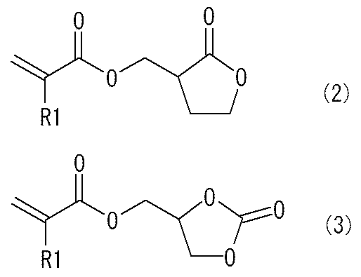
- 環状エステル残基又は環状アミド残基を有する(メタ)アクリレートが、以下式(1)
(式中、R1は水素原子又はメチル基であり、R2はアルキレン基又はアルキルオキシ基であり、R3はアルキル基、アルキレン基、アリール基又はハロゲン原子であり、nは0〜3の整数であり、R4は存在しないか又は酸素原子で置換してもよいアルキレン基であり、R4が存在しない場合、R4の両側の実線はそれらで単結合を表し、X1は存在しないか又は酸素原子もしくは炭素原子であり、X1が存在しない場合、X1の両側の実線はそれらで単結合を表し、X2は酸素原子、窒素原子又は硫黄原子である。)
の構造式で表される請求項1記載の異方性導電フィルム。 - 環状エステル残基を有する(メタ)アクリレートが、以下式(2)又は(3)
- (メタ)アクリレート系モノマー組成物とラジカル重合開始剤と成膜用樹脂とを含有する絶縁性接着剤組成物に導電粒子を均一に分散混合し、得られた混合物を剥離フィルムに塗布し、乾燥することにより異方性導電フィルムを製造する方法において、(メタ)アクリレート系モノマー組成物が環状エステル残基又は環状アミド残基を有する(メタ)アクリレート系モノマーを含有する製造方法。
- 環状エステル残基又は環状アミド残基を有する(メタ)アクリレートが、以下式(1)
(式中、R1は水素原子又はメチル基であり、R2はアルキレン基又はアルキルオキシ基であり、R3はアルキル基、アルキレン基、アリール基又はハロゲン原子であり、nは0〜3の整数であり、R4は存在しないか又は酸素原子で置換してもよいアルキレン基であり、R4が存在しない場合、R4の両側の実線はそれらで単結合を表し、X1は存在しないか又は酸素原子もしくは炭素原子であり、X1が存在しない場合、X1の両側の実線はそれらで単結合を表し、X2は酸素原子、窒素原子又は硫黄原子である。)
の構造式で表される請求項4記載の製造方法。 - 環状エステル残基を有する(メタ)アクリレートが、以下式(2)又は(3)
- 第1の電子部品の端子と第2の電子部品の端子とが、請求項1〜3のいずれかに記載の異方性導電フィルムを介して異方性導電接続されてなる接続構造体。
- 第1の電子部品の端子と第2の電子部品の端子とが、異方性導電フィルムを介して異方性導電接続されてなる接続構造体の製造方法において、
第1の電子部品の端子上に請求項1〜3のいずれかに記載の異方性導電フィルムを仮貼りし、
仮貼りされた異方性導電フィルム上に第2の電子部品を、第1の電子部品の端子と第2の電子部品の端子とが対向するように仮設置し、
仮設置された第2の電子部品を加熱加圧することにより、第1の電子部品の端子と第2の電子部品の端子とを異方性導電接続する製造方法。
Priority Applications (6)
| Application Number | Priority Date | Filing Date | Title |
|---|---|---|---|
| JP2010164134A JP5521848B2 (ja) | 2010-07-21 | 2010-07-21 | 異方性導電フィルム、接続構造体及びそれらの製造方法 |
| PCT/JP2011/066309 WO2012011457A1 (ja) | 2010-07-21 | 2011-07-19 | 異方性導電フィルム、接続構造体及びそれらの製造方法 |
| US13/512,752 US9515042B2 (en) | 2010-07-21 | 2011-07-19 | Anisotropic conductive film, connection structure and method of producing the same |
| CN201180035632.6A CN103081235B (zh) | 2010-07-21 | 2011-07-19 | 各向异性导电膜、连接结构体以及它们的制作方法 |
| KR1020127018903A KR101312748B1 (ko) | 2010-07-21 | 2011-07-19 | 이방성 도전 필름, 접속 구조체 및 그들의 제조 방법 |
| HK13108692.9A HK1181557A1 (zh) | 2010-07-21 | 2013-07-24 | 各向異性導電膜、連接結構體以及它們的製作方法 |
Applications Claiming Priority (1)
| Application Number | Priority Date | Filing Date | Title |
|---|---|---|---|
| JP2010164134A JP5521848B2 (ja) | 2010-07-21 | 2010-07-21 | 異方性導電フィルム、接続構造体及びそれらの製造方法 |
Publications (2)
| Publication Number | Publication Date |
|---|---|
| JP2010242101A JP2010242101A (ja) | 2010-10-28 |
| JP5521848B2 true JP5521848B2 (ja) | 2014-06-18 |
Family
ID=43095445
Family Applications (1)
| Application Number | Title | Priority Date | Filing Date |
|---|---|---|---|
| JP2010164134A Active JP5521848B2 (ja) | 2010-07-21 | 2010-07-21 | 異方性導電フィルム、接続構造体及びそれらの製造方法 |
Country Status (6)
| Country | Link |
|---|---|
| US (1) | US9515042B2 (ja) |
| JP (1) | JP5521848B2 (ja) |
| KR (1) | KR101312748B1 (ja) |
| CN (1) | CN103081235B (ja) |
| HK (1) | HK1181557A1 (ja) |
| WO (1) | WO2012011457A1 (ja) |
Families Citing this family (10)
| Publication number | Priority date | Publication date | Assignee | Title |
|---|---|---|---|---|
| KR101583691B1 (ko) * | 2012-10-10 | 2016-01-08 | 제일모직주식회사 | 이방 전도성 접착 조성물 및 이를 이용한 이방 전도성 필름 |
| US20150353756A1 (en) | 2012-12-27 | 2015-12-10 | 3M Innovative Properties Company | Coatings for indium-tin oxide layers |
| JP2015025028A (ja) * | 2013-07-24 | 2015-02-05 | 日立化成株式会社 | 接続材料、これを用いた接続構造体及びその製造方法 |
| JP6127806B2 (ja) * | 2013-07-24 | 2017-05-17 | 日立化成株式会社 | 接続材料、接続構造体及びその製造方法 |
| WO2016143640A1 (ja) * | 2015-03-11 | 2016-09-15 | セメダイン株式会社 | 導電性構造体、及び導電性構造体の製造方法 |
| KR20180057681A (ko) * | 2015-09-21 | 2018-05-30 | 로오드 코포레이션 | 접착제 조성물 및 접합 방법 |
| US11279861B2 (en) * | 2017-02-20 | 2022-03-22 | Lord Corporation | Adhesive compositions based on grafted resins |
| JP7284703B2 (ja) * | 2018-04-04 | 2023-05-31 | 積水化学工業株式会社 | 絶縁性粒子付き導電性粒子、導電材料及び接続構造体 |
| JP7434306B2 (ja) | 2019-05-20 | 2024-02-20 | リンテック株式会社 | 粘着剤組成物および粘着シート |
| JPWO2021225038A1 (ja) * | 2020-05-07 | 2021-11-11 |
Family Cites Families (23)
| Publication number | Priority date | Publication date | Assignee | Title |
|---|---|---|---|---|
| US5639546A (en) * | 1991-09-03 | 1997-06-17 | Minnesota Mining And Manufacturing Company | Coated article having improved adhesion to organic coatings |
| KR100832282B1 (ko) * | 2000-10-23 | 2008-05-26 | 세키스이가가쿠 고교가부시키가이샤 | 피복 입자 |
| JP3803286B2 (ja) * | 2001-12-03 | 2006-08-02 | 東京応化工業株式会社 | ポジ型レジスト組成物及びレジストパターンの形成方法 |
| JP2003313533A (ja) | 2002-04-23 | 2003-11-06 | Sumitomo Bakelite Co Ltd | 異方導電性接着剤 |
| DE10259451A1 (de) * | 2002-12-19 | 2004-07-08 | Tesa Ag | Haftklebeartikel mit wenigstens einer Schicht aus einer thermisch leitfähigen Haftklebemasse und Verfahren zu seiner Herstellung |
| JP3921459B2 (ja) | 2003-07-11 | 2007-05-30 | ソニーケミカル&インフォメーションデバイス株式会社 | 電気部品の実装方法及び実装装置 |
| JP2005036081A (ja) * | 2003-07-18 | 2005-02-10 | Mitsubishi Chemicals Corp | 5員環カーボネート基を有する(メタ)アクリル酸系共重合体及びそれを含有する硬化性樹脂組成物 |
| US7045586B2 (en) * | 2003-08-14 | 2006-05-16 | Dow Corning Corporation | Adhesives having improved chemical resistance and curable silicone compositions for preparing the adhesives |
| DE102004002279A1 (de) * | 2004-01-16 | 2005-08-04 | Tesa Ag | Orientierte Acrylathaftklebemassen, Verfahren zu ihrer Herstellung und ihre Verwendung |
| JP4741286B2 (ja) | 2004-06-11 | 2011-08-03 | 株式会社半導体エネルギー研究所 | 半導体装置及びその作製方法 |
| KR100601341B1 (ko) * | 2004-06-23 | 2006-07-14 | 엘에스전선 주식회사 | 이방 도전성 접착제 및 이를 이용한 접착필름 |
| JP4878778B2 (ja) | 2005-06-01 | 2012-02-15 | 富士フイルム株式会社 | 導電性ハードコートフィルム、反射防止フィルム、偏光板、及び画像表示装置 |
| JP4631689B2 (ja) * | 2005-12-14 | 2011-02-16 | ダイキン工業株式会社 | イオン伝導体 |
| KR101440653B1 (ko) * | 2007-02-15 | 2014-09-19 | 바스프 에스이 | N-히드록시알킬화 락탐의 (메트)아크릴산 에스테르의 제조 방법 |
| JP5181220B2 (ja) | 2007-04-19 | 2013-04-10 | 日立化成株式会社 | 回路接続用接着フィルム、接続構造体及びその製造方法 |
| JP2009057518A (ja) * | 2007-09-03 | 2009-03-19 | Institute Of Physical & Chemical Research | 異方性フィルムおよび異方性フィルムの製造方法 |
| JP5131109B2 (ja) * | 2007-09-20 | 2013-01-30 | 東レ株式会社 | 電子部品用接着剤組成物およびそれを用いた電子部品用接着剤シート |
| US20090142593A1 (en) * | 2007-11-29 | 2009-06-04 | Nitto Denko Corporation | Pressure-sensitive adhesive tape |
| TWI389999B (zh) | 2007-12-18 | 2013-03-21 | Cheil Ind Inc | 黏著性組成物及使用該黏著性組成物的各向異性導電膜 |
| EP2307516B1 (en) * | 2008-07-28 | 2012-09-05 | Dow Corning Corporation | Composite article |
| WO2010038574A1 (ja) * | 2008-09-30 | 2010-04-08 | ソニーケミカル&インフォメーションデバイス株式会社 | アクリル系絶縁性接着剤 |
| JP2010111847A (ja) | 2008-10-09 | 2010-05-20 | Hitachi Chem Co Ltd | 接着剤組成物及び接続体 |
| WO2012101245A1 (en) * | 2011-01-28 | 2012-08-02 | Basf Se | Polymerizable composition comprising an oxime sulfonate as thermal curing agent |
-
2010
- 2010-07-21 JP JP2010164134A patent/JP5521848B2/ja active Active
-
2011
- 2011-07-19 CN CN201180035632.6A patent/CN103081235B/zh active Active
- 2011-07-19 KR KR1020127018903A patent/KR101312748B1/ko active IP Right Grant
- 2011-07-19 US US13/512,752 patent/US9515042B2/en active Active
- 2011-07-19 WO PCT/JP2011/066309 patent/WO2012011457A1/ja active Application Filing
-
2013
- 2013-07-24 HK HK13108692.9A patent/HK1181557A1/zh unknown
Also Published As
| Publication number | Publication date |
|---|---|
| KR20120106985A (ko) | 2012-09-27 |
| CN103081235A (zh) | 2013-05-01 |
| CN103081235B (zh) | 2016-06-01 |
| US20120228026A1 (en) | 2012-09-13 |
| WO2012011457A1 (ja) | 2012-01-26 |
| KR101312748B1 (ko) | 2013-09-27 |
| JP2010242101A (ja) | 2010-10-28 |
| HK1181557A1 (zh) | 2013-11-08 |
| US9515042B2 (en) | 2016-12-06 |
Similar Documents
| Publication | Publication Date | Title |
|---|---|---|
| JP5521848B2 (ja) | 異方性導電フィルム、接続構造体及びそれらの製造方法 | |
| KR101615797B1 (ko) | 이방성 도전 필름 | |
| KR101296486B1 (ko) | 접착제 조성물, 접속 구조체, 접속 구조체의 제조 방법 및 접착제 조성물의 용도 | |
| JP4590732B2 (ja) | 回路接続材料及びそれを用いた回路板の製造方法、回路板 | |
| EP1229095A1 (en) | Adhesive agent, method for connecting wiring terminals and wiring structure | |
| JP6065407B2 (ja) | 回路接続材料、フィルム状回路接続材料、回路接続シート、回路接続体及び回路部材の接続方法 | |
| JP6532850B2 (ja) | 接着剤組成物、フィルム状接着剤、接着シート、回路接続体、回路部材の接続方法、接着剤組成物の使用、フィルム状接着剤の使用及び接着シートの使用 | |
| JP5844588B2 (ja) | 回路接続材料及びそれを用いた接続方法並びに接続構造体 | |
| JP2013101942A (ja) | 回路接続用接着フィルム、これを用いた回路接続構造体及び回路部材の接続方法 | |
| KR101899594B1 (ko) | 대향 전극 접속용 접착제 | |
| JP5577635B2 (ja) | 接着剤組成物、回路接続用接着剤及び回路接続体 | |
| TW202402994A (zh) | 電路連接用接著劑組成物及結構體 | |
| CN103797078B (zh) | 电路连接材料以及使用该电路连接材料的连接方法和连接结构体 | |
| KR101955749B1 (ko) | 이방 도전성 필름용 조성물, 이방 도전성 필름 및 이를 이용한 반도체 장치 | |
| JP4831086B2 (ja) | ゴム変性フェノキシ樹脂及びこれを用いた樹脂組成物、回路部材接続用接着剤並びに回路接続構造体 | |
| JP4635312B2 (ja) | 接着剤組成物、回路接続材料、回路接続用接着剤組成物、接続体及び半導体装置 | |
| JP2010212706A (ja) | 回路接続材料及びそれを用いた回路板の製造方法、回路板 | |
| JP2010111847A (ja) | 接着剤組成物及び接続体 | |
| JP2012021141A (ja) | 回路接続用接着フィルム、これを用いた回路接続構造体及び回路部材の接続方法 | |
| JP2006012804A (ja) | 接着剤、配線端子の接続方法及び配線構造体 |
Legal Events
| Date | Code | Title | Description |
|---|---|---|---|
| A621 | Written request for application examination |
Free format text: JAPANESE INTERMEDIATE CODE: A621 Effective date: 20130307 |
|
| TRDD | Decision of grant or rejection written | ||
| A01 | Written decision to grant a patent or to grant a registration (utility model) |
Free format text: JAPANESE INTERMEDIATE CODE: A01 Effective date: 20140311 |
|
| A61 | First payment of annual fees (during grant procedure) |
Free format text: JAPANESE INTERMEDIATE CODE: A61 Effective date: 20140324 |
|
| R150 | Certificate of patent or registration of utility model |
Ref document number: 5521848 Country of ref document: JP Free format text: JAPANESE INTERMEDIATE CODE: R150 |
|
| R250 | Receipt of annual fees |
Free format text: JAPANESE INTERMEDIATE CODE: R250 |
|
| R250 | Receipt of annual fees |
Free format text: JAPANESE INTERMEDIATE CODE: R250 |
|
| R250 | Receipt of annual fees |
Free format text: JAPANESE INTERMEDIATE CODE: R250 |
|
| R250 | Receipt of annual fees |
Free format text: JAPANESE INTERMEDIATE CODE: R250 |
|
| R250 | Receipt of annual fees |
Free format text: JAPANESE INTERMEDIATE CODE: R250 |
|
| R250 | Receipt of annual fees |
Free format text: JAPANESE INTERMEDIATE CODE: R250 |
|
| R250 | Receipt of annual fees |
Free format text: JAPANESE INTERMEDIATE CODE: R250 |
|
| S531 | Written request for registration of change of domicile |
Free format text: JAPANESE INTERMEDIATE CODE: R313531 |
|
| R350 | Written notification of registration of transfer |
Free format text: JAPANESE INTERMEDIATE CODE: R350 |
|
| R154 | Certificate of patent or utility model (reissue) |
Free format text: JAPANESE INTERMEDIATE CODE: R154 |
|
| R250 | Receipt of annual fees |
Free format text: JAPANESE INTERMEDIATE CODE: R250 |