JP5518381B2 - カラーセンサ及び当該カラーセンサを具備する電子機器 - Google Patents
カラーセンサ及び当該カラーセンサを具備する電子機器 Download PDFInfo
- Publication number
- JP5518381B2 JP5518381B2 JP2009158854A JP2009158854A JP5518381B2 JP 5518381 B2 JP5518381 B2 JP 5518381B2 JP 2009158854 A JP2009158854 A JP 2009158854A JP 2009158854 A JP2009158854 A JP 2009158854A JP 5518381 B2 JP5518381 B2 JP 5518381B2
- Authority
- JP
- Japan
- Prior art keywords
- light
- layer
- conversion circuit
- optical filter
- wiring
- Prior art date
- Legal status (The legal status is an assumption and is not a legal conclusion. Google has not performed a legal analysis and makes no representation as to the accuracy of the status listed.)
- Expired - Fee Related
Links
- 230000003287 optical effect Effects 0.000 claims description 433
- 238000006243 chemical reaction Methods 0.000 claims description 190
- 229920005989 resin Polymers 0.000 claims description 103
- 239000011347 resin Substances 0.000 claims description 103
- 239000010410 layer Substances 0.000 description 374
- 239000000758 substrate Substances 0.000 description 322
- 239000004065 semiconductor Substances 0.000 description 317
- 239000010408 film Substances 0.000 description 282
- 239000013078 crystal Substances 0.000 description 190
- 238000000034 method Methods 0.000 description 104
- 150000002500 ions Chemical class 0.000 description 66
- 239000007789 gas Substances 0.000 description 43
- 238000010438 heat treatment Methods 0.000 description 42
- 239000001257 hydrogen Substances 0.000 description 42
- 229910052739 hydrogen Inorganic materials 0.000 description 42
- VYPSYNLAJGMNEJ-UHFFFAOYSA-N Silicium dioxide Chemical compound O=[Si]=O VYPSYNLAJGMNEJ-UHFFFAOYSA-N 0.000 description 36
- 229910052814 silicon oxide Inorganic materials 0.000 description 36
- UFHFLCQGNIYNRP-UHFFFAOYSA-N Hydrogen Chemical compound [H][H] UFHFLCQGNIYNRP-UHFFFAOYSA-N 0.000 description 32
- IJGRMHOSHXDMSA-UHFFFAOYSA-N Atomic nitrogen Chemical compound N#N IJGRMHOSHXDMSA-UHFFFAOYSA-N 0.000 description 30
- 239000000463 material Substances 0.000 description 28
- 229910052710 silicon Inorganic materials 0.000 description 27
- XUIMIQQOPSSXEZ-UHFFFAOYSA-N Silicon Chemical compound [Si] XUIMIQQOPSSXEZ-UHFFFAOYSA-N 0.000 description 26
- 239000012535 impurity Substances 0.000 description 26
- 229910052751 metal Inorganic materials 0.000 description 26
- 239000002184 metal Substances 0.000 description 26
- 230000008569 process Effects 0.000 description 26
- 230000006870 function Effects 0.000 description 25
- 239000010703 silicon Substances 0.000 description 25
- XKRFYHLGVUSROY-UHFFFAOYSA-N Argon Chemical compound [Ar] XKRFYHLGVUSROY-UHFFFAOYSA-N 0.000 description 24
- 230000007547 defect Effects 0.000 description 24
- PXHVJJICTQNCMI-UHFFFAOYSA-N Nickel Chemical compound [Ni] PXHVJJICTQNCMI-UHFFFAOYSA-N 0.000 description 23
- 229910052581 Si3N4 Inorganic materials 0.000 description 23
- 239000011229 interlayer Substances 0.000 description 23
- 239000001301 oxygen Substances 0.000 description 23
- 229910052760 oxygen Inorganic materials 0.000 description 23
- HQVNEWCFYHHQES-UHFFFAOYSA-N silicon nitride Chemical compound N12[Si]34N5[Si]62N3[Si]51N64 HQVNEWCFYHHQES-UHFFFAOYSA-N 0.000 description 23
- 239000011241 protective layer Substances 0.000 description 22
- QVGXLLKOCUKJST-UHFFFAOYSA-N atomic oxygen Chemical compound [O] QVGXLLKOCUKJST-UHFFFAOYSA-N 0.000 description 21
- 238000002425 crystallisation Methods 0.000 description 20
- -1 silver halide Chemical class 0.000 description 20
- 229910052736 halogen Inorganic materials 0.000 description 19
- 230000001681 protective effect Effects 0.000 description 19
- 239000012298 atmosphere Substances 0.000 description 18
- 238000004519 manufacturing process Methods 0.000 description 18
- 238000004544 sputter deposition Methods 0.000 description 18
- 239000010936 titanium Substances 0.000 description 18
- 238000005229 chemical vapour deposition Methods 0.000 description 17
- 230000008025 crystallization Effects 0.000 description 17
- 150000002367 halogens Chemical class 0.000 description 17
- KRHYYFGTRYWZRS-UHFFFAOYSA-N Fluorane Chemical compound F KRHYYFGTRYWZRS-UHFFFAOYSA-N 0.000 description 16
- 238000005520 cutting process Methods 0.000 description 16
- 238000005247 gettering Methods 0.000 description 16
- 235000012431 wafers Nutrition 0.000 description 16
- BLRPTPMANUNPDV-UHFFFAOYSA-N Silane Chemical compound [SiH4] BLRPTPMANUNPDV-UHFFFAOYSA-N 0.000 description 15
- 229910021417 amorphous silicon Inorganic materials 0.000 description 14
- 229910052757 nitrogen Inorganic materials 0.000 description 14
- 238000005268 plasma chemical vapour deposition Methods 0.000 description 14
- 238000012937 correction Methods 0.000 description 13
- 229910021421 monocrystalline silicon Inorganic materials 0.000 description 13
- 238000005498 polishing Methods 0.000 description 13
- 229910021420 polycrystalline silicon Inorganic materials 0.000 description 13
- KDLHZDBZIXYQEI-UHFFFAOYSA-N Palladium Chemical compound [Pd] KDLHZDBZIXYQEI-UHFFFAOYSA-N 0.000 description 12
- 229910052786 argon Inorganic materials 0.000 description 12
- 230000004888 barrier function Effects 0.000 description 12
- BASFCYQUMIYNBI-UHFFFAOYSA-N platinum Chemical compound [Pt] BASFCYQUMIYNBI-UHFFFAOYSA-N 0.000 description 12
- 230000035939 shock Effects 0.000 description 12
- 239000000126 substance Substances 0.000 description 12
- XLOMVQKBTHCTTD-UHFFFAOYSA-N Zinc monoxide Chemical compound [Zn]=O XLOMVQKBTHCTTD-UHFFFAOYSA-N 0.000 description 11
- 230000015572 biosynthetic process Effects 0.000 description 11
- 230000003647 oxidation Effects 0.000 description 11
- 238000007254 oxidation reaction Methods 0.000 description 11
- 229910052782 aluminium Inorganic materials 0.000 description 10
- XAGFODPZIPBFFR-UHFFFAOYSA-N aluminium Chemical compound [Al] XAGFODPZIPBFFR-UHFFFAOYSA-N 0.000 description 10
- 230000000694 effects Effects 0.000 description 10
- 229910000077 silane Inorganic materials 0.000 description 10
- 230000000903 blocking effect Effects 0.000 description 9
- 238000004140 cleaning Methods 0.000 description 9
- 239000010931 gold Substances 0.000 description 9
- 238000005468 ion implantation Methods 0.000 description 9
- 239000004973 liquid crystal related substance Substances 0.000 description 9
- 229910021424 microcrystalline silicon Inorganic materials 0.000 description 9
- 229910052759 nickel Inorganic materials 0.000 description 9
- 238000012545 processing Methods 0.000 description 9
- 238000007789 sealing Methods 0.000 description 9
- MHAJPDPJQMAIIY-UHFFFAOYSA-N Hydrogen peroxide Chemical compound OO MHAJPDPJQMAIIY-UHFFFAOYSA-N 0.000 description 8
- 230000001133 acceleration Effects 0.000 description 8
- 239000002585 base Substances 0.000 description 8
- 230000005540 biological transmission Effects 0.000 description 8
- 230000006835 compression Effects 0.000 description 8
- 238000007906 compression Methods 0.000 description 8
- 230000005669 field effect Effects 0.000 description 8
- 229910052731 fluorine Inorganic materials 0.000 description 8
- 239000011737 fluorine Substances 0.000 description 8
- 239000011521 glass Substances 0.000 description 8
- 239000001307 helium Substances 0.000 description 8
- 229910052734 helium Inorganic materials 0.000 description 8
- SWQJXJOGLNCZEY-UHFFFAOYSA-N helium atom Chemical compound [He] SWQJXJOGLNCZEY-UHFFFAOYSA-N 0.000 description 8
- 230000001678 irradiating effect Effects 0.000 description 8
- 239000002245 particle Substances 0.000 description 8
- 239000002356 single layer Substances 0.000 description 8
- 241000894007 species Species 0.000 description 8
- 229910052719 titanium Inorganic materials 0.000 description 8
- XLYOFNOQVPJJNP-UHFFFAOYSA-N water Chemical compound O XLYOFNOQVPJJNP-UHFFFAOYSA-N 0.000 description 8
- VEXZGXHMUGYJMC-UHFFFAOYSA-N Hydrochloric acid Chemical compound Cl VEXZGXHMUGYJMC-UHFFFAOYSA-N 0.000 description 7
- RTAQQCXQSZGOHL-UHFFFAOYSA-N Titanium Chemical compound [Ti] RTAQQCXQSZGOHL-UHFFFAOYSA-N 0.000 description 7
- 239000000460 chlorine Substances 0.000 description 7
- 238000000576 coating method Methods 0.000 description 7
- 150000001875 compounds Chemical class 0.000 description 7
- 230000002950 deficient Effects 0.000 description 7
- 239000011261 inert gas Substances 0.000 description 7
- TWNQGVIAIRXVLR-UHFFFAOYSA-N oxo(oxoalumanyloxy)alumane Chemical compound O=[Al]O[Al]=O TWNQGVIAIRXVLR-UHFFFAOYSA-N 0.000 description 7
- 229920005591 polysilicon Polymers 0.000 description 7
- 229910000679 solder Inorganic materials 0.000 description 7
- GQPLMRYTRLFLPF-UHFFFAOYSA-N Nitrous Oxide Chemical compound [O-][N+]#N GQPLMRYTRLFLPF-UHFFFAOYSA-N 0.000 description 6
- 239000003086 colorant Substances 0.000 description 6
- 239000010949 copper Substances 0.000 description 6
- 229910052732 germanium Inorganic materials 0.000 description 6
- GNPVGFCGXDBREM-UHFFFAOYSA-N germanium atom Chemical compound [Ge] GNPVGFCGXDBREM-UHFFFAOYSA-N 0.000 description 6
- 238000007689 inspection Methods 0.000 description 6
- 239000011777 magnesium Substances 0.000 description 6
- 230000007257 malfunction Effects 0.000 description 6
- 150000001282 organosilanes Chemical class 0.000 description 6
- 230000010355 oscillation Effects 0.000 description 6
- 230000001590 oxidative effect Effects 0.000 description 6
- 238000009832 plasma treatment Methods 0.000 description 6
- 239000000047 product Substances 0.000 description 6
- 239000010948 rhodium Substances 0.000 description 6
- 238000000926 separation method Methods 0.000 description 6
- 239000010409 thin film Substances 0.000 description 6
- YCKRFDGAMUMZLT-UHFFFAOYSA-N Fluorine atom Chemical compound [F] YCKRFDGAMUMZLT-UHFFFAOYSA-N 0.000 description 5
- FYYHWMGAXLPEAU-UHFFFAOYSA-N Magnesium Chemical compound [Mg] FYYHWMGAXLPEAU-UHFFFAOYSA-N 0.000 description 5
- CBENFWSGALASAD-UHFFFAOYSA-N Ozone Chemical compound [O-][O+]=O CBENFWSGALASAD-UHFFFAOYSA-N 0.000 description 5
- 239000000956 alloy Substances 0.000 description 5
- 238000000151 deposition Methods 0.000 description 5
- KPUWHANPEXNPJT-UHFFFAOYSA-N disiloxane Chemical class [SiH3]O[SiH3] KPUWHANPEXNPJT-UHFFFAOYSA-N 0.000 description 5
- 238000005530 etching Methods 0.000 description 5
- 229910052737 gold Inorganic materials 0.000 description 5
- 229910052749 magnesium Inorganic materials 0.000 description 5
- 230000000149 penetrating effect Effects 0.000 description 5
- 239000002994 raw material Substances 0.000 description 5
- 229910052721 tungsten Inorganic materials 0.000 description 5
- 239000010937 tungsten Substances 0.000 description 5
- 230000003313 weakening effect Effects 0.000 description 5
- JBRZTFJDHDCESZ-UHFFFAOYSA-N AsGa Chemical compound [As]#[Ga] JBRZTFJDHDCESZ-UHFFFAOYSA-N 0.000 description 4
- ZOXJGFHDIHLPTG-UHFFFAOYSA-N Boron Chemical compound [B] ZOXJGFHDIHLPTG-UHFFFAOYSA-N 0.000 description 4
- OKTJSMMVPCPJKN-UHFFFAOYSA-N Carbon Chemical compound [C] OKTJSMMVPCPJKN-UHFFFAOYSA-N 0.000 description 4
- ZAMOUSCENKQFHK-UHFFFAOYSA-N Chlorine atom Chemical compound [Cl] ZAMOUSCENKQFHK-UHFFFAOYSA-N 0.000 description 4
- 229910001218 Gallium arsenide Inorganic materials 0.000 description 4
- ZOKXTWBITQBERF-UHFFFAOYSA-N Molybdenum Chemical compound [Mo] ZOKXTWBITQBERF-UHFFFAOYSA-N 0.000 description 4
- OAICVXFJPJFONN-UHFFFAOYSA-N Phosphorus Chemical compound [P] OAICVXFJPJFONN-UHFFFAOYSA-N 0.000 description 4
- GWEVSGVZZGPLCZ-UHFFFAOYSA-N Titan oxide Chemical compound O=[Ti]=O GWEVSGVZZGPLCZ-UHFFFAOYSA-N 0.000 description 4
- 230000009471 action Effects 0.000 description 4
- 125000004429 atom Chemical group 0.000 description 4
- 229910052796 boron Inorganic materials 0.000 description 4
- 230000003197 catalytic effect Effects 0.000 description 4
- 230000008859 change Effects 0.000 description 4
- 229910052801 chlorine Inorganic materials 0.000 description 4
- 238000010586 diagram Methods 0.000 description 4
- 238000009792 diffusion process Methods 0.000 description 4
- PCHJSUWPFVWCPO-UHFFFAOYSA-N gold Chemical compound [Au] PCHJSUWPFVWCPO-UHFFFAOYSA-N 0.000 description 4
- 238000000227 grinding Methods 0.000 description 4
- IXCSERBJSXMMFS-UHFFFAOYSA-N hydrogen chloride Substances Cl.Cl IXCSERBJSXMMFS-UHFFFAOYSA-N 0.000 description 4
- 229910000041 hydrogen chloride Inorganic materials 0.000 description 4
- 229910052750 molybdenum Inorganic materials 0.000 description 4
- 239000011733 molybdenum Substances 0.000 description 4
- 239000012299 nitrogen atmosphere Substances 0.000 description 4
- 229910052763 palladium Inorganic materials 0.000 description 4
- 239000012071 phase Substances 0.000 description 4
- 229910052698 phosphorus Inorganic materials 0.000 description 4
- 239000011574 phosphorus Substances 0.000 description 4
- 229910052697 platinum Inorganic materials 0.000 description 4
- 238000007639 printing Methods 0.000 description 4
- 238000004151 rapid thermal annealing Methods 0.000 description 4
- 229910052712 strontium Inorganic materials 0.000 description 4
- CIOAGBVUUVVLOB-UHFFFAOYSA-N strontium atom Chemical compound [Sr] CIOAGBVUUVVLOB-UHFFFAOYSA-N 0.000 description 4
- IATRAKWUXMZMIY-UHFFFAOYSA-N strontium oxide Chemical compound [O-2].[Sr+2] IATRAKWUXMZMIY-UHFFFAOYSA-N 0.000 description 4
- 229910052715 tantalum Inorganic materials 0.000 description 4
- GUVRBAGPIYLISA-UHFFFAOYSA-N tantalum atom Chemical compound [Ta] GUVRBAGPIYLISA-UHFFFAOYSA-N 0.000 description 4
- WGTYBPLFGIVFAS-UHFFFAOYSA-M tetramethylammonium hydroxide Chemical compound [OH-].C[N+](C)(C)C WGTYBPLFGIVFAS-UHFFFAOYSA-M 0.000 description 4
- 239000011787 zinc oxide Substances 0.000 description 4
- RYGMFSIKBFXOCR-UHFFFAOYSA-N Copper Chemical compound [Cu] RYGMFSIKBFXOCR-UHFFFAOYSA-N 0.000 description 3
- GPXJNWSHGFTCBW-UHFFFAOYSA-N Indium phosphide Chemical compound [In]#P GPXJNWSHGFTCBW-UHFFFAOYSA-N 0.000 description 3
- KJTLSVCANCCWHF-UHFFFAOYSA-N Ruthenium Chemical compound [Ru] KJTLSVCANCCWHF-UHFFFAOYSA-N 0.000 description 3
- 238000005411 Van der Waals force Methods 0.000 description 3
- 229910045601 alloy Inorganic materials 0.000 description 3
- 238000000137 annealing Methods 0.000 description 3
- 238000013459 approach Methods 0.000 description 3
- 238000004364 calculation method Methods 0.000 description 3
- 229910052799 carbon Inorganic materials 0.000 description 3
- 239000003054 catalyst Substances 0.000 description 3
- 150000001805 chlorine compounds Chemical class 0.000 description 3
- 238000003776 cleavage reaction Methods 0.000 description 3
- 229910017052 cobalt Inorganic materials 0.000 description 3
- 239000010941 cobalt Substances 0.000 description 3
- GUTLYIVDDKVIGB-UHFFFAOYSA-N cobalt atom Chemical compound [Co] GUTLYIVDDKVIGB-UHFFFAOYSA-N 0.000 description 3
- 229910052802 copper Inorganic materials 0.000 description 3
- 230000008021 deposition Effects 0.000 description 3
- 239000000428 dust Substances 0.000 description 3
- 238000001678 elastic recoil detection analysis Methods 0.000 description 3
- 150000002431 hydrogen Chemical class 0.000 description 3
- AMGQUBHHOARCQH-UHFFFAOYSA-N indium;oxotin Chemical compound [In].[Sn]=O AMGQUBHHOARCQH-UHFFFAOYSA-N 0.000 description 3
- 239000011810 insulating material Substances 0.000 description 3
- 230000010354 integration Effects 0.000 description 3
- 238000010884 ion-beam technique Methods 0.000 description 3
- 229910052741 iridium Inorganic materials 0.000 description 3
- GKOZUEZYRPOHIO-UHFFFAOYSA-N iridium atom Chemical compound [Ir] GKOZUEZYRPOHIO-UHFFFAOYSA-N 0.000 description 3
- 229910052743 krypton Inorganic materials 0.000 description 3
- DNNSSWSSYDEUBZ-UHFFFAOYSA-N krypton atom Chemical compound [Kr] DNNSSWSSYDEUBZ-UHFFFAOYSA-N 0.000 description 3
- 229910044991 metal oxide Inorganic materials 0.000 description 3
- 150000004706 metal oxides Chemical class 0.000 description 3
- 150000002739 metals Chemical class 0.000 description 3
- 239000013081 microcrystal Substances 0.000 description 3
- 229910052754 neon Inorganic materials 0.000 description 3
- GKAOGPIIYCISHV-UHFFFAOYSA-N neon atom Chemical compound [Ne] GKAOGPIIYCISHV-UHFFFAOYSA-N 0.000 description 3
- 150000004767 nitrides Chemical class 0.000 description 3
- 239000001272 nitrous oxide Substances 0.000 description 3
- 229910052762 osmium Inorganic materials 0.000 description 3
- SYQBFIAQOQZEGI-UHFFFAOYSA-N osmium atom Chemical compound [Os] SYQBFIAQOQZEGI-UHFFFAOYSA-N 0.000 description 3
- 238000007517 polishing process Methods 0.000 description 3
- 150000003254 radicals Chemical class 0.000 description 3
- 229910052703 rhodium Inorganic materials 0.000 description 3
- MHOVAHRLVXNVSD-UHFFFAOYSA-N rhodium atom Chemical compound [Rh] MHOVAHRLVXNVSD-UHFFFAOYSA-N 0.000 description 3
- 229910052707 ruthenium Inorganic materials 0.000 description 3
- 238000005001 rutherford backscattering spectroscopy Methods 0.000 description 3
- 230000007017 scission Effects 0.000 description 3
- 229910052990 silicon hydride Inorganic materials 0.000 description 3
- 229910052709 silver Inorganic materials 0.000 description 3
- 239000004332 silver Substances 0.000 description 3
- 239000000243 solution Substances 0.000 description 3
- 230000035882 stress Effects 0.000 description 3
- 125000001424 substituent group Chemical group 0.000 description 3
- 238000012546 transfer Methods 0.000 description 3
- WFKWXMTUELFFGS-UHFFFAOYSA-N tungsten Chemical compound [W] WFKWXMTUELFFGS-UHFFFAOYSA-N 0.000 description 3
- 238000007740 vapor deposition Methods 0.000 description 3
- 238000001039 wet etching Methods 0.000 description 3
- 229910052724 xenon Inorganic materials 0.000 description 3
- FHNFHKCVQCLJFQ-UHFFFAOYSA-N xenon atom Chemical compound [Xe] FHNFHKCVQCLJFQ-UHFFFAOYSA-N 0.000 description 3
- WZJUBBHODHNQPW-UHFFFAOYSA-N 2,4,6,8-tetramethyl-1,3,5,7,2$l^{3},4$l^{3},6$l^{3},8$l^{3}-tetraoxatetrasilocane Chemical compound C[Si]1O[Si](C)O[Si](C)O[Si](C)O1 WZJUBBHODHNQPW-UHFFFAOYSA-N 0.000 description 2
- QGZKDVFQNNGYKY-UHFFFAOYSA-N Ammonia Chemical compound N QGZKDVFQNNGYKY-UHFFFAOYSA-N 0.000 description 2
- 229910052779 Neodymium Inorganic materials 0.000 description 2
- 238000001237 Raman spectrum Methods 0.000 description 2
- BQCADISMDOOEFD-UHFFFAOYSA-N Silver Chemical compound [Ag] BQCADISMDOOEFD-UHFFFAOYSA-N 0.000 description 2
- 229910006404 SnO 2 Inorganic materials 0.000 description 2
- QAOWNCQODCNURD-UHFFFAOYSA-N Sulfuric acid Chemical compound OS(O)(=O)=O QAOWNCQODCNURD-UHFFFAOYSA-N 0.000 description 2
- BOTDANWDWHJENH-UHFFFAOYSA-N Tetraethyl orthosilicate Chemical compound CCO[Si](OCC)(OCC)OCC BOTDANWDWHJENH-UHFFFAOYSA-N 0.000 description 2
- NRTOMJZYCJJWKI-UHFFFAOYSA-N Titanium nitride Chemical compound [Ti]#N NRTOMJZYCJJWKI-UHFFFAOYSA-N 0.000 description 2
- 238000010521 absorption reaction Methods 0.000 description 2
- 239000007864 aqueous solution Substances 0.000 description 2
- 229910052785 arsenic Inorganic materials 0.000 description 2
- RQNWIZPPADIBDY-UHFFFAOYSA-N arsenic atom Chemical compound [As] RQNWIZPPADIBDY-UHFFFAOYSA-N 0.000 description 2
- GPBUGPUPKAGMDK-UHFFFAOYSA-N azanylidynemolybdenum Chemical compound [Mo]#N GPBUGPUPKAGMDK-UHFFFAOYSA-N 0.000 description 2
- 238000005452 bending Methods 0.000 description 2
- 230000009286 beneficial effect Effects 0.000 description 2
- 150000001768 cations Chemical class 0.000 description 2
- 238000004891 communication Methods 0.000 description 2
- 239000004020 conductor Substances 0.000 description 2
- 238000011109 contamination Methods 0.000 description 2
- 230000006866 deterioration Effects 0.000 description 2
- 238000007598 dipping method Methods 0.000 description 2
- 230000005684 electric field Effects 0.000 description 2
- 238000010894 electron beam technology Methods 0.000 description 2
- 239000003822 epoxy resin Substances 0.000 description 2
- 239000005007 epoxy-phenolic resin Substances 0.000 description 2
- 230000006355 external stress Effects 0.000 description 2
- 239000010419 fine particle Substances 0.000 description 2
- 229910052733 gallium Inorganic materials 0.000 description 2
- 238000003384 imaging method Methods 0.000 description 2
- 229910052738 indium Inorganic materials 0.000 description 2
- 229910003437 indium oxide Inorganic materials 0.000 description 2
- PJXISJQVUVHSOJ-UHFFFAOYSA-N indium(iii) oxide Chemical compound [O-2].[O-2].[O-2].[In+3].[In+3] PJXISJQVUVHSOJ-UHFFFAOYSA-N 0.000 description 2
- 238000005499 laser crystallization Methods 0.000 description 2
- 238000004518 low pressure chemical vapour deposition Methods 0.000 description 2
- 239000000395 magnesium oxide Substances 0.000 description 2
- CPLXHLVBOLITMK-UHFFFAOYSA-N magnesium oxide Inorganic materials [Mg]=O CPLXHLVBOLITMK-UHFFFAOYSA-N 0.000 description 2
- AXZKOIWUVFPNLO-UHFFFAOYSA-N magnesium;oxygen(2-) Chemical compound [O-2].[Mg+2] AXZKOIWUVFPNLO-UHFFFAOYSA-N 0.000 description 2
- 230000007246 mechanism Effects 0.000 description 2
- 239000002923 metal particle Substances 0.000 description 2
- QEFYFXOXNSNQGX-UHFFFAOYSA-N neodymium atom Chemical compound [Nd] QEFYFXOXNSNQGX-UHFFFAOYSA-N 0.000 description 2
- QGLKJKCYBOYXKC-UHFFFAOYSA-N nonaoxidotritungsten Chemical compound O=[W]1(=O)O[W](=O)(=O)O[W](=O)(=O)O1 QGLKJKCYBOYXKC-UHFFFAOYSA-N 0.000 description 2
- HMMGMWAXVFQUOA-UHFFFAOYSA-N octamethylcyclotetrasiloxane Chemical compound C[Si]1(C)O[Si](C)(C)O[Si](C)(C)O[Si](C)(C)O1 HMMGMWAXVFQUOA-UHFFFAOYSA-N 0.000 description 2
- 230000000737 periodic effect Effects 0.000 description 2
- 230000002093 peripheral effect Effects 0.000 description 2
- 229920000647 polyepoxide Polymers 0.000 description 2
- 229910021426 porous silicon Inorganic materials 0.000 description 2
- 230000003252 repetitive effect Effects 0.000 description 2
- VSZWPYCFIRKVQL-UHFFFAOYSA-N selanylidenegallium;selenium Chemical compound [Se].[Se]=[Ga].[Se]=[Ga] VSZWPYCFIRKVQL-UHFFFAOYSA-N 0.000 description 2
- 239000007790 solid phase Substances 0.000 description 2
- 238000004528 spin coating Methods 0.000 description 2
- 239000007921 spray Substances 0.000 description 2
- 238000005507 spraying Methods 0.000 description 2
- 238000003892 spreading Methods 0.000 description 2
- 230000007480 spreading Effects 0.000 description 2
- 238000004381 surface treatment Methods 0.000 description 2
- MZLGASXMSKOWSE-UHFFFAOYSA-N tantalum nitride Chemical compound [Ta]#N MZLGASXMSKOWSE-UHFFFAOYSA-N 0.000 description 2
- JBQYATWDVHIOAR-UHFFFAOYSA-N tellanylidenegermanium Chemical compound [Te]=[Ge] JBQYATWDVHIOAR-UHFFFAOYSA-N 0.000 description 2
- CZDYPVPMEAXLPK-UHFFFAOYSA-N tetramethylsilane Chemical compound C[Si](C)(C)C CZDYPVPMEAXLPK-UHFFFAOYSA-N 0.000 description 2
- XOLBLPGZBRYERU-UHFFFAOYSA-N tin dioxide Chemical compound O=[Sn]=O XOLBLPGZBRYERU-UHFFFAOYSA-N 0.000 description 2
- 229910001887 tin oxide Inorganic materials 0.000 description 2
- OGIDPMRJRNCKJF-UHFFFAOYSA-N titanium oxide Inorganic materials [Ti]=O OGIDPMRJRNCKJF-UHFFFAOYSA-N 0.000 description 2
- 229910001930 tungsten oxide Inorganic materials 0.000 description 2
- 238000004506 ultrasonic cleaning Methods 0.000 description 2
- YVTHLONGBIQYBO-UHFFFAOYSA-N zinc indium(3+) oxygen(2-) Chemical compound [O--].[Zn++].[In+3] YVTHLONGBIQYBO-UHFFFAOYSA-N 0.000 description 2
- WSLDOOZREJYCGB-UHFFFAOYSA-N 1,2-Dichloroethane Chemical group ClCCCl WSLDOOZREJYCGB-UHFFFAOYSA-N 0.000 description 1
- MGWGWNFMUOTEHG-UHFFFAOYSA-N 4-(3,5-dimethylphenyl)-1,3-thiazol-2-amine Chemical compound CC1=CC(C)=CC(C=2N=C(N)SC=2)=C1 MGWGWNFMUOTEHG-UHFFFAOYSA-N 0.000 description 1
- DDFHBQSCUXNBSA-UHFFFAOYSA-N 5-(5-carboxythiophen-2-yl)thiophene-2-carboxylic acid Chemical compound S1C(C(=O)O)=CC=C1C1=CC=C(C(O)=O)S1 DDFHBQSCUXNBSA-UHFFFAOYSA-N 0.000 description 1
- 239000004925 Acrylic resin Substances 0.000 description 1
- 229920000178 Acrylic resin Polymers 0.000 description 1
- 229910018072 Al 2 O 3 Inorganic materials 0.000 description 1
- 239000004593 Epoxy Substances 0.000 description 1
- GYHNNYVSQQEPJS-UHFFFAOYSA-N Gallium Chemical compound [Ga] GYHNNYVSQQEPJS-UHFFFAOYSA-N 0.000 description 1
- DGAQECJNVWCQMB-PUAWFVPOSA-M Ilexoside XXIX Chemical compound C[C@@H]1CC[C@@]2(CC[C@@]3(C(=CC[C@H]4[C@]3(CC[C@@H]5[C@@]4(CC[C@@H](C5(C)C)OS(=O)(=O)[O-])C)C)[C@@H]2[C@]1(C)O)C)C(=O)O[C@H]6[C@@H]([C@H]([C@@H]([C@H](O6)CO)O)O)O.[Na+] DGAQECJNVWCQMB-PUAWFVPOSA-M 0.000 description 1
- XEEYBQQBJWHFJM-UHFFFAOYSA-N Iron Chemical compound [Fe] XEEYBQQBJWHFJM-UHFFFAOYSA-N 0.000 description 1
- 229920000877 Melamine resin Polymers 0.000 description 1
- 239000004640 Melamine resin Substances 0.000 description 1
- 239000004642 Polyimide Substances 0.000 description 1
- 229910003902 SiCl 4 Inorganic materials 0.000 description 1
- 229910000577 Silicon-germanium Inorganic materials 0.000 description 1
- 229910002808 Si–O–Si Inorganic materials 0.000 description 1
- 241000862969 Stella Species 0.000 description 1
- 229910010413 TiO 2 Inorganic materials 0.000 description 1
- ATJFFYVFTNAWJD-UHFFFAOYSA-N Tin Chemical compound [Sn] ATJFFYVFTNAWJD-UHFFFAOYSA-N 0.000 description 1
- MCMNRKCIXSYSNV-UHFFFAOYSA-N ZrO2 Inorganic materials O=[Zr]=O MCMNRKCIXSYSNV-UHFFFAOYSA-N 0.000 description 1
- LEVVHYCKPQWKOP-UHFFFAOYSA-N [Si].[Ge] Chemical compound [Si].[Ge] LEVVHYCKPQWKOP-UHFFFAOYSA-N 0.000 description 1
- MQRWBMAEBQOWAF-UHFFFAOYSA-N acetic acid;nickel Chemical compound [Ni].CC(O)=O.CC(O)=O MQRWBMAEBQOWAF-UHFFFAOYSA-N 0.000 description 1
- 230000003213 activating effect Effects 0.000 description 1
- 238000001994 activation Methods 0.000 description 1
- 229910052783 alkali metal Inorganic materials 0.000 description 1
- 150000001340 alkali metals Chemical class 0.000 description 1
- 125000000217 alkyl group Chemical group 0.000 description 1
- AZDRQVAHHNSJOQ-UHFFFAOYSA-N alumane Chemical group [AlH3] AZDRQVAHHNSJOQ-UHFFFAOYSA-N 0.000 description 1
- 229910021529 ammonia Inorganic materials 0.000 description 1
- 229910052787 antimony Inorganic materials 0.000 description 1
- WATWJIUSRGPENY-UHFFFAOYSA-N antimony atom Chemical compound [Sb] WATWJIUSRGPENY-UHFFFAOYSA-N 0.000 description 1
- 125000003118 aryl group Chemical group 0.000 description 1
- 230000008901 benefit Effects 0.000 description 1
- 239000011230 binding agent Substances 0.000 description 1
- 229910052797 bismuth Inorganic materials 0.000 description 1
- JCXGWMGPZLAOME-UHFFFAOYSA-N bismuth atom Chemical compound [Bi] JCXGWMGPZLAOME-UHFFFAOYSA-N 0.000 description 1
- 229910052800 carbon group element Inorganic materials 0.000 description 1
- 239000002041 carbon nanotube Substances 0.000 description 1
- 229910021393 carbon nanotube Inorganic materials 0.000 description 1
- 230000001413 cellular effect Effects 0.000 description 1
- 239000000919 ceramic Substances 0.000 description 1
- SLLGVCUQYRMELA-UHFFFAOYSA-N chlorosilicon Chemical compound Cl[Si] SLLGVCUQYRMELA-UHFFFAOYSA-N 0.000 description 1
- GPTXWRGISTZRIO-UHFFFAOYSA-N chlorquinaldol Chemical compound ClC1=CC(Cl)=C(O)C2=NC(C)=CC=C21 GPTXWRGISTZRIO-UHFFFAOYSA-N 0.000 description 1
- 239000011248 coating agent Substances 0.000 description 1
- 238000004040 coloring Methods 0.000 description 1
- 239000000356 contaminant Substances 0.000 description 1
- 229910021419 crystalline silicon Inorganic materials 0.000 description 1
- 238000001723 curing Methods 0.000 description 1
- 230000006378 damage Effects 0.000 description 1
- 238000007872 degassing Methods 0.000 description 1
- ZOCHARZZJNPSEU-UHFFFAOYSA-N diboron Chemical compound B#B ZOCHARZZJNPSEU-UHFFFAOYSA-N 0.000 description 1
- 238000007865 diluting Methods 0.000 description 1
- 239000012895 dilution Substances 0.000 description 1
- 238000010790 dilution Methods 0.000 description 1
- 229910001873 dinitrogen Inorganic materials 0.000 description 1
- PZPGRFITIJYNEJ-UHFFFAOYSA-N disilane Chemical compound [SiH3][SiH3] PZPGRFITIJYNEJ-UHFFFAOYSA-N 0.000 description 1
- 239000002270 dispersing agent Substances 0.000 description 1
- 238000006073 displacement reaction Methods 0.000 description 1
- 239000012530 fluid Substances 0.000 description 1
- 229910000078 germane Inorganic materials 0.000 description 1
- QUZPNFFHZPRKJD-UHFFFAOYSA-N germane Chemical compound [GeH4] QUZPNFFHZPRKJD-UHFFFAOYSA-N 0.000 description 1
- 229910052986 germanium hydride Inorganic materials 0.000 description 1
- 229910000449 hafnium oxide Inorganic materials 0.000 description 1
- WIHZLLGSGQNAGK-UHFFFAOYSA-N hafnium(4+);oxygen(2-) Chemical compound [O-2].[O-2].[Hf+4] WIHZLLGSGQNAGK-UHFFFAOYSA-N 0.000 description 1
- 230000017525 heat dissipation Effects 0.000 description 1
- FFUAGWLWBBFQJT-UHFFFAOYSA-N hexamethyldisilazane Chemical compound C[Si](C)(C)N[Si](C)(C)C FFUAGWLWBBFQJT-UHFFFAOYSA-N 0.000 description 1
- GPRLSGONYQIRFK-UHFFFAOYSA-N hydron Chemical compound [H+] GPRLSGONYQIRFK-UHFFFAOYSA-N 0.000 description 1
- 230000005660 hydrophilic surface Effects 0.000 description 1
- 230000001771 impaired effect Effects 0.000 description 1
- APFVFJFRJDLVQX-UHFFFAOYSA-N indium atom Chemical compound [In] APFVFJFRJDLVQX-UHFFFAOYSA-N 0.000 description 1
- 229920000592 inorganic polymer Polymers 0.000 description 1
- 238000003698 laser cutting Methods 0.000 description 1
- 239000007788 liquid Substances 0.000 description 1
- 239000003550 marker Substances 0.000 description 1
- 238000005259 measurement Methods 0.000 description 1
- 238000002844 melting Methods 0.000 description 1
- 230000008018 melting Effects 0.000 description 1
- QSHDDOUJBYECFT-UHFFFAOYSA-N mercury Chemical compound [Hg] QSHDDOUJBYECFT-UHFFFAOYSA-N 0.000 description 1
- 229910052753 mercury Inorganic materials 0.000 description 1
- 229910001507 metal halide Inorganic materials 0.000 description 1
- 150000005309 metal halides Chemical class 0.000 description 1
- 239000011259 mixed solution Substances 0.000 description 1
- 238000002156 mixing Methods 0.000 description 1
- 239000000203 mixture Substances 0.000 description 1
- 230000007935 neutral effect Effects 0.000 description 1
- 229940078494 nickel acetate Drugs 0.000 description 1
- 238000005121 nitriding Methods 0.000 description 1
- JCXJVPUVTGWSNB-UHFFFAOYSA-N nitrogen dioxide Inorganic materials O=[N]=O JCXJVPUVTGWSNB-UHFFFAOYSA-N 0.000 description 1
- 150000002831 nitrogen free-radicals Chemical class 0.000 description 1
- QJGQUHMNIGDVPM-UHFFFAOYSA-N nitrogen group Chemical group [N] QJGQUHMNIGDVPM-UHFFFAOYSA-N 0.000 description 1
- 229910052756 noble gas Inorganic materials 0.000 description 1
- 229920003986 novolac Polymers 0.000 description 1
- 229920000620 organic polymer Polymers 0.000 description 1
- BPUBBGLMJRNUCC-UHFFFAOYSA-N oxygen(2-);tantalum(5+) Chemical compound [O-2].[O-2].[O-2].[O-2].[O-2].[Ta+5].[Ta+5] BPUBBGLMJRNUCC-UHFFFAOYSA-N 0.000 description 1
- RVTZCBVAJQQJTK-UHFFFAOYSA-N oxygen(2-);zirconium(4+) Chemical compound [O-2].[O-2].[Zr+4] RVTZCBVAJQQJTK-UHFFFAOYSA-N 0.000 description 1
- 239000012466 permeate Substances 0.000 description 1
- 239000005011 phenolic resin Substances 0.000 description 1
- 238000000016 photochemical curing Methods 0.000 description 1
- 229920001721 polyimide Polymers 0.000 description 1
- 238000003825 pressing Methods 0.000 description 1
- 230000001737 promoting effect Effects 0.000 description 1
- 238000001552 radio frequency sputter deposition Methods 0.000 description 1
- 238000005546 reactive sputtering Methods 0.000 description 1
- 238000004064 recycling Methods 0.000 description 1
- 230000009467 reduction Effects 0.000 description 1
- 230000001172 regenerating effect Effects 0.000 description 1
- 230000008929 regeneration Effects 0.000 description 1
- 238000011069 regeneration method Methods 0.000 description 1
- 230000004044 response Effects 0.000 description 1
- 239000012266 salt solution Substances 0.000 description 1
- 238000007650 screen-printing Methods 0.000 description 1
- SBIBMFFZSBJNJF-UHFFFAOYSA-N selenium;zinc Chemical compound [Se]=[Zn] SBIBMFFZSBJNJF-UHFFFAOYSA-N 0.000 description 1
- 230000035945 sensitivity Effects 0.000 description 1
- 239000011359 shock absorbing material Substances 0.000 description 1
- HBMJWWWQQXIZIP-UHFFFAOYSA-N silicon carbide Chemical compound [Si+]#[C-] HBMJWWWQQXIZIP-UHFFFAOYSA-N 0.000 description 1
- 239000002210 silicon-based material Substances 0.000 description 1
- 229910052708 sodium Inorganic materials 0.000 description 1
- 239000011734 sodium Substances 0.000 description 1
- 238000003746 solid phase reaction Methods 0.000 description 1
- 239000002904 solvent Substances 0.000 description 1
- 238000001179 sorption measurement Methods 0.000 description 1
- 238000000992 sputter etching Methods 0.000 description 1
- 239000004094 surface-active agent Substances 0.000 description 1
- PBCFLUZVCVVTBY-UHFFFAOYSA-N tantalum pentoxide Inorganic materials O=[Ta](=O)O[Ta](=O)=O PBCFLUZVCVVTBY-UHFFFAOYSA-N 0.000 description 1
- 239000013077 target material Substances 0.000 description 1
- 238000002230 thermal chemical vapour deposition Methods 0.000 description 1
- 229920002803 thermoplastic polyurethane Polymers 0.000 description 1
- 229920001187 thermosetting polymer Polymers 0.000 description 1
- 239000004408 titanium dioxide Substances 0.000 description 1
- 230000007704 transition Effects 0.000 description 1
- 238000002834 transmittance Methods 0.000 description 1
- QQQSFSZALRVCSZ-UHFFFAOYSA-N triethoxysilane Chemical compound CCO[SiH](OCC)OCC QQQSFSZALRVCSZ-UHFFFAOYSA-N 0.000 description 1
- PQDJYEQOELDLCP-UHFFFAOYSA-N trimethylsilane Chemical compound C[SiH](C)C PQDJYEQOELDLCP-UHFFFAOYSA-N 0.000 description 1
- VEDJZFSRVVQBIL-UHFFFAOYSA-N trisilane Chemical compound [SiH3][SiH2][SiH3] VEDJZFSRVVQBIL-UHFFFAOYSA-N 0.000 description 1
- 238000001947 vapour-phase growth Methods 0.000 description 1
- 125000000391 vinyl group Chemical group [H]C([*])=C([H])[H] 0.000 description 1
- 229920002554 vinyl polymer Polymers 0.000 description 1
Images


Classifications
-
- G—PHYSICS
- G01—MEASURING; TESTING
- G01N—INVESTIGATING OR ANALYSING MATERIALS BY DETERMINING THEIR CHEMICAL OR PHYSICAL PROPERTIES
- G01N21/00—Investigating or analysing materials by the use of optical means, i.e. using sub-millimetre waves, infrared, visible or ultraviolet light
- G01N21/17—Systems in which incident light is modified in accordance with the properties of the material investigated
- G01N21/25—Colour; Spectral properties, i.e. comparison of effect of material on the light at two or more different wavelengths or wavelength bands
- G01N21/255—Details, e.g. use of specially adapted sources, lighting or optical systems
-
- H—ELECTRICITY
- H01—ELECTRIC ELEMENTS
- H01L—SEMICONDUCTOR DEVICES NOT COVERED BY CLASS H10
- H01L27/00—Devices consisting of a plurality of semiconductor or other solid-state components formed in or on a common substrate
- H01L27/14—Devices consisting of a plurality of semiconductor or other solid-state components formed in or on a common substrate including semiconductor components sensitive to infrared radiation, light, electromagnetic radiation of shorter wavelength or corpuscular radiation and specially adapted either for the conversion of the energy of such radiation into electrical energy or for the control of electrical energy by such radiation
- H01L27/144—Devices controlled by radiation
- H01L27/146—Imager structures
-
- H—ELECTRICITY
- H01—ELECTRIC ELEMENTS
- H01L—SEMICONDUCTOR DEVICES NOT COVERED BY CLASS H10
- H01L27/00—Devices consisting of a plurality of semiconductor or other solid-state components formed in or on a common substrate
- H01L27/14—Devices consisting of a plurality of semiconductor or other solid-state components formed in or on a common substrate including semiconductor components sensitive to infrared radiation, light, electromagnetic radiation of shorter wavelength or corpuscular radiation and specially adapted either for the conversion of the energy of such radiation into electrical energy or for the control of electrical energy by such radiation
- H01L27/144—Devices controlled by radiation
- H01L27/146—Imager structures
- H01L27/14601—Structural or functional details thereof
- H01L27/1462—Coatings
- H01L27/14621—Colour filter arrangements
-
- H—ELECTRICITY
- H04—ELECTRIC COMMUNICATION TECHNIQUE
- H04N—PICTORIAL COMMUNICATION, e.g. TELEVISION
- H04N25/00—Circuitry of solid-state image sensors [SSIS]; Control thereof
-
- G—PHYSICS
- G09—EDUCATION; CRYPTOGRAPHY; DISPLAY; ADVERTISING; SEALS
- G09G—ARRANGEMENTS OR CIRCUITS FOR CONTROL OF INDICATING DEVICES USING STATIC MEANS TO PRESENT VARIABLE INFORMATION
- G09G2320/00—Control of display operating conditions
- G09G2320/06—Adjustment of display parameters
- G09G2320/0626—Adjustment of display parameters for control of overall brightness
-
- G—PHYSICS
- G09—EDUCATION; CRYPTOGRAPHY; DISPLAY; ADVERTISING; SEALS
- G09G—ARRANGEMENTS OR CIRCUITS FOR CONTROL OF INDICATING DEVICES USING STATIC MEANS TO PRESENT VARIABLE INFORMATION
- G09G2320/00—Control of display operating conditions
- G09G2320/06—Adjustment of display parameters
- G09G2320/0666—Adjustment of display parameters for control of colour parameters, e.g. colour temperature
-
- G—PHYSICS
- G09—EDUCATION; CRYPTOGRAPHY; DISPLAY; ADVERTISING; SEALS
- G09G—ARRANGEMENTS OR CIRCUITS FOR CONTROL OF INDICATING DEVICES USING STATIC MEANS TO PRESENT VARIABLE INFORMATION
- G09G2360/00—Aspects of the architecture of display systems
- G09G2360/14—Detecting light within display terminals, e.g. using a single or a plurality of photosensors
- G09G2360/144—Detecting light within display terminals, e.g. using a single or a plurality of photosensors the light being ambient light
-
- G—PHYSICS
- G09—EDUCATION; CRYPTOGRAPHY; DISPLAY; ADVERTISING; SEALS
- G09G—ARRANGEMENTS OR CIRCUITS FOR CONTROL OF INDICATING DEVICES USING STATIC MEANS TO PRESENT VARIABLE INFORMATION
- G09G2360/00—Aspects of the architecture of display systems
- G09G2360/14—Detecting light within display terminals, e.g. using a single or a plurality of photosensors
- G09G2360/145—Detecting light within display terminals, e.g. using a single or a plurality of photosensors the light originating from the display screen
-
- G—PHYSICS
- G09—EDUCATION; CRYPTOGRAPHY; DISPLAY; ADVERTISING; SEALS
- G09G—ARRANGEMENTS OR CIRCUITS FOR CONTROL OF INDICATING DEVICES USING STATIC MEANS TO PRESENT VARIABLE INFORMATION
- G09G3/00—Control arrangements or circuits, of interest only in connection with visual indicators other than cathode-ray tubes
- G09G3/20—Control arrangements or circuits, of interest only in connection with visual indicators other than cathode-ray tubes for presentation of an assembly of a number of characters, e.g. a page, by composing the assembly by combination of individual elements arranged in a matrix no fixed position being assigned to or needed to be assigned to the individual characters or partial characters
- G09G3/34—Control arrangements or circuits, of interest only in connection with visual indicators other than cathode-ray tubes for presentation of an assembly of a number of characters, e.g. a page, by composing the assembly by combination of individual elements arranged in a matrix no fixed position being assigned to or needed to be assigned to the individual characters or partial characters by control of light from an independent source
- G09G3/3406—Control of illumination source
- G09G3/3413—Details of control of colour illumination sources
-
- H—ELECTRICITY
- H01—ELECTRIC ELEMENTS
- H01L—SEMICONDUCTOR DEVICES NOT COVERED BY CLASS H10
- H01L27/00—Devices consisting of a plurality of semiconductor or other solid-state components formed in or on a common substrate
- H01L27/14—Devices consisting of a plurality of semiconductor or other solid-state components formed in or on a common substrate including semiconductor components sensitive to infrared radiation, light, electromagnetic radiation of shorter wavelength or corpuscular radiation and specially adapted either for the conversion of the energy of such radiation into electrical energy or for the control of electrical energy by such radiation
- H01L27/144—Devices controlled by radiation
- H01L27/146—Imager structures
- H01L27/14601—Structural or functional details thereof
- H01L27/1462—Coatings
- H01L27/14623—Optical shielding
-
- H—ELECTRICITY
- H01—ELECTRIC ELEMENTS
- H01L—SEMICONDUCTOR DEVICES NOT COVERED BY CLASS H10
- H01L27/00—Devices consisting of a plurality of semiconductor or other solid-state components formed in or on a common substrate
- H01L27/14—Devices consisting of a plurality of semiconductor or other solid-state components formed in or on a common substrate including semiconductor components sensitive to infrared radiation, light, electromagnetic radiation of shorter wavelength or corpuscular radiation and specially adapted either for the conversion of the energy of such radiation into electrical energy or for the control of electrical energy by such radiation
- H01L27/144—Devices controlled by radiation
- H01L27/146—Imager structures
- H01L27/14683—Processes or apparatus peculiar to the manufacture or treatment of these devices or parts thereof
- H01L27/14685—Process for coatings or optical elements
Description
本実施の形態では、外部と接続するための端子数の減少を図ることのできるカラーセンサについて説明していく。なお本実施の形態で説明する光センサは、光電変換素子により得られる入射光量に関する信号を、高電源電位Vdd及び低電源電位Vssに接続された光電流変換回路部により、電流値または電圧値として外部に出力、若しくはデジタル信号として外部に出力、するものである。
本実施の形態では、上記実施の形態1で説明した光センサの作製方法について一例を示し、説明していく。本実施の形態では、一例として、実施の形態1の図11(B)の断面図で説明した光センサについての作製方法について説明するものとする。
上記実施の形態のカラーセンサにおいて、光センサが有する半導体素子層に含まれる半導体素子として様々な形態の電界効果トランジスタを用いることができる。本実施の形態では、光センサに適用することができる半導体素子として、単結晶半導体層を有する電界効果トランジスタについて詳細に説明する。
本実施の形態では、実施の形態2において、単結晶半導体基板より透光性基板へ単結晶半導体層を接合する工程の異なる例を示す。従って、実施の形態2と同一部分又は同様な機能を有する部分の繰り返しの説明は省略する。
本実施の形態では、上記実施の形態により得られたカラーセンサを含む様々な電子機器の例について説明する。電子機器として、コンピュータ、ディスプレイ、携帯電話、テレビジョン装置などが挙げられる。それらの電子機器の具体例を図18(A)乃至(C)、図19(A)(B)、図20、及び図21(A)(B)に示す。
101 半導体素子層
104 端子電極
105 端子電極
106 端子電極
107 端子電極
108 端子電極
109 配線
110 配線
111 配線
112 配線
113 配線
115 点線
116 遮光層
151 素子層
201 光電変換回路部
211 光電流変換回路
212 配線層
213 光電変換素子
300 光センサ
301 光電変換素子
302 対数圧縮回路
303 温度補正電圧生成回路
304 温度補正演算回路
305 回路部
400 光センサ
401 内部抵抗
500 光センサ
501 光電変換素子
502 AD変換回路
503 定電圧回路
504 発振回路
505 I2Cインターフェース回路
506 回路部
601 端子電極
602 端子電極
603 端子電極
604 端子電極
605 端子電極
606 端子電極
607 端子電極
608 端子電極
609 配線
610 配線
611 配線
612 配線
613 配線
614 配線
615 配線
616 配線
701 光センサ
714 透光性基板
730 樹脂
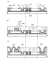
801 光電変換回路部
101B 光センサ
101G 光センサ
101R 光センサ
102B 光電流変換回路部
102G 光電流変換回路部
102R 光電流変換回路部
103B 光フィルタ
103G 光フィルタ
103R 光フィルタ
114B 透光性基板
114G 透光性基板
114R 透光性基板
116B 遮光層
116G 遮光層
116R 遮光層
117B 透光性樹脂層
117G 透光性樹脂層
117R 透光性樹脂層
1200 透光性基板
1202 透光性基板
1203 固定テープ
1204 ダイサー
1205 透光性基板
1207 透光性樹脂層
1208 ダイサー
1210 透光性樹脂層
1211 固定テープ
1213 透光性樹脂層
1214 透光性樹脂層
130B 樹脂
130G 樹脂
130R 樹脂
1309 透光性基板
1310 透光性基板
1312 下地絶縁膜
1313 ゲート絶縁膜
1314 配線
1316 層間絶縁膜
1317 層間絶縁膜
1318 保護電極
1319 配線
1320 接続電極
1324 封止層
1331 半導体層
1334 ゲート電極
1337 ドレイン領域
1341 ドレイン電極
1345 保護電極
1346 保護電極
1348 保護電極
1350 端子電極
1351 端子電極
1360 インターポーザ
1361 電極
1362 電極
1371 光電変換層
1371i i型半導体層
1371n n型半導体層
1371p p型半導体層
1373 トランジスタ
1374 配線
1375 配線
1377 保護膜
1378 封止膜
1601 透光性基板
1602 単結晶半導体層
1604 絶縁層
1608 単結晶半導体基板
1609 ブロッキング層
1610 脆弱化層
1621 保護層
1801 本体(A)
1802 本体(B)
1803 筐体
1804 操作キー
1805 音声出力部
1806 音声入力部
1807 回路基板
1808 表示パネル(A)
1809 表示パネル(B)
1811 透光性材料部
1812 センサ
1812 カラーセンサ
1810 蝶番
1821 本体
1822 筐体
1823 表示パネル
1824 操作キー
1825 音声出力部
1826 音声入力部
1827 カラーセンサ
1828 カラーセンサ
1831 本体
1832 筐体
1833 表示部
1834 キーボード
1835 外部接続ポート
1836 ポインティングデバイス
1841 筐体
1842 支持台
1843 表示部
1852 液晶層
1853 バックライト
1854A カラーセンサ
1854B カラーセンサ
1862 液晶パネル
202A 端子
202B 端子
202C 端子
202D 端子
2101 リリースボタン
2102 メインスイッチ
2103 ファインダ窓
2104 フラッシュ
2105 レンズ
2106 鏡胴
2107 筺体
2110 カラーセンサ
2111 ファインダ接眼窓
2112 モニタ
2113 操作ボタン
2201A 配線
2201B 配線
2201C 配線
2201D 配線
2201E 配線
2202A 電極
2202B 電極
2202C 電極
2202D 電極
2202E 電極
802A 端子
802B 端子
802C 端子
802D 端子
803A 端子
803B 端子
803C 端子
803D 端子
804A 端子
804B 端子
804C 端子
804D 端子
1012B オームコート
1215a1 端子電極
1215a2 端子電極
1201a 半導体素子層
1206a 溝
1209a 透光性基板
1210a 樹脂層
1212a 光センサ
1214a 透光性樹脂層
1851a 基板
1851b 基板
1852a 偏光フィルタ
1852b 偏光フィルタ
1861A 筐体
1861B 制御回路基板
2113a 操作ボタン
Claims (9)
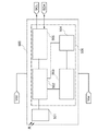
- インターポーザと、第1の光センサと、第2の光センサと、を有し、
前記第1の光センサは、第1の光電流変換回路部と、第1の光フィルタと、を有し、
前記第2の光センサは、第2の光電流変換回路部と、第2の光フィルタと、を有し、
前記第1の光電流変換回路部及び前記第2の光電流変換回路部は、前記インターポーザの表面側に設けられた配線と電気的に接続され、
前記配線は、前記インターポーザに設けられた開口を介して、前記インターポーザの裏面側に設けられた電極と電気的に接続され、
前記電極は、前記第1の光電流変換回路部及び前記第2の光電流変換回路部と重畳せず、
前記電極は、前記第1の光フィルタと重畳する領域、又は、前記第2の光フィルタと重畳する領域を有することを特徴とするカラーセンサ。 - インターポーザと、第1の光センサと、第2の光センサと、を有し、
前記第1の光センサは、第1の光電流変換回路部と、第1の光フィルタと、を有し、
前記第2の光センサは、第2の光電流変換回路部と、第2の光フィルタと、を有し、
前記第1の光電流変換回路部及び前記第2の光電流変換回路部は、前記インターポーザの表面側に設けられた第1の配線と電気的に接続され、
前記第1の光電流変換回路部及び前記第2の光電流変換回路部は、前記インターポーザの表面側に設けられた第2の配線と電気的に接続され、
前記第1の配線は、前記インターポーザに設けられた第1の開口を介して、前記インターポーザの裏面側に設けられた第1の電極と電気的に接続され、
前記第2の配線は、前記インターポーザに設けられた第2の開口を介して、前記インターポーザの裏面側に設けられた第2の電極と電気的に接続され、
前記第1の電極には、第1の電位が供給され、
前記第2の電極には、第2の電位が供給され、
前記第1の電極は、前記第1の光電流変換回路部及び前記第2の光電流変換回路部と重畳せず、
前記第2の電極は、前記第1の光電流変換回路部及び前記第2の光電流変換回路部と重畳せず、
前記第1の電極は、前記第1の光フィルタと重畳する領域、又は、前記第2の光フィルタと重畳する領域を有し、
前記第2の電極は、前記第1の光フィルタと重畳する領域、又は、前記第2の光フィルタと重畳する領域を有することを特徴とするカラーセンサ。 - インターポーザと、光センサと、を有し、
前記光センサは、第1の光電流変換回路部と、第2の光電流変換回路部と、第1の光フィルタと、第2の光フィルタと、を有し、
前記第1の光電流変換回路部及び前記第2の光電流変換回路部は、前記インターポーザの表面側に設けられた配線と電気的に接続され、
前記配線は、前記インターポーザに設けられた開口を介して、前記インターポーザの裏面側に設けられた電極と電気的に接続され、
前記電極は、前記第1の光電流変換回路部及び前記第2の光電流変換回路部と重畳せず、
前記電極は、前記第1の光フィルタと重畳する領域、又は、前記第2の光フィルタと重畳する領域を有することを特徴とするカラーセンサ。 - インターポーザと、光センサと、を有し、
前記光センサは、第1の光電流変換回路部と、第2の光電流変換回路部と、第1の光フィルタと、第2の光フィルタと、を有し、
前記第1の光電流変換回路部及び前記第2の光電流変換回路部は、前記インターポーザの表面側に設けられた第1の配線と電気的に接続され、
前記第1の光電流変換回路部及び前記第2の光電流変換回路部は、前記インターポーザの表面側に設けられた第2の配線と電気的に接続され、
前記第1の配線は、前記インターポーザに設けられた第1の開口を介して、前記インターポーザの裏面側に設けられた第1の電極と電気的に接続され、
前記第2の配線は、前記インターポーザに設けられた第2の開口を介して、前記インターポーザの裏面側に設けられた第2の電極と電気的に接続され、
前記第1の電極には、第1の電位が供給され、
前記第2の電極には、第2の電位が供給され、
前記第1の電極は、前記第1の光電流変換回路部及び前記第2の光電流変換回路部と重畳せず、
前記第2の電極は、前記第1の光電流変換回路部及び前記第2の光電流変換回路部と重畳せず、
前記第1の電極は、前記第1の光フィルタと重畳する領域、又は、前記第2の光フィルタと重畳する領域を有し、
前記第2の電極は、前記第1の光フィルタと重畳する領域、又は、前記第2の光フィルタと重畳する領域を有することを特徴とするカラーセンサ。 - 請求項2又は4において、
前記インターポーザは、前記第1の配線及び第2の配線と電気的に接続されていない第3の配線、又は、前記第1の電極及び前記第2の電極と電気的に接続されていない第3の電極を有することを特徴とするカラーセンサ。 - 請求項1乃至5のいずれか一項にいて、
前記第1の光フィルタ及び前記第2の光フィルタは、透光性を有する樹脂に覆われていることを特徴とするカラーセンサ。 - 請求項1乃至6のいずれか一項において、
前記第1の光電流変換回路部及び前記第2の光電流変換回路部は、光電変換素子からの信号を対数圧縮することができる機能を有することを特徴とするカラーセンサ。 - 請求項1乃至6のいずれか一項において、
前記第1の光電流変換回路部及び前記第2の光電流変換回路部は、光電変換素子からの信号をデジタル信号に変換することができる機能を有することを特徴とするカラーセンサ。 - 請求項1乃至8のいずれか一項に記載のカラーセンサを有することを特徴とする電子機器。
Priority Applications (1)
| Application Number | Priority Date | Filing Date | Title |
|---|---|---|---|
| JP2009158854A JP5518381B2 (ja) | 2008-07-10 | 2009-07-03 | カラーセンサ及び当該カラーセンサを具備する電子機器 |
Applications Claiming Priority (3)
| Application Number | Priority Date | Filing Date | Title |
|---|---|---|---|
| JP2008180776 | 2008-07-10 | ||
| JP2008180776 | 2008-07-10 | ||
| JP2009158854A JP5518381B2 (ja) | 2008-07-10 | 2009-07-03 | カラーセンサ及び当該カラーセンサを具備する電子機器 |
Publications (3)
| Publication Number | Publication Date |
|---|---|
| JP2010041043A JP2010041043A (ja) | 2010-02-18 |
| JP2010041043A5 JP2010041043A5 (ja) | 2012-08-16 |
| JP5518381B2 true JP5518381B2 (ja) | 2014-06-11 |
Family
ID=41504284
Family Applications (1)
| Application Number | Title | Priority Date | Filing Date |
|---|---|---|---|
| JP2009158854A Expired - Fee Related JP5518381B2 (ja) | 2008-07-10 | 2009-07-03 | カラーセンサ及び当該カラーセンサを具備する電子機器 |
Country Status (3)
| Country | Link |
|---|---|
| US (2) | US8502131B2 (ja) |
| JP (1) | JP5518381B2 (ja) |
| KR (2) | KR101605026B1 (ja) |
Families Citing this family (8)
| Publication number | Priority date | Publication date | Assignee | Title |
|---|---|---|---|---|
| US7923800B2 (en) * | 2006-12-27 | 2011-04-12 | Semiconductor Energy Laboratory Co., Ltd. | Semiconductor device and electronic device |
| US9262968B2 (en) * | 2012-10-10 | 2016-02-16 | Canon Kabushiki Kaisha | Image display apparatus and control method thereof |
| US9192029B2 (en) * | 2013-03-14 | 2015-11-17 | Abl Ip Holding Llc | Adaptive optical distribution system |
| EP3466185B1 (en) * | 2016-05-31 | 2021-09-22 | Telefonaktiebolaget LM Ericsson (publ) | Icn connectivity awareness |
| JP6887307B2 (ja) * | 2017-05-19 | 2021-06-16 | ルネサスエレクトロニクス株式会社 | 半導体装置の製造方法 |
| CN108550598B (zh) * | 2018-06-01 | 2019-08-30 | 京东方科技集团股份有限公司 | 电子成像装置及其制备方法、柔性电子复眼及其制备方法 |
| CN109164103A (zh) * | 2018-11-20 | 2019-01-08 | 扬州工业职业技术学院 | 一种稀土金属掺杂高灵敏度的快速检测牛奶中三聚氰胺的试纸 |
| CN110047804B (zh) * | 2019-04-30 | 2021-08-03 | 京东方科技集团股份有限公司 | 阵列基板及制作方法、显示面板、拼接屏 |
Family Cites Families (36)
| Publication number | Priority date | Publication date | Assignee | Title |
|---|---|---|---|---|
| US721455A (en) * | 1902-08-26 | 1903-02-24 | Hugh Watson Mackenzie | Apparatus for baking wafers, &c. |
| JP2653099B2 (ja) * | 1988-05-17 | 1997-09-10 | セイコーエプソン株式会社 | アクティブマトリクスパネル,投写型表示装置及びビューファインダー |
| JPH0676926B2 (ja) * | 1989-06-13 | 1994-09-28 | 三菱電機株式会社 | カラーフィルタ装置 |
| US5468681A (en) * | 1989-08-28 | 1995-11-21 | Lsi Logic Corporation | Process for interconnecting conductive substrates using an interposer having conductive plastic filled vias |
| US5261156A (en) * | 1991-02-28 | 1993-11-16 | Semiconductor Energy Laboratory Co., Ltd. | Method of electrically connecting an integrated circuit to an electric device |
| JP2564728B2 (ja) | 1991-02-28 | 1996-12-18 | 株式会社半導体エネルギー研究所 | 半導体集積回路チップの実装方法 |
| JPH0677510A (ja) * | 1992-08-24 | 1994-03-18 | Canon Inc | 光起電力素子 |
| JP3406727B2 (ja) | 1995-03-10 | 2003-05-12 | 株式会社半導体エネルギー研究所 | 表示装置 |
| US5757456A (en) * | 1995-03-10 | 1998-05-26 | Semiconductor Energy Laboratory Co., Ltd. | Display device and method of fabricating involving peeling circuits from one substrate and mounting on other |
| US5834327A (en) * | 1995-03-18 | 1998-11-10 | Semiconductor Energy Laboratory Co., Ltd. | Method for producing display device |
| JP3638656B2 (ja) | 1995-03-18 | 2005-04-13 | 株式会社半導体エネルギー研究所 | 表示装置及びその作製方法 |
| JPH11160734A (ja) * | 1997-11-28 | 1999-06-18 | Semiconductor Energy Lab Co Ltd | 液晶電気光学装置 |
| JP2001064029A (ja) | 1999-08-27 | 2001-03-13 | Toyo Commun Equip Co Ltd | 多層ガラス基板及び、その切断方法 |
| US6882012B2 (en) * | 2000-02-28 | 2005-04-19 | Semiconductor Energy Laboratory Co., Ltd. | Semiconductor device and a method of manufacturing the same |
| JP2002329576A (ja) * | 2001-04-27 | 2002-11-15 | Semiconductor Energy Lab Co Ltd | 発光装置およびその作製方法 |
| CN100487898C (zh) | 2001-11-05 | 2009-05-13 | 佐伊科比株式会社 | 固体图像传感器及其制造方法 |
| JP2003255386A (ja) | 2002-03-01 | 2003-09-10 | Matsushita Electric Ind Co Ltd | 液晶表示装置 |
| JP2003338519A (ja) * | 2002-05-21 | 2003-11-28 | Renesas Technology Corp | 半導体装置及びその製造方法 |
| US7056810B2 (en) | 2002-12-18 | 2006-06-06 | Semiconductor Energy Laboratory Co., Ltd. | Method for manufacturing semiconductor apparatus, and semiconductor apparatus and electric appliance |
| JP2004207277A (ja) * | 2002-12-20 | 2004-07-22 | Sanyo Electric Co Ltd | 回路装置およびその製造方法 |
| EP1434264A3 (en) * | 2002-12-27 | 2017-01-18 | Semiconductor Energy Laboratory Co., Ltd. | Semiconductor device and manufacturing method using the transfer technique |
| JP2004265889A (ja) * | 2003-01-16 | 2004-09-24 | Tdk Corp | 光電変換素子、光電変換装置、及び鉄シリサイド膜 |
| US8704803B2 (en) * | 2004-08-27 | 2014-04-22 | Semiconductor Energy Laboratory Co., Ltd. | Display device and electronic appliance using the display device |
| KR101058458B1 (ko) | 2004-09-22 | 2011-08-24 | 엘지디스플레이 주식회사 | 저분자 유기 반도체물질을 이용한 액정표시장치용 어레이기판 및 그의 제조 방법 |
| US20060091300A1 (en) * | 2004-10-29 | 2006-05-04 | Nishimura Ken A | Optical color sensor using diffractive elements |
| DE102005023947B4 (de) * | 2005-05-20 | 2007-04-05 | Infineon Technologies Ag | Verfahren zur Herstellung eines optoelektronischen Halbleiterbauteils mit optisch transparenter Abdeckung |
| US8153511B2 (en) * | 2005-05-30 | 2012-04-10 | Semiconductor Energy Laboratory Co., Ltd. | Method for manufacturing semiconductor device |
| US8053816B2 (en) | 2006-03-10 | 2011-11-08 | Semiconductor Energy Laboratory Co., Ltd. | Semiconductor device |
| JP5137418B2 (ja) * | 2006-03-10 | 2013-02-06 | 株式会社半導体エネルギー研究所 | 半導体装置 |
| JP2007310628A (ja) * | 2006-05-18 | 2007-11-29 | Hitachi Displays Ltd | 画像表示装置 |
| JP2007335607A (ja) * | 2006-06-14 | 2007-12-27 | Sharp Corp | Icチップ実装パッケージ、及びこれを用いた画像表示装置 |
| JP4201808B2 (ja) * | 2006-11-08 | 2008-12-24 | シャープ株式会社 | 光電流検出回路ならびにそれを備えた光センサおよび電子機器 |
| KR101441346B1 (ko) | 2007-04-27 | 2014-09-18 | 가부시키가이샤 한도오따이 에네루기 켄큐쇼 | 반도체 장치 및 그 제작 방법 |
| JP5376961B2 (ja) * | 2008-02-01 | 2013-12-25 | 株式会社半導体エネルギー研究所 | 半導体装置 |
| US8049292B2 (en) | 2008-03-27 | 2011-11-01 | Semiconductor Energy Laboratory Co., Ltd. | Semiconductor device and method for manufacturing semiconductor device |
| JP4688229B2 (ja) * | 2008-10-03 | 2011-05-25 | 東芝モバイルディスプレイ株式会社 | 表示装置 |
-
2009
- 2009-07-03 JP JP2009158854A patent/JP5518381B2/ja not_active Expired - Fee Related
- 2009-07-07 US US12/498,662 patent/US8502131B2/en active Active
- 2009-07-10 KR KR1020090063027A patent/KR101605026B1/ko active Application Filing
-
2013
- 2013-08-05 US US13/959,044 patent/US9804080B2/en active Active
-
2016
- 2016-03-14 KR KR1020160030273A patent/KR101644414B1/ko active IP Right Grant
Also Published As
| Publication number | Publication date |
|---|---|
| KR20160037856A (ko) | 2016-04-06 |
| US20130313670A1 (en) | 2013-11-28 |
| KR101644414B1 (ko) | 2016-08-01 |
| US20100006746A1 (en) | 2010-01-14 |
| KR20100007796A (ko) | 2010-01-22 |
| KR101605026B1 (ko) | 2016-03-21 |
| US9804080B2 (en) | 2017-10-31 |
| JP2010041043A (ja) | 2010-02-18 |
| US8502131B2 (en) | 2013-08-06 |
Similar Documents
| Publication | Publication Date | Title |
|---|---|---|
| JP5317712B2 (ja) | 半導体装置及び半導体装置の作製方法 | |
| JP5376961B2 (ja) | 半導体装置 | |
| JP5433272B2 (ja) | 半導体装置及び半導体装置の作製方法 | |
| JP5518381B2 (ja) | カラーセンサ及び当該カラーセンサを具備する電子機器 | |
| TWI480984B (zh) | 半導體裝置以及半導體裝置的製造方法 | |
| JP5587558B2 (ja) | 光電変換装置 | |
| KR20060120492A (ko) | 광전 변환 디바이스, 그 제조 방법 및 반도체 디바이스 | |
| JP4809715B2 (ja) | 光電変換装置及びその作製方法、並びに半導体装置 | |
| JP2009177160A (ja) | 半導体装置及び半導体装置の作製方法 | |
| JP5303161B2 (ja) | 半導体装置の作製方法 | |
| US7679091B2 (en) | Photoelectric conversion element having a semiconductor and semiconductor device using the same |
Legal Events
| Date | Code | Title | Description |
|---|---|---|---|
| A521 | Request for written amendment filed |
Free format text: JAPANESE INTERMEDIATE CODE: A523 Effective date: 20120702 |
|
| A621 | Written request for application examination |
Free format text: JAPANESE INTERMEDIATE CODE: A621 Effective date: 20120702 |
|
| A977 | Report on retrieval |
Free format text: JAPANESE INTERMEDIATE CODE: A971007 Effective date: 20130917 |
|
| A131 | Notification of reasons for refusal |
Free format text: JAPANESE INTERMEDIATE CODE: A131 Effective date: 20130924 |
|
| A521 | Request for written amendment filed |
Free format text: JAPANESE INTERMEDIATE CODE: A523 Effective date: 20131001 |
|
| TRDD | Decision of grant or rejection written | ||
| A01 | Written decision to grant a patent or to grant a registration (utility model) |
Free format text: JAPANESE INTERMEDIATE CODE: A01 Effective date: 20140304 |
|
| A61 | First payment of annual fees (during grant procedure) |
Free format text: JAPANESE INTERMEDIATE CODE: A61 Effective date: 20140402 |
|
| R150 | Certificate of patent or registration of utility model |
Ref document number: 5518381 Country of ref document: JP Free format text: JAPANESE INTERMEDIATE CODE: R150 |
|
| R250 | Receipt of annual fees |
Free format text: JAPANESE INTERMEDIATE CODE: R250 |
|
| R250 | Receipt of annual fees |
Free format text: JAPANESE INTERMEDIATE CODE: R250 |
|
| R250 | Receipt of annual fees |
Free format text: JAPANESE INTERMEDIATE CODE: R250 |
|
| R250 | Receipt of annual fees |
Free format text: JAPANESE INTERMEDIATE CODE: R250 |
|
| R250 | Receipt of annual fees |
Free format text: JAPANESE INTERMEDIATE CODE: R250 |
|
| R250 | Receipt of annual fees |
Free format text: JAPANESE INTERMEDIATE CODE: R250 |
|
| LAPS | Cancellation because of no payment of annual fees |