JP5459904B2 - Semiconductor device - Google Patents
Semiconductor device Download PDFInfo
- Publication number
- JP5459904B2 JP5459904B2 JP2009207130A JP2009207130A JP5459904B2 JP 5459904 B2 JP5459904 B2 JP 5459904B2 JP 2009207130 A JP2009207130 A JP 2009207130A JP 2009207130 A JP2009207130 A JP 2009207130A JP 5459904 B2 JP5459904 B2 JP 5459904B2
- Authority
- JP
- Japan
- Prior art keywords
- layer
- thin film
- film transistor
- light
- wiring
- Prior art date
- Legal status (The legal status is an assumption and is not a legal conclusion. Google has not performed a legal analysis and makes no representation as to the accuracy of the status listed.)
- Active
Links
- 239000004065 semiconductor Substances 0.000 title claims description 157
- 239000001301 oxygen Substances 0.000 claims description 49
- 229910052760 oxygen Inorganic materials 0.000 claims description 49
- QVGXLLKOCUKJST-UHFFFAOYSA-N atomic oxygen Chemical compound [O] QVGXLLKOCUKJST-UHFFFAOYSA-N 0.000 claims description 33
- 230000006870 function Effects 0.000 claims description 21
- 239000013078 crystal Substances 0.000 claims description 18
- 229910052751 metal Inorganic materials 0.000 claims description 17
- 239000002184 metal Substances 0.000 claims description 17
- 239000010410 layer Substances 0.000 description 339
- 239000010408 film Substances 0.000 description 221
- 239000010409 thin film Substances 0.000 description 198
- 239000000758 substrate Substances 0.000 description 81
- 238000000034 method Methods 0.000 description 58
- 239000004973 liquid crystal related substance Substances 0.000 description 49
- 238000004544 sputter deposition Methods 0.000 description 38
- 239000000463 material Substances 0.000 description 37
- XKRFYHLGVUSROY-UHFFFAOYSA-N Argon Chemical compound [Ar] XKRFYHLGVUSROY-UHFFFAOYSA-N 0.000 description 35
- 230000015572 biosynthetic process Effects 0.000 description 26
- 239000011159 matrix material Substances 0.000 description 22
- 230000001681 protective effect Effects 0.000 description 22
- 239000003990 capacitor Substances 0.000 description 20
- 238000005530 etching Methods 0.000 description 20
- 239000000123 paper Substances 0.000 description 20
- 229910052786 argon Inorganic materials 0.000 description 19
- 239000007789 gas Substances 0.000 description 19
- 238000005401 electroluminescence Methods 0.000 description 17
- 238000004519 manufacturing process Methods 0.000 description 16
- 238000009832 plasma treatment Methods 0.000 description 15
- 230000008569 process Effects 0.000 description 15
- XLOMVQKBTHCTTD-UHFFFAOYSA-N Zinc monoxide Chemical compound [Zn]=O XLOMVQKBTHCTTD-UHFFFAOYSA-N 0.000 description 14
- 239000002245 particle Substances 0.000 description 14
- 239000010936 titanium Chemical group 0.000 description 14
- 229910052782 aluminium Chemical group 0.000 description 13
- 238000010438 heat treatment Methods 0.000 description 12
- 229920005989 resin Polymers 0.000 description 12
- 239000011347 resin Substances 0.000 description 12
- XAGFODPZIPBFFR-UHFFFAOYSA-N aluminium Chemical group [Al] XAGFODPZIPBFFR-UHFFFAOYSA-N 0.000 description 11
- MYMOFIZGZYHOMD-UHFFFAOYSA-N Dioxygen Chemical compound O=O MYMOFIZGZYHOMD-UHFFFAOYSA-N 0.000 description 10
- 239000004020 conductor Substances 0.000 description 10
- 229910001882 dioxygen Inorganic materials 0.000 description 10
- 229910052733 gallium Inorganic materials 0.000 description 10
- 229910052738 indium Inorganic materials 0.000 description 10
- 238000000206 photolithography Methods 0.000 description 10
- 239000011521 glass Substances 0.000 description 9
- 239000003094 microcapsule Substances 0.000 description 9
- 229910052725 zinc Inorganic materials 0.000 description 9
- 239000011701 zinc Substances 0.000 description 9
- 229910052581 Si3N4 Inorganic materials 0.000 description 8
- VYPSYNLAJGMNEJ-UHFFFAOYSA-N Silicium dioxide Chemical compound O=[Si]=O VYPSYNLAJGMNEJ-UHFFFAOYSA-N 0.000 description 8
- 239000012298 atmosphere Substances 0.000 description 8
- 230000003287 optical effect Effects 0.000 description 8
- 239000000565 sealant Substances 0.000 description 8
- HQVNEWCFYHHQES-UHFFFAOYSA-N silicon nitride Chemical compound N12[Si]34N5[Si]62N3[Si]51N64 HQVNEWCFYHHQES-UHFFFAOYSA-N 0.000 description 8
- 229910052814 silicon oxide Inorganic materials 0.000 description 8
- 239000000126 substance Substances 0.000 description 8
- 229910052719 titanium Inorganic materials 0.000 description 8
- 238000000151 deposition Methods 0.000 description 7
- 230000008021 deposition Effects 0.000 description 7
- 230000005684 electric field Effects 0.000 description 7
- AMGQUBHHOARCQH-UHFFFAOYSA-N indium;oxotin Chemical compound [In].[Sn]=O AMGQUBHHOARCQH-UHFFFAOYSA-N 0.000 description 7
- 238000003780 insertion Methods 0.000 description 7
- 230000037431 insertion Effects 0.000 description 7
- 230000002829 reductive effect Effects 0.000 description 7
- 239000002356 single layer Substances 0.000 description 7
- 239000011787 zinc oxide Substances 0.000 description 7
- RTAQQCXQSZGOHL-UHFFFAOYSA-N Titanium Chemical group [Ti] RTAQQCXQSZGOHL-UHFFFAOYSA-N 0.000 description 6
- 239000000945 filler Substances 0.000 description 6
- 239000000203 mixture Substances 0.000 description 6
- 229910005191 Ga 2 O 3 Inorganic materials 0.000 description 5
- XUIMIQQOPSSXEZ-UHFFFAOYSA-N Silicon Chemical compound [Si] XUIMIQQOPSSXEZ-UHFFFAOYSA-N 0.000 description 5
- 239000000956 alloy Substances 0.000 description 5
- 229910045601 alloy Inorganic materials 0.000 description 5
- 230000002950 deficient Effects 0.000 description 5
- KPUWHANPEXNPJT-UHFFFAOYSA-N disiloxane Chemical class [SiH3]O[SiH3] KPUWHANPEXNPJT-UHFFFAOYSA-N 0.000 description 5
- 229910003437 indium oxide Inorganic materials 0.000 description 5
- PJXISJQVUVHSOJ-UHFFFAOYSA-N indium(iii) oxide Chemical compound [O-2].[O-2].[O-2].[In+3].[In+3] PJXISJQVUVHSOJ-UHFFFAOYSA-N 0.000 description 5
- 230000002441 reversible effect Effects 0.000 description 5
- 239000010703 silicon Substances 0.000 description 5
- 229910052710 silicon Inorganic materials 0.000 description 5
- 239000012798 spherical particle Substances 0.000 description 5
- 238000001039 wet etching Methods 0.000 description 5
- IJGRMHOSHXDMSA-UHFFFAOYSA-N Atomic nitrogen Chemical compound N#N IJGRMHOSHXDMSA-UHFFFAOYSA-N 0.000 description 4
- GYHNNYVSQQEPJS-UHFFFAOYSA-N Gallium Chemical compound [Ga] GYHNNYVSQQEPJS-UHFFFAOYSA-N 0.000 description 4
- GWEVSGVZZGPLCZ-UHFFFAOYSA-N Titan oxide Chemical compound O=[Ti]=O GWEVSGVZZGPLCZ-UHFFFAOYSA-N 0.000 description 4
- 238000000137 annealing Methods 0.000 description 4
- -1 argon ions Chemical class 0.000 description 4
- 229920001940 conductive polymer Polymers 0.000 description 4
- 238000010586 diagram Methods 0.000 description 4
- 238000001312 dry etching Methods 0.000 description 4
- 239000000428 dust Substances 0.000 description 4
- APFVFJFRJDLVQX-UHFFFAOYSA-N indium atom Chemical compound [In] APFVFJFRJDLVQX-UHFFFAOYSA-N 0.000 description 4
- 239000007788 liquid Substances 0.000 description 4
- 230000007246 mechanism Effects 0.000 description 4
- 239000007769 metal material Substances 0.000 description 4
- QGLKJKCYBOYXKC-UHFFFAOYSA-N nonaoxidotritungsten Chemical compound O=[W]1(=O)O[W](=O)(=O)O[W](=O)(=O)O1 QGLKJKCYBOYXKC-UHFFFAOYSA-N 0.000 description 4
- 229920003023 plastic Polymers 0.000 description 4
- 239000004033 plastic Substances 0.000 description 4
- 229920006267 polyester film Polymers 0.000 description 4
- OGIDPMRJRNCKJF-UHFFFAOYSA-N titanium oxide Inorganic materials [Ti]=O OGIDPMRJRNCKJF-UHFFFAOYSA-N 0.000 description 4
- 229910001930 tungsten oxide Inorganic materials 0.000 description 4
- YVTHLONGBIQYBO-UHFFFAOYSA-N zinc indium(3+) oxygen(2-) Chemical compound [O--].[Zn++].[In+3] YVTHLONGBIQYBO-UHFFFAOYSA-N 0.000 description 4
- 239000004642 Polyimide Substances 0.000 description 3
- HCHKCACWOHOZIP-UHFFFAOYSA-N Zinc Chemical compound [Zn] HCHKCACWOHOZIP-UHFFFAOYSA-N 0.000 description 3
- NIXOWILDQLNWCW-UHFFFAOYSA-N acrylic acid group Chemical group C(C=C)(=O)O NIXOWILDQLNWCW-UHFFFAOYSA-N 0.000 description 3
- 125000004429 atom Chemical group 0.000 description 3
- 239000000969 carrier Substances 0.000 description 3
- 239000011651 chromium Substances 0.000 description 3
- 238000004891 communication Methods 0.000 description 3
- 230000000694 effects Effects 0.000 description 3
- 230000002349 favourable effect Effects 0.000 description 3
- 239000001257 hydrogen Substances 0.000 description 3
- 229910052739 hydrogen Inorganic materials 0.000 description 3
- 229910052750 molybdenum Inorganic materials 0.000 description 3
- 150000002894 organic compounds Chemical class 0.000 description 3
- TWNQGVIAIRXVLR-UHFFFAOYSA-N oxo(oxoalumanyloxy)alumane Chemical compound O=[Al]O[Al]=O TWNQGVIAIRXVLR-UHFFFAOYSA-N 0.000 description 3
- 238000005192 partition Methods 0.000 description 3
- 238000000059 patterning Methods 0.000 description 3
- 229920001721 polyimide Polymers 0.000 description 3
- 229920002620 polyvinyl fluoride Polymers 0.000 description 3
- 230000004044 response Effects 0.000 description 3
- 239000000243 solution Substances 0.000 description 3
- 238000003860 storage Methods 0.000 description 3
- 229910052721 tungsten Inorganic materials 0.000 description 3
- UWCWUCKPEYNDNV-LBPRGKRZSA-N 2,6-dimethyl-n-[[(2s)-pyrrolidin-2-yl]methyl]aniline Chemical compound CC1=CC=CC(C)=C1NC[C@H]1NCCC1 UWCWUCKPEYNDNV-LBPRGKRZSA-N 0.000 description 2
- CURLTUGMZLYLDI-UHFFFAOYSA-N Carbon dioxide Chemical compound O=C=O CURLTUGMZLYLDI-UHFFFAOYSA-N 0.000 description 2
- PXGOKWXKJXAPGV-UHFFFAOYSA-N Fluorine Chemical compound FF PXGOKWXKJXAPGV-UHFFFAOYSA-N 0.000 description 2
- VEXZGXHMUGYJMC-UHFFFAOYSA-N Hydrochloric acid Chemical compound Cl VEXZGXHMUGYJMC-UHFFFAOYSA-N 0.000 description 2
- UFHFLCQGNIYNRP-UHFFFAOYSA-N Hydrogen Chemical compound [H][H] UFHFLCQGNIYNRP-UHFFFAOYSA-N 0.000 description 2
- ZOKXTWBITQBERF-UHFFFAOYSA-N Molybdenum Chemical group [Mo] ZOKXTWBITQBERF-UHFFFAOYSA-N 0.000 description 2
- PXHVJJICTQNCMI-UHFFFAOYSA-N Nickel Chemical group [Ni] PXHVJJICTQNCMI-UHFFFAOYSA-N 0.000 description 2
- 230000001133 acceleration Effects 0.000 description 2
- 125000000217 alkyl group Chemical group 0.000 description 2
- DQXBYHZEEUGOBF-UHFFFAOYSA-N but-3-enoic acid;ethene Chemical compound C=C.OC(=O)CC=C DQXBYHZEEUGOBF-UHFFFAOYSA-N 0.000 description 2
- 230000001413 cellular effect Effects 0.000 description 2
- 229910052804 chromium Inorganic materials 0.000 description 2
- 239000010949 copper Substances 0.000 description 2
- PMHQVHHXPFUNSP-UHFFFAOYSA-M copper(1+);methylsulfanylmethane;bromide Chemical compound Br[Cu].CSC PMHQVHHXPFUNSP-UHFFFAOYSA-M 0.000 description 2
- 238000009792 diffusion process Methods 0.000 description 2
- 230000009977 dual effect Effects 0.000 description 2
- 239000005038 ethylene vinyl acetate Substances 0.000 description 2
- 230000005281 excited state Effects 0.000 description 2
- 230000001747 exhibiting effect Effects 0.000 description 2
- 239000000284 extract Substances 0.000 description 2
- 239000005262 ferroelectric liquid crystals (FLCs) Substances 0.000 description 2
- 239000011152 fibreglass Substances 0.000 description 2
- 238000007667 floating Methods 0.000 description 2
- 239000011737 fluorine Substances 0.000 description 2
- 229910052731 fluorine Inorganic materials 0.000 description 2
- 239000012535 impurity Substances 0.000 description 2
- 238000002347 injection Methods 0.000 description 2
- 239000007924 injection Substances 0.000 description 2
- 150000002500 ions Chemical class 0.000 description 2
- 239000011859 microparticle Substances 0.000 description 2
- 239000011733 molybdenum Chemical group 0.000 description 2
- 229910052757 nitrogen Inorganic materials 0.000 description 2
- 239000011368 organic material Substances 0.000 description 2
- BPUBBGLMJRNUCC-UHFFFAOYSA-N oxygen(2-);tantalum(5+) Chemical compound [O-2].[O-2].[O-2].[O-2].[O-2].[Ta+5].[Ta+5] BPUBBGLMJRNUCC-UHFFFAOYSA-N 0.000 description 2
- 230000003071 parasitic effect Effects 0.000 description 2
- 239000000049 pigment Substances 0.000 description 2
- 229920001200 poly(ethylene-vinyl acetate) Polymers 0.000 description 2
- 229920002037 poly(vinyl butyral) polymer Polymers 0.000 description 2
- 229920000915 polyvinyl chloride Polymers 0.000 description 2
- 239000004800 polyvinyl chloride Substances 0.000 description 2
- 238000001552 radio frequency sputter deposition Methods 0.000 description 2
- 238000005546 reactive sputtering Methods 0.000 description 2
- 230000008707 rearrangement Effects 0.000 description 2
- 239000003566 sealing material Substances 0.000 description 2
- 238000009751 slip forming Methods 0.000 description 2
- 239000002904 solvent Substances 0.000 description 2
- 125000006850 spacer group Chemical group 0.000 description 2
- 125000001424 substituent group Chemical group 0.000 description 2
- 229910052715 tantalum Inorganic materials 0.000 description 2
- 229910001936 tantalum oxide Inorganic materials 0.000 description 2
- 230000007704 transition Effects 0.000 description 2
- WFKWXMTUELFFGS-UHFFFAOYSA-N tungsten Chemical group [W] WFKWXMTUELFFGS-UHFFFAOYSA-N 0.000 description 2
- 239000010937 tungsten Substances 0.000 description 2
- 238000001771 vacuum deposition Methods 0.000 description 2
- 210000003462 vein Anatomy 0.000 description 2
- 239000004925 Acrylic resin Substances 0.000 description 1
- 229920000178 Acrylic resin Polymers 0.000 description 1
- 229910017073 AlLi Inorganic materials 0.000 description 1
- 239000004986 Cholesteric liquid crystals (ChLC) Substances 0.000 description 1
- VYZAMTAEIAYCRO-UHFFFAOYSA-N Chromium Chemical compound [Cr] VYZAMTAEIAYCRO-UHFFFAOYSA-N 0.000 description 1
- RYGMFSIKBFXOCR-UHFFFAOYSA-N Copper Chemical compound [Cu] RYGMFSIKBFXOCR-UHFFFAOYSA-N 0.000 description 1
- 239000004593 Epoxy Substances 0.000 description 1
- 206010052128 Glare Diseases 0.000 description 1
- DGAQECJNVWCQMB-PUAWFVPOSA-M Ilexoside XXIX Chemical compound C[C@@H]1CC[C@@]2(CC[C@@]3(C(=CC[C@H]4[C@]3(CC[C@@H]5[C@@]4(CC[C@@H](C5(C)C)OS(=O)(=O)[O-])C)C)[C@@H]2[C@]1(C)O)C)C(=O)O[C@H]6[C@@H]([C@H]([C@@H]([C@H](O6)CO)O)O)O.[Na+] DGAQECJNVWCQMB-PUAWFVPOSA-M 0.000 description 1
- 229910052779 Neodymium Inorganic materials 0.000 description 1
- CBENFWSGALASAD-UHFFFAOYSA-N Ozone Chemical compound [O-][O+]=O CBENFWSGALASAD-UHFFFAOYSA-N 0.000 description 1
- OAICVXFJPJFONN-UHFFFAOYSA-N Phosphorus Chemical compound [P] OAICVXFJPJFONN-UHFFFAOYSA-N 0.000 description 1
- 239000004952 Polyamide Substances 0.000 description 1
- 229910003902 SiCl 4 Inorganic materials 0.000 description 1
- 229910002808 Si–O–Si Inorganic materials 0.000 description 1
- 229910006404 SnO 2 Inorganic materials 0.000 description 1
- 206010047571 Visual impairment Diseases 0.000 description 1
- GDFCWFBWQUEQIJ-UHFFFAOYSA-N [B].[P] Chemical compound [B].[P] GDFCWFBWQUEQIJ-UHFFFAOYSA-N 0.000 description 1
- 230000002411 adverse Effects 0.000 description 1
- 239000005407 aluminoborosilicate glass Substances 0.000 description 1
- 238000013459 approach Methods 0.000 description 1
- 239000012300 argon atmosphere Substances 0.000 description 1
- 150000004945 aromatic hydrocarbons Chemical class 0.000 description 1
- 125000003118 aryl group Chemical group 0.000 description 1
- 229910052788 barium Inorganic materials 0.000 description 1
- DSAJWYNOEDNPEQ-UHFFFAOYSA-N barium atom Chemical compound [Ba] DSAJWYNOEDNPEQ-UHFFFAOYSA-N 0.000 description 1
- 230000008901 benefit Effects 0.000 description 1
- UMIVXZPTRXBADB-UHFFFAOYSA-N benzocyclobutene Chemical compound C1=CC=C2CCC2=C1 UMIVXZPTRXBADB-UHFFFAOYSA-N 0.000 description 1
- 239000011230 binding agent Substances 0.000 description 1
- 239000005380 borophosphosilicate glass Substances 0.000 description 1
- 239000005388 borosilicate glass Substances 0.000 description 1
- 239000001569 carbon dioxide Substances 0.000 description 1
- 229910002092 carbon dioxide Inorganic materials 0.000 description 1
- 239000000919 ceramic Substances 0.000 description 1
- 238000006243 chemical reaction Methods 0.000 description 1
- 230000003098 cholesteric effect Effects 0.000 description 1
- 239000002131 composite material Substances 0.000 description 1
- 150000001875 compounds Chemical class 0.000 description 1
- 239000000356 contaminant Substances 0.000 description 1
- 238000011109 contamination Methods 0.000 description 1
- 229920001577 copolymer Polymers 0.000 description 1
- 229910052802 copper Inorganic materials 0.000 description 1
- 238000007872 degassing Methods 0.000 description 1
- 238000013461 design Methods 0.000 description 1
- 238000001514 detection method Methods 0.000 description 1
- 230000006866 deterioration Effects 0.000 description 1
- 239000003989 dielectric material Substances 0.000 description 1
- 238000007599 discharging Methods 0.000 description 1
- 238000006073 displacement reaction Methods 0.000 description 1
- 230000005611 electricity Effects 0.000 description 1
- 239000003822 epoxy resin Substances 0.000 description 1
- 239000004744 fabric Substances 0.000 description 1
- 238000010304 firing Methods 0.000 description 1
- 239000011888 foil Substances 0.000 description 1
- 230000005283 ground state Effects 0.000 description 1
- 230000017525 heat dissipation Effects 0.000 description 1
- 239000001307 helium Substances 0.000 description 1
- 229910052734 helium Inorganic materials 0.000 description 1
- SWQJXJOGLNCZEY-UHFFFAOYSA-N helium atom Chemical compound [He] SWQJXJOGLNCZEY-UHFFFAOYSA-N 0.000 description 1
- 230000005525 hole transport Effects 0.000 description 1
- 150000002431 hydrogen Chemical class 0.000 description 1
- 239000011261 inert gas Substances 0.000 description 1
- 150000002484 inorganic compounds Chemical class 0.000 description 1
- 229910010272 inorganic material Inorganic materials 0.000 description 1
- 239000012212 insulator Substances 0.000 description 1
- 230000001678 irradiating effect Effects 0.000 description 1
- 239000000696 magnetic material Substances 0.000 description 1
- 230000005389 magnetism Effects 0.000 description 1
- 238000000838 magnetophoresis Methods 0.000 description 1
- 238000001755 magnetron sputter deposition Methods 0.000 description 1
- 229910021645 metal ion Inorganic materials 0.000 description 1
- 230000004048 modification Effects 0.000 description 1
- 238000012986 modification Methods 0.000 description 1
- QEFYFXOXNSNQGX-UHFFFAOYSA-N neodymium atom Chemical compound [Nd] QEFYFXOXNSNQGX-UHFFFAOYSA-N 0.000 description 1
- 229910052759 nickel Inorganic materials 0.000 description 1
- 150000004767 nitrides Chemical class 0.000 description 1
- 239000012299 nitrogen atmosphere Substances 0.000 description 1
- 238000007645 offset printing Methods 0.000 description 1
- 239000012788 optical film Substances 0.000 description 1
- AHLBNYSZXLDEJQ-FWEHEUNISA-N orlistat Chemical compound CCCCCCCCCCC[C@H](OC(=O)[C@H](CC(C)C)NC=O)C[C@@H]1OC(=O)[C@H]1CCCCCC AHLBNYSZXLDEJQ-FWEHEUNISA-N 0.000 description 1
- 125000004430 oxygen atom Chemical group O* 0.000 description 1
- 229910052698 phosphorus Inorganic materials 0.000 description 1
- 239000011574 phosphorus Substances 0.000 description 1
- 230000010287 polarization Effects 0.000 description 1
- 229920002647 polyamide Polymers 0.000 description 1
- 229920000767 polyaniline Polymers 0.000 description 1
- 229920000647 polyepoxide Polymers 0.000 description 1
- 229920000128 polypyrrole Polymers 0.000 description 1
- 229920001296 polysiloxane Polymers 0.000 description 1
- 229920000123 polythiophene Polymers 0.000 description 1
- 230000005855 radiation Effects 0.000 description 1
- 239000012495 reaction gas Substances 0.000 description 1
- 230000006798 recombination Effects 0.000 description 1
- 238000005215 recombination Methods 0.000 description 1
- 238000007650 screen-printing Methods 0.000 description 1
- 229910052708 sodium Inorganic materials 0.000 description 1
- 239000011734 sodium Substances 0.000 description 1
- 238000004528 spin coating Methods 0.000 description 1
- 238000005507 spraying Methods 0.000 description 1
- 239000010935 stainless steel Substances 0.000 description 1
- 229910001220 stainless steel Inorganic materials 0.000 description 1
- 239000007858 starting material Substances 0.000 description 1
- 230000003068 static effect Effects 0.000 description 1
- 208000024891 symptom Diseases 0.000 description 1
- 230000001360 synchronised effect Effects 0.000 description 1
- GUVRBAGPIYLISA-UHFFFAOYSA-N tantalum atom Chemical compound [Ta] GUVRBAGPIYLISA-UHFFFAOYSA-N 0.000 description 1
- 239000013077 target material Substances 0.000 description 1
- JBQYATWDVHIOAR-UHFFFAOYSA-N tellanylidenegermanium Chemical compound [Te]=[Ge] JBQYATWDVHIOAR-UHFFFAOYSA-N 0.000 description 1
- 229920001187 thermosetting polymer Polymers 0.000 description 1
- 150000003608 titanium Chemical class 0.000 description 1
- 238000002834 transmittance Methods 0.000 description 1
- XLYOFNOQVPJJNP-UHFFFAOYSA-N water Chemical compound O XLYOFNOQVPJJNP-UHFFFAOYSA-N 0.000 description 1
- OYQCBJZGELKKPM-UHFFFAOYSA-N zinc indium(3+) oxygen(2-) Chemical compound [O-2].[Zn+2].[O-2].[In+3] OYQCBJZGELKKPM-UHFFFAOYSA-N 0.000 description 1
Images


Classifications
-
- H—ELECTRICITY
- H01—ELECTRIC ELEMENTS
- H01L—SEMICONDUCTOR DEVICES NOT COVERED BY CLASS H10
- H01L27/00—Devices consisting of a plurality of semiconductor or other solid-state components formed in or on a common substrate
- H01L27/02—Devices consisting of a plurality of semiconductor or other solid-state components formed in or on a common substrate including semiconductor components specially adapted for rectifying, oscillating, amplifying or switching and having at least one potential-jump barrier or surface barrier; including integrated passive circuit elements with at least one potential-jump barrier or surface barrier
- H01L27/12—Devices consisting of a plurality of semiconductor or other solid-state components formed in or on a common substrate including semiconductor components specially adapted for rectifying, oscillating, amplifying or switching and having at least one potential-jump barrier or surface barrier; including integrated passive circuit elements with at least one potential-jump barrier or surface barrier the substrate being other than a semiconductor body, e.g. an insulating body
- H01L27/1214—Devices consisting of a plurality of semiconductor or other solid-state components formed in or on a common substrate including semiconductor components specially adapted for rectifying, oscillating, amplifying or switching and having at least one potential-jump barrier or surface barrier; including integrated passive circuit elements with at least one potential-jump barrier or surface barrier the substrate being other than a semiconductor body, e.g. an insulating body comprising a plurality of TFTs formed on a non-semiconducting substrate, e.g. driving circuits for AMLCDs
- H01L27/124—Devices consisting of a plurality of semiconductor or other solid-state components formed in or on a common substrate including semiconductor components specially adapted for rectifying, oscillating, amplifying or switching and having at least one potential-jump barrier or surface barrier; including integrated passive circuit elements with at least one potential-jump barrier or surface barrier the substrate being other than a semiconductor body, e.g. an insulating body comprising a plurality of TFTs formed on a non-semiconducting substrate, e.g. driving circuits for AMLCDs with a particular composition, shape or layout of the wiring layers specially adapted to the circuit arrangement, e.g. scanning lines in LCD pixel circuits
-
- H—ELECTRICITY
- H01—ELECTRIC ELEMENTS
- H01L—SEMICONDUCTOR DEVICES NOT COVERED BY CLASS H10
- H01L27/00—Devices consisting of a plurality of semiconductor or other solid-state components formed in or on a common substrate
- H01L27/02—Devices consisting of a plurality of semiconductor or other solid-state components formed in or on a common substrate including semiconductor components specially adapted for rectifying, oscillating, amplifying or switching and having at least one potential-jump barrier or surface barrier; including integrated passive circuit elements with at least one potential-jump barrier or surface barrier
- H01L27/12—Devices consisting of a plurality of semiconductor or other solid-state components formed in or on a common substrate including semiconductor components specially adapted for rectifying, oscillating, amplifying or switching and having at least one potential-jump barrier or surface barrier; including integrated passive circuit elements with at least one potential-jump barrier or surface barrier the substrate being other than a semiconductor body, e.g. an insulating body
- H01L27/1214—Devices consisting of a plurality of semiconductor or other solid-state components formed in or on a common substrate including semiconductor components specially adapted for rectifying, oscillating, amplifying or switching and having at least one potential-jump barrier or surface barrier; including integrated passive circuit elements with at least one potential-jump barrier or surface barrier the substrate being other than a semiconductor body, e.g. an insulating body comprising a plurality of TFTs formed on a non-semiconducting substrate, e.g. driving circuits for AMLCDs
- H01L27/1222—Devices consisting of a plurality of semiconductor or other solid-state components formed in or on a common substrate including semiconductor components specially adapted for rectifying, oscillating, amplifying or switching and having at least one potential-jump barrier or surface barrier; including integrated passive circuit elements with at least one potential-jump barrier or surface barrier the substrate being other than a semiconductor body, e.g. an insulating body comprising a plurality of TFTs formed on a non-semiconducting substrate, e.g. driving circuits for AMLCDs with a particular composition, shape or crystalline structure of the active layer
- H01L27/1225—Devices consisting of a plurality of semiconductor or other solid-state components formed in or on a common substrate including semiconductor components specially adapted for rectifying, oscillating, amplifying or switching and having at least one potential-jump barrier or surface barrier; including integrated passive circuit elements with at least one potential-jump barrier or surface barrier the substrate being other than a semiconductor body, e.g. an insulating body comprising a plurality of TFTs formed on a non-semiconducting substrate, e.g. driving circuits for AMLCDs with a particular composition, shape or crystalline structure of the active layer with semiconductor materials not belonging to the group IV of the periodic table, e.g. InGaZnO
-
- H—ELECTRICITY
- H01—ELECTRIC ELEMENTS
- H01L—SEMICONDUCTOR DEVICES NOT COVERED BY CLASS H10
- H01L29/00—Semiconductor devices adapted for rectifying, amplifying, oscillating or switching, or capacitors or resistors with at least one potential-jump barrier or surface barrier, e.g. PN junction depletion layer or carrier concentration layer; Details of semiconductor bodies or of electrodes thereof ; Multistep manufacturing processes therefor
- H01L29/40—Electrodes ; Multistep manufacturing processes therefor
- H01L29/43—Electrodes ; Multistep manufacturing processes therefor characterised by the materials of which they are formed
- H01L29/45—Ohmic electrodes
-
- H—ELECTRICITY
- H01—ELECTRIC ELEMENTS
- H01L—SEMICONDUCTOR DEVICES NOT COVERED BY CLASS H10
- H01L29/00—Semiconductor devices adapted for rectifying, amplifying, oscillating or switching, or capacitors or resistors with at least one potential-jump barrier or surface barrier, e.g. PN junction depletion layer or carrier concentration layer; Details of semiconductor bodies or of electrodes thereof ; Multistep manufacturing processes therefor
- H01L29/66—Types of semiconductor device ; Multistep manufacturing processes therefor
- H01L29/68—Types of semiconductor device ; Multistep manufacturing processes therefor controllable by only the electric current supplied, or only the electric potential applied, to an electrode which does not carry the current to be rectified, amplified or switched
- H01L29/76—Unipolar devices, e.g. field effect transistors
- H01L29/772—Field effect transistors
- H01L29/78—Field effect transistors with field effect produced by an insulated gate
- H01L29/786—Thin film transistors, i.e. transistors with a channel being at least partly a thin film
- H01L29/78606—Thin film transistors, i.e. transistors with a channel being at least partly a thin film with supplementary region or layer in the thin film or in the insulated bulk substrate supporting it for controlling or increasing the safety of the device
- H01L29/78618—Thin film transistors, i.e. transistors with a channel being at least partly a thin film with supplementary region or layer in the thin film or in the insulated bulk substrate supporting it for controlling or increasing the safety of the device characterised by the drain or the source properties, e.g. the doping structure, the composition, the sectional shape or the contact structure
-
- H—ELECTRICITY
- H01—ELECTRIC ELEMENTS
- H01L—SEMICONDUCTOR DEVICES NOT COVERED BY CLASS H10
- H01L29/00—Semiconductor devices adapted for rectifying, amplifying, oscillating or switching, or capacitors or resistors with at least one potential-jump barrier or surface barrier, e.g. PN junction depletion layer or carrier concentration layer; Details of semiconductor bodies or of electrodes thereof ; Multistep manufacturing processes therefor
- H01L29/66—Types of semiconductor device ; Multistep manufacturing processes therefor
- H01L29/68—Types of semiconductor device ; Multistep manufacturing processes therefor controllable by only the electric current supplied, or only the electric potential applied, to an electrode which does not carry the current to be rectified, amplified or switched
- H01L29/76—Unipolar devices, e.g. field effect transistors
- H01L29/772—Field effect transistors
- H01L29/78—Field effect transistors with field effect produced by an insulated gate
- H01L29/786—Thin film transistors, i.e. transistors with a channel being at least partly a thin film
- H01L29/7869—Thin film transistors, i.e. transistors with a channel being at least partly a thin film having a semiconductor body comprising an oxide semiconductor material, e.g. zinc oxide, copper aluminium oxide, cadmium stannate
- H01L29/78693—Thin film transistors, i.e. transistors with a channel being at least partly a thin film having a semiconductor body comprising an oxide semiconductor material, e.g. zinc oxide, copper aluminium oxide, cadmium stannate the semiconducting oxide being amorphous
Description
本発明はチャネル形成領域に酸化物半導体膜を用いた薄膜トランジスタ(以下、TFTという)で構成された回路を有する半導体装置およびその作製方法に関する。例えば、液晶表示パネルに代表される電気光学装置や有機発光素子を有する発光表示装置を部品として搭載した電子機器に関する。 The present invention relates to a semiconductor device having a circuit including a thin film transistor (hereinafter referred to as TFT) using an oxide semiconductor film in a channel formation region and a manufacturing method thereof. For example, the present invention relates to an electronic apparatus in which an electro-optical device typified by a liquid crystal display panel or a light-emitting display device having an organic light-emitting element is mounted as a component.
なお、本明細書中において半導体装置とは、半導体特性を利用することで機能しうる装置全般を指し、電気光学装置、半導体回路および電子機器は全て半導体装置である。 Note that in this specification, a semiconductor device refers to all devices that can function by utilizing semiconductor characteristics, and an electro-optical device, a semiconductor circuit, and an electronic device are all semiconductor devices.
近年、マトリクス状に配置された表示画素毎にTFTからなるスイッチング素子を設けたアクティブマトリクス型の表示装置(液晶表示装置や発光表示装置や電気泳動式表示装置)が盛んに開発されている。アクティブマトリクス型の表示装置は、画素(又は1ドット)毎にスイッチング素子が設けられており、単純マトリクス方式に比べて画素密度が増えた場合に低電圧駆動できるので有利である。 In recent years, active matrix display devices (liquid crystal display devices, light emitting display devices, and electrophoretic display devices) in which switching elements made of TFTs are provided for each display pixel arranged in a matrix have been actively developed. An active matrix display device is advantageous in that a switching element is provided for each pixel (or one dot) and can be driven at a low voltage when the pixel density is increased as compared with the simple matrix method.
また、チャネル形成領域に酸化物半導体膜を用いて薄膜トランジスタ(TFT)などを作製し、電子デバイスや光デバイスに応用する技術が注目されている。例えば、酸化物半導体膜として酸化亜鉛(ZnO)を用いるTFTや、InGaO3(ZnO)mを用いるTFTが挙げられる。これらの酸化物半導体膜を用いたTFTを、透光性を有する基板上に形成し、画像表示装置のスイッチング素子などに用いる技術が特許文献1及び特許文献2で開示されている。
In addition, a technique in which a thin film transistor (TFT) or the like is manufactured using an oxide semiconductor film in a channel formation region and applied to an electronic device or an optical device has attracted attention. For example, a TFT using zinc oxide (ZnO) or a TFT using InGaO 3 (ZnO) m can be given as the oxide semiconductor film.
チャネル形成領域に酸化物半導体膜を用いる薄膜トランジスタには、動作速度が速く、製造工程が比較的簡単であり、十分な信頼性が求められている。 A thin film transistor using an oxide semiconductor film in a channel formation region is required to have high operation speed, a relatively simple manufacturing process, and sufficient reliability.
薄膜トランジスタを形成するにあたり、ソース電極層及びドレイン電極層は、低抵抗な金属材料を用いる。特に、大面積の表示を行う表示装置を製造する際、配線の抵抗による信号の遅延問題が顕著になってくる。従って、配線や電極の材料としては、電気抵抗値の低い金属材料を用いることが望ましい。電気抵抗値の低い金属材料からなるソース電極層及びドレイン電極層と、酸化物半導体膜とが直接接する薄膜トランジスタ構造とすると、コンタクト抵抗が高くなる恐れがある。コンタクト抵抗が高くなる原因は、ソース電極層及びドレイン電極層と、酸化物半導体膜との接触面でショットキー接合が形成されることが要因の一つと考えられる。 In forming the thin film transistor, a low-resistance metal material is used for the source electrode layer and the drain electrode layer. In particular, when manufacturing a display device that displays a large area, a signal delay problem due to the resistance of the wiring becomes remarkable. Therefore, it is desirable to use a metal material having a low electrical resistance value as the material of the wiring and the electrode. When a thin film transistor structure in which a source electrode layer and a drain electrode layer made of a metal material having a low electric resistance value are in direct contact with an oxide semiconductor film, the contact resistance may be increased. One possible cause of the increase in contact resistance is that a Schottky junction is formed at the contact surface between the source and drain electrode layers and the oxide semiconductor film.
加えて、ソース電極層及びドレイン電極層と、酸化物半導体膜とが直接接する部分には容量が形成され、周波数特性(f特性と呼ばれる)が低くなり、薄膜トランジスタの高速動作を妨げる恐れがある。 In addition, a capacitor is formed in a portion where the source electrode layer, the drain electrode layer, and the oxide semiconductor film are in direct contact with each other, frequency characteristics (referred to as f characteristics) are lowered, and high-speed operation of the thin film transistor may be hindered.
本発明の一実施の形態は、インジウム(In)、ガリウム(Ga)、及び亜鉛(Zn)を含む酸化物半導体膜を用いる薄膜トランジスタにおいて、ソース電極層またはドレイン電極層のコンタクト抵抗を低減した薄膜トランジスタ及びその作製方法を提供することを課題の一つとする。 One embodiment of the present invention is a thin film transistor using an oxide semiconductor film containing indium (In), gallium (Ga), and zinc (Zn), in which the contact resistance of the source electrode layer or the drain electrode layer is reduced, and It is an object to provide a manufacturing method thereof.
また、In、Ga、及びZnを含む酸化物半導体膜を用いる薄膜トランジスタの動作特性や信頼性を向上させることも課題の一つとする。 Another object is to improve operating characteristics and reliability of a thin film transistor including an oxide semiconductor film containing In, Ga, and Zn.
また、In、Ga、及びZnを含む酸化物半導体膜を用いる薄膜トランジスタの電気特性のバラツキを低減することも課題の一つとする。特に、液晶表示装置においては、TFT間での電気的特性のバラツキが大きい場合、そのTFT間での電気的特性のバラツキに起因する表示むらが発生する恐れがある。 Another object is to reduce variation in electric characteristics of a thin film transistor including an oxide semiconductor film containing In, Ga, and Zn. In particular, in a liquid crystal display device, when the variation in electrical characteristics between TFTs is large, display unevenness due to the variation in electrical characteristics between the TFTs may occur.
また、発光素子を有する表示装置においても、発光素子に一定の電流が流れるように配置されたTFT(駆動回路または画素に配置される発光素子に電流を供給するTFT)のオン電流(Ion)のバラツキが大きい場合、表示画面において輝度のバラツキが生じる恐れがある。 In a display device having a light-emitting element, an on-current (I on ) of a TFT (a TFT that supplies current to a light-emitting element arranged in a driver circuit or a pixel) arranged so that a constant current flows through the light-emitting element When there is a large variation in brightness, there is a risk of variations in luminance on the display screen.
以上、本発明の一実施の形態は、上記課題の少なくとも一つを解決することを目的とする。 As described above, an embodiment of the present invention aims to solve at least one of the above problems.
本発明の一実施の形態は、ゲート絶縁層上に低抵抗な酸化物半導体層をソース領域またはドレイン領域として形成した後、ドレイン電極層またはソース電極層を形成し、その上に半導体層として非単結晶の酸化物半導体膜を形成する。好ましくは、半導体層として酸素過剰酸化物半導体層を用い、ソース領域及びドレイン領域として酸素欠乏酸化物半導体層を用いる。このソース領域及びドレイン領域の酸素欠乏酸化物半導体層は直径1nm〜10nm、代表的には2nm〜4nm程度の結晶粒を有していてもよい。 In one embodiment of the present invention, after a low-resistance oxide semiconductor layer is formed over a gate insulating layer as a source region or a drain region, a drain electrode layer or a source electrode layer is formed, and a semiconductor layer is not formed over the drain electrode layer or the source electrode layer. A single crystal oxide semiconductor film is formed. Preferably, an oxygen-excess oxide semiconductor layer is used as the semiconductor layer, and an oxygen-deficient oxide semiconductor layer is used as the source region and the drain region. The oxygen-deficient oxide semiconductor layer in the source region and the drain region may have crystal grains with a diameter of 1 nm to 10 nm, typically about 2 nm to 4 nm.
本明細書において、In、Ga、及びZnを含む酸化物半導体膜を用いて形成された半導体層を「IGZO半導体層」とも記す。IGZO半導体層は、非単結晶の半導体層であり、少なくともアモルファス成分を含んでいるものとする。 In this specification, a semiconductor layer formed using an oxide semiconductor film containing In, Ga, and Zn is also referred to as an “IGZO semiconductor layer”. The IGZO semiconductor layer is a non-single-crystal semiconductor layer and includes at least an amorphous component.
ソース電極層とIGZO半導体層とはオーミック性のコンタクトが必要であり、さらに、そのコンタクト抵抗は極力低減することが望まれる。同様に、ドレイン電極層とIGZO半導体層とはオーミック性のコンタクトが必要であり、さらに、そのコンタクト抵抗は極力低減することが望まれる。そこで、ソース電極層及びドレイン電極層とゲート絶縁層の間に、IGZO半導体層よりもキャリア濃度の高いソース領域及びドレイン領域を意図的に設けることによってオーミック性のコンタクトを形成する。ソース領域及びドレイン領域として機能させる低抵抗なIGZO半導体層は、n型の導電型を有し、n+領域とも呼べる。また、ソース領域及びドレイン領域をn+領域と呼ぶ場合、チャネル形成領域として機能させるIGZO半導体層はI型領域とも呼べる。 The source electrode layer and the IGZO semiconductor layer require ohmic contact, and it is desired that the contact resistance be reduced as much as possible. Similarly, an ohmic contact is necessary between the drain electrode layer and the IGZO semiconductor layer, and it is desirable that the contact resistance be reduced as much as possible. Therefore, an ohmic contact is formed by intentionally providing a source region and a drain region having a carrier concentration higher than that of the IGZO semiconductor layer between the source and drain electrode layers and the gate insulating layer. The low-resistance IGZO semiconductor layer that functions as a source region and a drain region has an n-type conductivity and can also be referred to as an n + region. In addition, when the source region and the drain region are referred to as n + regions, the IGZO semiconductor layer functioning as a channel formation region can also be referred to as an I-type region.
本明細書で開示する発明の構成は、絶縁表面上に、ゲート電極と、該ゲート電極上にゲート絶縁層と、該ゲート絶縁層上にソース領域及びドレイン領域と、ソース領域及びドレイン領域上に金属層と、該金属層上に半導体層とを有し、半導体層は、非単結晶の酸化物半導体層であり、且つ、ゲート絶縁層を介してゲート電極と重なり、ソース領域及びドレイン領域は、半導体層の酸素濃度よりも酸素濃度が低く、金属層は、ソース電極層及びドレイン電極層であることを特徴とする半導体装置である。 The structure of the invention disclosed in this specification includes a gate electrode, a gate insulating layer over the gate electrode, a source region and a drain region over the gate insulating layer, and a source region and a drain region over the gate electrode. A metal layer, and a semiconductor layer over the metal layer, the semiconductor layer is a non-single-crystal oxide semiconductor layer, and overlaps with the gate electrode through the gate insulating layer, and the source region and the drain region are The semiconductor device is characterized in that the oxygen concentration is lower than the oxygen concentration of the semiconductor layer, and the metal layer is a source electrode layer and a drain electrode layer.
本発明の一実施の形態は、上記課題の少なくとも一つを解決する。 One embodiment of the present invention solves at least one of the above problems.
上記構成において、ソース領域及びドレイン領域は、インジウム、ガリウム、及び亜鉛を含む酸化物層であり、IGZO半導体層に比べ低抵抗な膜である。また、ソース領域の端面と、該端面と向かい合うドレイン領域の端面は、半導体層と接している。 In the above structure, the source region and the drain region are oxide layers containing indium, gallium, and zinc, and are films having lower resistance than the IGZO semiconductor layer. The end surface of the source region and the end surface of the drain region facing the end surface are in contact with the semiconductor layer.
なお、非単結晶の半導体層、またはソース領域及びドレイン領域としてIn、Ga、及びZnを含む酸化物半導体膜を用いることができる。また、In、Ga、及びZnのいずれか一をタングステン、モリブデン、チタン、ニッケル、又はアルミニウムと置換してもよい。 Note that a non-single-crystal semiconductor layer or an oxide semiconductor film containing In, Ga, and Zn can be used for a source region and a drain region. Further, any one of In, Ga, and Zn may be replaced with tungsten, molybdenum, titanium, nickel, or aluminum.
また、半導体装置の作製方法も本発明の一実施の形態であり、ソース電極層およびドレイン電極層を形成した後、プラズマ処理を行う。さらに、プラズマ処理後に大気に触れることなくスパッタ法で半導体層を成膜する。半導体層の成膜前に被成膜基板が大気に触れた場合、水分などが付着し、界面状態に悪影響を与え、しきい値のバラツキや、電気特性の劣化、ノーマリーオンのTFTになってしまう症状などを引き起こす恐れがある。プラズマ処理は酸素ガスまたはアルゴンガスを用いる。アルゴンガスに代えて他の希ガスを用いてもよい。 Further, a method for manufacturing a semiconductor device is also an embodiment of the present invention, and after the source electrode layer and the drain electrode layer are formed, plasma treatment is performed. Further, a semiconductor layer is formed by a sputtering method without being exposed to the air after the plasma treatment. If the deposition substrate is exposed to the atmosphere before the semiconductor layer is deposited, moisture will adhere to it, adversely affecting the interface state, resulting in variations in threshold values, deterioration of electrical characteristics, and normally-on TFTs. May cause symptoms such as. For the plasma treatment, oxygen gas or argon gas is used. Another rare gas may be used instead of the argon gas.
本明細書で開示する作製方法に関する発明の構成は、絶縁表面上にゲート電極を形成し、ゲート電極上にゲート絶縁層と、該ゲート絶縁層上にソース領域及びドレイン領域と金属層の積層を形成し、金属層を選択的にエッチングしてソース電極層及びドレイン電極層を形成し、露呈しているゲート絶縁層、ソース電極層、及びドレイン電極層にプラズマ処理を行い、ゲート電極と重なり、且つプラズマ処理が施されたゲート絶縁層上に大気にふれることなく半導体層を形成し、半導体層は、非単結晶の酸化物半導体層であり、ソース領域及びドレイン領域は、半導体層の酸素濃度よりも酸素濃度が低いことを特徴とする半導体装置の作製方法である。 In the structure of the invention relating to the manufacturing method disclosed in this specification, a gate electrode is formed over an insulating surface, a gate insulating layer is formed over the gate electrode, and a stack of a source region, a drain region, and a metal layer is formed over the gate insulating layer. And forming a source electrode layer and a drain electrode layer by selectively etching the metal layer, performing plasma treatment on the exposed gate insulating layer, the source electrode layer, and the drain electrode layer, and overlapping with the gate electrode; In addition, a semiconductor layer is formed over the gate insulating layer which has been subjected to plasma treatment without being exposed to the air, the semiconductor layer is a non-single-crystal oxide semiconductor layer, and the source region and the drain region have an oxygen concentration of the semiconductor layer The method for manufacturing a semiconductor device is characterized in that the oxygen concentration is lower than that of the semiconductor device.
プラズマ処理によって、露呈しているゲート絶縁層の表面、及びソース電極層の表面、ドレイン電極層の表面を洗浄することができる。IGZO半導体層の形成よりも先にソース電極層及びドレイン電極層をフォトリソグラフィ技術によってパターニング形成するため、表面に残った有機物と反応させて有機物などのゴミを除去するプラズマ処理を行うことは有用である。 By the plasma treatment, the exposed surface of the gate insulating layer, the surface of the source electrode layer, and the surface of the drain electrode layer can be cleaned. Since the source electrode layer and the drain electrode layer are patterned by photolithography prior to the formation of the IGZO semiconductor layer, it is useful to perform plasma treatment that removes dust such as organic substances by reacting with organic substances remaining on the surface. is there.
特に、プラズマ処理後に大気に触れることなくスパッタ法でIGZO半導体層を成膜するため、IGZO半導体層の成膜と同じチャンバーで行うことが可能な逆スパッタと呼ばれるプラズマ処理の一種を行うことが好ましい。逆スパッタとは、ターゲット側に電圧を印加せずに、酸素、又は酸素及びアルゴン雰囲気下で基板側に電圧を印加して基板にプラズマを形成して表面を改質する方法である。 In particular, since the IGZO semiconductor layer is formed by a sputtering method without exposure to the air after the plasma treatment, it is preferable to perform a kind of plasma treatment called reverse sputtering that can be performed in the same chamber as the formation of the IGZO semiconductor layer. . Reverse sputtering is a method of modifying the surface by forming a plasma on a substrate by applying a voltage to the substrate side in an oxygen or oxygen and argon atmosphere without applying a voltage to the target side.
また、チャンバーに酸素ガスを用いるプラズマ処理を行う場合、ゲート絶縁層表面に酸素ラジカルが照射されることによって、ゲート絶縁層表面を酸素過剰領域に改質し、後に成膜するIGZO半導体層との界面における酸素濃度を高くする。ゲート絶縁層に酸素ラジカル処理を行って半導体層を積層し、熱処理を行えば、IGZO半導体層のゲート絶縁層側の酸素濃度も高濃度とすることができる。従って、ゲート絶縁層とIGZO半導体層との界面に酸素濃度のピークを有し、かつゲート絶縁層の酸素濃度は濃度勾配を有し、その勾配はゲート絶縁層とIGZO半導体層との界面に近づくにつれて増加する。酸素過剰領域を有するゲート絶縁層と酸素過剰酸化物半導体層(IGZO半導体層)は相性がよく、良好な界面特性を得ることができる。 In addition, when performing plasma treatment using oxygen gas in the chamber, the surface of the gate insulating layer is irradiated with oxygen radicals to modify the surface of the gate insulating layer into an oxygen-excess region, and the IGZO semiconductor layer to be formed later Increase the oxygen concentration at the interface. By performing oxygen radical treatment on the gate insulating layer to stack a semiconductor layer and performing heat treatment, the oxygen concentration on the gate insulating layer side of the IGZO semiconductor layer can be increased. Therefore, there is a peak of oxygen concentration at the interface between the gate insulating layer and the IGZO semiconductor layer, and the oxygen concentration of the gate insulating layer has a concentration gradient, and the gradient approaches the interface between the gate insulating layer and the IGZO semiconductor layer. Increases with time. The gate insulating layer having an oxygen-excess region and the oxygen-excess oxide semiconductor layer (IGZO semiconductor layer) are compatible with each other, and favorable interface characteristics can be obtained.
酸素ラジカルは、酸素を含むガスを用いてプラズマ発生装置により供給されてもよいし、又はオゾン発生装置により供給されてもよい。供給された酸素ラジカル又は酸素を薄膜に照射することによって膜表面を改質することができる。 Oxygen radicals may be supplied by a plasma generator using a gas containing oxygen, or may be supplied by an ozone generator. The film surface can be modified by irradiating the thin film with supplied oxygen radicals or oxygen.
また、酸素ラジカル処理に限定されず、アルゴンと酸素のラジカル処理を行ってもよい。アルゴンと酸素のラジカル処理とは、アルゴンガスと酸素ガスを導入してプラズマを発生させて薄膜表面の改質を行うことである。 Moreover, it is not limited to an oxygen radical process, You may perform the radical process of argon and oxygen. The radical treatment of argon and oxygen is to reform the thin film surface by introducing argon gas and oxygen gas to generate plasma.
電界が印加され放電プラズマが発生している反応空間中のAr原子(Ar)は、放電プラズマ中の電子(e)により励起又は電離され、アルゴンラジカル(Ar*)やアルゴンイオン(Ar+)や電子(e)となる。アルゴンラジカル(Ar*)はエネルギーの高い準安定状態にあり、周辺にある同種又は異種の原子と反応し、それらの原子を励起又は電離させて安定状態に戻ろうとして雪崩れ現象的に反応が発生する。その時に周辺に酸素があると、酸素原子(O)が励起又は電離され、酸素ラジカル(O*)や酸素イオン(O+)や酸素(O)となる。その酸素ラジカル(O*)が被処理物である薄膜表面の材料と反応し、表面改質が行われ、表面にある有機物と反応して有機物を除去するプラズマ処理が行われる。なお、アルゴンガスのラジカルは、反応性ガス(酸素ガス)のラジカルと比較して準安定状態が長く維持されるという特徴があり、そのためプラズマを発生させるのにアルゴンガスを用いるのが一般的である。 Ar atoms (Ar) in a reaction space in which an electric field is applied and discharge plasma is generated are excited or ionized by electrons (e) in the discharge plasma, and thus argon radicals (Ar * ), argon ions (Ar + ), It becomes an electron (e). The argon radical (Ar * ) is in a metastable state with high energy, reacts with the same or different atoms in the vicinity, reacts in an avalanche phenomenon to excite or ionize those atoms and return to a stable state. Occur. If oxygen is present at that time, oxygen atoms (O) are excited or ionized to become oxygen radicals (O * ), oxygen ions (O + ), and oxygen (O). The oxygen radical (O * ) reacts with the material on the surface of the thin film that is the object to be processed, surface modification is performed, and plasma treatment is performed to react with the organic substance on the surface and remove the organic substance. In addition, the radical of argon gas is characterized in that the metastable state is maintained longer than the radical of reactive gas (oxygen gas), and therefore it is common to use argon gas to generate plasma. is there.
また、酸素ガスを用いる場合、プラズマ処理の条件によっては、ソース電極層及びドレイン電極層の表面が酸化される。仮にソース電極層及びドレイン電極層の表面が酸化され酸化膜で覆われたとしても、ソース電極層またはドレイン電極層の下に接して設けられたソース領域またはドレイン領域は、後に形成される半導体層と電気的に接続させることができる。この場合には接触面積を増やすため、ソース領域(またはドレイン領域)の端面をソース電極層(またはドレイン電極層)の端面よりも突出させた断面形状とすることが好ましく、ソース領域とドレイン領域の間隔がソース電極層とドレイン電極層との間隔よりも短く設計する。例えば、別々のフォトマスクを用いてソース電極層及びドレイン電極層のパターニングと、ソース領域及びドレイン領域のパターニングを行えばよい。また、こうして得られる薄膜トランジスタのチャネル長Lは、ソース領域とドレイン領域の間隔に相当する。 When oxygen gas is used, the surfaces of the source electrode layer and the drain electrode layer are oxidized depending on the conditions of the plasma treatment. Even if the surfaces of the source electrode layer and the drain electrode layer are oxidized and covered with an oxide film, the source region or the drain region provided below and in contact with the source electrode layer or the drain electrode layer is a semiconductor layer to be formed later. Can be electrically connected. In this case, in order to increase the contact area, the end surface of the source region (or drain region) preferably has a cross-sectional shape protruding from the end surface of the source electrode layer (or drain electrode layer). The distance is designed to be shorter than the distance between the source electrode layer and the drain electrode layer. For example, patterning of the source and drain electrode layers and patterning of the source and drain regions may be performed using separate photomasks. In addition, the channel length L of the thin film transistor thus obtained corresponds to the distance between the source region and the drain region.
また、使用するフォトマスクの枚数を削減するため、ソース電極層及びドレイン電極層のパターニング後に、ソース電極層及びドレイン電極層をマスクとして自己整合的にソース領域とドレイン領域を形成してもよい。この場合、ソース領域(またはドレイン領域)の端面とソース電極層(またはドレイン電極層)の端面がほぼ一致するため、ソース領域とドレイン領域の間隔がソース電極層とドレイン電極層との間隔とほぼ同一となる。また、エッチング条件によってはテーパ形状となり、ソース領域とドレイン領域の間隔がソース電極層とドレイン電極層との間隔よりも短くなる。なお、こうして得られる薄膜トランジスタのチャネル長Lも、ソース領域とドレイン領域の間隔に相当する。 In order to reduce the number of photomasks to be used, the source region and the drain region may be formed in a self-aligning manner using the source electrode layer and the drain electrode layer as a mask after patterning the source electrode layer and the drain electrode layer. In this case, since the end surface of the source region (or drain region) and the end surface of the source electrode layer (or drain electrode layer) substantially coincide with each other, the distance between the source region and the drain region is approximately equal to the distance between the source electrode layer and the drain electrode layer. It will be the same. Further, depending on the etching conditions, the shape is tapered, and the distance between the source region and the drain region is shorter than the distance between the source electrode layer and the drain electrode layer. Note that the channel length L of the thin film transistor thus obtained also corresponds to the distance between the source region and the drain region.
IGZO半導体層、ソース領域及びドレイン領域、ソース電極層及びドレイン電極層はスパッタ法(スパッタリング法)で形成すればよい。 The IGZO semiconductor layer, the source and drain regions, the source electrode layer and the drain electrode layer may be formed by a sputtering method (sputtering method).
スパッタ法にはスパッタ用電源に高周波電源を用いるRFスパッタ法と、DCスパッタ法があり、さらにパルス的にバイアスを与えるパルスDCスパッタ法もある。RFスパッタ法は主に絶縁膜を成膜する場合に用いられ、DCスパッタ法は主に金属膜を成膜する場合に用いられる。 Sputtering methods include an RF sputtering method using a high frequency power source as a sputtering power source and a DC sputtering method, and also a pulsed DC sputtering method that applies a bias in a pulsed manner. The RF sputtering method is mainly used when an insulating film is formed, and the DC sputtering method is mainly used when a metal film is formed.
また、材料の異なるターゲットを複数設置できる多元スパッタ装置もある。多元スパッタ装置は、同一チャンバーで異なる材料膜を積層成膜することも、同一チャンバーで複数種類の材料を同時に放電させて成膜することもできる。 There is also a multi-source sputtering apparatus in which a plurality of targets of different materials can be installed. The multi-source sputtering apparatus can be formed by stacking different material films in the same chamber, or by simultaneously discharging a plurality of types of materials in the same chamber.
また、チャンバー内部に磁石機構を備えたマグネトロンスパッタ法を用いるスパッタ装置や、グロー放電を使わずマイクロ波を用いて発生させたプラズマを用いるECRスパッタ法を用いるスパッタ装置がある。 Further, there is a sputtering apparatus using a magnetron sputtering method having a magnet mechanism inside a chamber, and a sputtering apparatus using an ECR sputtering method using plasma generated using microwaves without using glow discharge.
また、スパッタ法を用いる成膜方法として、成膜中にターゲット物質とスパッタガス成分とを化学反応させてそれらの化合物薄膜を形成するリアクティブスパッタ法や、成膜中に基板にも電圧をかけるバイアススパッタ法もある。 In addition, as a film formation method using a sputtering method, a reactive sputtering method in which a target material and a sputtering gas component are chemically reacted during film formation to form a compound thin film thereof, or a voltage is applied to the substrate during film formation. There is also a bias sputtering method.
これら各種のスパッタ法を用いてIGZO半導体層、ソース領域及びドレイン領域、ソース電極層及びドレイン電極層を形成する。 An IGZO semiconductor layer, a source region and a drain region, a source electrode layer and a drain electrode layer are formed using these various sputtering methods.
また、ソース領域及びドレイン領域は、インジウム、ガリウム、及び亜鉛を含む酸化物層であり、IGZO半導体層の成膜条件とは異なる成膜条件で形成される。ソース領域及びドレイン領域の成膜条件は、成膜直後においてサイズが1nm以上10nm以下の結晶粒を含む条件が含まれる。例えば、In2O3:Ga2O3:ZnO=1:1:1としたターゲットを用い、DCスパッタ法でアルゴンガス流量:酸素流量を2:1の割合でチャンバーに導入する成膜条件、或いはアルゴンガスのみを導入する成膜条件とした場合、成膜直後においてサイズが1nm以上10nm以下の結晶粒を含む膜を得ることがある。なお、In2O3:Ga2O3:ZnO=1:1:1としたターゲットはアモルファス状の酸化物半導体膜を得るために、この比率として意図的に設計したものであるため、ソース領域及びドレイン領域をより結晶性の高い膜を得るためにターゲットの組成比を変更してもよい。プロセスの簡略化、または低コストを実現するためには、同じターゲットを用いて導入ガスを変更するだけでIGZO半導体層に用いる膜と、ソース領域及びドレイン領域に用いる膜とを作り分ける方が好ましい。 The source region and the drain region are oxide layers containing indium, gallium, and zinc and are formed under film formation conditions different from the film formation conditions of the IGZO semiconductor layer. The film formation conditions for the source region and the drain region include a condition including crystal grains having a size of 1 nm to 10 nm immediately after film formation. For example, using a target with In 2 O 3 : Ga 2 O 3 : ZnO = 1: 1: 1, film formation conditions for introducing argon gas flow rate: oxygen flow rate into the chamber at a ratio of 2: 1 by DC sputtering method, Alternatively, in the case where the deposition conditions are such that only argon gas is introduced, a film including crystal grains having a size of 1 nm to 10 nm may be obtained immediately after the deposition. Note that since the target with In 2 O 3 : Ga 2 O 3 : ZnO = 1: 1: 1 was intentionally designed as this ratio in order to obtain an amorphous oxide semiconductor film, the source region Further, the composition ratio of the target may be changed in order to obtain a film with higher crystallinity in the drain region. In order to simplify the process or realize low cost, it is preferable to create a film used for the IGZO semiconductor layer and a film used for the source region and the drain region only by changing the introduced gas using the same target. .
酸素欠乏酸化物半導体層をソース領域またはドレイン領域として積極的に設けることにより、金属層であるソース電極層またはドレイン電極層と、IGZO膜との間を良好な接合としてショットキー接合に比べて熱的にも安定動作を有せしめる。また、チャネルのキャリアを供給する(ソース側)、またはチャネルのキャリアを安定して吸収する(ドレイン側)、または抵抗成分をソース電極層(またはドレイン電極層)との界面に作らないためにも積極的にソース領域またはドレイン領域を設けることは重要である。高いドレイン電圧でも良好な移動度を保持するためにも低抵抗化は重要である。 By actively providing an oxygen-deficient oxide semiconductor layer as a source region or a drain region, a heat-dissipation between the source electrode layer or drain electrode layer, which is a metal layer, and the IGZO film is improved as compared with a Schottky junction. It also has stable operation. In addition, in order not to supply channel carriers (source side), to absorb channel carriers stably (drain side), or to create a resistance component at the interface with the source electrode layer (or drain electrode layer) It is important to positively provide a source region or a drain region. Low resistance is important for maintaining good mobility even at high drain voltages.
また、ソース電極層及びドレイン電極層にチタン膜を用いることが好ましい。例えば、チタン膜、アルミニウム膜、チタン膜の積層を用いると低抵抗であり、かつアルミニウム膜にヒロックが発生しにくい。 In addition, a titanium film is preferably used for the source electrode layer and the drain electrode layer. For example, when a stacked film of a titanium film, an aluminum film, and a titanium film is used, the resistance is low and hillocks are hardly generated in the aluminum film.
また、スパッタ法はターゲットに対して強いエネルギーをArイオンで与えるため、成膜されたIGZO半導体層中には強い歪エネルギーが内在すると考えられる。この歪エネルギーを解放するため200℃〜600℃、代表的には300℃〜500℃の熱処理を行うことが好ましい。この熱処理により原子レベルの再配列が行われる。この熱処理によりキャリアの移動を阻害する歪エネルギーが解放されるため、成膜と熱処理(光アニールも含む)は重要である。 Further, since the sputtering method gives strong energy to the target by Ar ions, it is considered that strong strain energy is inherent in the formed IGZO semiconductor layer. In order to release this strain energy, it is preferable to perform heat treatment at 200 ° C. to 600 ° C., typically 300 ° C. to 500 ° C. This heat treatment causes rearrangement at the atomic level. Film formation and heat treatment (including optical annealing) are important because strain energy that inhibits carrier movement is released by this heat treatment.
光電流が少なく、寄生容量が小さく、または、オンオフ比の高い薄膜トランジスタを得ることができ、良好な動特性を有する薄膜トランジスタを作製できる。また、電気特性が高く信頼性のよい薄膜トランジスタを有する半導体装置を提供することができる。 A thin film transistor with low photocurrent, small parasitic capacitance, or high on / off ratio can be obtained, and a thin film transistor having favorable dynamic characteristics can be manufactured. In addition, a semiconductor device including a thin film transistor with high electrical characteristics and high reliability can be provided.
本発明の実施の形態について、図面を用いて詳細に説明する。但し、本発明は以下の説明に限定されず、本発明の趣旨及びその範囲から逸脱することなくその形態及び詳細を様々に変更し得ることは当業者であれば容易に理解される。従って、本発明は以下に示す実施の形態の記載内容に限定して解釈されるものではない。なお、以下に説明する本発明の構成において、同一部分又は同様な機能を有する部分には同一の符号を異なる図面間で共通して用い、その繰り返しの説明は省略する。 Embodiments of the present invention will be described in detail with reference to the drawings. However, the present invention is not limited to the following description, and it is easily understood by those skilled in the art that modes and details can be variously changed without departing from the spirit and scope of the present invention. Therefore, the present invention should not be construed as being limited to the description of the embodiments below. Note that in structures of the present invention described below, the same portions or portions having similar functions are denoted by the same reference numerals in different drawings, and description thereof is not repeated.
(実施の形態1)
本実施の形態では、薄膜トランジスタ及びその作製工程について、図1乃至図7を用いて説明する。
(Embodiment 1)
In this embodiment, a thin film transistor and a manufacturing process thereof will be described with reference to FIGS.
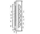
図1(A)において、透光性を有する基板100にはコーニング社の7059ガラスや1737ガラスなどに代表されるバリウムホウケイ酸ガラスやアルミノホウケイ酸ガラスなどのガラス基板を用いることができる。
In FIG. 1A, a glass substrate such as barium borosilicate glass or alumino borosilicate glass typified by Corning 7059 glass or 1737 glass can be used for the light-transmitting
次いで、導電層を基板100全面に形成した後、第1のフォトリソグラフィ工程を行い、レジストマスクを形成し、エッチングにより不要な部分を除去して配線及び電極(ゲート電極101を含むゲート配線、容量配線108、及び第1の端子121)を形成する。このとき少なくともゲート電極101の端部にテーパー形状が形成されるようにエッチングする。この段階での断面図を図1(A)に示した。なお、この段階での上面図が図3に相当する。
Next, after a conductive layer is formed over the entire surface of the
ゲート電極101を含むゲート配線と容量配線108、端子部の第1の端子121は、アルミニウム(Al)や銅(Cu)などの低抵抗導電性材料で形成することが望ましいが、Al単体では耐熱性が劣り、また腐蝕しやすい等の問題点があるので耐熱性導電性材料と組み合わせて形成する。耐熱性導電性材料としては、チタン(Ti)、タンタル(Ta)、タングステン(W)、モリブデン(Mo)、クロム(Cr)、Nd(ネオジム)から選ばれた元素、または上述した元素を成分とする合金か、上述した元素を組み合わせた合金膜、または上述した元素を成分とする窒化物で形成する。
The gate wiring including the
次いで、ゲート電極101上にゲート絶縁層102を全面に成膜する。ゲート絶縁層102はスパッタ法などを用い、膜厚を50〜250nmとする。
Next, a
例えば、ゲート絶縁層102としてスパッタ法により酸化シリコン膜を用い、100nmの厚さで形成する。勿論、ゲート絶縁層102はこのような酸化シリコン膜に限定されるものでなく、酸化窒化シリコン膜、窒化シリコン膜、酸化アルミニウム膜、酸化タンタル膜などの他の絶縁膜を用い、これらの材料から成る単層または積層構造として形成しても良い。
For example, the
次に、ゲート絶縁層102上に第1のIGZO膜をスパッタ法で成膜する。ここでは、In2O3:Ga2O3:ZnO=1:1:1としたターゲットを用い、成膜条件は、圧力を0.4Paとし、電力を500Wとし、成膜温度を室温とし、アルゴンガス流量40sccmを導入してスパッタ成膜を行う。In2O3:Ga2O3:ZnO=1:1:1としたターゲットを意図的に用いているにも関わらず、成膜直後で大きさ1nm〜10nmの結晶粒を含むIGZO膜が形成されることがある。なお、ターゲットの成分比、成膜圧力(0.1Pa〜2.0Pa)、電力(250W〜3000W:8インチφ)、温度(室温〜100℃)、反応性スパッタの成膜条件などを適宜調節することで結晶粒の有無や、結晶粒の密度や、直径サイズは、1nm〜10nmの範囲で調節されうると言える。第1のIGZO膜の膜厚は、5nm〜20nmとする。勿論、膜中に結晶粒が含まれる場合、含まれる結晶粒のサイズが膜厚を超える大きさとならない。本実施の形態では第1のIGZO膜の膜厚は、5nmとする。
Next, a first IGZO film is formed over the
次に、第1のIGZO膜上に金属材料からなる導電膜をスパッタ法や真空蒸着法で形成する。導電膜の材料としては、Al、Cr、Ta、Ti、Mo、Wから選ばれた元素、または上述した元素を成分とする合金か、上述した元素を組み合わせた合金膜等が挙げられる。ここでは、導電膜としてTi膜と、そのTi膜上に重ねてアルミニウム(Al)膜を積層し、さらにその上にTi膜を成膜する3層構造とする。また、導電膜は、2層構造としてもよく、アルミニウム膜上にチタン膜を積層してもよい。また、導電膜は、シリコンを含むアルミニウム膜の単層構造や、チタン膜の単層構造としてもよい。 Next, a conductive film made of a metal material is formed over the first IGZO film by a sputtering method or a vacuum evaporation method. Examples of the material for the conductive film include an element selected from Al, Cr, Ta, Ti, Mo, and W, an alloy containing the above-described element as a component, or an alloy film combining the above-described elements. Here, a Ti film is formed as a conductive film, and an aluminum (Al) film is stacked on the Ti film, and a Ti film is further formed thereon. The conductive film may have a two-layer structure, and a titanium film may be stacked over the aluminum film. The conductive film may have a single-layer structure of an aluminum film containing silicon or a single-layer structure of a titanium film.
ゲート絶縁層、第1のIGZO膜、及び導電膜は、スパッタ法で、チャンバーに導入するガスまたは設置するターゲットを適宜切り替えることにより大気に触れることなく連続成膜することができる。大気に触れることなく連続成膜すると、不純物の混入を防止することができる。大気に触れることなく連続成膜する場合、マルチチャンバー方式の製造装置を用いることが好ましい。 The gate insulating layer, the first IGZO film, and the conductive film can be continuously formed by a sputtering method without being exposed to the air by appropriately switching a gas to be introduced into the chamber or a target to be installed. When a film is continuously formed without being exposed to the atmosphere, contamination of impurities can be prevented. In the case where continuous film formation is performed without exposure to the air, it is preferable to use a multi-chamber manufacturing apparatus.
次に、第2のフォトリソグラフィ工程を行い、レジストマスクを形成し、エッチングにより不要な部分を除去してソース電極層105a及びドレイン電極層105bを形成する。この際のエッチング方法としてウエットエッチングまたはドライエッチングを用いる。ここでは、SiCl4とCl2とBCl3の混合ガスを反応ガスとしたドライエッチングにより、Ti膜とAl膜とTi膜を順次積層した導電膜をエッチングしてソース電極層105a及びドレイン電極層105bを形成する。
Next, a second photolithography step is performed to form a resist mask, and unnecessary portions are removed by etching, so that the
また、この第2のフォトリソグラフィ工程において、ソース電極層105a及びドレイン電極層105bと同じ材料である第2の端子122を端子部に残す。なお、第2の端子122はソース配線(ソース電極層105aを含むソース配線)と電気的に接続されている。
In the second photolithography step, the
次に、ソース電極層105a及びドレイン電極層105bをマスクとして第1のIGZO膜を自己整合的にエッチングする。ここではITO07N(関東化学社製)を用いたウェットエッチングにより、不要な部分を除去してソース領域106a及びドレイン領域106bを形成する。なお、ここでのエッチングは、ウェットエッチングに限定されずドライエッチングを用いてもよい。この段階での断面図を図1(B)に示した。なお、この段階での上面図が図4に相当する。
Next, the first IGZO film is etched in a self-aligned manner using the
また、容量部においては、容量配線108と重なる第1のIGZO膜が除去される。また、端子部においては、第2の端子122の下方に存在し、且つ、第2の端子と重なる第1のIGZO膜130は残存する。
In the capacitor portion, the first IGZO film overlapping the
次に、レジストマスクを除去した後、プラズマ処理を行う。この段階での断面図を図1(C)に示す。ここでは酸素ガスとアルゴンガスを導入してプラズマを発生させる逆スパッタを行い、露出しているゲート絶縁層に酸素ラジカル又は酸素を照射する。こうして、表面に付着しているゴミを除去し、さらにゲート絶縁層表面を酸素過剰領域に改質する。ゲート絶縁層の表面に酸素ラジカル処理を行い、表面を酸素過剰領域とすることは、その後の工程での信頼性向上のための熱処理(200℃〜600℃)において、IGZO半導体層界面の改質のための酸素の供給源を作る上で有効である。 Next, after removing the resist mask, plasma treatment is performed. A cross-sectional view at this stage is illustrated in FIG. Here, reverse sputtering for generating plasma by introducing oxygen gas and argon gas is performed, and the exposed gate insulating layer is irradiated with oxygen radicals or oxygen. In this way, dust adhering to the surface is removed, and the surface of the gate insulating layer is further modified into an oxygen-excess region. Oxygen radical treatment is performed on the surface of the gate insulating layer to make the surface an oxygen-excess region. This is because the heat treatment (200 ° C. to 600 ° C.) for improving the reliability in the subsequent process improves the interface of the IGZO semiconductor layer. It is effective in making a source of oxygen for.
次いで、プラズマ処理後、大気に曝すことなく第2のIGZO膜を成膜する。プラズマ処理後、大気に曝すことなく第2のIGZO膜を成膜することは、ゲート絶縁層と半導体膜の界面にゴミや水分を付着させない点で有用である。ここでは、直径8インチのIn、Ga、及びZnを含む酸化物半導体ターゲット(In2O3:Ga2O3:ZnO=1:1:1)を用いて、基板とターゲットの間との距離を170mm、圧力0.4Pa、直流(DC)電源0.5kW、アルゴン又は酸素雰囲気下で成膜する。なお、パルス直流(DC)電源を用いると、ごみが軽減でき、膜厚分布も均一となるために好ましい。第2のIGZO膜の膜厚は、5nm〜200nmとする。本実施の形態では第2のIGZO膜の膜厚は、100nmとする。 Next, after the plasma treatment, a second IGZO film is formed without being exposed to the atmosphere. After the plasma treatment, forming the second IGZO film without exposure to the air is useful in that dust and moisture are not attached to the interface between the gate insulating layer and the semiconductor film. Here, the distance between the substrate and the target is set using an oxide semiconductor target (In 2 O 3 : Ga 2 O 3 : ZnO = 1: 1: 1) containing In, Ga, and Zn having a diameter of 8 inches. The film is formed in a thickness of 170 mm, a pressure of 0.4 Pa, a direct current (DC) power supply of 0.5 kW, and an argon or oxygen atmosphere. Note that a pulse direct current (DC) power source is preferable because dust can be reduced and the film thickness can be uniform. The thickness of the second IGZO film is 5 nm to 200 nm. In this embodiment mode, the thickness of the second IGZO film is 100 nm.
第2のIGZO膜は、第1のIGZO膜の成膜条件と異ならせることで、第1のIGZO膜の膜中の酸素濃度より多くの酸素を第2のIGZO膜中に含ませる。例えば、第1のIGZO膜の成膜条件における酸素ガス流量の比率よりも第2のIGZO膜の成膜条件における酸素ガス流量の比率が多い条件とする。具体的には、第1のIGZO膜の成膜条件は、希ガス(アルゴン、又はヘリウムなど)雰囲気下(または酸素ガス10%以下、アルゴンガス90%以上)とし、第2のIGZO膜の成膜条件は、酸素雰囲気下(又はアルゴンガス流量は酸素ガス流量率と同じ若しくはそれ以下)とする。多くの酸素を第2のIGZO膜中に含ませることによって、第1のIGZO膜よりも導電率を低くすることができる。また、多くの酸素を第2のIGZO膜中に含ませることによってオフ電流の低減を図ることができるため、オンオフ比の高い薄膜トランジスタを得ることができる。 By making the second IGZO film different from the film formation conditions of the first IGZO film, the second IGZO film contains more oxygen than the oxygen concentration in the film of the first IGZO film. For example, the oxygen gas flow rate ratio in the second IGZO film deposition condition is higher than the oxygen gas flow rate ratio in the first IGZO film deposition condition. Specifically, the first IGZO film is formed under a rare gas (argon or helium) atmosphere (or oxygen gas 10% or less, argon gas 90% or more), and the second IGZO film is formed. The film conditions are under an oxygen atmosphere (or the argon gas flow rate is equal to or less than the oxygen gas flow rate). By including much oxygen in the second IGZO film, the conductivity can be made lower than that of the first IGZO film. In addition, since a large amount of oxygen is contained in the second IGZO film, the off-state current can be reduced, so that a thin film transistor with a high on / off ratio can be obtained.
第2のIGZO膜の成膜は、先に逆スパッタを行ったチャンバーと同一チャンバーを用いてもよいし、大気に曝すことなく成膜できるのであれば、先に逆スパッタを行ったチャンバーと異なるチャンバーで成膜してもよい。 The second IGZO film may be formed in the same chamber as that used for reverse sputtering, or different from the chamber used for reverse sputtering as long as it can be formed without exposure to the atmosphere. The film may be formed in a chamber.
次いで、200℃〜600℃、代表的には300℃〜500℃の熱処理を行うことが好ましい。ここでは炉に入れ、窒素雰囲気下で350℃、1時間の熱処理を行う。この熱処理によりIGZO膜の原子レベルの再配列が行われる。この熱処理によりキャリアの移動を阻害する歪エネルギーが解放されるため、ここでの熱処理(光アニールも含む)は重要である。なお、熱処理を行うタイミングは、第2のIGZO膜の成膜後であれば特に限定されず、例えば画素電極形成後に行ってもよい。 Next, it is preferable to perform heat treatment at 200 ° C. to 600 ° C., typically 300 ° C. to 500 ° C. Here, heat treatment is performed in a furnace at 350 ° C. for 1 hour in a nitrogen atmosphere. By this heat treatment, rearrangement at the atomic level of the IGZO film is performed. The heat treatment (including optical annealing) is important because strain energy that inhibits carrier movement is released by this heat treatment. Note that the timing of performing the heat treatment is not particularly limited as long as it is after the formation of the second IGZO film, and may be performed after the formation of the pixel electrode, for example.
次に、第3のフォトリソグラフィ工程を行い、レジストマスクを形成し、エッチングにより不要な部分を除去してIGZO半導体層103を形成する。以上の工程でIGZO半導体層103をチャネル形成領域とする薄膜トランジスタ170が作製できる。この段階での断面図を図2(A)に示した。なお、この段階での上面図が図5に相当する。ここではITO07N(関東化学社製)を用いたウェットエッチングにより、第2のIGZO膜を除去してIGZO半導体層103を形成する。なお、第1のIGZO膜と第2のIGZO膜のエッチングには同じエッチャントを用いるため、ここでのエッチングにより第1のIGZO膜が除去される。従って、第2のIGZO膜で覆われた第1のIGZO膜の側面は保護されるが、図2(A)に示すように、もう一方の第1のIGZO膜の側面は露呈し、若干エッチングされるため端面の形状が変化する。なお、IGZO半導体層103のエッチングは、ウェットエッチングに限定されずドライエッチングを用いてもよい。
Next, a third photolithography step is performed to form a resist mask, and unnecessary portions are removed by etching, so that the
次いで、レジストマスクを除去し、IGZO半導体層を覆う保護絶縁膜107を形成する。保護絶縁膜107はスパッタ法などを用いて得られる窒化シリコン膜、酸化シリコン膜、酸化窒化シリコン膜、酸化アルミニウム膜、酸化タンタル膜などを用いることができる。
Next, the resist mask is removed, and a protective
次に、第4のフォトリソグラフィ工程を行い、レジストマスクを形成し、保護絶縁膜107のエッチングによりドレイン電極層105bに達するコンタクトホール125を形成する。また、ここでのエッチングにより第2の端子122に達するコンタクトホール127も形成する。なお、マスク数を削減するため、同じレジストマスクを用いてさらにゲート絶縁層をエッチングしてゲート電極に達するコンタクトホール126も形成することが好ましい。この段階での断面図を図2(B)に示す。
Next, a fourth photolithography step is performed to form a resist mask, and a
次いで、レジストマスクを除去した後、透明導電膜を成膜する。透明導電膜の材料としては、酸化インジウム(In2O3)や酸化インジウム酸化スズ合金(In2O3―SnO2、ITOと略記する)などをスパッタ法や真空蒸着法などを用いて形成する。このような材料のエッチング処理は塩酸系の溶液により行う。しかし、特にITOのエッチングは残渣が発生しやすいので、エッチング加工性を改善するために酸化インジウム酸化亜鉛合金(In2O3―ZnO)を用いても良い。 Next, after removing the resist mask, a transparent conductive film is formed. As a material for the transparent conductive film, indium oxide (In 2 O 3 ), an indium tin oxide alloy (In 2 O 3 —SnO 2 , abbreviated as ITO), or the like is formed by a sputtering method, a vacuum evaporation method, or the like. . Etching treatment of such a material is performed with a hydrochloric acid based solution. However, in particular, since etching of ITO is likely to generate a residue, an indium oxide-zinc oxide alloy (In 2 O 3 —ZnO) may be used to improve etching processability.
次に、第5のフォトリソグラフィ工程を行い、レジストマスクを形成し、エッチングにより透明導電膜の不要な部分を除去して画素電極110を形成する。
Next, a fifth photolithography step is performed to form a resist mask, and unnecessary portions of the transparent conductive film are removed by etching to form the
また、この第5のフォトリソグラフィ工程において、容量部におけるゲート絶縁層102及び保護絶縁膜107を誘電体として、容量配線108と画素電極110とで保持容量が形成される。
In the fifth photolithography step, a storage capacitor is formed by the
また、この第5のフォトリソグラフィ工程において、第1の端子及び第2の端子をレジストマスクで覆い端子部に形成された透明導電膜128、129を残す。透明導電膜128、129はFPCとの接続に用いられる電極または配線となる。第2の端子122上に形成された透明導電膜129は、ソース配線の入力端子として機能する接続用の端子電極である。
In the fifth photolithography process, the first terminal and the second terminal are covered with a resist mask, and the transparent
次いで、レジストマスクを除去し、この段階での断面図を図2(C)に示す。なお、この段階での上面図が図6に相当する。 Next, the resist mask is removed, and a cross-sectional view at this stage is illustrated in FIG. Note that a top view at this stage corresponds to FIG.
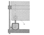
また、図7(A1)、図7(A2)は、この段階でのゲート配線端子部の断面図及び上面図をそれぞれ図示している。図7(A1)は図7(A2)中のC1−C2線に沿った断面図に相当する。図7(A1)において、保護絶縁膜154上に形成される透明導電膜155は、入力端子として機能する接続用の端子電極である。また、図7(A1)において、端子部では、ゲート配線と同じ材料で形成される第1の端子151と、ソース配線と同じ材料で形成される接続電極153とがゲート絶縁層152を介して重なり、透明導電膜155で導通させている。なお、図2(C)に図示した透明導電膜128と第1の端子121とが接触している部分が、図7(A1)の透明導電膜155と第1の端子151が接触している部分に対応している。また、ゲート絶縁層152と接続電極153との間には第1のIGZO膜157が設けられている。
7A1 and 7A2 are a cross-sectional view and a top view of the gate wiring terminal portion at this stage, respectively. FIG. 7A1 corresponds to a cross-sectional view taken along line C1-C2 in FIG. In FIG. 7A1, a transparent
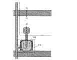
また、図7(B1)、及び図7(B2)は、図2(C)に示すソース配線端子部とは異なるソース配線端子部の断面図及び上面図をそれぞれ図示している。また、図7(B1)は図7(B2)中のD1−D2線に沿った断面図に相当する。図7(B1)において、保護絶縁膜154上に形成される透明導電膜155は、入力端子として機能する接続用の端子電極である。また、図7(B1)において、端子部では、ゲート配線と同じ材料で形成される電極156が、ソース配線と電気的に接続される第2の端子150の下方にゲート絶縁層152を介して重なる。電極156は第2の端子150とは電気的に接続しておらず、電極156を第2の端子150と異なる電位、例えばフローティング、GND、0Vなどに設定すれば、ノイズ対策のための容量または静電気対策のための容量を形成することができる。また、第2の端子150は、保護絶縁膜154を介して透明導電膜155と電気的に接続している。また、ゲート絶縁層152と第2の端子150との間には第1のIGZO膜158が設けられている。
7B1 and 7B2 are a cross-sectional view and a top view of a source wiring terminal portion which is different from the source wiring terminal portion shown in FIG. 2C, respectively. 7B1 corresponds to a cross-sectional view taken along line D1-D2 in FIG. 7B2. In FIG. 7B1, a transparent
ゲート配線、ソース配線、及び容量配線は画素密度に応じて複数本設けられるものである。また、端子部においては、ゲート配線と同電位の第1の端子、ソース配線と同電位の第2の端子、容量配線と同電位の第3の端子などが複数並べられて配置される。それぞれの端子の数は、それぞれ任意な数で設ければ良いものとし、実施者が適宜決定すれば良い。 A plurality of gate wirings, source wirings, and capacitor wirings are provided depending on the pixel density. In the terminal portion, a plurality of first terminals having the same potential as the gate wiring, second terminals having the same potential as the source wiring, third terminals having the same potential as the capacitor wiring, and the like are arranged. An arbitrary number of terminals may be provided, and a practitioner may appropriately determine the number of terminals.
こうして5回のフォトリソグラフィ工程により、5枚のフォトマスクを使用して、ボトムゲート型のnチャネル型TFTである薄膜トランジスタ170を有する画素TFT部、及び保持容量を完成させることができる。そして、これらを個々の画素に対応してマトリクス状に配置して画素部を構成することによりアクティブマトリクス型の表示装置を作製するための一方の基板とすることができる。本明細書では便宜上このような基板をアクティブマトリクス基板と呼ぶ。
In this manner, the pixel TFT portion including the
アクティブマトリクス型の液晶表示装置を作製する場合には、アクティブマトリクス基板と、対向電極が設けられた対向基板との間に液晶層を設け、アクティブマトリクス基板と対向基板とを固定する。なお、対向基板に設けられた対向電極と電気的に接続する共通電極をアクティブマトリクス基板上に設け、共通電極と電気的に接続する第4の端子を端子部に設ける。この第4の端子は、共通電極を固定電位、例えばGND、0Vなどに設定するための端子である。 In the case of manufacturing an active matrix liquid crystal display device, a liquid crystal layer is provided between an active matrix substrate and a counter substrate provided with a counter electrode, and the active matrix substrate and the counter substrate are fixed. Note that a common electrode electrically connected to the counter electrode provided on the counter substrate is provided over the active matrix substrate, and a fourth terminal electrically connected to the common electrode is provided in the terminal portion. The fourth terminal is a terminal for setting the common electrode to a fixed potential such as GND or 0V.
また、本発明の一実施の形態は、図6の画素構成に限定されず、図6とは異なる上面図の例を図8に示す。図8では容量配線を設けず、画素電極を隣り合う画素のゲート配線と保護絶縁膜及びゲート絶縁層を介して重ねて保持容量を形成する例であり、この場合、容量配線及び容量配線と接続する第3の端子は省略することができる。なお、図8において、図6と同じ部分には同じ符号を用いて説明する。 Further, an embodiment of the present invention is not limited to the pixel configuration in FIG. 6, and an example of a top view different from that in FIG. 6 is shown in FIG. FIG. 8 shows an example in which a storage capacitor is formed by overlapping a pixel electrode with a gate wiring of an adjacent pixel through a protective insulating film and a gate insulating layer without providing a capacitor wiring. In this case, the capacitor wiring and the capacitor wiring are connected. The third terminal can be omitted. In FIG. 8, the same parts as those in FIG.
アクティブマトリクス型の液晶表示装置においては、マトリクス状に配置された画素電極を駆動することによって、画面上に表示パターンが形成される。詳しくは選択された画素電極と該画素電極に対応する対向電極との間に電圧が印加されることによって、画素電極と対向電極との間に配置された液晶層の光学変調が行われ、この光学変調が表示パターンとして観察者に認識される。 In an active matrix liquid crystal display device, a display pattern is formed on a screen by driving pixel electrodes arranged in a matrix. Specifically, by applying a voltage between the selected pixel electrode and the counter electrode corresponding to the pixel electrode, optical modulation of the liquid crystal layer disposed between the pixel electrode and the counter electrode is performed. The optical modulation is recognized by the observer as a display pattern.
液晶表示装置の動画表示において、液晶分子自体の応答が遅いため、残像が生じる、または動画のぼけが生じるという問題がある。液晶表示装置の動画特性を改善するため、全面黒表示を1フレームおきに行う、所謂、黒挿入と呼ばれる駆動技術がある。 In moving image display of a liquid crystal display device, there is a problem that an afterimage is generated or a moving image is blurred because the response of the liquid crystal molecules themselves is slow. In order to improve the moving image characteristics of a liquid crystal display device, there is a so-called black insertion driving technique in which black display is performed every other frame.
また、垂直周期を通常の垂直周期の1.5倍以上(好ましくは2倍以上)にすることで動画特性を改善する、所謂、倍速駆動と呼ばれる駆動技術もある。 There is also a so-called double speed drive technique that improves moving image characteristics by making the vertical period 1.5 times or more (preferably twice or more) the normal vertical period.
また、液晶表示装置の動画特性を改善するため、バックライトとして複数のLED(発光ダイオード)光源または複数のEL光源などを用いて面光源を構成し、面光源を構成している各光源を独立して1フレーム基板内で間欠点灯駆動する駆動技術もある。面光源として、3種類以上のLEDを用いてもよいし、白色発光のLEDを用いてもよい。独立して複数のLEDを制御できるため、液晶層の光学変調の切り替えタイミングに合わせてLEDの発光タイミングを同期させることもできる。この駆動技術は、LEDを部分的に消灯することができるため、特に一画面を占める黒い表示領域の割合が多い映像表示の場合には、消費電力の低減効果が図れる。 In addition, in order to improve the moving image characteristics of the liquid crystal display device, a surface light source is configured using a plurality of LED (light emitting diode) light sources or a plurality of EL light sources as a backlight, and each light source constituting the surface light source is independent. There is also a driving technique for intermittently driving within one frame substrate. As the surface light source, three or more kinds of LEDs may be used, or white light emitting LEDs may be used. Since a plurality of LEDs can be controlled independently, the light emission timings of the LEDs can be synchronized with the optical modulation switching timing of the liquid crystal layer. Since this driving technique can partially turn off the LED, an effect of reducing power consumption can be achieved particularly in the case of video display in which the ratio of the black display area occupying one screen is large.
これらの駆動技術を組み合わせることによって、液晶表示装置の動画特性などの表示特性を従来よりも改善することができる。 By combining these driving techniques, the display characteristics such as the moving picture characteristics of the liquid crystal display device can be improved as compared with the related art.
本実施の形態で得られるnチャネル型のトランジスタは、IGZO半導体層をチャネル形成領域に用いており、良好な動特性を有するため、これらの駆動技術を組み合わせることができる。 The n-channel transistor obtained in this embodiment uses an IGZO semiconductor layer for a channel formation region and has favorable dynamic characteristics; therefore, these driving techniques can be combined.
また、発光表示装置を作製する場合、有機発光素子の一方の電極(カソードとも呼ぶ)は、低電源電位、例えばGND、0Vなどに設定するため、端子部に、カソードを低電源電位、例えばGND、0Vなどに設定するための第4の端子が設けられる。また、発光表示装置を作製する場合には、ソース配線、及びゲート配線に加えて電源供給線を設ける。従って、端子部には、電源供給線と電気的に接続する第5の端子を設ける。 In the case of manufacturing a light-emitting display device, one electrode (also referred to as a cathode) of an organic light-emitting element is set to a low power supply potential, for example, GND, 0 V, and the like. , A fourth terminal for setting to 0V or the like is provided. In the case of manufacturing a light-emitting display device, a power supply line is provided in addition to a source wiring and a gate wiring. Therefore, the terminal portion is provided with a fifth terminal that is electrically connected to the power supply line.
(実施の形態2)
本実施の形態では、本発明の一実施の形態の半導体装置として電子ペーパーの例を示す。
(Embodiment 2)
In this embodiment, an example of electronic paper is described as the semiconductor device of one embodiment of the present invention.
図9は、本発明の一実施の形態を適用した半導体装置の例としてアクティブマトリクス型の電子ペーパーを示す。半導体装置に用いられる薄膜トランジスタ581としては、実施の形態1で示す薄膜トランジスタ170と同様に作製でき、酸素ラジカル処理をされたゲート絶縁層と、ソース領域及びドレイン領域上にソース電極層及びドレイン電極層と、ゲート絶縁層、ソース電極層及びドレイン電極層上にIGZO半導体層とを含む電気特性の高い薄膜トランジスタである。
FIG. 9 illustrates active matrix electronic paper as an example of a semiconductor device to which an embodiment of the present invention is applied. A
図9の電子ペーパーは、ツイストボール表示方式を用いた表示装置の例である。ツイストボール表示方式とは、白と黒に塗り分けられた球形粒子を表示素子に用いる電極層である第1の電極層及び第2の電極層の間に配置し、第1の電極層及び第2の電極層に電位差を生じさせて球形粒子の向きを制御することにより、表示を行う方法である。 The electronic paper in FIG. 9 is an example of a display device using a twisting ball display system. The twist ball display method is a method in which spherical particles separately painted in white and black are arranged between a first electrode layer and a second electrode layer which are electrode layers used for a display element, and the first electrode layer and the second electrode layer are arranged. In this method, a potential difference is generated in the two electrode layers to control the orientation of the spherical particles.
基板580と基板596との間に封止される薄膜トランジスタ581はボトムゲート構造の薄膜トランジスタであり、ソース電極層又はドレイン電極層によって第1の電極層587と、絶縁層585に形成する開口で接しており電気的に接続している。第1の電極層587と第2の電極層588との間には黒色領域590a及び白色領域590bを有し、周りに液体で満たされているキャビティ594を含む球形粒子589が設けられており、球形粒子589の周囲は樹脂等の充填材595で充填されている(図9参照。)。
A
また、ツイストボールの代わりに、電気泳動素子を用いることも可能である。透明な液体と、正に帯電した白い微粒子と負に帯電した黒い微粒子とを封入した直径10μm〜200μm程度のマイクロカプセルを用いる。第1の電極層と第2の電極層との間に設けられるマイクロカプセルは、第1の電極層と第2の電極層によって、電場が与えられると、白い微粒子と、黒い微粒子が逆の方向に移動し、白または黒を表示することができる。この原理を応用した表示素子が電気泳動表示素子であり、一般的に電子ペーパーとよばれている。電気泳動表示素子は、液晶表示素子に比べて反射率が高いため、補助ライトは不要であり、また消費電力が小さく、薄暗い場所でも表示部を認識することが可能である。また、表示部に電源が供給されない場合であっても、一度表示した像を保持することが可能であるため、電波発信源から表示機能付き半導体装置(単に表示装置、又は表示装置を具備する半導体装置ともいう)を遠ざけた場合であっても、表示された像を保存しておくことが可能となる。 Further, instead of the twisting ball, an electrophoretic element can be used. A microcapsule having a diameter of about 10 μm to 200 μm in which transparent liquid, positively charged white microparticles, and negatively charged black microparticles are enclosed is used. In the microcapsule provided between the first electrode layer and the second electrode layer, when an electric field is applied by the first electrode layer and the second electrode layer, the white particles and the black particles are in opposite directions. And can display white or black. A display element using this principle is an electrophoretic display element, and is generally called electronic paper. Since the electrophoretic display element has higher reflectance than the liquid crystal display element, an auxiliary light is unnecessary, power consumption is small, and the display portion can be recognized even in a dim place. Further, even when power is not supplied to the display portion, an image once displayed can be held; therefore, a semiconductor device with a display function from a radio wave source (simply a display device or a semiconductor having a display device) Even when the device is also moved away, the displayed image can be stored.
以上の工程により、半導体装置として信頼性の高い電子ペーパーを作製することができる。 Through the above steps, highly reliable electronic paper as a semiconductor device can be manufactured.
本実施の形態は、実施の形態1に記載した構成と適宜組み合わせて実施することが可能である。
This embodiment can be implemented in appropriate combination with the structure described in
(実施の形態3)
本実施の形態では、本発明の一実施の形態の半導体装置の一例である表示装置において、同一基板上に少なくとも駆動回路の一部と、画素部に配置する薄膜トランジスタを作製する例について以下に説明する。
(Embodiment 3)
In this embodiment, an example in which at least part of a driver circuit and a thin film transistor placed in a pixel portion are formed over the same substrate in a display device which is an example of a semiconductor device of one embodiment of the present invention will be described below. To do.
画素部に配置する薄膜トランジスタは、実施の形態1に従って形成する。また、実施の形態1に示す薄膜トランジスタはnチャネル型TFTであるため、駆動回路のうち、nチャネル型TFTで構成することができる駆動回路の一部を画素部の薄膜トランジスタと同一基板上に形成する。
The thin film transistor provided in the pixel portion is formed according to
本発明の一実施の形態の半導体装置の一例であるアクティブマトリクス型液晶表示装置のブロック図の一例を図10(A)に示す。図10(A)に示す表示装置は、基板5300上に表示素子を備えた画素を複数有する画素部5301と、各画素を選択する走査線駆動回路5302と、選択された画素へのビデオ信号の入力を制御する信号線駆動回路5303とを有する。
FIG. 10A illustrates an example of a block diagram of an active matrix liquid crystal display device which is an example of a semiconductor device of one embodiment of the present invention. A display device illustrated in FIG. 10A includes a pixel portion 5301 having a plurality of pixels each provided with a display element over a
また、実施の形態1に示す薄膜トランジスタは、nチャネル型TFTであり、nチャネル型TFTで構成する信号線駆動回路について図11を用いて説明する。
The thin film transistor described in
図11に示す信号線駆動回路は、ドライバIC5601、スイッチ群5602_1〜5602_M、第1の配線5611、第2の配線5612、第3の配線5613及び配線5621_1〜5621_Mを有する。スイッチ群5602_1〜5602_Mそれぞれは、第1の薄膜トランジスタ5603a、第2の薄膜トランジスタ5603b及び第3の薄膜トランジスタ5603cを有する。
The signal line driver circuit illustrated in FIG. 11 includes a
画素部5301は、信号線駆動回路5303から列方向に伸張して配置された複数の信号線S1〜Sm(図示せず。)により信号線駆動回路5303と接続され、走査線駆動回路5302から行方向に伸張して配置された複数の走査線G1〜Gn(図示せず。)により走査線駆動回路5302と接続され、信号線S1〜Sm並びに走査線G1〜Gnに対応してマトリクス状に配置された複数の画素(図示せず。)を有する。そして、各画素は、信号線Sj(信号線S1〜Smのうちいずれか一)、走査線Gi(走査線G1〜Gnのうちいずれか一)と接続される。
The pixel portion 5301 is connected to the signal line driver circuit 5303 by a plurality of signal lines S1 to Sm (not shown) arranged extending from the signal line driver circuit 5303 in the column direction. A plurality of scanning lines G1 to Gn (not shown) arranged in the direction are connected to the scanning
ドライバIC5601は第1の配線5611、第2の配線5612、第3の配線5613及び配線5621_1〜5621_Mに接続される。そして、スイッチ群5602_1〜5602_Mそれぞれは、第1の配線5611、第2の配線5612、第3の配線5613及びスイッチ群5602_1〜5602_Mそれぞれに対応した配線5621_1〜5621_Mに接続される。そして、配線5621_1〜5621_Mそれぞれは、第1の薄膜トランジスタ5603a、第2の薄膜トランジスタ5603b及び第3の薄膜トランジスタ5603cを介して、3つの信号線に接続される。例えば、J列目の配線5621_J(配線5621_1〜配線5621_Mのうちいずれか一)は、スイッチ群5602_Jが有する第1の薄膜トランジスタ5603a、第2の薄膜トランジスタ5603b及び第3の薄膜トランジスタ5603cを介して、信号線Sj−1、信号線Sj、信号線Sj+1に接続される。
The
なお、第1の配線5611、第2の配線5612、第3の配線5613には、それぞれ信号が入力される。
Note that a signal is input to each of the first wiring 5611, the
なお、ドライバIC5601は、単結晶半導体基板上に形成されていることが望ましい。さらに、スイッチ群5602_1〜5602_Mは、画素部と同一基板上に形成されていることが望ましい。したがって、ドライバIC5601とスイッチ群5602_1〜5602_MとはFPCなどを介して接続するとよい。
Note that the
次に、図11に示した信号線駆動回路の動作について、図12のタイミングチャートを参照して説明する。なお、図12のタイミングチャートは、i行目の走査線Giが選択されている場合のタイミングチャートを示している。さらに、i行目の走査線Giの選択期間は、第1のサブ選択期間T1、第2のサブ選択期間T2及び第3のサブ選択期間T3に分割されている。さらに、図11の信号線駆動回路は、他の行の走査線が選択されている場合でも図12と同様の動作をする。 Next, operation of the signal line driver circuit illustrated in FIG. 11 is described with reference to a timing chart of FIG. The timing chart of FIG. 12 shows the timing chart when the i-th scanning line Gi is selected. Further, the selection period of the i-th scanning line Gi is divided into a first sub-selection period T1, a second sub-selection period T2, and a third sub-selection period T3. Further, the signal line driver circuit in FIG. 11 operates in the same manner as in FIG. 12 even when a scan line in another row is selected.
なお、図12のタイミングチャートは、J列目の配線5621_Jが第1の薄膜トランジスタ5603a、第2の薄膜トランジスタ5603b及び第3の薄膜トランジスタ5603cを介して、信号線Sj−1、信号線Sj、信号線Sj+1に接続される場合について示している。
Note that in the timing chart in FIG. 12, the wiring 5621_J in the J-th column is connected to the signal line Sj−1, the signal line Sj, and the signal line Sj + 1 through the first
なお、図12のタイミングチャートは、i行目の走査線Giが選択されるタイミング、第1の薄膜トランジスタ5603aのオン・オフのタイミング5703a、第2の薄膜トランジスタ5603bのオン・オフのタイミング5703b、第3の薄膜トランジスタ5603cのオン・オフのタイミング5703c及びJ列目の配線5621_Jに入力される信号5721_Jを示している。
Note that in the timing chart of FIG. 12, the timing at which the i-th scanning line Gi is selected, the on / off timing 5703a of the first
なお、配線5621_1〜配線5621_Mには第1のサブ選択期間T1、第2のサブ選択期間T2及び第3のサブ選択期間T3において、それぞれ別のビデオ信号が入力される。例えば、第1のサブ選択期間T1において配線5621_Jに入力されるビデオ信号は信号線Sj−1に入力され、第2のサブ選択期間T2において配線5621_Jに入力されるビデオ信号は信号線Sjに入力され、第3のサブ選択期間T3において配線5621_Jに入力されるビデオ信号は信号線Sj+1に入力される。さらに、第1のサブ選択期間T1、第2のサブ選択期間T2及び第3のサブ選択期間T3において、配線5621_Jに入力されるビデオ信号をそれぞれData_j−1、Data_j、Data_j+1とする。
Note that different video signals are input to the wirings 5621_1 to 5621_M in the first sub-selection period T1, the second sub-selection period T2, and the third sub-selection period T3. For example, a video signal input to the wiring 5621_J in the first sub-selection period T1 is input to the signal line Sj-1, and a video signal input to the wiring 5621_J in the second sub-selection period T2 is input to the signal line Sj. Then, the video signal input to the wiring 5621_J in the third sub-selection period T3 is input to the signal
図12に示すように、第1のサブ選択期間T1において第1の薄膜トランジスタ5603aがオンし、第2の薄膜トランジスタ5603b及び第3の薄膜トランジスタ5603cがオフする。このとき、配線5621_Jに入力されるData_j−1が、第1の薄膜トランジスタ5603aを介して信号線Sj−1に入力される。第2のサブ選択期間T2では、第2の薄膜トランジスタ5603bがオンし、第1の薄膜トランジスタ5603a及び第3の薄膜トランジスタ5603cがオフする。このとき、配線5621_Jに入力されるData_jが、第2の薄膜トランジスタ5603bを介して信号線Sjに入力される。第3のサブ選択期間T3では、第3の薄膜トランジスタ5603cがオンし、第1の薄膜トランジスタ5603a及び第2の薄膜トランジスタ5603bがオフする。このとき、配線5621_Jに入力されるData_j+1が、第3の薄膜トランジスタ5603cを介して信号線Sj+1に入力される。
As shown in FIG. 12, in the first sub-selection period T1, the first
以上のことから、図11の信号線駆動回路は、1ゲート選択期間を3つに分割することで、1ゲート選択期間中に1つの配線5621から3つの信号線にビデオ信号を入力することができる。したがって、図11の信号線駆動回路は、ドライバIC5601が形成される基板と、画素部が形成されている基板との接続数を信号線の数に比べて約1/3にすることができる。接続数が約1/3になることによって、図11の信号線駆動回路は、信頼性、歩留まりなどを向上できる。
From the above, the signal line driver circuit in FIG. 11 can divide one gate selection period into three to input video signals from one
なお、図11のように、1ゲート選択期間を複数のサブ選択期間に分割し、複数のサブ選択期間それぞれにおいて、ある1つの配線から複数の信号線それぞれにビデオ信号を入力することができれば、薄膜トランジスタの配置や数、駆動方法などは限定されない。 As shown in FIG. 11, if one gate selection period is divided into a plurality of sub-selection periods, and a video signal can be input from a certain wiring to each of a plurality of signal lines in each of the plurality of sub-selection periods, The arrangement and number of thin film transistors and the driving method are not limited.
例えば、3つ以上のサブ選択期間それぞれにおいて1つの配線から3つ以上の信号線それぞれにビデオ信号を入力する場合は、薄膜トランジスタ及び薄膜トランジスタを制御するための配線を追加すればよい。ただし、1ゲート選択期間を4つ以上のサブ選択期間に分割すると、1つのサブ選択期間が短くなる。したがって、1ゲート選択期間は、2つ又は3つのサブ選択期間に分割されることが望ましい。 For example, when video signals are input from one wiring to each of three or more signal lines in each of three or more sub-selection periods, a thin film transistor and a wiring for controlling the thin film transistor may be added. However, if one gate selection period is divided into four or more sub selection periods, one sub selection period is shortened. Therefore, it is desirable that one gate selection period is divided into two or three sub selection periods.
別の例として、図13のタイミングチャートに示すように、1つの選択期間をプリチャージ期間Tp、第1のサブ選択期間T1、第2のサブ選択期間T2、第3の選択期間T3に分割してもよい。さらに、図13のタイミングチャートは、i行目の走査線Giが選択されるタイミング、第1の薄膜トランジスタ5603aのオン・オフのタイミング5803a、第2の薄膜トランジスタ5603bのオン・オフのタイミング5803b、第3の薄膜トランジスタ5603cのオン・オフのタイミング5803c及びJ列目の配線5621_Jに入力される信号5821_Jを示している。図13に示すように、プリチャージ期間Tpにおいて第1の薄膜トランジスタ5603a、第2の薄膜トランジスタ5603b及び第3の薄膜トランジスタ5603cがオンする。このとき、配線5621_Jに入力されるプリチャージ電圧Vpが第1の薄膜トランジスタ5603a、第2の薄膜トランジスタ5603b及び第3の薄膜トランジスタ5603cを介してそれぞれ信号線Sj−1、信号線Sj、信号線Sj+1に入力される。第1のサブ選択期間T1において第1の薄膜トランジスタ5603aがオンし、第2の薄膜トランジスタ5603b及び第3の薄膜トランジスタ5603cがオフする。このとき、配線5621_Jに入力されるData_j−1が、第1の薄膜トランジスタ5603aを介して信号線Sj−1に入力される。第2のサブ選択期間T2では、第2の薄膜トランジスタ5603bがオンし、第1の薄膜トランジスタ5603a及び第3の薄膜トランジスタ5603cがオフする。このとき、配線5621_Jに入力されるData_jが、第2の薄膜トランジスタ5603bを介して信号線Sjに入力される。第3のサブ選択期間T3では、第3の薄膜トランジスタ5603cがオンし、第1の薄膜トランジスタ5603a及び第2の薄膜トランジスタ5603bがオフする。このとき、配線5621_Jに入力されるData_j+1が、第3の薄膜トランジスタ5603cを介して信号線Sj+1に入力される。
As another example, as shown in the timing chart of FIG. 13, one selection period is divided into a precharge period Tp, a first sub selection period T1, a second sub selection period T2, and a third selection period T3. May be. Further, in the timing chart of FIG. 13, the timing at which the i-th scanning line Gi is selected, the ON /
以上のことから、図13のタイミングチャートを適用した図11の信号線駆動回路は、サブ選択期間の前にプリチャージ選択期間を設けることによって、信号線をプリチャージできるため、画素へのビデオ信号の書き込みを高速に行うことができる。なお、図13において、図12と同様なものに関しては共通の符号を用いて示し、同一部分又は同様な機能を有する部分の詳細な説明は省略する。 From the above, the signal line driver circuit in FIG. 11 to which the timing chart in FIG. 13 is applied can precharge the signal line by providing the precharge selection period before the sub selection period. Can be written at high speed. Note that in FIG. 13, components similar to those in FIG. 12 are denoted by common reference numerals, and detailed description of the same portions or portions having similar functions is omitted.
また、走査線駆動回路の構成について説明する。走査線駆動回路は、シフトレジスタ、バッファを有している。また場合によってはレベルシフタを有していても良い。走査線駆動回路において、シフトレジスタにクロック信号(CLK)及びスタートパルス信号(SP)が入力されることによって、選択信号が生成される。生成された選択信号はバッファにおいて緩衝増幅され、対応する走査線に供給される。走査線には、1ライン分の画素のトランジスタのゲート電極が接続されている。そして、1ライン分の画素のトランジスタを一斉にONにしなくてはならないので、バッファは大きな電流を流すことが可能なものが用いられる。 A structure of the scan line driver circuit will be described. The scan line driver circuit includes a shift register and a buffer. In some cases, a level shifter may be provided. In the scan line driver circuit, when a clock signal (CLK) and a start pulse signal (SP) are input to the shift register, a selection signal is generated. The generated selection signal is buffered and amplified in the buffer and supplied to the corresponding scanning line. A gate electrode of a transistor of a pixel for one line is connected to the scanning line. Since the transistors of pixels for one line must be turned on all at once, a buffer that can flow a large current is used.
走査線駆動回路の一部に用いるシフトレジスタの一形態について図14及び図15を用いて説明する。 One mode of a shift register used for part of the scan line driver circuit is described with reference to FIGS.
図14にシフトレジスタの回路構成を示す。図14に示すシフトレジスタは、複数のフリップフロップ5701_i(フリップフロップ5701_1〜5701_nのうちいずれか一)で構成される。また、第1のクロック信号、第2のクロック信号、スタートパルス信号、リセット信号が入力されて動作する。 FIG. 14 shows a circuit configuration of the shift register. The shift register illustrated in FIG. 14 includes a plurality of flip-flops 5701_i (any one of the flip-flops 5701_1 to 5701_n). In addition, the first clock signal, the second clock signal, the start pulse signal, and the reset signal are input to operate.
図14のシフトレジスタの接続関係について説明する。図14のシフトレジスタは、i段目のフリップフロップ5701_i(フリップフロップ5701_1〜5701_nのうちいずれか一)は、図15に示した第1の配線5501が第7の配線5717_i−1に接続され、図15に示した第2の配線5502が第7の配線5717_i+1に接続され、図15に示した第3の配線5503が第7の配線5717_iに接続され、図15に示した第6の配線5506が第5の配線5715に接続される。
Connection relations of the shift register in FIG. 14 are described. In the shift register in FIG. 14, the i-th flip-flop 5701_i (any one of the flip-flops 5701_1 to 5701_n) has the
また、図15に示した第4の配線5504が奇数段目のフリップフロップでは第2の配線5712に接続され、偶数段目のフリップフロップでは第3の配線5713に接続され、図15に示した第5の配線5505が第4の配線5714に接続される。
The
ただし、1段目のフリップフロップ5701_1の図15に示す第1の配線5501は第1の配線5711に接続され、n段目のフリップフロップ5701_nの図15に示す第2の配線5502は第6の配線5716に接続される。
Note that the
なお、第1の配線5711、第2の配線5712、第3の配線5713、第6の配線5716を、それぞれ第1の信号線、第2の信号線、第3の信号線、第4の信号線と呼んでもよい。さらに、第4の配線5714、第5の配線5715を、それぞれ第1の電源線、第2の電源線と呼んでもよい。
Note that the
次に、図14に示すフリップフロップの詳細について、図15に示す。図15に示すフリップフロップは、第1の薄膜トランジスタ5571、第2の薄膜トランジスタ5572、第3の薄膜トランジスタ5573、第4の薄膜トランジスタ5574、第5の薄膜トランジスタ5575、第6の薄膜トランジスタ5576、第7の薄膜トランジスタ5577及び第8の薄膜トランジスタ5578を有する。なお、第1の薄膜トランジスタ5571、第2の薄膜トランジスタ5572、第3の薄膜トランジスタ5573、第4の薄膜トランジスタ5574、第5の薄膜トランジスタ5575、第6の薄膜トランジスタ5576、第7の薄膜トランジスタ5577及び第8の薄膜トランジスタ5578は、nチャネル型トランジスタであり、ゲート・ソース間電圧(Vgs)がしきい値電圧(Vth)を上回ったとき導通状態になるものとする。
Next, FIG. 15 shows details of the flip-flop shown in FIG. 15 includes a first
次に、図15に示すフリップフロップの接続構成について、以下に示す。 Next, a connection structure of the flip-flop illustrated in FIG. 15 is described below.
第1の薄膜トランジスタ5571の第1の電極(ソース電極またはドレイン電極の一方)が第4の配線5504に接続され、第1の薄膜トランジスタ5571の第2の電極(ソース電極またはドレイン電極の他方)が第3の配線5503に接続される。
A first electrode (one of a source electrode and a drain electrode) of the first
第2の薄膜トランジスタ5572の第1の電極が第6の配線5506に接続され、第2の薄膜トランジスタ5572第2の電極が第3の配線5503に接続される。
A first electrode of the second
第3の薄膜トランジスタ5573の第1の電極が第5の配線5505に接続され、第3の薄膜トランジスタ5573の第2の電極が第2の薄膜トランジスタ5572のゲート電極に接続され、第3の薄膜トランジスタ5573のゲート電極が第5の配線5505に接続される。
The first electrode of the third
第4の薄膜トランジスタ5574の第1の電極が第6の配線5506に接続され、第4の薄膜トランジスタ5574の第2の電極が第2の薄膜トランジスタ5572のゲート電極に接続され、第4の薄膜トランジスタ5574のゲート電極が第1の薄膜トランジスタ5571のゲート電極に接続される。
The first electrode of the fourth
第5の薄膜トランジスタ5575の第1の電極が第5の配線5505に接続され、第5の薄膜トランジスタ5575の第2の電極が第1の薄膜トランジスタ5571のゲート電極に接続され、第5の薄膜トランジスタ5575のゲート電極が第1の配線5501に接続される。
The first electrode of the fifth
第6の薄膜トランジスタ5576の第1の電極が第6の配線5506に接続され、第6の薄膜トランジスタ5576の第2の電極が第1の薄膜トランジスタ5571のゲート電極に接続され、第6の薄膜トランジスタ5576のゲート電極が第2の薄膜トランジスタ5572のゲート電極に接続される。
The first electrode of the sixth
第7の薄膜トランジスタ5577の第1の電極が第6の配線5506に接続され、第7の薄膜トランジスタ5577の第2の電極が第1の薄膜トランジスタ5571のゲート電極に接続され、第7の薄膜トランジスタ5577のゲート電極が第2の配線5502に接続される。第8の薄膜トランジスタ5578の第1の電極が第6の配線5506に接続され、第8の薄膜トランジスタ5578の第2の電極が第2の薄膜トランジスタ5572のゲート電極に接続され、第8の薄膜トランジスタ5578のゲート電極が第1の配線5501に接続される。
The first electrode of the seventh
なお、第1の薄膜トランジスタ5571のゲート電極、第4の薄膜トランジスタ5574のゲート電極、第5の薄膜トランジスタ5575の第2の電極、第6の薄膜トランジスタ5576の第2の電極及び第7の薄膜トランジスタ5577の第2の電極の接続箇所をノード5543とする。さらに、第2の薄膜トランジスタ5572のゲート電極、第3の薄膜トランジスタ5573の第2の電極、第4の薄膜トランジスタ5574の第2の電極、第6の薄膜トランジスタ5576のゲート電極及び第8の薄膜トランジスタ5578の第2の電極の接続箇所をノード5544とする。
Note that the gate electrode of the first
なお、第1の配線5501、第2の配線5502、第3の配線5503及び第4の配線5504を、それぞれ第1の信号線、第2の信号線、第3の信号線、第4の信号線と呼んでもよい。さらに、第5の配線5505を第1の電源線、第6の配線5506を第2の電源線と呼んでもよい。
Note that the
また、信号線駆動回路及び走査線駆動回路を実施の形態1に示すnチャネル型TFTのみで作製することも可能である。実施の形態1に示すnチャネル型TFTはトランジスタの移動度が大きいため、駆動回路の駆動周波数を高くすることが可能となる。また、実施の形態1に示すnチャネル型TFTはインジウム、ガリウム、及び亜鉛を含む酸素欠乏酸化物半導体層であるソース領域又はドレイン領域により寄生容量が低減されるため、周波数特性(f特性と呼ばれる)が高い。例えば、実施の形態1に示すnチャネル型TFTを用いた走査線駆動回路は、高速に動作させることが出来るため、フレーム周波数を高くすること、または、黒画面挿入を実現することなども実現することが出来る。
In addition, the signal line driver circuit and the scan line driver circuit can be manufactured using only the n-channel TFT described in
さらに、走査線駆動回路のトランジスタのチャネル幅を大きくすることや、複数の走査線駆動回路を配置することなどによって、さらに高いフレーム周波数を実現することが出来る。複数の走査線駆動回路を配置する場合は、偶数行の走査線を駆動する為の走査線駆動回路を片側に配置し、奇数行の走査線を駆動するための走査線駆動回路をその反対側に配置することにより、フレーム周波数を高くすることを実現することが出来る。 Further, a higher frame frequency can be realized by increasing the channel width of the transistor of the scan line driver circuit or disposing a plurality of scan line driver circuits. When a plurality of scanning line driving circuits are arranged, a scanning line driving circuit for driving even-numbered scanning lines is arranged on one side, and a scanning line driving circuit for driving odd-numbered scanning lines is arranged on the opposite side. By arranging them in this manner, it is possible to increase the frame frequency.
また、本発明の一実施の形態の半導体装置の一例であるアクティブマトリクス型発光表示装置を作製する場合、少なくとも一つの画素に複数の薄膜トランジスタを配置するため、走査線駆動回路を複数配置することが好ましい。アクティブマトリクス型発光表示装置のブロック図の一例を図10(B)に示す。 In the case of manufacturing an active matrix light-emitting display device which is an example of a semiconductor device of one embodiment of the present invention, a plurality of thin film transistors are disposed in at least one pixel. preferable. An example of a block diagram of an active matrix light-emitting display device is illustrated in FIG.
図10(B)に示す発光表示装置は、基板5400上に表示素子を備えた画素を複数有する画素部5401と、各画素を選択する第1の走査線駆動回路5402及び第2の走査線駆動回路5404と、選択された画素へのビデオ信号の入力を制御する信号線駆動回路5403とを有する。
A light-emitting display device illustrated in FIG. 10B includes a pixel portion 5401 having a plurality of pixels each provided with a display element over a
図10(B)に示す発光表示装置の画素に入力されるビデオ信号をデジタル形式とする場合、画素はトランジスタのオンとオフの切り替えによって、発光もしくは非発光の状態となる。よって、面積階調法または時間階調法を用いて階調の表示を行うことができる。面積階調法は、1画素を複数の副画素に分割し、各副画素を独立にビデオ信号に基づいて駆動させることによって、階調表示を行う駆動法である。また時間階調法は、画素が発光する期間を制御することによって、階調表示を行う駆動法である。 In the case where a video signal input to the pixel of the light-emitting display device illustrated in FIG. 10B is in a digital format, the pixel is turned on or off by switching on and off of the transistor. Therefore, gradation display can be performed using the area gradation method or the time gradation method. The area gradation method is a driving method in which gradation display is performed by dividing one pixel into a plurality of subpixels and independently driving each subpixel based on a video signal. The time gray scale method is a driving method for performing gray scale display by controlling a period during which a pixel emits light.
発光素子は、液晶素子などに比べて応答速度が高いので、液晶素子よりも時間階調法に適している。具体的に時間階調法で表示を行う場合、1フレーム期間を複数のサブフレーム期間に分割する。そしてビデオ信号に従い、各サブフレーム期間において画素の発光素子を発光または非発光の状態にする。複数のサブフレーム期間に分割することによって、1フレーム期間中に画素が実際に発光する期間のトータルの長さを、ビデオ信号により制御することができ、階調を表示することができる。 Since a light-emitting element has a higher response speed than a liquid crystal element or the like, it is more suitable for a time gray scale method than a liquid crystal element. Specifically, when display is performed by the time gray scale method, one frame period is divided into a plurality of subframe periods. Then, in accordance with the video signal, the light emitting element of the pixel is turned on or off in each subframe period. By dividing into a plurality of subframe periods, the total length of a period during which a pixel actually emits light during one frame period can be controlled by a video signal, and gradation can be displayed.
なお、図10(B)に示す発光表示装置では、一つの画素にスイッチング用TFTと、電流制御用TFTとの2つを配置する場合、スイッチング用TFTのゲート配線である第1の走査線に入力される信号を第1の走査線駆動回路5402で生成し、電流制御用TFTのゲート配線である第2の走査線に入力される信号を第2の走査線駆動回路5404で生成している例を示しているが、第1の走査線に入力される信号と、第2の走査線に入力される信号とを、共に1つの走査線駆動回路で生成するようにしても良い。また、例えば、スイッチング素子が有する各トランジスタの数によって、スイッチング素子の動作を制御するのに用いられる第1の走査線が、各画素に複数設けられることもあり得る。この場合、複数の第1の走査線に入力される信号を、全て1つの走査線駆動回路で生成しても良いし、複数の各走査線駆動回路で生成しても良い。
Note that in the light-emitting display device illustrated in FIG. 10B, when two switching TFTs and a current control TFT are provided in one pixel, the first scanning line which is a gate wiring of the switching TFT is used. An input signal is generated by the first scan
また、発光表示装置においても、駆動回路のうち、nチャネル型TFTで構成することができる駆動回路の一部を画素部の薄膜トランジスタと同一基板上に形成することができる。また、信号線駆動回路及び走査線駆動回路を実施の形態1に示すnチャネル型TFTのみで作製することも可能である。
In the light-emitting display device, part of a driver circuit that can include n-channel TFTs among driver circuits can be formed over the same substrate as the thin film transistor in the pixel portion. In addition, the signal line driver circuit and the scan line driver circuit can be manufactured using only the n-channel TFT described in
また、上述した駆動回路は、液晶表示装置や発光表示装置に限らず、スイッチング素子と電気的に接続する素子を利用して電子インクを駆動させる電子ペーパーに用いてもよい。電子ペーパーは、電気泳動表示装置(電気泳動ディスプレイ)も呼ばれており、紙と同じ読みやすさ、他の表示装置に比べ低消費電力、薄くて軽い形状とすることが可能という利点を有している。 The driving circuit described above is not limited to a liquid crystal display device or a light-emitting display device, and may be used for electronic paper that drives electronic ink using an element that is electrically connected to a switching element. Electronic paper is also called an electrophoretic display device (electrophoretic display), and has the same readability as paper, low power consumption compared to other display devices, and the advantage that it can be made thin and light. ing.
電気泳動ディスプレイは、様々な形態が考えられ得るが、プラスの電荷を有する第1の粒子と、マイナスの電荷を有する第2の粒子とを含むマイクロカプセルが溶媒または溶質に複数分散されたものであり、マイクロカプセルに電界を印加することによって、マイクロカプセル中の粒子を互いに反対方向に移動させて一方側に集合した粒子の色のみを表示するものである。なお、第1の粒子または第2の粒子は染料を含み、電界がない場合において移動しないものである。また、第1の粒子の色と第2の粒子の色は異なるもの(無色を含む)とする。 The electrophoretic display can be considered in various forms, and a plurality of microcapsules including first particles having a positive charge and second particles having a negative charge are dispersed in a solvent or a solute. In other words, by applying an electric field to the microcapsules, the particles in the microcapsules are moved in opposite directions to display only the color of the particles assembled on one side. Note that the first particle or the second particle contains a dye and does not move in the absence of an electric field. In addition, the color of the first particles and the color of the second particles are different (including colorless).
このように、電気泳動ディスプレイは、誘電定数の高い物質が高い電界領域に移動する、いわゆる誘電泳動的効果を利用したディスプレイである。電気泳動ディスプレイは、液晶表示装置には必要な偏光板、対向基板も電気泳動表示装置には必要なく、厚さや重さが半減する。 As described above, the electrophoretic display is a display using a so-called dielectrophoretic effect in which a substance having a high dielectric constant moves to a high electric field region. In the electrophoretic display, the polarizing plate and the counter substrate necessary for the liquid crystal display device are not necessary for the electrophoretic display device, and the thickness and weight are reduced by half.
上記マイクロカプセルを溶媒中に分散させたものが電子インクと呼ばれるものであり、この電子インクはガラス、プラスチック、布、紙などの表面に印刷することができる。また、カラーフィルタや色素を有する粒子を用いることによってカラー表示も可能である。 A solution in which the above microcapsules are dispersed in a solvent is referred to as electronic ink. This electronic ink can be printed on a surface of glass, plastic, cloth, paper, or the like. Color display is also possible by using particles having color filters or pigments.
また、アクティブマトリクス基板上に適宜、二つの電極の間に挟まれるように上記マイクロカプセルを複数配置すればアクティブマトリクス型の表示装置が完成し、マイクロカプセルに電界を印加すれば表示を行うことができる。例えば、実施の形態1の薄膜トランジスタによって得られるアクティブマトリクス基板を用いることができる。
In addition, an active matrix display device can be completed by arranging a plurality of the above microcapsules so as to be appropriately sandwiched between two electrodes on an active matrix substrate, and display can be performed by applying an electric field to the microcapsules. it can. For example, an active matrix substrate obtained by the thin film transistor of
なお、マイクロカプセル中の第1の粒子および第2の粒子は、導電体材料、絶縁体材料、半導体材料、磁性材料、液晶材料、強誘電性材料、エレクトロルミネセント材料、エレクトロクロミック材料、磁気泳動材料から選ばれた一種の材料、またはこれらの複合材料を用いればよい。 Note that the first particle and the second particle in the microcapsule are a conductor material, an insulator material, a semiconductor material, a magnetic material, a liquid crystal material, a ferroelectric material, an electroluminescent material, an electrochromic material, or a magnetophoresis. A kind of material selected from the materials or a composite material thereof may be used.
以上の工程により、半導体装置として信頼性の高い表示装置を作製することができる。 Through the above process, a highly reliable display device as a semiconductor device can be manufactured.
本実施の形態は、他の実施の形態に記載した構成と適宜組み合わせて実施することが可能である。 This embodiment can be implemented in appropriate combination with the structures described in the other embodiments.
(実施の形態4)
本発明の一実施の形態の薄膜トランジスタを作製し、該薄膜トランジスタを画素部、さらには駆動回路に用いて表示機能を有する半導体装置(表示装置ともいう)を作製することができる。また、本発明の一実施の形態の薄膜トランジスタを駆動回路の一部または全体を、画素部と同じ基板上に一体形成し、システムオンパネルを形成することができる。
(Embodiment 4)
A thin film transistor of one embodiment of the present invention can be manufactured, and a semiconductor device having a display function (also referred to as a display device) can be manufactured using the thin film transistor in a pixel portion and further in a driver circuit. In addition, the thin film transistor of one embodiment of the present invention can be partly or wholly formed over the same substrate as the pixel portion to form a system-on-panel.
表示装置は表示素子を含む。表示素子としては液晶素子(液晶表示素子ともいう)、発光素子(発光表示素子ともいう)を用いることができる。発光素子は、電流または電圧によって輝度が制御される素子をその範疇に含んでおり、具体的には無機EL(Electro Luminescence)、有機EL等が含まれる。また、電子インクなど、電気的作用によりコントラストが変化する表示媒体も適用することができる。 The display device includes a display element. As the display element, a liquid crystal element (also referred to as a liquid crystal display element) or a light-emitting element (also referred to as a light-emitting display element) can be used. The light-emitting element includes, in its category, an element whose luminance is controlled by current or voltage, and specifically includes inorganic EL (Electro Luminescence), organic EL, and the like. In addition, a display medium whose contrast is changed by an electric effect, such as electronic ink, can be used.
また、表示装置は、表示素子が封止された状態にあるパネルと、該パネルにコントローラを含むIC等を実装した状態にあるモジュールとを含む。さらに本発明の一実施の形態は、該表示装置を作製する過程における、表示素子が完成する前の一形態に相当する素子基板に関し、該素子基板は、電流を表示素子に供給するための手段を複数の各画素に備える。素子基板は、具体的には、表示素子の画素電極のみが形成された状態であっても良いし、画素電極となる導電膜を成膜した後であって、エッチングして画素電極を形成する前の状態であっても良いし、あらゆる形態があてはまる。 The display device includes a panel in which the display element is sealed, and a module in which an IC including a controller is mounted on the panel. Furthermore, an embodiment of the present invention relates to an element substrate corresponding to one embodiment before the display element is completed in the process of manufacturing the display device, and the element substrate supplies a current to the display element. Are provided for each of a plurality of pixels. Specifically, the element substrate may be in a state where only the pixel electrode of the display element is formed, or after the conductive film to be the pixel electrode is formed, the pixel electrode is formed by etching. The previous state may be used, and all forms are applicable.
なお、本明細書中における表示装置とは、画像表示デバイス、表示デバイス、もしくは光源(照明装置含む)を指す。また、コネクター、例えばFPC(Flexible printed circuit)もしくはTAB(Tape Automated Bonding)テープもしくはTCP(Tape Carrier Package)が取り付けられたモジュール、TABテープやTCPの先にプリント配線板が設けられたモジュール、または表示素子にCOG(Chip On Glass)方式によりIC(集積回路)が直接実装されたモジュールも全て表示装置に含むものとする。 Note that a display device in this specification means an image display device, a display device, or a light source (including a lighting device). Also, a connector, for example, a module with a FPC (Flexible printed circuit) or TAB (Tape Automated Bonding) tape or TCP (Tape Carrier Package), a module with a printed wiring board at the end of a TAB tape or TCP, or a display It is assumed that the display device includes all modules in which an IC (integrated circuit) is directly mounted on the element by a COG (Chip On Glass) method.
本実施の形態では、本発明の半導体装置の一形態に相当する液晶表示パネルの外観及び断面について、図16を用いて説明する。図16は、第1の基板4001上に形成された酸素ラジカル処理をされたゲート絶縁層と、ソース領域及びドレイン領域上にソース電極層及びドレイン電極層と、ゲート絶縁層、ソース電極層及びドレイン電極層上にIGZO半導体層とを含む電気特性の高い薄膜トランジスタ4010、4011、及び液晶素子4013を、第2の基板4006との間にシール材4005によって封止した、パネルの上面図であり、図16(B)は、図16(A1)(A2)のM−Nにおける断面図に相当する。
In this embodiment, the appearance and a cross section of a liquid crystal display panel, which is one embodiment of the semiconductor device of the present invention, will be described with reference to FIGS. FIG. 16 illustrates a gate insulating layer which is formed over the
第1の基板4001上に設けられた画素部4002と、走査線駆動回路4004とを囲むようにして、シール材4005が設けられている。また画素部4002と、走査線駆動回路4004の上に第2の基板4006が設けられている。よって画素部4002と、走査線駆動回路4004とは、第1の基板4001とシール材4005と第2の基板4006とによって、液晶層4008と共に封止されている。また第1の基板4001上のシール材4005によって囲まれている領域とは異なる領域に、別途用意された基板上に単結晶半導体膜又は多結晶半導体膜で形成された信号線駆動回路4003が実装されている。
A
なお、別途形成した駆動回路の接続方法は、特に限定されるものではなく、COG方法、ワイヤボンディング方法、或いはTAB方法などを用いることができる。図16(A1)は、COG方法により信号線駆動回路4003を実装する例であり、図16(A2)は、TAB方法により信号線駆動回路4003を実装する例である。
Note that a connection method of a driver circuit which is separately formed is not particularly limited, and a COG method, a wire bonding method, a TAB method, or the like can be used. FIG. 16A1 illustrates an example in which the signal
また第1の基板4001上に設けられた画素部4002と、走査線駆動回路4004は、薄膜トランジスタを複数有しており、図16(B)では、画素部4002に含まれる薄膜トランジスタ4010と、走査線駆動回路4004に含まれる薄膜トランジスタ4011とを例示している。薄膜トランジスタ4010、4011上には絶縁層4020、4021が設けられている。
In addition, the
薄膜トランジスタ4010、4011は、酸素ラジカル処理をされたゲート絶縁層と、ソース領域及びドレイン領域上にソース電極層及びドレイン電極層と、ゲート絶縁層、ソース電極層及びドレイン電極層上にIGZO半導体層とを含む電気特性の高い薄膜トランジスタに相当し、実施の形態1に示す薄膜トランジスタ170を適用することができる。本実施の形態において、薄膜トランジスタ4010、4011はnチャネル型薄膜トランジスタである。
また、液晶素子4013が有する画素電極層4030は、薄膜トランジスタ4010と電気的に接続されている。そして液晶素子4013の対向電極層4031は第2の基板4006上に形成されている。画素電極層4030と対向電極層4031と液晶層4008とが重なっている部分が、液晶素子4013に相当する。なお、画素電極層4030、対向電極層4031はそれぞれ配向膜として機能する絶縁層4032、4033が設けられ、絶縁層4032、4033を介して液晶層4008を挟持している。
In addition, the
なお、第1の基板4001、第2の基板4006としては、ガラス、金属(代表的にはステンレス)、セラミックス、プラスチックを用いることができる。プラスチックとしては、FRP(Fiberglass−Reinforced Plastics)板、PVF(ポリビニルフルオライド)フィルム、ポリエステルフィルム、ポリエステルフィルムまたはアクリル樹脂フィルムを用いることができる。また、アルミニウムホイルをPVFフィルムやポリエステルフィルムで挟んだ構造のシートを用いることもできる。
Note that as the
また4035は絶縁膜を選択的にエッチングすることで得られる柱状のスペーサであり、画素電極層4030と対向電極層4031との間の距離(セルギャップ)を制御するために設けられている。なお球状のスペーサを用いていても良い。
また、配向膜を用いないブルー相を示す液晶を用いてもよい。ブルー相は液晶相の一つであり、コレステリック液晶を昇温していくと、コレステリック相から等方相へ転移する直前に発現する相である。ブルー相は狭い温度範囲でしか発現しないため、温度範囲を改善するために5重量%以上のカイラル剤を混合させた液晶組成物を用いて液晶層4008に用いる。ブルー相を示す液晶とカイラル剤とを含む液晶組成物は、応答速度が10μs〜100μsと短く、光学的等方性であるため配向処理が不要であり、視野角依存性が小さい。
Alternatively, a liquid crystal exhibiting a blue phase for which an alignment film is unnecessary may be used. The blue phase is one of the liquid crystal phases. When the temperature of the cholesteric liquid crystal is increased, the blue phase appears immediately before the transition from the cholesteric phase to the isotropic phase. Since the blue phase appears only in a narrow temperature range, a liquid crystal composition mixed with 5% by weight or more of a chiral agent is used for the
なお本実施の形態は透過型液晶表示装置の例であるが、本発明の一実施の形態は反射型液晶表示装置でも半透過型液晶表示装置でも適用できる。 Note that although this embodiment is an example of a transmissive liquid crystal display device, one embodiment of the present invention can be applied to a reflective liquid crystal display device or a transflective liquid crystal display device.
また、本実施の形態の液晶表示装置では、基板の外側(視認側)に偏光板を設け、内側に着色層、表示素子に用いる電極層という順に設ける例を示すが、偏光板は基板の内側に設けてもよい。また、偏光板と着色層の積層構造も本実施の形態に限定されず、偏光板及び着色層の材料や作製工程条件によって適宜設定すればよい。また、ブラックマトリクスとして機能する遮光膜を設けてもよい。 In the liquid crystal display device of this embodiment, a polarizing plate is provided on the outer side (viewing side) of the substrate, a colored layer is provided on the inner side, and an electrode layer used for the display element is provided in this order. May be provided. Further, the stacked structure of the polarizing plate and the colored layer is not limited to this embodiment mode, and may be set as appropriate depending on the material and manufacturing process conditions of the polarizing plate and the colored layer. Further, a light shielding film functioning as a black matrix may be provided.
また、本実施の形態では、薄膜トランジスタの表面凹凸を低減するため、及び薄膜トランジスタの信頼性を向上させるため、実施の形態1で得られた薄膜トランジスタを保護膜や平坦化絶縁膜として機能する絶縁層(絶縁層4020、絶縁層4021)で覆う構成となっている。なお、保護膜は、大気中に浮遊する有機物や金属物、水蒸気などの汚染不純物の侵入を防ぐためのものであり、緻密な膜が好ましい。保護膜は、スパッタ法を用いて、酸化珪素膜、窒化珪素膜、酸化窒化珪素膜、窒化酸化珪素膜、酸化アルミニウム膜、窒化アルミニウム膜、酸化窒化アルミニウム膜、又は窒化酸化アルミニウム膜の単層、又は積層で形成すればよい。本実施の形態では保護膜をスパッタ法で形成する例を示すが、特に限定されず種々の方法で形成すればよい。
In this embodiment, in order to reduce the surface unevenness of the thin film transistor and improve the reliability of the thin film transistor, the thin film transistor obtained in
ここでは、保護膜として積層構造の絶縁層4020を形成する。ここでは、絶縁層4020の一層目として、スパッタ法を用いて酸化珪素膜を形成する。保護膜として酸化珪素膜を用いると、ソース電極層及びドレイン電極層として用いるアルミニウム膜のヒロック防止に効果がある。
Here, an insulating
また、保護膜の二層目として絶縁層を形成する。ここでは、ここでは、絶縁層4020の二層目として、スパッタ法を用いて窒化珪素膜を形成する。保護膜として窒化珪素膜を用いると、ナトリウム等の可動イオンが半導体領域中に侵入して、TFTの電気特性を変化させることを抑制することができる。
In addition, an insulating layer is formed as a second layer of the protective film. Here, as the second layer of the insulating
また、保護膜を形成した後に、IGZO半導体層のアニール(300℃〜400℃)を行ってもよい。 Further, after forming the protective film, the IGZO semiconductor layer may be annealed (300 ° C. to 400 ° C.).
また、平坦化絶縁膜として絶縁層4021を形成する。絶縁層4021としては、ポリイミド、アクリル、ポリイミド、ベンゾシクロブテン、ポリアミド、エポキシ等の、耐熱性を有する有機材料を用いることができる。また上記有機材料の他に、低誘電率材料(low−k材料)、シロキサン系樹脂、PSG(リンガラス)、BPSG(リンボロンガラス)等を用いることができる。シロキサン系樹脂は、置換基に水素の他、フッ素、アルキル基、またはアリール基のうち少なくとも1種を有していてもよい。なお、これらの材料で形成される絶縁膜を複数積層させることで、絶縁層4021を形成してもよい。
In addition, the insulating
なおシロキサン系樹脂とは、シロキサン系材料を出発材料として形成されたSi−O−Si結合を含む樹脂に相当する。シロキサン系樹脂は、置換基に水素の他、フッ素、アルキル基、または芳香族炭化水素のうち、少なくとも1種を有していてもよい。 Note that the siloxane-based resin corresponds to a resin including a Si—O—Si bond formed using a siloxane-based material as a starting material. The siloxane-based resin may have at least one of fluorine, alkyl groups, and aromatic hydrocarbons in addition to hydrogen as a substituent.
絶縁層4021の形成法は、特に限定されず、その材料に応じて、スパッタ法、SOG法、スピンコート、ディップ、スプレー塗布、液滴吐出法(インクジェット法、スクリーン印刷、オフセット印刷等)、ドクターナイフ、ロールコーター、カーテンコーター、ナイフコーター等を用いることができる。絶縁層4021を材料液を用いて形成する場合、ベークする工程で同時に、IGZO半導体層のアニール(300℃〜400℃)を行ってもよい。絶縁層4021の焼成工程とIGZO半導体層のアニールを兼ねることで効率よく半導体装置を作製することが可能となる。
The formation method of the insulating
画素電極層4030、対向電極層4031は、酸化タングステンを含むインジウム酸化物、酸化タングステンを含むインジウム亜鉛酸化物、酸化チタンを含むインジウム酸化物、酸化チタンを含むインジウム錫酸化物、インジウム錫酸化物(以下、ITOと示す。)、インジウム亜鉛酸化物、酸化ケイ素を添加したインジウム錫酸化物などの透光性を有する導電性材料を用いることができる。
The
また、画素電極層4030、対向電極層4031として、導電性高分子(導電性ポリマーともいう)を含む導電性組成物を用いて形成することができる。導電性組成物を用いて形成した画素電極は、シート抵抗が10000Ω/□以下、波長550nmにおける透光率が70%以上であることが好ましい。また、導電性組成物に含まれる導電性高分子の抵抗率が0.1Ω・cm以下であることが好ましい。
The
導電性高分子としては、いわゆるπ電子共役系導電性高分子が用いることができる。例えば、ポリアニリンまたはその誘導体、ポリピロールまたはその誘導体、ポリチオフェンまたはその誘導体、若しくはこれらの2種以上の共重合体などがあげられる。 As the conductive polymer, a so-called π-electron conjugated conductive polymer can be used. For example, polyaniline or a derivative thereof, polypyrrole or a derivative thereof, polythiophene or a derivative thereof, or a copolymer of two or more kinds thereof can be given.
また別途形成された信号線駆動回路4003と、走査線駆動回路4004または画素部4002に与えられる各種信号及び電位は、FPC4018から供給されている。
In addition, a variety of signals and potentials are supplied to the signal
本実施の形態では、接続端子電極4015が、液晶素子4013が有する画素電極層4030と同じ導電膜から形成され、端子電極4016は、薄膜トランジスタ4010、4011のソース電極層及びドレイン電極層と同じ導電膜で形成されている。
In this embodiment, the
接続端子電極4015は、FPC4018が有する端子と、異方性導電膜4019を介して電気的に接続されている。
The
また図16においては、信号線駆動回路4003を別途形成し、第1の基板4001に実装している例を示しているが、本実施の形態はこの構成に限定されない。走査線駆動回路を別途形成して実装しても良いし、信号線駆動回路の一部または走査線駆動回路の一部のみを別途形成して実装しても良い。
FIG. 16 illustrates an example in which the signal
図17は、本発明の一実施の形態を適用して作製されるTFT基板2600を用いて半導体装置として液晶表示モジュールを構成する一例を示している。
FIG. 17 shows an example in which a liquid crystal display module is formed as a semiconductor device using a
図17は液晶表示モジュールの一例であり、TFT基板2600と対向基板2601がシール材2602により固着され、その間にTFT等を含む画素部2603、液晶層を含む表示素子2604、着色層2605、偏光板2606が設けられ表示領域を形成している。着色層2605はカラー表示を行う場合に必要であり、RGB方式の場合は、赤、緑、青の各色に対応した着色層が各画素に対応して設けられている。TFT基板2600と対向基板2601の外側には偏光板2606、偏光板2607、拡散板2613が配設されている。光源は冷陰極管2610と反射板2611により構成され、回路基板2612は、フレキシブル配線基板2609によりTFT基板2600の配線回路部2608と接続され、コントロール回路や電源回路などの外部回路が組みこまれている。また偏光板と、液晶層との間に位相差板を有した状態で積層してもよい。
FIG. 17 illustrates an example of a liquid crystal display module, in which a
液晶表示モジュールには、TN(Twisted Nematic)モード、IPS(In−Plane−Switching)モード、FFS(Fringe Field Switching)モード、MVA(Multi−domain Vertical Alignment)モード、PVA(Patterned Vertical Alignment)、ASM(Axially Symmetric aligned Micro−cell)モード、OCB(Optical Compensated Birefringence)モード、FLC(Ferroelectric Liquid Crystal)モード、AFLC(AntiFerroelectric Liquid Crystal)などを用いることができる。 The liquid crystal display module includes a TN (Twisted Nematic) mode, an IPS (In-Plane-Switching) mode, an FFS (Fringe Field Switching) mode, an MVA (Multi-domain Vertical Alignment) mode, and a PVA (SMB). Axial Symmetrical Aligned Micro-cell (OCB) mode, OCB (Optical Compensated Birefringence) mode, FLC (Ferroelectric Liquid Crystal) mode, AFLC (Anti-Ferroelectric Liquid) Kill.
以上の工程により、半導体装置として信頼性の高い液晶表示パネルを作製することができる。 Through the above process, a highly reliable liquid crystal display panel as a semiconductor device can be manufactured.
本実施の形態は、他の実施の形態に記載した構成と適宜組み合わせて実施することが可能である。 This embodiment can be implemented in appropriate combination with the structures described in the other embodiments.
(実施の形態5)
本実施の形態では、本発明の一実施の形態の半導体装置として発光表示装置の例を示す。表示装置の有する表示素子としては、ここではエレクトロルミネッセンスを利用する発光素子を用いて示す。エレクトロルミネッセンスを利用する発光素子は、発光材料が有機化合物であるか、無機化合物であるかによって区別され、一般的に、前者は有機EL素子、後者は無機EL素子と呼ばれている。
(Embodiment 5)
In this embodiment, an example of a light-emitting display device is described as a semiconductor device of one embodiment of the present invention. As a display element included in the display device, a light-emitting element utilizing electroluminescence is used here. A light-emitting element using electroluminescence is distinguished depending on whether the light-emitting material is an organic compound or an inorganic compound. Generally, the former is called an organic EL element and the latter is called an inorganic EL element.
有機EL素子は、発光素子に電圧を印加することにより、一対の電極から電子および正孔がそれぞれ発光性の有機化合物を含む層に注入され、電流が流れる。そして、それらキャリア(電子および正孔)が再結合することにより、発光性の有機化合物が励起状態を形成し、その励起状態が基底状態に戻る際に発光する。このようなメカニズムから、このような発光素子は、電流励起型の発光素子と呼ばれる。 In the organic EL element, by applying a voltage to the light emitting element, electrons and holes are respectively injected from the pair of electrodes into the layer containing the light emitting organic compound, and a current flows. Then, these carriers (electrons and holes) recombine, whereby the light-emitting organic compound forms an excited state, and emits light when the excited state returns to the ground state. Due to such a mechanism, such a light-emitting element is referred to as a current-excitation light-emitting element.
無機EL素子は、その素子構成により、分散型無機EL素子と薄膜型無機EL素子とに分類される。分散型無機EL素子は、発光材料の粒子をバインダ中に分散させた発光層を有するものであり、発光メカニズムはドナー準位とアクセプター準位を利用するドナー−アクセプター再結合型発光である。薄膜型無機EL素子は、発光層を誘電体層で挟み込み、さらにそれを電極で挟んだ構造であり、発光メカニズムは金属イオンの内殻電子遷移を利用する局在型発光である。なお、ここでは、発光素子として有機EL素子を用いて説明する。 Inorganic EL elements are classified into a dispersion-type inorganic EL element and a thin-film inorganic EL element depending on the element structure. The dispersion-type inorganic EL element has a light-emitting layer in which particles of a light-emitting material are dispersed in a binder, and the light emission mechanism is donor-acceptor recombination light emission using a donor level and an acceptor level. The thin-film inorganic EL element has a structure in which a light emitting layer is sandwiched between dielectric layers and further sandwiched between electrodes, and the light emission mechanism is localized light emission utilizing inner-shell electron transition of metal ions. Note that description is made here using an organic EL element as a light-emitting element.
図18は、本発明の一実施の形態を適用した半導体装置の例としてデジタル時間階調駆動を適用可能な画素構成の一例を示す図である。 FIG. 18 is a diagram illustrating an example of a pixel configuration to which digital time grayscale driving can be applied as an example of a semiconductor device to which an embodiment of the present invention is applied.
デジタル時間階調駆動を適用可能な画素の構成及び画素の動作について説明する。ここではIGZO半導体層をチャネル形成領域に用いるnチャネル型のトランジスタを1つの画素に2つ用いる例を示す。 A structure and operation of a pixel to which digital time gray scale driving can be applied will be described. Here, an example in which two n-channel transistors using an IGZO semiconductor layer for a channel formation region is used for one pixel is shown.
画素6400は、スイッチング用トランジスタ6401、駆動用トランジスタ6402、発光素子6404及び容量素子6403を有している。スイッチング用トランジスタ6401はゲートが走査線6406に接続され、第1電極(ソース電極及びドレイン電極の一方)が信号線6405に接続され、第2電極(ソース電極及びドレイン電極の他方)が駆動用トランジスタ6402のゲートに接続されている。駆動用トランジスタ6402は、ゲートが容量素子6403を介して電源線6407に接続され、第1電極が電源線6407に接続され、第2電極が発光素子6404の第1電極(画素電極)に接続されている。発光素子6404の第2電極は共通電極6408に相当する。
The
なお、発光素子6404の第2電極(共通電極6408)には低電源電位が設定されている。なお、低電源電位とは、電源線6407に設定される高電源電位を基準にして低電源電位<高電源電位を満たす電位であり、低電源電位としては例えばGND、0Vなどが設定されていても良い。この高電源電位と低電源電位との電位差を発光素子6404に印加して、発光素子6404に電流を流して発光素子6404を発光させるため、高電源電位と低電源電位との電位差が発光素子6404の順方向しきい値電圧以上となるようにそれぞれの電位を設定する。
Note that a low power supply potential is set for the second electrode (the common electrode 6408) of the light-emitting
なお、容量素子6403は駆動用トランジスタ6402のゲート容量を代用して省略することも可能である。駆動用トランジスタ6402のゲート容量については、チャネル領域とゲート電極との間で容量が形成されていてもよい。
Note that the
ここで、電圧入力電圧駆動方式の場合には、駆動用トランジスタ6402のゲートには、駆動用トランジスタ6402が十分にオンするか、オフするかの二つの状態となるようなビデオ信号を入力する。つまり、駆動用トランジスタ6402は線形領域で動作させる。駆動用トランジスタ6402は線形領域で動作させるため、電源線6407の電圧よりも高い電圧を駆動用トランジスタ6402のゲートにかける。なお、信号線6405には、(電源線電圧+駆動用トランジスタ6402のVth)以上の電圧をかける。
Here, in the case of the voltage input voltage driving method, a video signal is input to the gate of the driving
また、デジタル時間階調駆動に代えて、アナログ階調駆動を行う場合、信号の入力を異ならせることで、図18と同じ画素構成を用いることができる。 Further, in the case of performing analog grayscale driving instead of digital time grayscale driving, the same pixel configuration as that in FIG. 18 can be used by changing signal input.
アナログ階調駆動を行う場合、駆動用トランジスタ6402のゲートに発光素子6404の順方向電圧+駆動用トランジスタ6402のVth以上の電圧をかける。発光素子6404の順方向電圧とは、所望の輝度とする場合の電圧を指しており、少なくとも順方向しきい値電圧を含む。なお、駆動用トランジスタ6402が飽和領域で動作するようなビデオ信号を入力することで、発光素子6404に電流を流すことができる。駆動用トランジスタ6402を飽和領域で動作させるため、電源線6407の電位は、駆動用トランジスタ6402のゲート電位よりも高くする。ビデオ信号をアナログとすることで、発光素子6404にビデオ信号に応じた電流を流し、アナログ階調駆動を行うことができる。
In the case of performing analog gradation driving, a voltage equal to or higher than the forward voltage of the
なお、図18に示す画素構成は、これに限定されない。例えば、図18に示す画素に新たにスイッチ、抵抗素子、容量素子、トランジスタ又は論理回路などを追加してもよい。 Note that the pixel structure illustrated in FIG. 18 is not limited thereto. For example, a switch, a resistor, a capacitor, a transistor, a logic circuit, or the like may be newly added to the pixel illustrated in FIG.
次に、発光素子の構成について、図19を用いて説明する。ここでは、駆動用TFTがn型の場合を例に挙げて、画素の断面構造について説明する。図19(A)(B)(C)の半導体装置に用いられる駆動用TFTであるTFT7001、7011、7021は、実施の形態1で示す薄膜トランジスタと同様に作製でき、酸素ラジカル処理をされたゲート絶縁層と、ソース電極層と、ドレイン電極層と、ゲート絶縁層、ソース電極層及びドレイン電極層上に酸素過剰酸化物半導体層と、ソース領域及びドレイン領域として酸素欠乏酸化物半導体層と、を含む信頼性の高い薄膜トランジスタである。
Next, the structure of the light-emitting element is described with reference to FIG. Here, the cross-sectional structure of the pixel will be described with an example in which the driving TFT is an n-type.
発光素子は発光を取り出すために少なくとも陽極又は陰極の一方が透明であればよい。そして、基板上に薄膜トランジスタ及び発光素子を形成し、基板とは逆側の面から発光を取り出す上面射出や、基板側の面から発光を取り出す下面射出や、基板側及び基板とは反対側の面から発光を取り出す両面射出構造の発光素子があり、画素構成はどの射出構造の発光素子にも適用することができる。 In order to extract light emitted from the light-emitting element, at least one of the anode and the cathode may be transparent. Then, a thin film transistor and a light emitting element are formed on the substrate, and a top emission that extracts light from a surface opposite to the substrate, a bottom emission that extracts light from a surface on the substrate, and a surface opposite to the substrate and the substrate are provided. There is a light-emitting element having a dual emission structure in which light emission is extracted from the pixel, and the pixel structure can be applied to a light-emitting element having any emission structure.
上面射出構造の発光素子について図19(A)を用いて説明する。 A light-emitting element having a top emission structure will be described with reference to FIG.
図19(A)に、駆動用TFTであるTFT7001がn型で、発光素子7002から発せられる光が共通電極(陽極7005)側に抜ける場合の、画素の断面図を示す。図19(A)では、発光素子7002の画素電極(陰極7003)と駆動用TFTであるTFT7001が電気的に接続されており、陰極7003上に発光層7004、陽極7005が順に積層されている。陰極7003は仕事関数が小さく、なおかつ光を反射する導電膜であれば様々の材料を用いることができる。例えば、Ca、Al、CaF、MgAg、AlLi等が望ましい。そして発光層7004は、単数の層で構成されていても、複数の層が積層されるように構成されていてもどちらでも良い。複数の層で構成されている場合、陰極7003上に電子注入層、電子輸送層、発光層、ホール輸送層、ホール注入層の順に積層する。なおこれらの層を全て設ける必要はない。陽極7005は光を透過する透光性を有する導電性材料を用いて形成し、例えば酸化タングステンを含むインジウム酸化物、酸化タングステンを含むインジウム亜鉛酸化物、酸化チタンを含むインジウム酸化物、酸化チタンを含むインジウム錫酸化物、インジウム錫酸化物(以下、ITOと示す。)、インジウム亜鉛酸化物、酸化ケイ素を添加したインジウム錫酸化物などの透光性を有する導電性導電膜を用いても良い。
FIG. 19A is a cross-sectional view of a pixel in the case where the
陰極7003及び陽極7005で発光層7004を挟んでいる領域が発光素子7002に相当する。図19(A)に示した画素の場合、発光素子7002から発せられる光は、矢印で示すように陽極7005側に射出する。
A region where the light-emitting
次に、下面射出構造の発光素子について図19(B)を用いて説明する。駆動用TFT7011がn型で、発光素子7012から発せられる光が画素電極(陰極7013)側に射出する場合の、画素の断面図を示す。図19(B)では、駆動用TFT7011と電気的に接続された透光性を有する導電膜7017上に、発光素子7012の陰極7013が成膜されており、陰極7013上に発光層7014、共通電極(陽極7015)が順に積層されている。なお、陽極7015が透光性を有する場合、陽極上を覆うように、光を反射または遮蔽するための遮蔽膜7016が成膜されていてもよい。陰極7013は、図19(A)の場合と同様に、仕事関数が小さい導電性材料であれば様々な材料を用いることができる。ただしその膜厚は、光を透過する程度(好ましくは、5nm〜30nm程度)とする。例えば20nmの膜厚を有するアルミニウム膜を、陰極7013として用いることができる。そして発光層7014は、図19(A)と同様に、単数の層で構成されていても、複数の層が積層されるように構成されていてもどちらでも良い。陽極7015は光を透過する必要はないが、図19(A)と同様に、透光性を有する導電性材料を用いて形成することができる。そして遮蔽膜7016は、例えば光を反射する金属等を用いることができるが、金属膜に限定されない。例えば黒の顔料を添加した樹脂等を用いることもできる。
Next, a light-emitting element having a bottom emission structure will be described with reference to FIG. A cross-sectional view of a pixel in the case where the driving
陰極7013及び陽極7015で、発光層7014を挟んでいる領域が発光素子7012に相当する。図19(B)に示した画素の場合、発光素子7012から発せられる光は、矢印で示すように陰極7013側に射出する。
A region where the
次に、両面射出構造の発光素子について、図19(C)を用いて説明する。図19(C)では、駆動用TFT7021と電気的に接続された透光性を有する導電膜7027上に、発光素子7022の画素電極(陰極7023)が成膜されており、陰極7023上に発光層7024、共通電極(陽極7025)が順に積層されている。陰極7023は、図19(A)の場合と同様に、仕事関数が小さい導電性材料であれば様々な材料を用いることができる。ただしその膜厚は、光を透過する程度とする。例えば20nmの膜厚を有するAlを、陰極7023として用いることができる。そして発光層7024は、図19(A)と同様に、単数の層で構成されていても、複数の層が積層されるように構成されていてもどちらでも良い。陽極7025は、図19(A)と同様に、光を透過する透光性を有する導電性材料を用いて形成することができる。
Next, a light-emitting element having a dual emission structure will be described with reference to FIG. In FIG. 19C, a pixel electrode (cathode 7023) of the light-emitting
陰極7023と、発光層7024と、陽極7025とが重なっている部分が発光素子7022に相当する。図19(C)に示した画素の場合、発光素子7022から発せられる光は、矢印で示すように陽極7025側と陰極7023側の両方に射出する。
A portion where the
なお、ここでは、発光素子として有機EL素子について述べたが、発光素子として無機EL素子を設けることも可能である。 Note that although an organic EL element is described here as a light-emitting element, an inorganic EL element can also be provided as a light-emitting element.
なお本実施の形態では、発光素子の駆動を制御する薄膜トランジスタ(駆動用TFT)と発光素子が電気的に接続されている例を示したが、駆動用TFTと発光素子との間に電流制御用TFTが接続されている構成であってもよい。 Note that in this embodiment mode, an example in which a thin film transistor (driving TFT) that controls driving of a light emitting element is electrically connected to the light emitting element is shown, but current control is performed between the driving TFT and the light emitting element. A configuration in which TFTs are connected may be used.
なお本実施の形態で示す半導体装置は、図19に示した構成に限定されるものではなく、本発明の技術的思想に基づく各種の変形が可能である。 Note that the semiconductor device described in this embodiment is not limited to the structure illustrated in FIG. 19 and can be modified in various ways based on the technical idea of the present invention.
次に、本発明の半導体装置の一形態に相当する発光表示パネル(発光パネルともいう)の外観及び断面について、図20を用いて説明する。図20は、第1の基板上に形成された酸素ラジカル処理をされたゲート絶縁層と、ソース領域及びドレイン領域上にソース電極層及びドレイン電極層と、ゲート絶縁層、ソース電極層及びドレイン電極層上にIGZO半導体層を含む電気特性の高い薄膜トランジスタ及び発光素子を、第2の基板との間にシール材によって封止した、パネルの上面図であり、図20(B)は、図20(A)のH−Iにおける断面図に相当する。 Next, the appearance and cross section of a light-emitting display panel (also referred to as a light-emitting panel), which is one embodiment of the semiconductor device of the present invention, will be described with reference to FIGS. FIG. 20 shows a gate insulating layer formed on the first substrate and subjected to oxygen radical treatment, a source electrode layer and a drain electrode layer on the source region and the drain region, a gate insulating layer, a source electrode layer, and a drain electrode. FIG. 20B is a top view of a panel in which a thin film transistor and a light-emitting element with high electrical characteristics including an IGZO semiconductor layer are sealed with a sealant between a second substrate and FIG. This corresponds to a cross-sectional view taken along line HI in A).
第1の基板4501上に設けられた画素部4502、信号線駆動回路4503a、4503b、及び走査線駆動回路4504a、4504bを囲むようにして、シール材4505が設けられている。また画素部4502、信号線駆動回路4503a、4503b、及び走査線駆動回路4504a、4504bの上に第2の基板4506が設けられている。よって画素部4502、信号線駆動回路4503a、4503b、及び走査線駆動回路4504a、4504bは、第1の基板4501とシール材4505と第2の基板4506とによって、充填材4507と共に密封されている。このように外気に曝されないように気密性が高く、脱ガスの少ない保護フィルム(貼り合わせフィルム、紫外線硬化樹脂フィルム等)やカバー材でパッケージング(封入)することが好ましい。
A
また第1の基板4501上に設けられた画素部4502、信号線駆動回路4503a、4503b、及び走査線駆動回路4504a、4504bは、薄膜トランジスタを複数有しており、図20(B)では、画素部4502に含まれる薄膜トランジスタ4510と、信号線駆動回路4503aに含まれる薄膜トランジスタ4509とを例示している。
Further, the
薄膜トランジスタ4509、4510は、酸素ラジカル処理をされたゲート絶縁層と、ソース領域及びドレイン領域上にソース電極層及びドレイン電極層と、ゲート絶縁層、ソース電極層及びドレイン電極層上にIGZO半導体層を含む電気特性の高い薄膜トランジスタに相当し、実施の形態1に示す薄膜トランジスタを適用することができる。本実施の形態において、薄膜トランジスタ4509、4510はnチャネル型薄膜トランジスタである。
The
また4511は発光素子に相当し、発光素子4511が有する画素電極である第1の電極層4517は、薄膜トランジスタ4510のソース電極層またはドレイン電極層と電気的に接続されている。なお発光素子4511の構成は、第1の電極層4517、電界発光層4512、第2の電極層4513の積層構造であるが、本実施の形態に示した構成に限定されない。発光素子4511から取り出す光の方向などに合わせて、発光素子4511の構成は適宜変えることができる。
4511 corresponds to a light-emitting element, and a
隔壁4520は、有機樹脂膜、無機絶縁膜または有機ポリシロキサンを用いて形成する。特に感光性の材料を用い、第1の電極層4517上に開口部を形成し、その開口部の側壁が連続した曲率を持って形成される傾斜面となるように形成することが好ましい。
A
電界発光層4512は、単数の層で構成されていても、複数の層が積層されるように構成されていてもどちらでも良い。
The
発光素子4511に酸素、水素、水分、二酸化炭素等が侵入しないように、第2の電極層4513及び隔壁4520上に保護膜を形成してもよい。保護膜としては、窒化珪素膜、窒化酸化珪素膜、DLC膜等を形成することができる。
A protective film may be formed over the
また、信号線駆動回路4503a、4503b、走査線駆動回路4504a、4504b、または画素部4502に与えられる各種信号及び電位は、FPC4518a、4518bから供給されている。
In addition, a variety of signals and potentials are supplied to the signal
本実施の形態では、接続端子電極4515が、発光素子4511が有する第1の電極層4517と同じ導電膜から形成され、端子電極4516は、薄膜トランジスタ4509、4510が有するソース電極層及びドレイン電極層と同じ導電膜から形成されている。
In this embodiment, the
接続端子電極4515は、FPC4518aが有する端子と、異方性導電膜4519を介して電気的に接続されている。
The
発光素子4511からの光の取り出し方向に位置する基板には、第2の基板は透光性でなければならない。その場合には、ガラス板、プラスチック板、ポリエステルフィルムまたはアクリルフィルムのような透光性を有する材料を用いる。
For the substrate positioned in the direction in which light is extracted from the light-emitting
また、充填材4507としては窒素やアルゴンなどの不活性な気体の他に、紫外線硬化樹脂または熱硬化樹脂を用いることができ、PVC(ポリビニルクロライド)、アクリル、ポリイミド、エポキシ樹脂、シリコン樹脂、PVB(ポリビニルブチラル)またはEVA(エチレンビニルアセテート)を用いることができる。本実施の形態は充填材として窒素を用いた。
In addition to inert gas such as nitrogen and argon, an ultraviolet curable resin or a thermosetting resin can be used as the
また、必要であれば、発光素子の射出面に偏光板、又は円偏光板(楕円偏光板を含む)、位相差板(λ/4板、λ/2板)、カラーフィルタなどの光学フィルムを適宜設けてもよい。また、偏光板又は円偏光板に反射防止膜を設けてもよい。例えば、表面の凹凸により反射光を拡散し、映り込みを低減できるアンチグレア処理を施すことができる。 If necessary, an optical film such as a polarizing plate, a circular polarizing plate (including an elliptical polarizing plate), a retardation plate (λ / 4 plate, λ / 2 plate), a color filter, or the like is provided on the light emitting element exit surface. You may provide suitably. Further, an antireflection film may be provided on the polarizing plate or the circularly polarizing plate. For example, anti-glare treatment can be performed that diffuses reflected light due to surface irregularities and reduces reflection.
信号線駆動回路4503a、4503b、及び走査線駆動回路4504a、4504bは、別途用意された基板上に単結晶半導体膜又は多結晶半導体膜によって形成された駆動回路で実装されていてもよい。また、信号線駆動回路のみ、或いは一部、又は走査線駆動回路のみ、或いは一部のみを別途形成して実装しても良く、本実施の形態は図20の構成に限定されない。
The signal
以上の工程により、半導体装置として信頼性の高い発光表示装置(表示パネル)を作製することができる。 Through the above process, a highly reliable light-emitting display device (display panel) as a semiconductor device can be manufactured.
本実施の形態は、他の実施の形態に記載した構成と適宜組み合わせて実施することが可能である。 This embodiment can be implemented in appropriate combination with the structures described in the other embodiments.
(実施の形態6)
本発明の一実施の形態の半導体装置は、電子ペーパーとして適用することができる。電子ペーパーは、情報を表示するものであればあらゆる分野の電子機器に用いることが可能である。例えば、電子ペーパーを用いて、電子書籍(電子ブック)、ポスター、電車などの乗り物の車内広告、クレジットカード等の各種カードにおける表示等に適用することができる。電子機器の一例を図21、図22に示す。
(Embodiment 6)
The semiconductor device of one embodiment of the present invention can be applied as electronic paper. Electronic paper can be used for electronic devices in various fields as long as they display information. For example, the electronic paper can be applied to an electronic book (electronic book), a poster, an advertisement in a vehicle such as a train, and a display on various cards such as a credit card. Examples of electronic devices are illustrated in FIGS.
図21(A)は、電子ペーパーで作られたポスター2631を示している。広告媒体が紙の印刷物である場合には、広告の交換は人手によって行われるが、本発明の一実施の形態を適用した電子ペーパーを用いれば短時間で広告の表示を変えることができる。また、表示も崩れることなく安定した画像が得られる。なお、ポスターは無線で情報を送受信できる構成としてもよい。
FIG. 21A illustrates a
また、図21(B)は、電車などの乗り物の車内広告2632を示している。広告媒体が紙の印刷物である場合には、広告の交換は人手によって行われるが、本発明の一実施の形態を適用した電子ペーパーを用いれば人手を多くかけることなく短時間で広告の表示を変えることができる。また表示も崩れることなく安定した画像が得られる。なお、ポスターは無線で情報を送受信できる構成としてもよい。
FIG. 21B illustrates an
また、図22は、電子書籍2700の一例を示している。例えば、電子書籍2700は、筐体2701および筐体2703の2つの筐体で構成されている。筐体2701および筐体2703は、軸部2711により一体とされており、該軸部2711を軸として開閉動作を行うことができる。このような構成により、紙の書籍のような動作を行うことが可能となる。
FIG. 22 illustrates an example of an
筐体2701には表示部2705が組み込まれ、筐体2703には表示部2707が組み込まれている。表示部2705および表示部2707は、続き画面を表示する構成としてもよいし、異なる画面を表示する構成としてもよい。異なる画面を表示する構成とすることで、例えば右側の表示部(図22では表示部2705)に文章を表示し、左側の表示部(図22では表示部2707)に画像を表示することができる。
A
また、図22では、筐体2701に操作部などを備えた例を示している。例えば、筐体2701において、電源2721、操作キー2723、スピーカ2725などを備えている。操作キー2723により、頁を送ることができる。なお、筐体の表示部と同一面にキーボードやポインティングディバイスなどを備える構成としてもよい。また、筐体の裏面や側面に、外部接続用端子(イヤホン端子、USB端子、またはACアダプタおよびUSBケーブルなどの各種ケーブルと接続可能な端子など)、記録媒体挿入部などを備える構成としてもよい。さらに、電子書籍2700は、電子辞書としての機能を持たせた構成としてもよい。
FIG. 22 shows an example in which the
また、電子書籍2700は、無線で情報を送受信できる構成としてもよい。無線により、電子書籍サーバから、所望の書籍データなどを購入し、ダウンロードする構成とすることも可能である。
Further, the
(実施の形態7)
本発明の一実施の形態に係る半導体装置は、さまざまな電子機器(遊技機も含む)に適用することができる。電子機器としては、例えば、テレビジョン装置(テレビ、またはテレビジョン受信機ともいう)、コンピュータ用などのモニタ、デジタルカメラ、デジタルビデオカメラ、デジタルフォトフレーム、携帯電話機(携帯電話、携帯電話装置ともいう)、携帯型ゲーム機、携帯情報端末、音響再生装置、パチンコ機などの大型ゲーム機などが挙げられる。
(Embodiment 7)
The semiconductor device according to one embodiment of the present invention can be applied to various electronic devices (including game machines). Examples of the electronic device include a television device (also referred to as a television or a television receiver), a monitor for a computer, a digital camera, a digital video camera, a digital photo frame, a mobile phone (also referred to as a mobile phone or a mobile phone device). ), Large game machines such as portable game machines, portable information terminals, sound reproducing devices, and pachinko machines.
図23(A)は、テレビジョン装置9600の一例を示している。テレビジョン装置9600は、筐体9601に表示部9603が組み込まれている。表示部9603により、映像を表示することが可能である。また、ここでは、スタンド9605により筐体9601を支持した構成を示している。
FIG. 23A illustrates an example of a
テレビジョン装置9600の操作は、筐体9601が備える操作スイッチや、別体のリモコン操作機9610により行うことができる。リモコン操作機9610が備える操作キー9609により、チャンネルや音量の操作を行うことができ、表示部9603に表示される映像を操作することができる。また、リモコン操作機9610に、当該リモコン操作機9610から出力する情報を表示する表示部9607を設ける構成としてもよい。
The
なお、テレビジョン装置9600は、受信機やモデムなどを備えた構成とする。受信機により一般のテレビ放送の受信を行うことができ、さらにモデムを介して優先または無線による通信ネットワークに接続することにより、一方向(送信者から受信者)または双方向(送信者と受信者間、あるいは受信者間同士など)の情報通信を行うことも可能である。
Note that the
図23(B)は、デジタルフォトフレーム9700の一例を示している。例えば、デジタルフォトフレーム9700は、筐体9701に表示部9703が組み込まれている。表示部9703は、各種画像を表示することが可能であり、例えばデジタルカメラなどで撮影した画像データを表示させることで、通常の写真立てと同様に機能させることができる。
FIG. 23B illustrates an example of a
なお、デジタルフォトフレーム9700は、操作部、外部接続用端子(USB端子、USBケーブルなどの各種ケーブルと接続可能な端子など)、記録媒体挿入部などを備える構成とする。これらの構成は、表示部と同一面に組み込まれていてもよいが、側面や裏面に備えるとデザイン性が向上するため好ましい。例えば、デジタルフォトフレームの記録媒体挿入部に、デジタルカメラで撮影した画像データを記憶したメモリを挿入して画像データを取り込み、取り込んだ画像データを表示部9703に表示させることができる。
Note that the
また、デジタルフォトフレーム9700は、無線で情報を送受信出来る構成としてもよい。無線により、所望の画像データを取り込み、表示させる構成とすることもできる。
Further, the
図24(A)は携帯型遊技機であり、筐体9881と筐体9891の2つの筐体で構成されており、連結部9893により、開閉可能に連結されている。筐体9881には表示部9882が組み込まれ、筐体9891には表示部9883が組み込まれている。また、図24(A)に示す携帯型遊技機は、その他、スピーカ部9884、記録媒体挿入部9886、LEDランプ9890、入力手段(操作キー9885、接続端子9887、センサ9888(力、変位、位置、速度、加速度、角速度、回転数、距離、光、液、磁気、温度、化学物質、音声、時間、硬度、電場、電流、電圧、電力、放射線、流量、湿度、傾度、振動、におい又は赤外線を測定する機能を含むもの)、マイクロフォン9889)等を備えている。もちろん、携帯型遊技機の構成は上述のものに限定されず、少なくとも本発明の一実施の形態に係る半導体装置を備えた構成であればよく、その他付属設備が適宜設けられた構成とすることができる。図24(A)に示す携帯型遊技機は、記録媒体に記録されているプログラム又はデータを読み出して表示部に表示する機能や、他の携帯型遊技機と無線通信を行って情報を共有する機能を有する。なお、図24(A)に示す携帯型遊技機が有する機能はこれに限定されず、様々な機能を有することができる。
FIG. 24A illustrates a portable game machine including two housings, a
図24(B)は大型遊技機であるスロットマシン9900の一例を示している。スロットマシン9900は、筐体9901に表示部9903が組み込まれている。また、スロットマシン9900は、その他、スタートレバーやストップスイッチなどの操作手段、コイン投入口、スピーカなどを備えている。もちろん、スロットマシン9900の構成は上述のものに限定されず、少なくとも本発明の一実施の形態に係る半導体装置を備えた構成であればよく、その他付属設備が適宜設けられた構成とすることができる。
FIG. 24B illustrates an example of a
図25は、携帯電話機1000の一例を示している。携帯電話機1000は、筐体1001に組み込まれた表示部1002の他、操作ボタン1003、外部接続ポート1004、スピーカ1005、マイク1006などを備えている。
FIG. 25 shows an example of the
図25に示す携帯電話機1000は、表示部1002を指などで触れることで、情報を入力ことができる。また、電話を掛ける、或いはメールを打つなどの操作は、表示部1002を指などで触れることにより行うことができる。
A
表示部1002の画面は主として3つのモードがある。第1は、画像の表示を主とする表示モードであり、第2は、文字等の情報の入力を主とする入力モードである。第3は表示モードと入力モードの2つのモードが混合した表示+入力モードである。
There are mainly three screen modes of the
例えば、電話を掛ける、或いはメールを作成する場合は、表示部1002を文字の入力を主とする文字入力モードとし、画面に表示させた文字の入力操作を行えばよい。この場合、表示部1002の画面のほとんどにキーボードまたは番号ボタンを表示させることが好ましい。
For example, when making a phone call or creating an e-mail, the
また、携帯電話機1000内部に、ジャイロ、加速度センサ等の傾きを検出するセンサを有する検出装置を設けることで、携帯電話機1000の向き(縦か横か)を判断して、表示部1002の画面表示を自動的に切り替えるようにすることができる。
Further, by providing a detection device having a sensor for detecting the inclination, such as a gyroscope or an acceleration sensor, in the
また、画面モードの切り替えは、表示部1002を触れること、又は筐体1001の操作ボタン1003の操作により行われる。また、表示部1002に表示される画像の種類によって切り替えるようにすることもできる。例えば、表示部に表示する画像信号が動画のデータであれば表示モード、テキストデータであれば入力モードに切り替える。
The screen mode is switched by touching the
また、入力モードにおいて、表示部1002の光センサで検出される信号を検知し、表示部1002のタッチ操作による入力が一定期間ない場合には、画面のモードを入力モードから表示モードに切り替えるように制御してもよい。
Further, in the input mode, when a signal detected by the optical sensor of the
表示部1002は、イメージセンサとして機能させることもできる。例えば、表示部1002に掌や指を触れることで、掌紋、指紋等を撮像することで、本人認証を行うことができる。また、表示部に近赤外光を発光するバックライトまたは近赤外光を発光するセンシング用光源を用いれば、指静脈、掌静脈などを撮像することもできる。
The
100:基板
101:ゲート電極
102:ゲート絶縁層
103 IGZO半導体層
105a:ソース電極層
105b:ドレイン電極層
106a:ソース領域
106b:ドレイン領域
107:保護絶縁膜
108:容量配線
110 画素電極
121:第1の端子
122:第2の端子
125:コンタクトホール
126:コンタクトホール
127:コンタクトホール
128:透明導電膜
129:透明導電膜
130:第1のIGZO膜
150:第2の端子
151:第1の端子
152:ゲート絶縁層
153:接続電極
154:保護絶縁膜
155:透明導電膜
156:電極
157:第1のIGZO膜
158:第1のIGZO膜
170 薄膜トランジスタ
581 薄膜トランジスタ
585 絶縁層
587 電極層
588 電極層
589 球形粒子
590a 黒色領域
590b 白色領域
594 キャビティ
595 充填材
1000 携帯電話機
1001 筐体
1002 表示部
1003 操作ボタン
1004 外部接続ポート
1005 スピーカ
1006 マイク
2600 TFT基板
2601 対向基板
2602 シール材
2603 画素部
2604 表示素子
2605 着色層
2606 偏光板
2607 偏光板
2608 配線回路部
2609 フレキシブル配線基板
2610 冷陰極管
2611 反射板
2612 回路基板
2613 拡散板
2631 ポスター
2632 車内広告
2700 電子書籍
2701 筐体
2703 筐体
2705 表示部
2707 表示部
2711 軸部
2721 電源
2723 操作キー
2725 スピーカ
4001 基板
4002 画素部
4003 信号線駆動回路
4004 走査線駆動回路
4005 シール材
4006 基板
4008 液晶層
4010 薄膜トランジスタ
4011 薄膜トランジスタ
4013 液晶素子
4015 接続端子電極
4016 端子電極
4018 FPC
4019 異方性導電膜
4020 絶縁層
4020 絶縁層(絶縁層
4021 絶縁層
4030 画素電極層
4031 対向電極層
4032 絶縁層
4033 絶縁層
4501 基板
4502 画素部
4503a、4503b 信号線駆動回路
4504a、4504b 走査線駆動回路
4505 シール材
4506 基板
4507 充填材
4509 薄膜トランジスタ
4510 薄膜トランジスタ
4511 発光素子
4512 電界発光層
4513 電極層
4515 接続端子電極
4516 端子電極
4517 電極層
4518a、4518b FPC
4519 異方性導電膜
4520 隔壁
5300 基板
5301 画素部
5302 走査線駆動回路
5303 信号線駆動回路
5400 基板
5401 画素部
5402 走査線駆動回路
5403 信号線駆動回路
5404 走査線駆動回路
5501 第1の配線
5502 第2の配線
5503 第3の配線
5504 第4の配線
5505 第5の配線
5506 第6の配線
5543 ノード
5544 ノード
5571 第1の薄膜トランジスタ
5572 第2の薄膜トランジスタ
5573 第3の薄膜トランジスタ
5574 第4の薄膜トランジスタ
5575 第5の薄膜トランジスタ
5576 第6の薄膜トランジスタ
5577 第7の薄膜トランジスタ
5578 第8の薄膜トランジスタ
5601 ドライバIC
5602 スイッチ群
5603a 第1の薄膜トランジスタ
5603b 第2の薄膜トランジスタ
5603c 第3の薄膜トランジスタ
5611 第1の配線
5612 第2の配線
5613 第3の配線
5621_1〜5621_M 配線
5701_1〜5701_n フリップフロップ
5701_i フリップフロップ
5703a 第1の薄膜トランジスタのオン・オフのタイミング
5703b 第2の薄膜トランジスタのオン・オフのタイミング
5703c 第3の薄膜トランジスタのオン・オフのタイミング
5803a 第1の薄膜トランジスタのオン・オフのタイミング
5803b 第2の薄膜トランジスタのオン・オフのタイミング
5803c 第3の薄膜トランジスタのオン・オフのタイミング
5711 第1の配線
5712 第2の配線
5713 第3の配線
5714 第4の配線
5715 第5の配線
5716 第6の配線
5717 第7の配線
5721 信号
5821 信号
6400 画素
6401 スイッチング用トランジスタ
6402 駆動用トランジスタ
6403 容量素子
6404 発光素子
6405 信号線
6406 走査線
6407 電源線
6408 共通電極
7001 TFT
7002 発光素子
7003 陰極
7004 発光層
7005 陽極
7011 駆動用TFT
7012 発光素子
7013 陰極
7014 発光層
7015 陽極
7016 遮蔽膜
7017 導電膜
7021 駆動用TFT
7022 発光素子
7023 陰極
7024 発光層
7025 陽極
7027 導電膜
9600 テレビジョン装置
9601 筐体
9603 表示部
9605 スタンド
9607 表示部
9609 操作キー
9610 リモコン操作機
9700 デジタルフォトフレーム
9701 筐体
9703 表示部
9881 筐体
9882 表示部
9883 表示部
9884 スピーカ部
9885 操作キー
9886 記録媒体挿入部
9887 接続端子
9888 センサ
9889 マイクロフォン
9890 LEDランプ
9891 筐体
9893 連結部
9900 スロットマシン
9901 筐体
9903 表示部
100: substrate 101: gate electrode 102: gate insulating layer 103 IGZO semiconductor layer 105a: source electrode layer 105b: drain electrode layer 106a: source region 106b: drain region 107: protective insulating film 108: capacitor wiring 110 pixel electrode 121: first Terminal 122: second terminal 125: contact hole 126: contact hole 127: contact hole 128: transparent conductive film 129: transparent conductive film 130: first IGZO film 150: second terminal 151: first terminal 152 : Gate insulating layer 153: connecting electrode 154: protective insulating film 155: transparent conductive film 156: electrode 157: first IGZO film 158: first IGZO film 170 thin film transistor 581 thin film transistor 585 insulating layer 587 electrode layer 588 electrode layer 589 spherical Particle 590a Black region 590 White region 594 Cavity 595 Filler 1000 Mobile phone 1001 Housing 1002 Display unit 1003 Operation button 1004 External connection port 1005 Speaker 1006 Microphone 2600 TFT substrate 2601 Counter substrate 2602 Sealing material 2603 Pixel unit 2604 Display element 2605 Colored layer 2606 Polarizing plate 2607 Polarization Board 2608 Wiring circuit part 2609 Flexible wiring board 2610 Cold cathode tube 2611 Reflection board 2612 Circuit board 2613 Diffusion board 2631 Poster 2632 In-car advertisement 2700 Electronic book 2701 Housing 2703 Housing 2705 Display unit 2707 Display unit 2711 Shaft unit 2721 Power supply 2723 Operation key 2725 Speaker 4001 Substrate 4002 Pixel portion 4003 Signal line driver circuit 4004 Scan line driver circuit 4005 Sealing material 4006 Substrate 400 8 Liquid crystal layer 4010 Thin film transistor 4011 Thin film transistor 4013 Liquid crystal element 4015 Connection terminal electrode 4016 Terminal electrode 4018 FPC
4019 Anisotropic
4519 Anisotropic
5602
7002
7012 Light-emitting
7022 Light-emitting
Claims (2)
前記ゲート電極層上に、ゲート絶縁層を有し、A gate insulating layer on the gate electrode layer;
前記ゲート絶縁層上に、第1の酸化物半導体層を有し、A first oxide semiconductor layer on the gate insulating layer;
前記第1の酸化物半導体層上に、金属層を有し、A metal layer on the first oxide semiconductor layer;
前記金属層上に、第2の酸化物半導体層を有し、A second oxide semiconductor layer on the metal layer;
前記第2の酸化物半導体層は、非単結晶であり、且つ、前記ゲート絶縁層を介して前記ゲート電極層と重なる領域を有し、The second oxide semiconductor layer is non-single-crystal and has a region overlapping with the gate electrode layer with the gate insulating layer interposed therebetween;
前記第1の酸化物半導体層は、前記第2の酸化物半導体層と接する領域を有し、The first oxide semiconductor layer has a region in contact with the second oxide semiconductor layer;
前記金属層は、ソース電極層及びドレイン電極層として機能し、The metal layer functions as a source electrode layer and a drain electrode layer,
前記第1の酸化物半導体層の酸素濃度は、前記第2の酸化物半導体層の酸素濃度よりも低いことを特徴とする半導体装置。The semiconductor device is characterized in that the oxygen concentration of the first oxide semiconductor layer is lower than the oxygen concentration of the second oxide semiconductor layer.
前記ゲート電極層上に、ゲート絶縁層を有し、A gate insulating layer on the gate electrode layer;
前記ゲート絶縁層上に、第1の酸化物半導体層を有し、A first oxide semiconductor layer on the gate insulating layer;
前記第1の酸化物半導体層上に、金属層を有し、A metal layer on the first oxide semiconductor layer;
前記金属層上に、第2の酸化物半導体層を有し、A second oxide semiconductor layer on the metal layer;
前記第2の酸化物半導体層は、非単結晶であり、且つ、前記ゲート絶縁層を介して前記ゲート電極層と重なる領域を有し、The second oxide semiconductor layer is non-single-crystal and has a region overlapping with the gate electrode layer with the gate insulating layer interposed therebetween;
前記第1の酸化物半導体層は、前記第2の酸化物半導体層と接する領域を有し、The first oxide semiconductor layer has a region in contact with the second oxide semiconductor layer;
前記金属層は、ソース電極層及びドレイン電極層として機能し、The metal layer functions as a source electrode layer and a drain electrode layer,
前記第1の酸化物半導体層の導電率は、前記第2の酸化物半導体層の導電率よりも高いことを特徴とする半導体装置。The semiconductor device is characterized in that the conductivity of the first oxide semiconductor layer is higher than the conductivity of the second oxide semiconductor layer.
Priority Applications (1)
| Application Number | Priority Date | Filing Date | Title |
|---|---|---|---|
| JP2009207130A JP5459904B2 (en) | 2008-09-12 | 2009-09-08 | Semiconductor device |
Applications Claiming Priority (3)
| Application Number | Priority Date | Filing Date | Title |
|---|---|---|---|
| JP2008235111 | 2008-09-12 | ||
| JP2008235111 | 2008-09-12 | ||
| JP2009207130A JP5459904B2 (en) | 2008-09-12 | 2009-09-08 | Semiconductor device |
Related Child Applications (2)
| Application Number | Title | Priority Date | Filing Date |
|---|---|---|---|
| JP2013243041A Division JP5478770B1 (en) | 2008-09-12 | 2013-11-25 | Semiconductor device |
| JP2014003824A Division JP5723463B2 (en) | 2008-09-12 | 2014-01-13 | Semiconductor device |
Publications (3)
| Publication Number | Publication Date |
|---|---|
| JP2010093240A JP2010093240A (en) | 2010-04-22 |
| JP2010093240A5 JP2010093240A5 (en) | 2012-10-25 |
| JP5459904B2 true JP5459904B2 (en) | 2014-04-02 |
Family
ID=42005141
Family Applications (8)
| Application Number | Title | Priority Date | Filing Date |
|---|---|---|---|
| JP2009207130A Active JP5459904B2 (en) | 2008-09-12 | 2009-09-08 | Semiconductor device |
| JP2013243041A Active JP5478770B1 (en) | 2008-09-12 | 2013-11-25 | Semiconductor device |
| JP2014003824A Active JP5723463B2 (en) | 2008-09-12 | 2014-01-13 | Semiconductor device |
| JP2015065898A Expired - Fee Related JP6051251B2 (en) | 2008-09-12 | 2015-03-27 | Semiconductor device |
| JP2016229815A Active JP6351694B2 (en) | 2008-09-12 | 2016-11-28 | Semiconductor device |
| JP2018107566A Withdrawn JP2018142736A (en) | 2008-09-12 | 2018-06-05 | Semiconductor device |
| JP2020025969A Withdrawn JP2020095278A (en) | 2008-09-12 | 2020-02-19 | Semiconductor device |
| JP2021163638A Active JP7323586B2 (en) | 2008-09-12 | 2021-10-04 | semiconductor equipment |
Family Applications After (7)
| Application Number | Title | Priority Date | Filing Date |
|---|---|---|---|
| JP2013243041A Active JP5478770B1 (en) | 2008-09-12 | 2013-11-25 | Semiconductor device |
| JP2014003824A Active JP5723463B2 (en) | 2008-09-12 | 2014-01-13 | Semiconductor device |
| JP2015065898A Expired - Fee Related JP6051251B2 (en) | 2008-09-12 | 2015-03-27 | Semiconductor device |
| JP2016229815A Active JP6351694B2 (en) | 2008-09-12 | 2016-11-28 | Semiconductor device |
| JP2018107566A Withdrawn JP2018142736A (en) | 2008-09-12 | 2018-06-05 | Semiconductor device |
| JP2020025969A Withdrawn JP2020095278A (en) | 2008-09-12 | 2020-02-19 | Semiconductor device |
| JP2021163638A Active JP7323586B2 (en) | 2008-09-12 | 2021-10-04 | semiconductor equipment |
Country Status (5)
| Country | Link |
|---|---|
| US (1) | US8501555B2 (en) |
| JP (8) | JP5459904B2 (en) |
| KR (3) | KR101545460B1 (en) |
| TW (1) | TWI550859B (en) |
| WO (1) | WO2010029885A1 (en) |
Families Citing this family (39)
| Publication number | Priority date | Publication date | Assignee | Title |
|---|---|---|---|---|
| KR101772377B1 (en) | 2008-09-12 | 2017-08-29 | 가부시키가이샤 한도오따이 에네루기 켄큐쇼 | Display device |
| KR101783193B1 (en) | 2008-09-12 | 2017-09-29 | 가부시키가이샤 한도오따이 에네루기 켄큐쇼 | Display device |
| KR101273913B1 (en) * | 2008-09-19 | 2013-06-17 | 가부시키가이샤 한도오따이 에네루기 켄큐쇼 | Display device |
| KR20130130879A (en) * | 2009-10-21 | 2013-12-02 | 가부시키가이샤 한도오따이 에네루기 켄큐쇼 | Method for manufacturing semiconductor device |
| KR101930230B1 (en) * | 2009-11-06 | 2018-12-18 | 가부시키가이샤 한도오따이 에네루기 켄큐쇼 | Method for manufacturing semiconductor device |
| KR102008754B1 (en) * | 2010-01-24 | 2019-08-09 | 가부시키가이샤 한도오따이 에네루기 켄큐쇼 | Display device and manufacturing method thereof |
| WO2011118741A1 (en) | 2010-03-26 | 2011-09-29 | Semiconductor Energy Laboratory Co., Ltd. | Method for manufacturing semiconductor device |
| CN105789321B (en) * | 2010-03-26 | 2019-08-20 | 株式会社半导体能源研究所 | The manufacturing method of semiconductor device |
| TWI443829B (en) | 2010-04-16 | 2014-07-01 | Ind Tech Res Inst | Transistor and method of favricating the same |
| KR20130055607A (en) * | 2010-04-23 | 2013-05-28 | 가부시키가이샤 한도오따이 에네루기 켄큐쇼 | Manufacturing method of semiconductor device |
| CN102870219B (en) | 2010-04-23 | 2016-04-27 | 株式会社半导体能源研究所 | The manufacture method of semiconductor device |
| CN105390402B (en) * | 2010-04-23 | 2018-09-07 | 株式会社半导体能源研究所 | The manufacturing method of semiconductor device and semiconductor device |
| KR102110724B1 (en) * | 2010-06-11 | 2020-06-08 | 가부시키가이샤 한도오따이 에네루기 켄큐쇼 | Semiconductor device and method for manufacturing the same |
| CN102290440A (en) * | 2010-06-21 | 2011-12-21 | 财团法人工业技术研究院 | Transistor and manufacturing method thereof |
| JP5947000B2 (en) | 2010-07-01 | 2016-07-06 | 株式会社半導体エネルギー研究所 | Electric field drive type display device |
| US9129703B2 (en) | 2010-08-16 | 2015-09-08 | Semiconductor Energy Laboratory Co., Ltd. | Method for driving semiconductor memory device |
| JP2012151453A (en) | 2010-12-28 | 2012-08-09 | Semiconductor Energy Lab Co Ltd | Semiconductor device and driving method of the same |
| JP5429718B2 (en) | 2011-03-08 | 2014-02-26 | 合同会社先端配線材料研究所 | Oxide semiconductor electrode and method for forming the same |
| US8541266B2 (en) * | 2011-04-01 | 2013-09-24 | Semiconductor Energy Laboratory Co., Ltd. | Method for manufacturing semiconductor device |
| US8581625B2 (en) | 2011-05-19 | 2013-11-12 | Semiconductor Energy Laboratory Co., Ltd. | Programmable logic device |
| JP6076038B2 (en) * | 2011-11-11 | 2017-02-08 | 株式会社半導体エネルギー研究所 | Method for manufacturing display device |
| TWI441122B (en) | 2011-12-30 | 2014-06-11 | Au Optronics Corp | Array substrate structure of display panel and method of making the same |
| KR20130117558A (en) | 2012-04-18 | 2013-10-28 | 삼성디스플레이 주식회사 | Thin film transistor, thin film transistor array panel and manufacturing method for a thin film transistor array panel |
| WO2013168774A1 (en) * | 2012-05-10 | 2013-11-14 | 富士フイルム株式会社 | Thin-film transistor, display device, image sensor, and x-ray sensor |
| KR20140021118A (en) | 2012-08-07 | 2014-02-20 | 삼성디스플레이 주식회사 | Display device and method of manufacturing the same |
| KR20140043526A (en) | 2012-09-21 | 2014-04-10 | 삼성디스플레이 주식회사 | Thin film transistor array and method of manufacturing the same |
| KR102102589B1 (en) * | 2012-10-17 | 2020-04-22 | 가부시키가이샤 한도오따이 에네루기 켄큐쇼 | Programmable logic device |
| TWI627483B (en) | 2012-11-28 | 2018-06-21 | 半導體能源研究所股份有限公司 | Display device and television receiver |
| TWI582993B (en) | 2012-11-30 | 2017-05-11 | 半導體能源研究所股份有限公司 | Semiconductor device |
| KR102101863B1 (en) | 2013-01-07 | 2020-04-21 | 삼성디스플레이 주식회사 | Thin film transistor, method for fabricting the same and display apparatus having the same |
| JP2014170829A (en) * | 2013-03-04 | 2014-09-18 | Sony Corp | Semiconductor device, manufacturing method of the same, display device manufacturing method, and electronic apparatus manufacturing method |
| US9246013B2 (en) | 2013-12-18 | 2016-01-26 | Intermolecular, Inc. | IGZO devices with composite channel layers and methods for forming the same |
| KR20150138026A (en) | 2014-05-29 | 2015-12-09 | 가부시키가이샤 한도오따이 에네루기 켄큐쇼 | Semiconductor device |
| CN104064688B (en) * | 2014-07-11 | 2016-09-21 | 深圳市华星光电技术有限公司 | There is manufacture method and this TFT substrate of the TFT substrate of storage electric capacity |
| CN106226965B (en) * | 2016-08-31 | 2019-01-25 | 深圳市华星光电技术有限公司 | A kind of structure and production method of the BOA liquid crystal display panel based on IGZO-TFT |
| KR101878189B1 (en) * | 2016-11-15 | 2018-07-16 | 엘지디스플레이 주식회사 | Display panel and electroluminescence display using the same |
| CN107275342B (en) * | 2017-06-12 | 2019-11-08 | 京东方科技集团股份有限公司 | A kind of display device and preparation method thereof |
| US11430895B2 (en) | 2020-06-03 | 2022-08-30 | Micron Technology, Inc. | Transistors including oxide semiconductive materials, and related microelectronic devices, memory devices, electronic systems, and methods |
| CN113903263B (en) * | 2021-10-29 | 2023-06-27 | 武汉华星光电半导体显示技术有限公司 | Flexible display device and manufacturing method thereof |
Family Cites Families (131)
| Publication number | Priority date | Publication date | Assignee | Title |
|---|---|---|---|---|
| DE69107101T2 (en) * | 1990-02-06 | 1995-05-24 | Semiconductor Energy Lab | Method of making an oxide film. |
| JP3071851B2 (en) | 1991-03-25 | 2000-07-31 | 株式会社半導体エネルギー研究所 | Electro-optical device |
| JPH05152330A (en) * | 1991-11-28 | 1993-06-18 | Dainippon Printing Co Ltd | Manufacturing method of thin film transistor |
| JPH11505377A (en) * | 1995-08-03 | 1999-05-18 | フィリップス エレクトロニクス ネムローゼ フェンノートシャップ | Semiconductor device |
| JP3998681B2 (en) * | 1995-10-05 | 2007-10-31 | 東芝松下ディスプレイテクノロジー株式会社 | Array substrate for display device and manufacturing method thereof |
| US5847410A (en) | 1995-11-24 | 1998-12-08 | Semiconductor Energy Laboratory Co. | Semiconductor electro-optical device |
| JP3625598B2 (en) * | 1995-12-30 | 2005-03-02 | 三星電子株式会社 | Manufacturing method of liquid crystal display device |
| JP4170454B2 (en) | 1998-07-24 | 2008-10-22 | Hoya株式会社 | Article having transparent conductive oxide thin film and method for producing the same |
| JP2000150861A (en) * | 1998-11-16 | 2000-05-30 | Tdk Corp | Oxide thin film |
| JP3276930B2 (en) * | 1998-11-17 | 2002-04-22 | 科学技術振興事業団 | Transistor and semiconductor device |
| TW460731B (en) * | 1999-09-03 | 2001-10-21 | Ind Tech Res Inst | Electrode structure and production method of wide viewing angle LCD |
| KR100358700B1 (en) * | 1999-12-17 | 2002-10-30 | 엘지.필립스 엘시디 주식회사 | Liquid Crystal Display Device and Method of Fabricating the Same |
| JP2002026326A (en) * | 2000-06-26 | 2002-01-25 | Koninkl Philips Electronics Nv | Bottom gate type thin film transistor, its manufacturing method, and liquid crystal display device using it |
| KR100385082B1 (en) * | 2000-07-27 | 2003-05-22 | 삼성전자주식회사 | a liquid crystal display and a manufacturing method thereof |
| JP4089858B2 (en) | 2000-09-01 | 2008-05-28 | 国立大学法人東北大学 | Semiconductor device |
| KR20020038482A (en) * | 2000-11-15 | 2002-05-23 | 모리시타 요이찌 | Thin film transistor array, method for producing the same, and display panel using the same |
| JP3997731B2 (en) * | 2001-03-19 | 2007-10-24 | 富士ゼロックス株式会社 | Method for forming a crystalline semiconductor thin film on a substrate |
| JP2002289859A (en) | 2001-03-23 | 2002-10-04 | Minolta Co Ltd | Thin-film transistor |
| JP4090716B2 (en) * | 2001-09-10 | 2008-05-28 | 雅司 川崎 | Thin film transistor and matrix display device |
| JP3925839B2 (en) | 2001-09-10 | 2007-06-06 | シャープ株式会社 | Semiconductor memory device and test method thereof |
| JP4164562B2 (en) | 2002-09-11 | 2008-10-15 | 独立行政法人科学技術振興機構 | Transparent thin film field effect transistor using homologous thin film as active layer |
| US7061014B2 (en) * | 2001-11-05 | 2006-06-13 | Japan Science And Technology Agency | Natural-superlattice homologous single crystal thin film, method for preparation thereof, and device using said single crystal thin film |
| KR100450701B1 (en) * | 2001-12-28 | 2004-10-01 | 엘지.필립스 엘시디 주식회사 | The substrate for LCD and method for fabricating the same |
| JP4083486B2 (en) * | 2002-02-21 | 2008-04-30 | 独立行政法人科学技術振興機構 | Method for producing LnCuO (S, Se, Te) single crystal thin film |
| CN1445821A (en) * | 2002-03-15 | 2003-10-01 | 三洋电机株式会社 | Forming method of ZnO film and ZnO semiconductor layer, semiconductor element and manufacturing method thereof |
| JP3933591B2 (en) * | 2002-03-26 | 2007-06-20 | 淳二 城戸 | Organic electroluminescent device |
| US7339187B2 (en) * | 2002-05-21 | 2008-03-04 | State Of Oregon Acting By And Through The Oregon State Board Of Higher Education On Behalf Of Oregon State University | Transistor structures |
| JP2004022625A (en) * | 2002-06-13 | 2004-01-22 | Murata Mfg Co Ltd | Manufacturing method of semiconductor device and its manufacturing method |
| US7105868B2 (en) * | 2002-06-24 | 2006-09-12 | Cermet, Inc. | High-electron mobility transistor with zinc oxide |
| US7067843B2 (en) * | 2002-10-11 | 2006-06-27 | E. I. Du Pont De Nemours And Company | Transparent oxide semiconductor thin film transistors |
| JP2004246202A (en) | 2003-02-14 | 2004-09-02 | Koninkl Philips Electronics Nv | Electronic equipment having electrostatic discharge protecting circuit |
| JP4166105B2 (en) | 2003-03-06 | 2008-10-15 | シャープ株式会社 | Semiconductor device and manufacturing method thereof |
| JP2004273732A (en) | 2003-03-07 | 2004-09-30 | Sharp Corp | Active matrix substrate and its producing process |
| JP4370806B2 (en) * | 2003-05-15 | 2009-11-25 | カシオ計算機株式会社 | Thin film transistor panel and manufacturing method thereof |
| JP4108633B2 (en) | 2003-06-20 | 2008-06-25 | シャープ株式会社 | THIN FILM TRANSISTOR, MANUFACTURING METHOD THEREOF, AND ELECTRONIC DEVICE |
| US7262463B2 (en) * | 2003-07-25 | 2007-08-28 | Hewlett-Packard Development Company, L.P. | Transistor including a deposited channel region having a doped portion |
| JP4578826B2 (en) * | 2004-02-26 | 2010-11-10 | 株式会社半導体エネルギー研究所 | Method for manufacturing semiconductor device |
| US7297977B2 (en) * | 2004-03-12 | 2007-11-20 | Hewlett-Packard Development Company, L.P. | Semiconductor device |
| US7145174B2 (en) * | 2004-03-12 | 2006-12-05 | Hewlett-Packard Development Company, Lp. | Semiconductor device |
| US7282782B2 (en) * | 2004-03-12 | 2007-10-16 | Hewlett-Packard Development Company, L.P. | Combined binary oxide semiconductor device |
| KR101019337B1 (en) * | 2004-03-12 | 2011-03-07 | 도꾸리쯔교세이호징 가가꾸 기쥬쯔 신꼬 기꼬 | Amorphous oxide and thin film transistor |
| JP4461873B2 (en) * | 2004-03-29 | 2010-05-12 | カシオ計算機株式会社 | Zinc oxide processing method and thin film transistor manufacturing method |
| US7211825B2 (en) * | 2004-06-14 | 2007-05-01 | Yi-Chi Shih | Indium oxide-based thin film transistors and circuits |
| TWI229933B (en) | 2004-06-25 | 2005-03-21 | Novatek Microelectronics Corp | High voltage device for electrostatic discharge protective circuit and high voltage device |
| JP4315074B2 (en) * | 2004-07-15 | 2009-08-19 | セイコーエプソン株式会社 | Semiconductor device substrate and manufacturing method thereof, electro-optical device substrate, electro-optical device, and electronic apparatus |
| JP2006100760A (en) * | 2004-09-02 | 2006-04-13 | Casio Comput Co Ltd | Thin-film transistor and its manufacturing method |
| US7285501B2 (en) * | 2004-09-17 | 2007-10-23 | Hewlett-Packard Development Company, L.P. | Method of forming a solution processed device |
| US7298084B2 (en) * | 2004-11-02 | 2007-11-20 | 3M Innovative Properties Company | Methods and displays utilizing integrated zinc oxide row and column drivers in conjunction with organic light emitting diodes |
| US7453065B2 (en) * | 2004-11-10 | 2008-11-18 | Canon Kabushiki Kaisha | Sensor and image pickup device |
| US7601984B2 (en) * | 2004-11-10 | 2009-10-13 | Canon Kabushiki Kaisha | Field effect transistor with amorphous oxide active layer containing microcrystals and gate electrode opposed to active layer through gate insulator |
| US7791072B2 (en) * | 2004-11-10 | 2010-09-07 | Canon Kabushiki Kaisha | Display |
| US7863611B2 (en) * | 2004-11-10 | 2011-01-04 | Canon Kabushiki Kaisha | Integrated circuits utilizing amorphous oxides |
| JP5118810B2 (en) | 2004-11-10 | 2013-01-16 | キヤノン株式会社 | Field effect transistor |
| CN101057333B (en) * | 2004-11-10 | 2011-11-16 | 佳能株式会社 | Light emitting device |
| US7829444B2 (en) * | 2004-11-10 | 2010-11-09 | Canon Kabushiki Kaisha | Field effect transistor manufacturing method |
| EP1815530B1 (en) * | 2004-11-10 | 2021-02-17 | Canon Kabushiki Kaisha | Field effect transistor employing an amorphous oxide |
| KR101112541B1 (en) * | 2004-11-16 | 2012-03-13 | 삼성전자주식회사 | Thin film transistor array panel using organic semiconductor and manufacturing method thereof |
| KR101142998B1 (en) * | 2004-12-20 | 2012-05-08 | 재단법인서울대학교산학협력재단 | Organic insulator, thin film transistor array panel comprising the organic insulator and manufacturing method thereof |
| TWI282180B (en) * | 2005-01-05 | 2007-06-01 | Chunghwa Picture Tubes Ltd | Thin film transistor and method of fabricating a thin film transistor and a pixel structure |
| US7579224B2 (en) * | 2005-01-21 | 2009-08-25 | Semiconductor Energy Laboratory Co., Ltd. | Method for manufacturing a thin film semiconductor device |
| TWI569441B (en) * | 2005-01-28 | 2017-02-01 | 半導體能源研究所股份有限公司 | Semiconductor device, electronic device, and method of manufacturing semiconductor device |
| TWI412138B (en) * | 2005-01-28 | 2013-10-11 | Semiconductor Energy Lab | Semiconductor device, electronic device, and method of manufacturing semiconductor device |
| US7858451B2 (en) * | 2005-02-03 | 2010-12-28 | Semiconductor Energy Laboratory Co., Ltd. | Electronic device, semiconductor device and manufacturing method thereof |
| US7948171B2 (en) * | 2005-02-18 | 2011-05-24 | Semiconductor Energy Laboratory Co., Ltd. | Light emitting device |
| JP2006245093A (en) | 2005-03-01 | 2006-09-14 | Renei Kagi Kofun Yugenkoshi | High-voltage device and high-voltage device for electrostatic protection circuit |
| US20060197092A1 (en) * | 2005-03-03 | 2006-09-07 | Randy Hoffman | System and method for forming conductive material on a substrate |
| US8681077B2 (en) * | 2005-03-18 | 2014-03-25 | Semiconductor Energy Laboratory Co., Ltd. | Semiconductor device, and display device, driving method and electronic apparatus thereof |
| US7544967B2 (en) * | 2005-03-28 | 2009-06-09 | Massachusetts Institute Of Technology | Low voltage flexible organic/transparent transistor for selective gas sensing, photodetecting and CMOS device applications |
| US7645478B2 (en) * | 2005-03-31 | 2010-01-12 | 3M Innovative Properties Company | Methods of making displays |
| US8300031B2 (en) * | 2005-04-20 | 2012-10-30 | Semiconductor Energy Laboratory Co., Ltd. | Semiconductor device comprising transistor having gate and drain connected through a current-voltage conversion element |
| JP2006344849A (en) | 2005-06-10 | 2006-12-21 | Casio Comput Co Ltd | Thin film transistor |
| US7691666B2 (en) | 2005-06-16 | 2010-04-06 | Eastman Kodak Company | Methods of making thin film transistors comprising zinc-oxide-based semiconductor materials and transistors made thereby |
| US7402506B2 (en) * | 2005-06-16 | 2008-07-22 | Eastman Kodak Company | Methods of making thin film transistors comprising zinc-oxide-based semiconductor materials and transistors made thereby |
| US7507618B2 (en) | 2005-06-27 | 2009-03-24 | 3M Innovative Properties Company | Method for making electronic devices using metal oxide nanoparticles |
| KR101189271B1 (en) * | 2005-07-12 | 2012-10-09 | 삼성디스플레이 주식회사 | Thin film transistor array panel and method for manufacturing the same |
| KR100711890B1 (en) * | 2005-07-28 | 2007-04-25 | 삼성에스디아이 주식회사 | Organic Light Emitting Display and Fabrication Method for the same |
| KR20070014579A (en) * | 2005-07-29 | 2007-02-01 | 삼성전자주식회사 | Organic thin film transistor array panel and method for manufacturing the same |
| JP2007059128A (en) * | 2005-08-23 | 2007-03-08 | Canon Inc | Organic electroluminescent display device and manufacturing method thereof |
| JP4850457B2 (en) | 2005-09-06 | 2012-01-11 | キヤノン株式会社 | Thin film transistor and thin film diode |
| JP5116225B2 (en) * | 2005-09-06 | 2013-01-09 | キヤノン株式会社 | Manufacturing method of oxide semiconductor device |
| JP2007073705A (en) * | 2005-09-06 | 2007-03-22 | Canon Inc | Oxide-semiconductor channel film transistor and its method of manufacturing same |
| JP4280736B2 (en) * | 2005-09-06 | 2009-06-17 | キヤノン株式会社 | Semiconductor element |
| JP5078246B2 (en) | 2005-09-29 | 2012-11-21 | 株式会社半導体エネルギー研究所 | Semiconductor device and manufacturing method of semiconductor device |
| JP5064747B2 (en) | 2005-09-29 | 2012-10-31 | 株式会社半導体エネルギー研究所 | Semiconductor device, electrophoretic display device, display module, electronic device, and method for manufacturing semiconductor device |
| EP1770788A3 (en) * | 2005-09-29 | 2011-09-21 | Semiconductor Energy Laboratory Co., Ltd. | Semiconductor device having oxide semiconductor layer and manufacturing method thereof |
| JP5037808B2 (en) * | 2005-10-20 | 2012-10-03 | キヤノン株式会社 | Field effect transistor using amorphous oxide, and display device using the transistor |
| CN101577293B (en) * | 2005-11-15 | 2012-09-19 | 株式会社半导体能源研究所 | Semiconductor device and method of manufacturing the same |
| JP5089139B2 (en) * | 2005-11-15 | 2012-12-05 | 株式会社半導体エネルギー研究所 | Method for manufacturing semiconductor device |
| TWI301554B (en) * | 2005-11-16 | 2008-10-01 | Prime View Int Co Ltd | Electronic ink display device |
| JP5250929B2 (en) * | 2005-11-30 | 2013-07-31 | 凸版印刷株式会社 | Transistor and manufacturing method thereof |
| JP4492528B2 (en) * | 2005-12-02 | 2010-06-30 | カシオ計算機株式会社 | Liquid crystal display |
| JP5171258B2 (en) * | 2005-12-02 | 2013-03-27 | 出光興産株式会社 | TFT substrate and manufacturing method of TFT substrate |
| TWI292281B (en) * | 2005-12-29 | 2008-01-01 | Ind Tech Res Inst | Pixel structure of active organic light emitting diode and method of fabricating the same |
| US7867636B2 (en) * | 2006-01-11 | 2011-01-11 | Murata Manufacturing Co., Ltd. | Transparent conductive film and method for manufacturing the same |
| JP4977478B2 (en) * | 2006-01-21 | 2012-07-18 | 三星電子株式会社 | ZnO film and method of manufacturing TFT using the same |
| US7576394B2 (en) * | 2006-02-02 | 2009-08-18 | Kochi Industrial Promotion Center | Thin film transistor including low resistance conductive thin films and manufacturing method thereof |
| US7977169B2 (en) * | 2006-02-15 | 2011-07-12 | Kochi Industrial Promotion Center | Semiconductor device including active layer made of zinc oxide with controlled orientations and manufacturing method thereof |
| JP4930704B2 (en) * | 2006-03-14 | 2012-05-16 | セイコーエプソン株式会社 | Organic electroluminescence device and electronic device |
| JP5110803B2 (en) | 2006-03-17 | 2012-12-26 | キヤノン株式会社 | FIELD EFFECT TRANSISTOR USING OXIDE FILM FOR CHANNEL AND METHOD FOR MANUFACTURING THE SAME |
| KR20070101595A (en) | 2006-04-11 | 2007-10-17 | 삼성전자주식회사 | Zno thin film transistor |
| JP2007293072A (en) * | 2006-04-26 | 2007-11-08 | Epson Imaging Devices Corp | Method of manufacturing electro-optical device and the electro-optical device, and electronic equipment |
| JP5312728B2 (en) * | 2006-04-28 | 2013-10-09 | 凸版印刷株式会社 | Display device and manufacturing method thereof |
| US20070252928A1 (en) | 2006-04-28 | 2007-11-01 | Toppan Printing Co., Ltd. | Structure, transmission type liquid crystal display, reflection type display and manufacturing method thereof |
| JP5028033B2 (en) | 2006-06-13 | 2012-09-19 | キヤノン株式会社 | Oxide semiconductor film dry etching method |
| JP4999400B2 (en) * | 2006-08-09 | 2012-08-15 | キヤノン株式会社 | Oxide semiconductor film dry etching method |
| JP4609797B2 (en) * | 2006-08-09 | 2011-01-12 | Nec液晶テクノロジー株式会社 | Thin film device and manufacturing method thereof |
| JP4332545B2 (en) * | 2006-09-15 | 2009-09-16 | キヤノン株式会社 | Field effect transistor and manufacturing method thereof |
| JP5164357B2 (en) * | 2006-09-27 | 2013-03-21 | キヤノン株式会社 | Semiconductor device and manufacturing method of semiconductor device |
| JP4274219B2 (en) * | 2006-09-27 | 2009-06-03 | セイコーエプソン株式会社 | Electronic devices, organic electroluminescence devices, organic thin film semiconductor devices |
| US7622371B2 (en) * | 2006-10-10 | 2009-11-24 | Hewlett-Packard Development Company, L.P. | Fused nanocrystal thin film semiconductor and method |
| US7772021B2 (en) * | 2006-11-29 | 2010-08-10 | Samsung Electronics Co., Ltd. | Flat panel displays comprising a thin-film transistor having a semiconductive oxide in its channel and methods of fabricating the same for use in flat panel displays |
| TW200823965A (en) * | 2006-11-30 | 2008-06-01 | Nat Univ Tsing Hua | Manufacturing method for imprinting lithograph template |
| JP2008140684A (en) * | 2006-12-04 | 2008-06-19 | Toppan Printing Co Ltd | Color el display, and its manufacturing method |
| KR101303578B1 (en) * | 2007-01-05 | 2013-09-09 | 삼성전자주식회사 | Etching method of thin film |
| US8207063B2 (en) * | 2007-01-26 | 2012-06-26 | Eastman Kodak Company | Process for atomic layer deposition |
| KR101410926B1 (en) * | 2007-02-16 | 2014-06-24 | 삼성전자주식회사 | Thin film transistor and method for forming the same |
| KR100858088B1 (en) * | 2007-02-28 | 2008-09-10 | 삼성전자주식회사 | Thin Film Transistor and method of manufacturing the same |
| KR100851215B1 (en) * | 2007-03-14 | 2008-08-07 | 삼성에스디아이 주식회사 | Thin film transistor and organic light-emitting dislplay device having the thin film transistor |
| US7795613B2 (en) * | 2007-04-17 | 2010-09-14 | Toppan Printing Co., Ltd. | Structure with transistor |
| KR101325053B1 (en) * | 2007-04-18 | 2013-11-05 | 삼성디스플레이 주식회사 | Thin film transistor substrate and manufacturing method thereof |
| KR20080094300A (en) * | 2007-04-19 | 2008-10-23 | 삼성전자주식회사 | Thin film transistor and method of manufacturing the same and flat panel display comprising the same |
| KR101334181B1 (en) * | 2007-04-20 | 2013-11-28 | 삼성전자주식회사 | Thin Film Transistor having selectively crystallized channel layer and method of manufacturing the same |
| CN101663762B (en) * | 2007-04-25 | 2011-09-21 | 佳能株式会社 | Oxynitride semiconductor |
| KR101345376B1 (en) * | 2007-05-29 | 2013-12-24 | 삼성전자주식회사 | Fabrication method of ZnO family Thin film transistor |
| US8202365B2 (en) * | 2007-12-17 | 2012-06-19 | Fujifilm Corporation | Process for producing oriented inorganic crystalline film, and semiconductor device using the oriented inorganic crystalline film |
| TWI770659B (en) * | 2008-07-31 | 2022-07-11 | 日商半導體能源研究所股份有限公司 | Semiconductor device and method of manufacturing semiconductor device |
| KR101772377B1 (en) * | 2008-09-12 | 2017-08-29 | 가부시키가이샤 한도오따이 에네루기 켄큐쇼 | Display device |
| KR101783193B1 (en) * | 2008-09-12 | 2017-09-29 | 가부시키가이샤 한도오따이 에네루기 켄큐쇼 | Display device |
| KR101812935B1 (en) * | 2008-09-12 | 2018-01-30 | 가부시키가이샤 한도오따이 에네루기 켄큐쇼 | Display device |
| JP4623179B2 (en) * | 2008-09-18 | 2011-02-02 | ソニー株式会社 | Thin film transistor and manufacturing method thereof |
| JP5451280B2 (en) * | 2008-10-09 | 2014-03-26 | キヤノン株式会社 | Wurtzite crystal growth substrate, manufacturing method thereof, and semiconductor device |
-
2009
- 2009-08-27 WO PCT/JP2009/065374 patent/WO2010029885A1/en active Application Filing
- 2009-08-27 KR KR1020147024206A patent/KR101545460B1/en active IP Right Grant
- 2009-08-27 KR KR1020167027185A patent/KR101767864B1/en active IP Right Grant
- 2009-08-27 KR KR1020117008333A patent/KR101665734B1/en active IP Right Grant
- 2009-09-08 JP JP2009207130A patent/JP5459904B2/en active Active
- 2009-09-09 TW TW098130367A patent/TWI550859B/en active
- 2009-09-10 US US12/556,590 patent/US8501555B2/en active Active
-
2013
- 2013-11-25 JP JP2013243041A patent/JP5478770B1/en active Active
-
2014
- 2014-01-13 JP JP2014003824A patent/JP5723463B2/en active Active
-
2015
- 2015-03-27 JP JP2015065898A patent/JP6051251B2/en not_active Expired - Fee Related
-
2016
- 2016-11-28 JP JP2016229815A patent/JP6351694B2/en active Active
-
2018
- 2018-06-05 JP JP2018107566A patent/JP2018142736A/en not_active Withdrawn
-
2020
- 2020-02-19 JP JP2020025969A patent/JP2020095278A/en not_active Withdrawn
-
2021
- 2021-10-04 JP JP2021163638A patent/JP7323586B2/en active Active
Also Published As
| Publication number | Publication date |
|---|---|
| JP5723463B2 (en) | 2015-05-27 |
| JP2017050564A (en) | 2017-03-09 |
| TW201017887A (en) | 2010-05-01 |
| JP6051251B2 (en) | 2016-12-27 |
| KR20160119272A (en) | 2016-10-12 |
| KR101665734B1 (en) | 2016-10-24 |
| JP2010093240A (en) | 2010-04-22 |
| JP2020095278A (en) | 2020-06-18 |
| JP2022023094A (en) | 2022-02-07 |
| JP7323586B2 (en) | 2023-08-08 |
| JP2014116616A (en) | 2014-06-26 |
| WO2010029885A1 (en) | 2010-03-18 |
| JP2014095904A (en) | 2014-05-22 |
| JP2015130531A (en) | 2015-07-16 |
| KR101767864B1 (en) | 2017-08-11 |
| KR20140114899A (en) | 2014-09-29 |
| TWI550859B (en) | 2016-09-21 |
| JP5478770B1 (en) | 2014-04-23 |
| KR101545460B1 (en) | 2015-08-18 |
| US8501555B2 (en) | 2013-08-06 |
| JP6351694B2 (en) | 2018-07-04 |
| JP2018142736A (en) | 2018-09-13 |
| KR20110054045A (en) | 2011-05-24 |
| US20100065842A1 (en) | 2010-03-18 |
Similar Documents
| Publication | Publication Date | Title |
|---|---|---|
| JP7323586B2 (en) | semiconductor equipment | |
| JP6312972B2 (en) | Semiconductor device | |
| JP6359737B2 (en) | Display device | |
| JP6333883B2 (en) | Display device | |
| JP5288625B2 (en) | Display device |
Legal Events
| Date | Code | Title | Description |
|---|---|---|---|
| A521 | Request for written amendment filed |
Free format text: JAPANESE INTERMEDIATE CODE: A523 Effective date: 20120906 |
|
| A621 | Written request for application examination |
Free format text: JAPANESE INTERMEDIATE CODE: A621 Effective date: 20120906 |
|
| A131 | Notification of reasons for refusal |
Free format text: JAPANESE INTERMEDIATE CODE: A131 Effective date: 20131015 |
|
| A521 | Request for written amendment filed |
Free format text: JAPANESE INTERMEDIATE CODE: A523 Effective date: 20131030 |
|
| TRDD | Decision of grant or rejection written | ||
| A01 | Written decision to grant a patent or to grant a registration (utility model) |
Free format text: JAPANESE INTERMEDIATE CODE: A01 Effective date: 20140107 |
|
| A61 | First payment of annual fees (during grant procedure) |
Free format text: JAPANESE INTERMEDIATE CODE: A61 Effective date: 20140113 |
|
| R150 | Certificate of patent or registration of utility model |
Ref document number: 5459904 Country of ref document: JP Free format text: JAPANESE INTERMEDIATE CODE: R150 Free format text: JAPANESE INTERMEDIATE CODE: R150 |
|
| R250 | Receipt of annual fees |
Free format text: JAPANESE INTERMEDIATE CODE: R250 |
|
| R250 | Receipt of annual fees |
Free format text: JAPANESE INTERMEDIATE CODE: R250 |
|
| R250 | Receipt of annual fees |
Free format text: JAPANESE INTERMEDIATE CODE: R250 |
|
| R250 | Receipt of annual fees |
Free format text: JAPANESE INTERMEDIATE CODE: R250 |
|
| R250 | Receipt of annual fees |
Free format text: JAPANESE INTERMEDIATE CODE: R250 |
|
| R250 | Receipt of annual fees |
Free format text: JAPANESE INTERMEDIATE CODE: R250 |
|
| R250 | Receipt of annual fees |
Free format text: JAPANESE INTERMEDIATE CODE: R250 |
|
| R250 | Receipt of annual fees |
Free format text: JAPANESE INTERMEDIATE CODE: R250 |