JP5454345B2 - 音響センサ及びその製造方法 - Google Patents
音響センサ及びその製造方法 Download PDFInfo
- Publication number
- JP5454345B2 JP5454345B2 JP2010109164A JP2010109164A JP5454345B2 JP 5454345 B2 JP5454345 B2 JP 5454345B2 JP 2010109164 A JP2010109164 A JP 2010109164A JP 2010109164 A JP2010109164 A JP 2010109164A JP 5454345 B2 JP5454345 B2 JP 5454345B2
- Authority
- JP
- Japan
- Prior art keywords
- film
- fixed
- semiconductor substrate
- diaphragm
- acoustic sensor
- Prior art date
- Legal status (The legal status is an assumption and is not a legal conclusion. Google has not performed a legal analysis and makes no representation as to the accuracy of the status listed.)
- Expired - Fee Related
Links
Images


Classifications
-
- B—PERFORMING OPERATIONS; TRANSPORTING
- B81—MICROSTRUCTURAL TECHNOLOGY
- B81B—MICROSTRUCTURAL DEVICES OR SYSTEMS, e.g. MICROMECHANICAL DEVICES
- B81B7/00—Microstructural systems; Auxiliary parts of microstructural devices or systems
- B81B7/0009—Structural features, others than packages, for protecting a device against environmental influences
- B81B7/0016—Protection against shocks or vibrations, e.g. vibration damping
-
- H—ELECTRICITY
- H04—ELECTRIC COMMUNICATION TECHNIQUE
- H04R—LOUDSPEAKERS, MICROPHONES, GRAMOPHONE PICK-UPS OR LIKE ACOUSTIC ELECTROMECHANICAL TRANSDUCERS; DEAF-AID SETS; PUBLIC ADDRESS SYSTEMS
- H04R19/00—Electrostatic transducers
- H04R19/04—Microphones
-
- H—ELECTRICITY
- H04—ELECTRIC COMMUNICATION TECHNIQUE
- H04R—LOUDSPEAKERS, MICROPHONES, GRAMOPHONE PICK-UPS OR LIKE ACOUSTIC ELECTROMECHANICAL TRANSDUCERS; DEAF-AID SETS; PUBLIC ADDRESS SYSTEMS
- H04R19/00—Electrostatic transducers
- H04R19/005—Electrostatic transducers using semiconductor materials
-
- H—ELECTRICITY
- H04—ELECTRIC COMMUNICATION TECHNIQUE
- H04R—LOUDSPEAKERS, MICROPHONES, GRAMOPHONE PICK-UPS OR LIKE ACOUSTIC ELECTROMECHANICAL TRANSDUCERS; DEAF-AID SETS; PUBLIC ADDRESS SYSTEMS
- H04R31/00—Apparatus or processes specially adapted for the manufacture of transducers or diaphragms therefor
-
- B—PERFORMING OPERATIONS; TRANSPORTING
- B81—MICROSTRUCTURAL TECHNOLOGY
- B81B—MICROSTRUCTURAL DEVICES OR SYSTEMS, e.g. MICROMECHANICAL DEVICES
- B81B2201/00—Specific applications of microelectromechanical systems
- B81B2201/02—Sensors
- B81B2201/0257—Microphones or microspeakers
-
- B—PERFORMING OPERATIONS; TRANSPORTING
- B81—MICROSTRUCTURAL TECHNOLOGY
- B81B—MICROSTRUCTURAL DEVICES OR SYSTEMS, e.g. MICROMECHANICAL DEVICES
- B81B2207/00—Microstructural systems or auxiliary parts thereof
- B81B2207/01—Microstructural systems or auxiliary parts thereof comprising a micromechanical device connected to control or processing electronics, i.e. Smart-MEMS
- B81B2207/012—Microstructural systems or auxiliary parts thereof comprising a micromechanical device connected to control or processing electronics, i.e. Smart-MEMS the micromechanical device and the control or processing electronics being separate parts in the same package
-
- B—PERFORMING OPERATIONS; TRANSPORTING
- B81—MICROSTRUCTURAL TECHNOLOGY
- B81C—PROCESSES OR APPARATUS SPECIALLY ADAPTED FOR THE MANUFACTURE OR TREATMENT OF MICROSTRUCTURAL DEVICES OR SYSTEMS
- B81C2201/00—Manufacture or treatment of microstructural devices or systems
- B81C2201/05—Temporary protection of devices or parts of the devices during manufacturing
- B81C2201/053—Depositing a protective layers
-
- H—ELECTRICITY
- H01—ELECTRIC ELEMENTS
- H01L—SEMICONDUCTOR DEVICES NOT COVERED BY CLASS H10
- H01L2224/00—Indexing scheme for arrangements for connecting or disconnecting semiconductor or solid-state bodies and methods related thereto as covered by H01L24/00
- H01L2224/01—Means for bonding being attached to, or being formed on, the surface to be connected, e.g. chip-to-package, die-attach, "first-level" interconnects; Manufacturing methods related thereto
- H01L2224/42—Wire connectors; Manufacturing methods related thereto
- H01L2224/47—Structure, shape, material or disposition of the wire connectors after the connecting process
- H01L2224/48—Structure, shape, material or disposition of the wire connectors after the connecting process of an individual wire connector
- H01L2224/4805—Shape
- H01L2224/4809—Loop shape
- H01L2224/48091—Arched
-
- H—ELECTRICITY
- H01—ELECTRIC ELEMENTS
- H01L—SEMICONDUCTOR DEVICES NOT COVERED BY CLASS H10
- H01L2224/00—Indexing scheme for arrangements for connecting or disconnecting semiconductor or solid-state bodies and methods related thereto as covered by H01L24/00
- H01L2224/01—Means for bonding being attached to, or being formed on, the surface to be connected, e.g. chip-to-package, die-attach, "first-level" interconnects; Manufacturing methods related thereto
- H01L2224/42—Wire connectors; Manufacturing methods related thereto
- H01L2224/47—Structure, shape, material or disposition of the wire connectors after the connecting process
- H01L2224/48—Structure, shape, material or disposition of the wire connectors after the connecting process of an individual wire connector
- H01L2224/481—Disposition
- H01L2224/48135—Connecting between different semiconductor or solid-state bodies, i.e. chip-to-chip
- H01L2224/48137—Connecting between different semiconductor or solid-state bodies, i.e. chip-to-chip the bodies being arranged next to each other, e.g. on a common substrate
-
- H—ELECTRICITY
- H01—ELECTRIC ELEMENTS
- H01L—SEMICONDUCTOR DEVICES NOT COVERED BY CLASS H10
- H01L2224/00—Indexing scheme for arrangements for connecting or disconnecting semiconductor or solid-state bodies and methods related thereto as covered by H01L24/00
- H01L2224/80—Methods for connecting semiconductor or other solid state bodies using means for bonding being attached to, or being formed on, the surface to be connected
- H01L2224/85—Methods for connecting semiconductor or other solid state bodies using means for bonding being attached to, or being formed on, the surface to be connected using a wire connector
- H01L2224/85909—Post-treatment of the connector or wire bonding area
- H01L2224/8592—Applying permanent coating, e.g. protective coating
-
- H—ELECTRICITY
- H01—ELECTRIC ELEMENTS
- H01L—SEMICONDUCTOR DEVICES NOT COVERED BY CLASS H10
- H01L2924/00—Indexing scheme for arrangements or methods for connecting or disconnecting semiconductor or solid-state bodies as covered by H01L24/00
- H01L2924/15—Details of package parts other than the semiconductor or other solid state devices to be connected
- H01L2924/161—Cap
- H01L2924/1615—Shape
- H01L2924/16151—Cap comprising an aperture, e.g. for pressure control, encapsulation
Description
図1(A)及び図1(B)は、特許文献1の図7及び図8に開示された音響センサをパッケージ内に実装した状態を示す概略断面図である。この音響センサ11は、バックチャンバ13を開口されたシリコン基板12の上にダイアフラム14(振動薄膜)を張り、ダイアフラム14を覆うようにしてシリコン基板12の上にバックプレート15を設けている。また、このような音響センサ11は、通常は、図1(A)及び図1(B)に示すように、IC回路16とともにパッケージ17内に実装し、音響センサ11の電極パッド18とIC回路16とをボンディングワイヤ19で結線し、またIC回路16をボンディングワイヤ20でパッケージ17の電極部21に結線する。
特許文献2の図2には、シリコン基板の上面の外周縁まで構造物を設けてシリコン基板の上面を覆ったものが開示されている。しかし、この音響センサでは、バックプレート(上層導電膜を設けたプレート)とは別な部材(表層保護膜など)によってシリコン基板の上面外周部を覆っている。そのため、製造時の工数が増加し、生産性が悪いという問題があった。
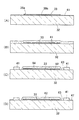
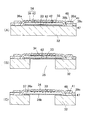
つぎに、音響センサ31のMEMS技術による製造方法を説明する。図4(A)−図4(D)及び図5(A)−図5(C)は、音響センサ31の製造工程を示す概略断面図である。
32 シリコン基板
33 ダイアフラム
34 バックプレート
35 バックチャンバ
37 アンカー
38 アコースティックホール
39 プレート部
40 固定電極膜
41 土台部
45 固定側電極パッド
46 可動側電極パッド
47 密着層
49 梁部カバー領域
50 境界領域
51 土台被覆部
52 平坦部
53 保護膜
61 犠牲層
62 空洞成形部
Claims (13)
- バックチャンバを有する半導体基板と、前記半導体基板の上方に配設された導電性のダイアフラムと、間隙を隔てて前記ダイアフラムを覆うようにして前記半導体基板の上面に固定された絶縁性の固定膜と、前記ダイアフラムと対向する位置において前記固定膜に設けた導電性の固定電極膜と、前記固定電極膜と前記ダイアフラムの間の静電容量の変化を電気信号として外部へ出力するための電極端子とを備えた音響センサであって、
前記半導体基板の上面外周部が前記固定膜と同じ材料からなる保護膜によって覆われていて、前記保護膜の外周が前記半導体基板の上面外周と一致しており、
前記保護膜の外周部は、前記固定膜と異なる材料からなり前記保護膜よりも薄い密着層を介在させて前記半導体基板の表面に固定され、
前記保護膜の内周部は、前記固定膜と異なる材料からなる厚膜層を介在させて前記半導体基板の表面に固定されていることを特徴とする音響センサ。 - 前記電極端子は、前記厚膜層の形成されている領域において前記保護膜に設けられていることを特徴とする、請求項1に記載の音響センサ。
- 前記密着層と前記厚膜層は、同じ材料によって形成されていることを特徴とする、請求項1に記載の音響センサ。
- 前記密着層及び前記厚膜層は、絶縁性材料によって形成されていることを特徴とする、請求項1に記載の音響センサ。
- 前記保護膜と前記固定膜とは連続しており、前記保護膜と前記固定膜との境界領域は、前記半導体基板の上面に密着していることを特徴とする、請求項1に記載の音響センサ。
- バックチャンバを有する半導体基板と、前記半導体基板の上方に配設された導電性のダイアフラムと、間隙を隔てて前記ダイアフラムを覆うようにして前記半導体基板の上面に固定された絶縁性の固定膜と、前記ダイアフラムと対向する位置において前記固定膜に設けた導電性の固定電極膜と、前記固定電極膜と前記ダイアフラムの間の静電容量の変化を電気信号として外部へ出力するための電極端子とを備えた音響センサの製造方法であって、
前記半導体基板の上面に堆積させた犠牲層の内部にダイアフラムを形成する工程と、
前記犠牲層をエッチングして表面が前記固定膜の内面形状をした空間成形部を形成する工程と、
前記空間成形部を形成した後、前記半導体基板の上面外周部の少なくとも一部に、前記固定膜と異なる材料からなり前記保護膜よりも薄い密着層を形成する工程と、
整形された前記犠牲層の上に前記固定膜を形成するとともに、前記密着層を介在させて、かつ、外周が前記半導体基板の上面外周と一致するようにして、前記固定膜と同じ材料からなる保護膜によって前記半導体基板の上面外周部を覆う工程と、
前記半導体基板に前記バックチャンバを形成する工程と、
前記犠牲層をエッチングにより除去して前記ダイアフラムを空間で支持させるとともに、前記ダイアフラムと前記固定膜の内面との間に間隙を形成する工程と、
を有することを特徴とする音響センサの製造方法。 - 前記空間成形部を形成する際、前記犠牲層によって前記空間成形部と分離して前記空間成形部の外側に厚膜層を形成し、ついで、前記厚膜層の外側に前記密着層を形成することを特徴とする、請求項6に記載の音響センサの製造方法。
- 前記密着層と前記厚膜層は、同じ材料によって形成されていることを特徴とする、請求項7に記載の音響センサの製造方法。
- 前記密着層及び前記厚膜層は、絶縁性材料によって形成されていることを特徴とする、請求項7に記載の音響センサの製造方法。
- 前記密着層の厚さは、前記固定膜と前記固定電極膜からなるバックプレートの内面と前記ダイアフラムとの間の間隔よりも小さいことを特徴とする、請求項7に記載の音響センサの製造方法。
- 前記厚膜層の厚さは、前記固定膜と前記固定電極膜からなるバックプレートの内面と前記ダイアフラムとの間の間隔よりも大きいことを特徴とする、請求項7に記載の音響センサの製造方法。
- 前記厚膜層の厚さは、前記固定膜と前記固定電極膜からなるバックプレートの内面と前記ダイアフラムとの間の間隔と、前記半導体基板の上面と前記ダイアフラムとの間の間隔との和の距離に等しいことを特徴とする、請求項7に記載の音響センサの製造方法。
- 前記保護膜と前記固定膜を連続させて同時に形成するとともに、前記保護膜と前記固定膜との境界領域を前記半導体基板の上面に密着させることを特徴とする、請求項7に記載の音響センサの製造方法。
Priority Applications (5)
| Application Number | Priority Date | Filing Date | Title |
|---|---|---|---|
| JP2010109164A JP5454345B2 (ja) | 2010-05-11 | 2010-05-11 | 音響センサ及びその製造方法 |
| KR1020110031730A KR101201642B1 (ko) | 2010-05-11 | 2011-04-06 | 음향 센서 및 그 제조 방법 |
| EP11161590.2A EP2386521B1 (en) | 2010-05-11 | 2011-04-08 | Acoustic sensor having protective film and method of manufacturing the same |
| US13/104,387 US9199837B2 (en) | 2010-05-11 | 2011-05-10 | Acoustic sensor and method of manufacturing the same |
| CN201110119075.8A CN102244829B (zh) | 2010-05-11 | 2011-05-10 | 声音传感器及其制造方法 |
Applications Claiming Priority (1)
| Application Number | Priority Date | Filing Date | Title |
|---|---|---|---|
| JP2010109164A JP5454345B2 (ja) | 2010-05-11 | 2010-05-11 | 音響センサ及びその製造方法 |
Publications (2)
| Publication Number | Publication Date |
|---|---|
| JP2011239197A JP2011239197A (ja) | 2011-11-24 |
| JP5454345B2 true JP5454345B2 (ja) | 2014-03-26 |
Family
ID=44357174
Family Applications (1)
| Application Number | Title | Priority Date | Filing Date |
|---|---|---|---|
| JP2010109164A Expired - Fee Related JP5454345B2 (ja) | 2010-05-11 | 2010-05-11 | 音響センサ及びその製造方法 |
Country Status (5)
| Country | Link |
|---|---|
| US (1) | US9199837B2 (ja) |
| EP (1) | EP2386521B1 (ja) |
| JP (1) | JP5454345B2 (ja) |
| KR (1) | KR101201642B1 (ja) |
| CN (1) | CN102244829B (ja) |
Families Citing this family (20)
| Publication number | Priority date | Publication date | Assignee | Title |
|---|---|---|---|---|
| JP5177309B1 (ja) | 2012-01-31 | 2013-04-03 | オムロン株式会社 | 静電容量型センサ |
| DE102013201795A1 (de) * | 2013-02-05 | 2014-08-07 | Robert Bosch Gmbh | Mikromechanisches Bauelement mit einer Membranstruktur |
| US9338559B2 (en) * | 2013-04-16 | 2016-05-10 | Invensense, Inc. | Microphone system with a stop member |
| DE102013213717A1 (de) * | 2013-07-12 | 2015-01-15 | Robert Bosch Gmbh | MEMS-Bauelement mit einer Mikrofonstruktur und Verfahren zu dessen Herstellung |
| KR20150049193A (ko) * | 2013-10-29 | 2015-05-08 | 한국전자통신연구원 | 음향 센서 |
| JP6252767B2 (ja) * | 2014-03-14 | 2017-12-27 | オムロン株式会社 | 静電容量型トランスデューサ |
| CN105203235B (zh) * | 2014-06-19 | 2018-04-13 | 中芯国际集成电路制造(上海)有限公司 | 一种mems压力传感器的制造方法和电子装置 |
| CN105502277A (zh) * | 2014-09-24 | 2016-04-20 | 中芯国际集成电路制造(上海)有限公司 | 一种mems麦克风及其制作方法和电子装置 |
| DE102015204793A1 (de) * | 2015-03-17 | 2016-09-22 | Robert Bosch Gmbh | Vorrichtung und Verfahren zum Bearbeiten einer Zielzellen enthaltenden Probe biologischen Materials |
| KR101688954B1 (ko) * | 2016-01-15 | 2016-12-22 | (주)글로벌센싱테크놀로지 | 멤브레인 지지 구조가 개선된 마이크로폰 및 마이크로폰 제조 방법 |
| JP6809008B2 (ja) * | 2016-07-08 | 2021-01-06 | オムロン株式会社 | Mems構造及び、mems構造を有する静電容量型センサ、圧電型センサ、音響センサ |
| KR102371228B1 (ko) * | 2016-11-24 | 2022-03-04 | 현대자동차 주식회사 | 마이크로폰 및 이의 제조방법 |
| CN108609573A (zh) * | 2016-12-12 | 2018-10-02 | 中芯国际集成电路制造(上海)有限公司 | 一种mems器件及其制备方法、电子装置 |
| CN108346566B (zh) | 2017-01-22 | 2021-02-09 | 中芯国际集成电路制造(上海)有限公司 | 半导体装置及其制造方法 |
| KR102212575B1 (ko) * | 2017-02-02 | 2021-02-04 | 현대자동차 주식회사 | 마이크로폰 및 그 제조 방법 |
| KR102322258B1 (ko) * | 2017-05-19 | 2021-11-04 | 현대자동차 주식회사 | 마이크로폰 및 그 제조 방법 |
| IT201800004758A1 (it) * | 2018-04-20 | 2019-10-20 | Trasduttore acustico mems piezoelettrico e relativo procedimento di fabbricazione | |
| US11239408B2 (en) * | 2018-09-04 | 2022-02-01 | Kathirgamasundaram Sooriakumar | Acoustic transducer and related fabrication and packaging techniques |
| CN115885522A (zh) * | 2020-05-05 | 2023-03-31 | Tdk电子股份有限公司 | 具有隔膜沟槽加强件的微机电麦克风和制造方法 |
| US11312616B1 (en) * | 2020-10-27 | 2022-04-26 | Solid State System Co., Ltd. | Structure of micro-electro-mechanical-system microphone and method for fabricating the same |
Family Cites Families (41)
| Publication number | Priority date | Publication date | Assignee | Title |
|---|---|---|---|---|
| JP3440037B2 (ja) * | 1999-09-16 | 2003-08-25 | 三洋電機株式会社 | 半導体装置、半導体エレクトレットコンデンサマイクロホンおよび半導体エレクトレットコンデンサマイクロホンの製造方法。 |
| US6535460B2 (en) * | 2000-08-11 | 2003-03-18 | Knowles Electronics, Llc | Miniature broadband acoustic transducer |
| US6936837B2 (en) * | 2001-05-11 | 2005-08-30 | Ube Industries, Ltd. | Film bulk acoustic resonator |
| WO2003047307A2 (en) * | 2001-11-27 | 2003-06-05 | Corporation For National Research Initiatives | A miniature condenser microphone and fabrication method therefor |
| US6677176B2 (en) * | 2002-01-18 | 2004-01-13 | The Hong Kong University Of Science And Technology | Method of manufacturing an integrated electronic microphone having a floating gate electrode |
| US6928178B2 (en) * | 2002-12-17 | 2005-08-09 | Taiwan Carol Electronics Co., Ltd. | Condenser microphone and method for making the same |
| US7134343B2 (en) * | 2003-07-25 | 2006-11-14 | Kabushiki Kaisha Toshiba | Opto-acoustoelectric device and methods for analyzing mechanical vibration and sound |
| WO2005050680A1 (ja) * | 2003-11-20 | 2005-06-02 | Matsushita Electric Industrial Co., Ltd. | エレクトレット及びエレクトレットコンデンサー |
| JP4497321B2 (ja) * | 2003-12-26 | 2010-07-07 | 日本電気株式会社 | 圧電アクチュエータ |
| JP4036866B2 (ja) * | 2004-07-30 | 2008-01-23 | 三洋電機株式会社 | 音響センサ |
| JP2006121465A (ja) * | 2004-10-22 | 2006-05-11 | Sanyo Electric Co Ltd | 音響センサ及び音響センサの製造方法 |
| JP4539450B2 (ja) * | 2004-11-04 | 2010-09-08 | オムロン株式会社 | 容量型振動センサ及びその製造方法 |
| US7849648B2 (en) * | 2004-12-30 | 2010-12-14 | United States Gypsum Company | Non-combustible reinforced cementitious lightweight panels and metal frame system for flooring |
| US7373835B2 (en) * | 2005-01-31 | 2008-05-20 | Sanyo Electric Industries, Ltd. | Semiconductor sensor |
| US20060291674A1 (en) * | 2005-06-14 | 2006-12-28 | Merry Electronics Co. Ltd. | Method of making silicon-based miniaturized microphones |
| JP2007097116A (ja) * | 2005-08-29 | 2007-04-12 | Sanyo Electric Co Ltd | センサ |
| EP1922898A1 (en) * | 2005-09-09 | 2008-05-21 | Yamaha Corporation | Capacitor microphone |
| US8126167B2 (en) * | 2006-03-29 | 2012-02-28 | Yamaha Corporation | Condenser microphone |
| JP4742972B2 (ja) * | 2006-04-27 | 2011-08-10 | オムロン株式会社 | マイクロフォンの製造方法 |
| KR101416512B1 (ko) * | 2006-05-18 | 2014-07-08 | 가부시키가이샤 한도오따이 에네루기 켄큐쇼 | 미소 구조체, 마이크로머신, 미소 구조체 및 마이크로머신의 제조방법 |
| US8081783B2 (en) * | 2006-06-20 | 2011-12-20 | Industrial Technology Research Institute | Miniature acoustic transducer |
| TW200826717A (en) * | 2006-10-16 | 2008-06-16 | Yamaha Corp | Electrostatic pressure transducer and manufacturing method therefor |
| US8121315B2 (en) * | 2007-03-21 | 2012-02-21 | Goer Tek Inc. | Condenser microphone chip |
| JP5034692B2 (ja) * | 2007-06-04 | 2012-09-26 | オムロン株式会社 | 音響センサ |
| JP5029147B2 (ja) * | 2007-06-04 | 2012-09-19 | オムロン株式会社 | 音響センサ |
| JP2009038732A (ja) * | 2007-08-03 | 2009-02-19 | Panasonic Corp | 電子部品とその製造方法及び該電子部品を備える電子装置 |
| JP2009089097A (ja) * | 2007-09-28 | 2009-04-23 | Yamaha Corp | 振動トランスデューサ |
| US20090136064A1 (en) * | 2007-09-28 | 2009-05-28 | Yamaha Corporation | Vibration transducer and manufacturing method therefor |
| JP5070026B2 (ja) * | 2007-12-17 | 2012-11-07 | 新日本無線株式会社 | コンデンサマイクロホン及びその製造方法 |
| US7888754B2 (en) * | 2007-12-28 | 2011-02-15 | Yamaha Corporation | MEMS transducer |
| CN101785325B (zh) * | 2008-02-20 | 2013-07-17 | 欧姆龙株式会社 | 静电电容式振动传感器 |
| JP4392466B1 (ja) * | 2008-06-24 | 2010-01-06 | パナソニック株式会社 | Memsデバイス、memsデバイスモジュール及び音響トランスデューサ |
| JP5332373B2 (ja) * | 2008-07-25 | 2013-11-06 | オムロン株式会社 | 静電容量型振動センサ |
| JP4419103B1 (ja) * | 2008-08-27 | 2010-02-24 | オムロン株式会社 | 静電容量型振動センサ |
| JP2010074523A (ja) | 2008-09-18 | 2010-04-02 | Rohm Co Ltd | 犠牲層のエッチング方法、memsデバイスの製造方法およびmemsデバイス |
| US20100065930A1 (en) * | 2008-09-18 | 2010-03-18 | Rohm Co., Ltd. | Method of etching sacrificial layer, method of manufacturing MEMS device, MEMS device and MEMS sensor |
| JP2010098518A (ja) | 2008-10-16 | 2010-04-30 | Rohm Co Ltd | Memsセンサの製造方法およびmemsセンサ |
| JP2010103701A (ja) * | 2008-10-22 | 2010-05-06 | Rohm Co Ltd | Memsセンサ |
| JP4947168B2 (ja) * | 2010-02-24 | 2012-06-06 | オムロン株式会社 | 音響センサ |
| JP5402823B2 (ja) * | 2010-05-13 | 2014-01-29 | オムロン株式会社 | 音響センサ |
| JP4947220B2 (ja) * | 2010-05-13 | 2012-06-06 | オムロン株式会社 | 音響センサ及びマイクロフォン |
-
2010
- 2010-05-11 JP JP2010109164A patent/JP5454345B2/ja not_active Expired - Fee Related
-
2011
- 2011-04-06 KR KR1020110031730A patent/KR101201642B1/ko active IP Right Grant
- 2011-04-08 EP EP11161590.2A patent/EP2386521B1/en active Active
- 2011-05-10 CN CN201110119075.8A patent/CN102244829B/zh active Active
- 2011-05-10 US US13/104,387 patent/US9199837B2/en active Active
Also Published As
| Publication number | Publication date |
|---|---|
| US20110278683A1 (en) | 2011-11-17 |
| CN102244829A (zh) | 2011-11-16 |
| KR20110124702A (ko) | 2011-11-17 |
| JP2011239197A (ja) | 2011-11-24 |
| KR101201642B1 (ko) | 2012-11-14 |
| EP2386521A3 (en) | 2014-01-15 |
| EP2386521A2 (en) | 2011-11-16 |
| US9199837B2 (en) | 2015-12-01 |
| CN102244829B (zh) | 2014-10-22 |
| EP2386521B1 (en) | 2018-06-13 |
Similar Documents
| Publication | Publication Date | Title |
|---|---|---|
| JP5454345B2 (ja) | 音響センサ及びその製造方法 | |
| JP5083369B2 (ja) | 音響センサ及びその製造方法 | |
| US8803257B2 (en) | Capacitive vibration sensor | |
| US8542851B2 (en) | Acoustic sensor and microphone | |
| JP6127600B2 (ja) | 静電容量型センサ、音響センサ及びマイクロフォン | |
| US8098870B2 (en) | Silicon microphone | |
| KR101740113B1 (ko) | 주변압에서의 변화 및 압력파를 센싱하기 위한 mems 센서 구조체 | |
| WO2009045170A1 (en) | Silicon microphone with enhanced impact proof structure using bonding wires | |
| JP2014090514A (ja) | マイクロメカニカルマイクロフォン構造体を有する素子、および、マイクロメカニカルマイクロフォン構造体を有する素子の製造方法 | |
| JP5721452B2 (ja) | 静電容量型memsセンサ | |
| JP2010238921A (ja) | Memsセンサ | |
| JP2012028900A (ja) | コンデンサマイクロホン | |
| JP2009081624A (ja) | 半導体センサ装置 | |
| JP6582273B2 (ja) | Mems素子の製造方法 | |
| JP2009055490A (ja) | マイクロホン装置 | |
| JP2007311392A (ja) | 電子装置 | |
| JP2009115499A (ja) | 物理量センサ及びその製造方法 |
Legal Events
| Date | Code | Title | Description |
|---|---|---|---|
| A621 | Written request for application examination |
Free format text: JAPANESE INTERMEDIATE CODE: A621 Effective date: 20130307 |
|
| A977 | Report on retrieval |
Free format text: JAPANESE INTERMEDIATE CODE: A971007 Effective date: 20130920 |
|
| A131 | Notification of reasons for refusal |
Free format text: JAPANESE INTERMEDIATE CODE: A131 Effective date: 20130925 |
|
| A521 | Request for written amendment filed |
Free format text: JAPANESE INTERMEDIATE CODE: A523 Effective date: 20131120 |
|
| TRDD | Decision of grant or rejection written | ||
| A01 | Written decision to grant a patent or to grant a registration (utility model) |
Free format text: JAPANESE INTERMEDIATE CODE: A01 Effective date: 20131210 |
|
| A61 | First payment of annual fees (during grant procedure) |
Free format text: JAPANESE INTERMEDIATE CODE: A61 Effective date: 20131223 |
|
| R150 | Certificate of patent or registration of utility model |
Ref document number: 5454345 Country of ref document: JP Free format text: JAPANESE INTERMEDIATE CODE: R150 Free format text: JAPANESE INTERMEDIATE CODE: R150 |
|
| S111 | Request for change of ownership or part of ownership |
Free format text: JAPANESE INTERMEDIATE CODE: R313111 |
|
| R350 | Written notification of registration of transfer |
Free format text: JAPANESE INTERMEDIATE CODE: R350 |
|
| LAPS | Cancellation because of no payment of annual fees |