JP5394048B2 - 蒸着用基板 - Google Patents
蒸着用基板 Download PDFInfo
- Publication number
- JP5394048B2 JP5394048B2 JP2008302769A JP2008302769A JP5394048B2 JP 5394048 B2 JP5394048 B2 JP 5394048B2 JP 2008302769 A JP2008302769 A JP 2008302769A JP 2008302769 A JP2008302769 A JP 2008302769A JP 5394048 B2 JP5394048 B2 JP 5394048B2
- Authority
- JP
- Japan
- Prior art keywords
- layer
- substrate
- light
- deposition
- support substrate
- Prior art date
- Legal status (The legal status is an assumption and is not a legal conclusion. Google has not performed a legal analysis and makes no representation as to the accuracy of the status listed.)
- Expired - Fee Related
Links
Images




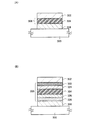


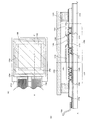


Classifications
-
- B—PERFORMING OPERATIONS; TRANSPORTING
- B32—LAYERED PRODUCTS
- B32B—LAYERED PRODUCTS, i.e. PRODUCTS BUILT-UP OF STRATA OF FLAT OR NON-FLAT, e.g. CELLULAR OR HONEYCOMB, FORM
- B32B3/00—Layered products comprising a layer with external or internal discontinuities or unevennesses, or a layer of non-planar shape; Layered products comprising a layer having particular features of form
- B32B3/10—Layered products comprising a layer with external or internal discontinuities or unevennesses, or a layer of non-planar shape; Layered products comprising a layer having particular features of form characterised by a discontinuous layer, i.e. formed of separate pieces of material
-
- H—ELECTRICITY
- H05—ELECTRIC TECHNIQUES NOT OTHERWISE PROVIDED FOR
- H05B—ELECTRIC HEATING; ELECTRIC LIGHT SOURCES NOT OTHERWISE PROVIDED FOR; CIRCUIT ARRANGEMENTS FOR ELECTRIC LIGHT SOURCES, IN GENERAL
- H05B33/00—Electroluminescent light sources
- H05B33/10—Apparatus or processes specially adapted to the manufacture of electroluminescent light sources
-
- B—PERFORMING OPERATIONS; TRANSPORTING
- B32—LAYERED PRODUCTS
- B32B—LAYERED PRODUCTS, i.e. PRODUCTS BUILT-UP OF STRATA OF FLAT OR NON-FLAT, e.g. CELLULAR OR HONEYCOMB, FORM
- B32B15/00—Layered products comprising a layer of metal
- B32B15/04—Layered products comprising a layer of metal comprising metal as the main or only constituent of a layer, which is next to another layer of the same or of a different material
- B32B15/043—Layered products comprising a layer of metal comprising metal as the main or only constituent of a layer, which is next to another layer of the same or of a different material of metal
-
- B—PERFORMING OPERATIONS; TRANSPORTING
- B32—LAYERED PRODUCTS
- B32B—LAYERED PRODUCTS, i.e. PRODUCTS BUILT-UP OF STRATA OF FLAT OR NON-FLAT, e.g. CELLULAR OR HONEYCOMB, FORM
- B32B15/00—Layered products comprising a layer of metal
- B32B15/04—Layered products comprising a layer of metal comprising metal as the main or only constituent of a layer, which is next to another layer of the same or of a different material
- B32B15/08—Layered products comprising a layer of metal comprising metal as the main or only constituent of a layer, which is next to another layer of the same or of a different material of synthetic resin
-
- B—PERFORMING OPERATIONS; TRANSPORTING
- B32—LAYERED PRODUCTS
- B32B—LAYERED PRODUCTS, i.e. PRODUCTS BUILT-UP OF STRATA OF FLAT OR NON-FLAT, e.g. CELLULAR OR HONEYCOMB, FORM
- B32B27/00—Layered products comprising a layer of synthetic resin
- B32B27/28—Layered products comprising a layer of synthetic resin comprising synthetic resins not wholly covered by any one of the sub-groups B32B27/30 - B32B27/42
- B32B27/281—Layered products comprising a layer of synthetic resin comprising synthetic resins not wholly covered by any one of the sub-groups B32B27/30 - B32B27/42 comprising polyimides
-
- B—PERFORMING OPERATIONS; TRANSPORTING
- B32—LAYERED PRODUCTS
- B32B—LAYERED PRODUCTS, i.e. PRODUCTS BUILT-UP OF STRATA OF FLAT OR NON-FLAT, e.g. CELLULAR OR HONEYCOMB, FORM
- B32B27/00—Layered products comprising a layer of synthetic resin
- B32B27/30—Layered products comprising a layer of synthetic resin comprising vinyl (co)polymers; comprising acrylic (co)polymers
- B32B27/304—Layered products comprising a layer of synthetic resin comprising vinyl (co)polymers; comprising acrylic (co)polymers comprising vinyl halide (co)polymers, e.g. PVC, PVDC, PVF, PVDF
-
- B—PERFORMING OPERATIONS; TRANSPORTING
- B32—LAYERED PRODUCTS
- B32B—LAYERED PRODUCTS, i.e. PRODUCTS BUILT-UP OF STRATA OF FLAT OR NON-FLAT, e.g. CELLULAR OR HONEYCOMB, FORM
- B32B27/00—Layered products comprising a layer of synthetic resin
- B32B27/30—Layered products comprising a layer of synthetic resin comprising vinyl (co)polymers; comprising acrylic (co)polymers
- B32B27/308—Layered products comprising a layer of synthetic resin comprising vinyl (co)polymers; comprising acrylic (co)polymers comprising acrylic (co)polymers
-
- B—PERFORMING OPERATIONS; TRANSPORTING
- B32—LAYERED PRODUCTS
- B32B—LAYERED PRODUCTS, i.e. PRODUCTS BUILT-UP OF STRATA OF FLAT OR NON-FLAT, e.g. CELLULAR OR HONEYCOMB, FORM
- B32B27/00—Layered products comprising a layer of synthetic resin
- B32B27/34—Layered products comprising a layer of synthetic resin comprising polyamides
-
- B—PERFORMING OPERATIONS; TRANSPORTING
- B32—LAYERED PRODUCTS
- B32B—LAYERED PRODUCTS, i.e. PRODUCTS BUILT-UP OF STRATA OF FLAT OR NON-FLAT, e.g. CELLULAR OR HONEYCOMB, FORM
- B32B27/00—Layered products comprising a layer of synthetic resin
- B32B27/36—Layered products comprising a layer of synthetic resin comprising polyesters
-
- B—PERFORMING OPERATIONS; TRANSPORTING
- B32—LAYERED PRODUCTS
- B32B—LAYERED PRODUCTS, i.e. PRODUCTS BUILT-UP OF STRATA OF FLAT OR NON-FLAT, e.g. CELLULAR OR HONEYCOMB, FORM
- B32B3/00—Layered products comprising a layer with external or internal discontinuities or unevennesses, or a layer of non-planar shape; Layered products comprising a layer having particular features of form
- B32B3/10—Layered products comprising a layer with external or internal discontinuities or unevennesses, or a layer of non-planar shape; Layered products comprising a layer having particular features of form characterised by a discontinuous layer, i.e. formed of separate pieces of material
- B32B3/12—Layered products comprising a layer with external or internal discontinuities or unevennesses, or a layer of non-planar shape; Layered products comprising a layer having particular features of form characterised by a discontinuous layer, i.e. formed of separate pieces of material characterised by a layer of regularly- arranged cells, e.g. a honeycomb structure
-
- B—PERFORMING OPERATIONS; TRANSPORTING
- B32—LAYERED PRODUCTS
- B32B—LAYERED PRODUCTS, i.e. PRODUCTS BUILT-UP OF STRATA OF FLAT OR NON-FLAT, e.g. CELLULAR OR HONEYCOMB, FORM
- B32B3/00—Layered products comprising a layer with external or internal discontinuities or unevennesses, or a layer of non-planar shape; Layered products comprising a layer having particular features of form
- B32B3/26—Layered products comprising a layer with external or internal discontinuities or unevennesses, or a layer of non-planar shape; Layered products comprising a layer having particular features of form characterised by a particular shape of the outline of the cross-section of a continuous layer; characterised by a layer with cavities or internal voids ; characterised by an apertured layer
- B32B3/30—Layered products comprising a layer with external or internal discontinuities or unevennesses, or a layer of non-planar shape; Layered products comprising a layer having particular features of form characterised by a particular shape of the outline of the cross-section of a continuous layer; characterised by a layer with cavities or internal voids ; characterised by an apertured layer characterised by a layer formed with recesses or projections, e.g. hollows, grooves, protuberances, ribs
-
- B—PERFORMING OPERATIONS; TRANSPORTING
- B32—LAYERED PRODUCTS
- B32B—LAYERED PRODUCTS, i.e. PRODUCTS BUILT-UP OF STRATA OF FLAT OR NON-FLAT, e.g. CELLULAR OR HONEYCOMB, FORM
- B32B7/00—Layered products characterised by the relation between layers; Layered products characterised by the relative orientation of features between layers, or by the relative values of a measurable parameter between layers, i.e. products comprising layers having different physical, chemical or physicochemical properties; Layered products characterised by the interconnection of layers
- B32B7/04—Interconnection of layers
- B32B7/12—Interconnection of layers using interposed adhesives or interposed materials with bonding properties
-
- C—CHEMISTRY; METALLURGY
- C23—COATING METALLIC MATERIAL; COATING MATERIAL WITH METALLIC MATERIAL; CHEMICAL SURFACE TREATMENT; DIFFUSION TREATMENT OF METALLIC MATERIAL; COATING BY VACUUM EVAPORATION, BY SPUTTERING, BY ION IMPLANTATION OR BY CHEMICAL VAPOUR DEPOSITION, IN GENERAL; INHIBITING CORROSION OF METALLIC MATERIAL OR INCRUSTATION IN GENERAL
- C23C—COATING METALLIC MATERIAL; COATING MATERIAL WITH METALLIC MATERIAL; SURFACE TREATMENT OF METALLIC MATERIAL BY DIFFUSION INTO THE SURFACE, BY CHEMICAL CONVERSION OR SUBSTITUTION; COATING BY VACUUM EVAPORATION, BY SPUTTERING, BY ION IMPLANTATION OR BY CHEMICAL VAPOUR DEPOSITION, IN GENERAL
- C23C14/00—Coating by vacuum evaporation, by sputtering or by ion implantation of the coating forming material
- C23C14/04—Coating on selected surface areas, e.g. using masks
- C23C14/048—Coating on selected surface areas, e.g. using masks using irradiation by energy or particles
-
- H—ELECTRICITY
- H10—SEMICONDUCTOR DEVICES; ELECTRIC SOLID-STATE DEVICES NOT OTHERWISE PROVIDED FOR
- H10K—ORGANIC ELECTRIC SOLID-STATE DEVICES
- H10K71/00—Manufacture or treatment specially adapted for the organic devices covered by this subclass
-
- H—ELECTRICITY
- H10—SEMICONDUCTOR DEVICES; ELECTRIC SOLID-STATE DEVICES NOT OTHERWISE PROVIDED FOR
- H10K—ORGANIC ELECTRIC SOLID-STATE DEVICES
- H10K71/00—Manufacture or treatment specially adapted for the organic devices covered by this subclass
- H10K71/10—Deposition of organic active material
- H10K71/18—Deposition of organic active material using non-liquid printing techniques, e.g. thermal transfer printing from a donor sheet
-
- B—PERFORMING OPERATIONS; TRANSPORTING
- B32—LAYERED PRODUCTS
- B32B—LAYERED PRODUCTS, i.e. PRODUCTS BUILT-UP OF STRATA OF FLAT OR NON-FLAT, e.g. CELLULAR OR HONEYCOMB, FORM
- B32B2262/00—Composition or structural features of fibres which form a fibrous or filamentary layer or are present as additives
- B32B2262/10—Inorganic fibres
- B32B2262/101—Glass fibres
-
- B—PERFORMING OPERATIONS; TRANSPORTING
- B32—LAYERED PRODUCTS
- B32B—LAYERED PRODUCTS, i.e. PRODUCTS BUILT-UP OF STRATA OF FLAT OR NON-FLAT, e.g. CELLULAR OR HONEYCOMB, FORM
- B32B2307/00—Properties of the layers or laminate
- B32B2307/20—Properties of the layers or laminate having particular electrical or magnetic properties, e.g. piezoelectric
- B32B2307/206—Insulating
-
- B—PERFORMING OPERATIONS; TRANSPORTING
- B32—LAYERED PRODUCTS
- B32B—LAYERED PRODUCTS, i.e. PRODUCTS BUILT-UP OF STRATA OF FLAT OR NON-FLAT, e.g. CELLULAR OR HONEYCOMB, FORM
- B32B2307/00—Properties of the layers or laminate
- B32B2307/40—Properties of the layers or laminate having particular optical properties
- B32B2307/416—Reflective
-
- B—PERFORMING OPERATIONS; TRANSPORTING
- B32—LAYERED PRODUCTS
- B32B—LAYERED PRODUCTS, i.e. PRODUCTS BUILT-UP OF STRATA OF FLAT OR NON-FLAT, e.g. CELLULAR OR HONEYCOMB, FORM
- B32B2457/00—Electrical equipment
- B32B2457/20—Displays, e.g. liquid crystal displays, plasma displays
-
- Y—GENERAL TAGGING OF NEW TECHNOLOGICAL DEVELOPMENTS; GENERAL TAGGING OF CROSS-SECTIONAL TECHNOLOGIES SPANNING OVER SEVERAL SECTIONS OF THE IPC; TECHNICAL SUBJECTS COVERED BY FORMER USPC CROSS-REFERENCE ART COLLECTIONS [XRACs] AND DIGESTS
- Y10—TECHNICAL SUBJECTS COVERED BY FORMER USPC
- Y10T—TECHNICAL SUBJECTS COVERED BY FORMER US CLASSIFICATION
- Y10T428/00—Stock material or miscellaneous articles
- Y10T428/24—Structurally defined web or sheet [e.g., overall dimension, etc.]
- Y10T428/24273—Structurally defined web or sheet [e.g., overall dimension, etc.] including aperture
- Y10T428/24322—Composite web or sheet
- Y10T428/24331—Composite web or sheet including nonapertured component
- Y10T428/24339—Keyed
Landscapes
- Chemical & Material Sciences (AREA)
- Engineering & Computer Science (AREA)
- Manufacturing & Machinery (AREA)
- Health & Medical Sciences (AREA)
- Toxicology (AREA)
- Chemical Kinetics & Catalysis (AREA)
- Materials Engineering (AREA)
- Mechanical Engineering (AREA)
- Metallurgy (AREA)
- Organic Chemistry (AREA)
- Electroluminescent Light Sources (AREA)
Priority Applications (1)
| Application Number | Priority Date | Filing Date | Title |
|---|---|---|---|
| JP2008302769A JP5394048B2 (ja) | 2007-11-29 | 2008-11-27 | 蒸着用基板 |
Applications Claiming Priority (3)
| Application Number | Priority Date | Filing Date | Title |
|---|---|---|---|
| JP2007308606 | 2007-11-29 | ||
| JP2007308606 | 2007-11-29 | ||
| JP2008302769A JP5394048B2 (ja) | 2007-11-29 | 2008-11-27 | 蒸着用基板 |
Publications (3)
| Publication Number | Publication Date |
|---|---|
| JP2009152187A JP2009152187A (ja) | 2009-07-09 |
| JP2009152187A5 JP2009152187A5 (enExample) | 2011-10-20 |
| JP5394048B2 true JP5394048B2 (ja) | 2014-01-22 |
Family
ID=40676005
Family Applications (1)
| Application Number | Title | Priority Date | Filing Date |
|---|---|---|---|
| JP2008302769A Expired - Fee Related JP5394048B2 (ja) | 2007-11-29 | 2008-11-27 | 蒸着用基板 |
Country Status (3)
| Country | Link |
|---|---|
| US (1) | US8425974B2 (enExample) |
| JP (1) | JP5394048B2 (enExample) |
| KR (1) | KR20090056920A (enExample) |
Families Citing this family (27)
| Publication number | Priority date | Publication date | Assignee | Title |
|---|---|---|---|---|
| KR101689519B1 (ko) * | 2007-12-26 | 2016-12-26 | 가부시키가이샤 한도오따이 에네루기 켄큐쇼 | 증착용 기판, 증착용 기판의 제조방법, 및 발광장치의 제조방법 |
| US8080811B2 (en) | 2007-12-28 | 2011-12-20 | Semiconductor Energy Laboratory Co., Ltd. | Method for manufacturing evaporation donor substrate and light-emitting device |
| WO2009099002A1 (en) | 2008-02-04 | 2009-08-13 | Semiconductor Energy Laboratory Co., Ltd. | Deposition method and method for manufacturing light-emitting device |
| JP2009187810A (ja) * | 2008-02-07 | 2009-08-20 | Seiko Epson Corp | 発光装置の製造方法 |
| JP5416987B2 (ja) * | 2008-02-29 | 2014-02-12 | 株式会社半導体エネルギー研究所 | 成膜方法及び発光装置の作製方法 |
| WO2009107548A1 (en) * | 2008-02-29 | 2009-09-03 | Semiconductor Energy Laboratory Co., Ltd. | Deposition method and manufacturing method of light-emitting device |
| US8182863B2 (en) * | 2008-03-17 | 2012-05-22 | Semiconductor Energy Laboratory Co., Ltd. | Deposition method and manufacturing method of light-emitting device |
| JP5244680B2 (ja) * | 2008-04-14 | 2013-07-24 | 株式会社半導体エネルギー研究所 | 発光装置の作製方法 |
| KR101629637B1 (ko) * | 2008-05-29 | 2016-06-13 | 가부시키가이샤 한도오따이 에네루기 켄큐쇼 | 성막방법 및 발광장치의 제조방법 |
| JP4992975B2 (ja) * | 2008-06-16 | 2012-08-08 | 東レ株式会社 | パターニング方法およびこれを用いたデバイスの製造方法ならびにデバイス |
| WO2010016331A1 (ja) * | 2008-08-05 | 2010-02-11 | 東レ株式会社 | デバイスの製造方法 |
| US8486736B2 (en) | 2008-10-20 | 2013-07-16 | Semiconductor Energy Laboratory Co., Ltd. | Method for manufacturing light-emitting device |
| JP5258666B2 (ja) * | 2009-04-22 | 2013-08-07 | 株式会社半導体エネルギー研究所 | 発光装置の作製方法および成膜用基板 |
| KR20120042144A (ko) * | 2010-10-22 | 2012-05-03 | 삼성모바일디스플레이주식회사 | 레이저 열전사용 마스크, 이를 포함하는 레이저 조사 장치 및 이를 이용한 유기 발광 소자 제조 방법 |
| WO2013184219A1 (en) * | 2012-03-30 | 2013-12-12 | The Trustees Of Columbia University In The City Of New York | Systems and methods for patterning samples |
| EP2660352A1 (en) * | 2012-05-02 | 2013-11-06 | Nederlandse Organisatie voor toegepast -natuurwetenschappelijk onderzoek TNO | Donor sheet and method for light induced forward transfer manufacturing |
| US9494792B2 (en) | 2013-07-30 | 2016-11-15 | Global Oled Technology Llc | Local seal for encapsulation of electro-optical element on a flexible substrate |
| US9287522B2 (en) * | 2013-07-30 | 2016-03-15 | Global Oled Technology Llc | Local seal for encapsulation of electro-optical element on a flexible substrate |
| US9385342B2 (en) | 2013-07-30 | 2016-07-05 | Global Oled Technology Llc | Local seal for encapsulation of electro-optical element on a flexible substrate |
| KR20150056112A (ko) * | 2013-11-14 | 2015-05-26 | 삼성디스플레이 주식회사 | 막 형성용 마스크, 이를 이용한 막 형성 방법 및 유기 발광 표시 장치의 제조 방법 |
| KR20150109013A (ko) * | 2014-03-18 | 2015-10-01 | 삼성디스플레이 주식회사 | 유기막 패턴 형성용 마스크, 이를 이용한 유기막 패턴 형성 방법 및 유기 발광 표시 장치의 제조 방법 |
| DE102014108925A1 (de) * | 2014-06-25 | 2015-12-31 | Von Ardenne Gmbh | Substratbeschichtungseinrichtung und Bedampfungsverfahren |
| KR102325208B1 (ko) * | 2014-08-12 | 2021-11-12 | 삼성디스플레이 주식회사 | 도너마스크, 이를 이용한 유기발광 디스플레이 장치 제조방법 및 유기발광 디스플레이 장치 |
| DE102016124646A1 (de) * | 2016-12-16 | 2018-06-21 | Osram Opto Semiconductors Gmbh | Verfahren zur Herstellung eines Halbleiterbauelements |
| KR102030236B1 (ko) * | 2017-06-16 | 2019-10-08 | 주식회사 야스 | Fmm 없이 컬러 화소를 형성하는 방법 및 장치 |
| KR101985086B1 (ko) * | 2017-08-02 | 2019-06-03 | 주식회사 야스 | Fmm이 없는 재료절감형 컬러 화소 형성 시스템 |
| EP4037442A1 (en) * | 2021-02-01 | 2022-08-03 | Nederlandse Organisatie Voor Toegepast- Natuurwetenschappelijk Onderzoek Tno | Donor plate, deposition device and deposition method |
Family Cites Families (32)
| Publication number | Priority date | Publication date | Assignee | Title |
|---|---|---|---|---|
| US4752455A (en) * | 1986-05-27 | 1988-06-21 | Kms Fusion, Inc. | Pulsed laser microfabrication |
| JP3801730B2 (ja) | 1997-05-09 | 2006-07-26 | 株式会社半導体エネルギー研究所 | プラズマcvd装置及びそれを用いた薄膜形成方法 |
| US5937272A (en) | 1997-06-06 | 1999-08-10 | Eastman Kodak Company | Patterned organic layers in a full-color organic electroluminescent display array on a thin film transistor array substrate |
| US5851709A (en) | 1997-10-31 | 1998-12-22 | Eastman Kodak Company | Method for selective transfer of a color organic layer |
| US6165543A (en) | 1998-06-17 | 2000-12-26 | Nec Corporation | Method of making organic EL device and organic EL transfer base plate |
| JP3740557B2 (ja) | 1999-03-09 | 2006-02-01 | 独立行政法人産業技術総合研究所 | 有機薄膜作製方法および有機薄膜作製装置 |
| TW527735B (en) | 1999-06-04 | 2003-04-11 | Semiconductor Energy Lab | Electro-optical device |
| US8853696B1 (en) | 1999-06-04 | 2014-10-07 | Semiconductor Energy Laboratory Co., Ltd. | Electro-optical device and electronic device |
| US6695029B2 (en) | 2001-12-12 | 2004-02-24 | Eastman Kodak Company | Apparatus for permitting transfer of organic material from a donor to form a layer in an OLED device |
| SG149680A1 (en) | 2001-12-12 | 2009-02-27 | Semiconductor Energy Lab | Film formation apparatus and film formation method and cleaning method |
| JP4294305B2 (ja) | 2001-12-12 | 2009-07-08 | 株式会社半導体エネルギー研究所 | 成膜装置および成膜方法 |
| US6610455B1 (en) | 2002-01-30 | 2003-08-26 | Eastman Kodak Company | Making electroluminscent display devices |
| US6703179B2 (en) | 2002-03-13 | 2004-03-09 | Eastman Kodak Company | Transfer of organic material from a donor to form a layer in an OLED device |
| US6566032B1 (en) | 2002-05-08 | 2003-05-20 | Eastman Kodak Company | In-situ method for making OLED devices that are moisture or oxygen-sensitive |
| US6811938B2 (en) | 2002-08-29 | 2004-11-02 | Eastman Kodak Company | Using fiducial marks on a substrate for laser transfer of organic material from a donor to a substrate |
| JP2004103406A (ja) | 2002-09-10 | 2004-04-02 | Sony Corp | 薄膜パターン形成方法および装置並びに有機el表示装置の製造方法 |
| US20040191564A1 (en) | 2002-12-17 | 2004-09-30 | Samsung Sdi Co., Ltd. | Donor film for low molecular weight full color organic electroluminescent device using laser induced thermal imaging method and method for fabricating low molecular weight full color organic electroluminescent device using the film |
| JP4325248B2 (ja) | 2003-03-31 | 2009-09-02 | 凸版印刷株式会社 | 有機エレクトロルミネッセンス素子の製造方法 |
| JP4325249B2 (ja) | 2003-03-31 | 2009-09-02 | 凸版印刷株式会社 | 有機エレクトロルミネッセンス素子の製造方法 |
| JP4493926B2 (ja) | 2003-04-25 | 2010-06-30 | 株式会社半導体エネルギー研究所 | 製造装置 |
| JP2005085830A (ja) | 2003-09-05 | 2005-03-31 | Sony Corp | 薄膜デバイスの製造方法および薄膜デバイス |
| US20050145326A1 (en) | 2004-01-05 | 2005-07-07 | Eastman Kodak Company | Method of making an OLED device |
| KR100793355B1 (ko) | 2004-10-05 | 2008-01-11 | 삼성에스디아이 주식회사 | 도너 기판의 제조방법 및 유기전계발광표시장치의 제조방법 |
| KR100667069B1 (ko) | 2004-10-19 | 2007-01-10 | 삼성에스디아이 주식회사 | 도너 기판 및 그를 사용한 유기전계발광표시장치의 제조방법 |
| JP2006309994A (ja) | 2005-04-27 | 2006-11-09 | Sony Corp | 転写用基板および転写方法ならびに表示装置の製造方法 |
| JP2006309995A (ja) | 2005-04-27 | 2006-11-09 | Sony Corp | 転写用基板および表示装置の製造方法ならびに表示装置 |
| TWI307612B (en) | 2005-04-27 | 2009-03-11 | Sony Corp | Transfer method and transfer apparatus |
| JP4449890B2 (ja) | 2005-11-21 | 2010-04-14 | ソニー株式会社 | 転写用基板および転写方法ならびに表示装置の製造方法 |
| US7994021B2 (en) | 2006-07-28 | 2011-08-09 | Semiconductor Energy Laboratory Co., Ltd. | Method of manufacturing semiconductor device |
| KR20090028413A (ko) * | 2007-09-13 | 2009-03-18 | 가부시키가이샤 한도오따이 에네루기 켄큐쇼 | 발광장치 제작방법 및 증착용 기판 |
| KR20090041314A (ko) | 2007-10-23 | 2009-04-28 | 가부시키가이샤 한도오따이 에네루기 켄큐쇼 | 증착용 기판 및 발광장치의 제조방법 |
| US8153201B2 (en) | 2007-10-23 | 2012-04-10 | Semiconductor Energy Laboratory Co., Ltd. | Method of manufacturing light-emitting device, and evaporation donor substrate |
-
2008
- 2008-11-17 US US12/272,034 patent/US8425974B2/en not_active Expired - Fee Related
- 2008-11-27 JP JP2008302769A patent/JP5394048B2/ja not_active Expired - Fee Related
- 2008-12-01 KR KR20080120343A patent/KR20090056920A/ko not_active Ceased
Also Published As
| Publication number | Publication date |
|---|---|
| JP2009152187A (ja) | 2009-07-09 |
| KR20090056920A (ko) | 2009-06-03 |
| US20090142510A1 (en) | 2009-06-04 |
| US8425974B2 (en) | 2013-04-23 |
Similar Documents
| Publication | Publication Date | Title |
|---|---|---|
| JP5247410B2 (ja) | 蒸着用基板、蒸着用基板の作製方法、および蒸着方法 | |
| JP5112257B2 (ja) | 蒸着用基板 | |
| JP5132516B2 (ja) | 蒸着用基板 | |
| JP5180012B2 (ja) | 発光装置の作製方法 | |
| JP5112281B2 (ja) | 成膜用基板 | |
| US8425974B2 (en) | Evaporation donor substrate and method for manufacturing light-emitting device | |
| JP5161154B2 (ja) | 発光装置の作製方法 | |
| JP5728068B2 (ja) | 成膜用基板 | |
| JP5410791B2 (ja) | 成膜方法および発光装置の作製方法 | |
| JP5238587B2 (ja) | 発光装置の作製方法 | |
| JP2009120946A (ja) | 成膜方法および発光装置の作製方法 | |
| JP5469950B2 (ja) | 発光装置の作製方法 | |
| US8409672B2 (en) | Method of manufacturing evaporation donor substrate and method of manufacturing light-emitting device | |
| JP2009295574A (ja) | 成膜用基板及びその基板を用いた成膜方法、発光装置、照明装置及び電子機器 | |
| JP5159689B2 (ja) | 発光装置の作製方法 | |
| JP5538642B2 (ja) | 成膜方法および発光素子の作製方法 | |
| JP5111427B2 (ja) | 成膜用基板および成膜方法 | |
| JP5367415B2 (ja) | 発光装置の作製方法及び成膜用基板 | |
| JP5695337B2 (ja) | レーザ照射装置 |
Legal Events
| Date | Code | Title | Description |
|---|---|---|---|
| A521 | Request for written amendment filed |
Free format text: JAPANESE INTERMEDIATE CODE: A523 Effective date: 20110907 |
|
| A621 | Written request for application examination |
Free format text: JAPANESE INTERMEDIATE CODE: A621 Effective date: 20110907 |
|
| A131 | Notification of reasons for refusal |
Free format text: JAPANESE INTERMEDIATE CODE: A131 Effective date: 20120529 |
|
| A977 | Report on retrieval |
Free format text: JAPANESE INTERMEDIATE CODE: A971007 Effective date: 20120531 |
|
| A521 | Request for written amendment filed |
Free format text: JAPANESE INTERMEDIATE CODE: A523 Effective date: 20120723 |
|
| A131 | Notification of reasons for refusal |
Free format text: JAPANESE INTERMEDIATE CODE: A131 Effective date: 20130129 |
|
| A521 | Request for written amendment filed |
Free format text: JAPANESE INTERMEDIATE CODE: A523 Effective date: 20130321 |
|
| TRDD | Decision of grant or rejection written | ||
| A01 | Written decision to grant a patent or to grant a registration (utility model) |
Free format text: JAPANESE INTERMEDIATE CODE: A01 Effective date: 20131008 |
|
| A61 | First payment of annual fees (during grant procedure) |
Free format text: JAPANESE INTERMEDIATE CODE: A61 Effective date: 20131016 |
|
| R150 | Certificate of patent or registration of utility model |
Free format text: JAPANESE INTERMEDIATE CODE: R150 |
|
| R250 | Receipt of annual fees |
Free format text: JAPANESE INTERMEDIATE CODE: R250 |
|
| LAPS | Cancellation because of no payment of annual fees |