JP5394048B2 - Deposition substrate - Google Patents
Deposition substrate Download PDFInfo
- Publication number
- JP5394048B2 JP5394048B2 JP2008302769A JP2008302769A JP5394048B2 JP 5394048 B2 JP5394048 B2 JP 5394048B2 JP 2008302769 A JP2008302769 A JP 2008302769A JP 2008302769 A JP2008302769 A JP 2008302769A JP 5394048 B2 JP5394048 B2 JP 5394048B2
- Authority
- JP
- Japan
- Prior art keywords
- layer
- substrate
- light
- deposition
- support substrate
- Prior art date
- Legal status (The legal status is an assumption and is not a legal conclusion. Google has not performed a legal analysis and makes no representation as to the accuracy of the status listed.)
- Expired - Fee Related
Links
- 239000000758 substrate Substances 0.000 title claims description 658
- 230000008021 deposition Effects 0.000 title claims description 287
- 239000000463 material Substances 0.000 claims description 274
- 230000031700 light absorption Effects 0.000 claims description 97
- 239000011521 glass Substances 0.000 claims description 20
- 239000003550 marker Substances 0.000 claims description 16
- VYPSYNLAJGMNEJ-UHFFFAOYSA-N silicon dioxide Inorganic materials O=[Si]=O VYPSYNLAJGMNEJ-UHFFFAOYSA-N 0.000 claims description 12
- 239000010453 quartz Substances 0.000 claims description 8
- 239000004033 plastic Substances 0.000 claims description 7
- 229920003023 plastic Polymers 0.000 claims description 7
- 238000000354 decomposition reaction Methods 0.000 claims description 4
- 239000010410 layer Substances 0.000 description 728
- 238000000151 deposition Methods 0.000 description 290
- 239000010408 film Substances 0.000 description 155
- 238000000034 method Methods 0.000 description 98
- 238000001704 evaporation Methods 0.000 description 89
- 230000008020 evaporation Effects 0.000 description 89
- 230000015572 biosynthetic process Effects 0.000 description 72
- 239000000126 substance Substances 0.000 description 70
- 238000004519 manufacturing process Methods 0.000 description 58
- 238000012546 transfer Methods 0.000 description 54
- 238000007740 vapor deposition Methods 0.000 description 49
- 238000002347 injection Methods 0.000 description 45
- 239000007924 injection Substances 0.000 description 45
- 230000007246 mechanism Effects 0.000 description 36
- 230000005525 hole transport Effects 0.000 description 33
- 238000010438 heat treatment Methods 0.000 description 23
- 230000008569 process Effects 0.000 description 23
- 229910052757 nitrogen Inorganic materials 0.000 description 19
- 239000002019 doping agent Substances 0.000 description 16
- 238000005192 partition Methods 0.000 description 16
- 239000012212 insulator Substances 0.000 description 15
- -1 strontium (Sr) Chemical class 0.000 description 14
- XAGFODPZIPBFFR-UHFFFAOYSA-N aluminium Chemical compound [Al] XAGFODPZIPBFFR-UHFFFAOYSA-N 0.000 description 12
- 239000011159 matrix material Substances 0.000 description 12
- CUJRVFIICFDLGR-UHFFFAOYSA-N acetylacetonate Chemical compound CC(=O)[CH-]C(C)=O CUJRVFIICFDLGR-UHFFFAOYSA-N 0.000 description 11
- 229910052799 carbon Inorganic materials 0.000 description 11
- 230000007261 regionalization Effects 0.000 description 11
- AZFHXIBNMPIGOD-UHFFFAOYSA-N 4-hydroxypent-3-en-2-one iridium Chemical compound [Ir].CC(O)=CC(C)=O.CC(O)=CC(C)=O.CC(O)=CC(C)=O AZFHXIBNMPIGOD-UHFFFAOYSA-N 0.000 description 10
- 229910045601 alloy Inorganic materials 0.000 description 10
- 239000000956 alloy Substances 0.000 description 10
- 229910052782 aluminium Inorganic materials 0.000 description 10
- 150000001875 compounds Chemical class 0.000 description 10
- 230000006870 function Effects 0.000 description 10
- 230000003287 optical effect Effects 0.000 description 10
- 238000007789 sealing Methods 0.000 description 10
- UHOVQNZJYSORNB-UHFFFAOYSA-N Benzene Chemical compound C1=CC=CC=C1 UHOVQNZJYSORNB-UHFFFAOYSA-N 0.000 description 9
- 239000007983 Tris buffer Substances 0.000 description 9
- 229910052751 metal Inorganic materials 0.000 description 9
- 239000002184 metal Substances 0.000 description 9
- 239000002356 single layer Substances 0.000 description 9
- XLOMVQKBTHCTTD-UHFFFAOYSA-N Zinc monoxide Chemical compound [Zn]=O XLOMVQKBTHCTTD-UHFFFAOYSA-N 0.000 description 8
- 229910044991 metal oxide Inorganic materials 0.000 description 8
- 150000004706 metal oxides Chemical class 0.000 description 8
- 238000004544 sputter deposition Methods 0.000 description 8
- 238000001816 cooling Methods 0.000 description 7
- 230000001678 irradiating effect Effects 0.000 description 7
- 239000011777 magnesium Substances 0.000 description 7
- 150000002894 organic compounds Chemical class 0.000 description 7
- 239000003566 sealing material Substances 0.000 description 7
- WFKWXMTUELFFGS-UHFFFAOYSA-N tungsten Chemical compound [W] WFKWXMTUELFFGS-UHFFFAOYSA-N 0.000 description 7
- 229910052721 tungsten Inorganic materials 0.000 description 7
- 239000010937 tungsten Substances 0.000 description 7
- BQCADISMDOOEFD-UHFFFAOYSA-N Silver Chemical compound [Ag] BQCADISMDOOEFD-UHFFFAOYSA-N 0.000 description 6
- 229910052784 alkaline earth metal Inorganic materials 0.000 description 6
- 150000001342 alkaline earth metals Chemical class 0.000 description 6
- MWPLVEDNUUSJAV-UHFFFAOYSA-N anthracene Chemical compound C1=CC=CC2=CC3=CC=CC=C3C=C21 MWPLVEDNUUSJAV-UHFFFAOYSA-N 0.000 description 6
- 239000003086 colorant Substances 0.000 description 6
- 239000010949 copper Substances 0.000 description 6
- 229910010272 inorganic material Inorganic materials 0.000 description 6
- 230000010355 oscillation Effects 0.000 description 6
- 229910052709 silver Inorganic materials 0.000 description 6
- 239000004332 silver Substances 0.000 description 6
- 239000002904 solvent Substances 0.000 description 6
- RYGMFSIKBFXOCR-UHFFFAOYSA-N Copper Chemical compound [Cu] RYGMFSIKBFXOCR-UHFFFAOYSA-N 0.000 description 5
- 229910052783 alkali metal Inorganic materials 0.000 description 5
- 150000001340 alkali metals Chemical class 0.000 description 5
- 150000004945 aromatic hydrocarbons Chemical class 0.000 description 5
- 229910052802 copper Inorganic materials 0.000 description 5
- 239000007850 fluorescent dye Substances 0.000 description 5
- 239000010931 gold Substances 0.000 description 5
- 150000002484 inorganic compounds Chemical class 0.000 description 5
- 239000012528 membrane Substances 0.000 description 5
- QGLKJKCYBOYXKC-UHFFFAOYSA-N nonaoxidotritungsten Chemical compound O=[W]1(=O)O[W](=O)(=O)O[W](=O)(=O)O1 QGLKJKCYBOYXKC-UHFFFAOYSA-N 0.000 description 5
- BASFCYQUMIYNBI-UHFFFAOYSA-N platinum Chemical compound [Pt] BASFCYQUMIYNBI-UHFFFAOYSA-N 0.000 description 5
- 239000010936 titanium Substances 0.000 description 5
- 229910001930 tungsten oxide Inorganic materials 0.000 description 5
- IYZMXHQDXZKNCY-UHFFFAOYSA-N 1-n,1-n-diphenyl-4-n,4-n-bis[4-(n-phenylanilino)phenyl]benzene-1,4-diamine Chemical compound C1=CC=CC=C1N(C=1C=CC(=CC=1)N(C=1C=CC(=CC=1)N(C=1C=CC=CC=1)C=1C=CC=CC=1)C=1C=CC(=CC=1)N(C=1C=CC=CC=1)C=1C=CC=CC=1)C1=CC=CC=C1 IYZMXHQDXZKNCY-UHFFFAOYSA-N 0.000 description 4
- VFUDMQLBKNMONU-UHFFFAOYSA-N 9-[4-(4-carbazol-9-ylphenyl)phenyl]carbazole Chemical group C12=CC=CC=C2C2=CC=CC=C2N1C1=CC=C(C=2C=CC(=CC=2)N2C3=CC=CC=C3C3=CC=CC=C32)C=C1 VFUDMQLBKNMONU-UHFFFAOYSA-N 0.000 description 4
- ZOKXTWBITQBERF-UHFFFAOYSA-N Molybdenum Chemical compound [Mo] ZOKXTWBITQBERF-UHFFFAOYSA-N 0.000 description 4
- NRTOMJZYCJJWKI-UHFFFAOYSA-N Titanium nitride Chemical compound [Ti]#N NRTOMJZYCJJWKI-UHFFFAOYSA-N 0.000 description 4
- 238000010521 absorption reaction Methods 0.000 description 4
- 239000002585 base Substances 0.000 description 4
- XJHCXCQVJFPJIK-UHFFFAOYSA-M caesium fluoride Chemical compound [F-].[Cs+] XJHCXCQVJFPJIK-UHFFFAOYSA-M 0.000 description 4
- 239000011651 chromium Substances 0.000 description 4
- ZUOUZKKEUPVFJK-UHFFFAOYSA-N diphenyl Chemical compound C1=CC=CC=C1C1=CC=CC=C1 ZUOUZKKEUPVFJK-UHFFFAOYSA-N 0.000 description 4
- 238000001312 dry etching Methods 0.000 description 4
- 230000005284 excitation Effects 0.000 description 4
- 230000005281 excited state Effects 0.000 description 4
- PCHJSUWPFVWCPO-UHFFFAOYSA-N gold Chemical compound [Au] PCHJSUWPFVWCPO-UHFFFAOYSA-N 0.000 description 4
- 229910052737 gold Inorganic materials 0.000 description 4
- 229910052736 halogen Inorganic materials 0.000 description 4
- 150000002367 halogens Chemical class 0.000 description 4
- AMWRITDGCCNYAT-UHFFFAOYSA-L hydroxy(oxo)manganese;manganese Chemical compound [Mn].O[Mn]=O.O[Mn]=O AMWRITDGCCNYAT-UHFFFAOYSA-L 0.000 description 4
- MILUBEOXRNEUHS-UHFFFAOYSA-N iridium(3+) Chemical compound [Ir+3] MILUBEOXRNEUHS-UHFFFAOYSA-N 0.000 description 4
- 238000012423 maintenance Methods 0.000 description 4
- 150000002739 metals Chemical class 0.000 description 4
- 229910052750 molybdenum Inorganic materials 0.000 description 4
- 239000011733 molybdenum Substances 0.000 description 4
- IBHBKWKFFTZAHE-UHFFFAOYSA-N n-[4-[4-(n-naphthalen-1-ylanilino)phenyl]phenyl]-n-phenylnaphthalen-1-amine Chemical group C1=CC=CC=C1N(C=1C2=CC=CC=C2C=CC=1)C1=CC=C(C=2C=CC(=CC=2)N(C=2C=CC=CC=2)C=2C3=CC=CC=C3C=CC=2)C=C1 IBHBKWKFFTZAHE-UHFFFAOYSA-N 0.000 description 4
- 229910052715 tantalum Inorganic materials 0.000 description 4
- 229910052724 xenon Inorganic materials 0.000 description 4
- FHNFHKCVQCLJFQ-UHFFFAOYSA-N xenon atom Chemical compound [Xe] FHNFHKCVQCLJFQ-UHFFFAOYSA-N 0.000 description 4
- 239000011787 zinc oxide Substances 0.000 description 4
- ZWEHNKRNPOVVGH-UHFFFAOYSA-N 2-Butanone Chemical compound CCC(C)=O ZWEHNKRNPOVVGH-UHFFFAOYSA-N 0.000 description 3
- CSCPPACGZOOCGX-UHFFFAOYSA-N Acetone Chemical compound CC(C)=O CSCPPACGZOOCGX-UHFFFAOYSA-N 0.000 description 3
- YMWUJEATGCHHMB-UHFFFAOYSA-N Dichloromethane Chemical compound ClCCl YMWUJEATGCHHMB-UHFFFAOYSA-N 0.000 description 3
- XEKOWRVHYACXOJ-UHFFFAOYSA-N Ethyl acetate Chemical compound CCOC(C)=O XEKOWRVHYACXOJ-UHFFFAOYSA-N 0.000 description 3
- FYYHWMGAXLPEAU-UHFFFAOYSA-N Magnesium Chemical compound [Mg] FYYHWMGAXLPEAU-UHFFFAOYSA-N 0.000 description 3
- ZMXDDKWLCZADIW-UHFFFAOYSA-N N,N-Dimethylformamide Chemical compound CN(C)C=O ZMXDDKWLCZADIW-UHFFFAOYSA-N 0.000 description 3
- PXHVJJICTQNCMI-UHFFFAOYSA-N Nickel Chemical compound [Ni] PXHVJJICTQNCMI-UHFFFAOYSA-N 0.000 description 3
- KDLHZDBZIXYQEI-UHFFFAOYSA-N Palladium Chemical compound [Pd] KDLHZDBZIXYQEI-UHFFFAOYSA-N 0.000 description 3
- YNPNZTXNASCQKK-UHFFFAOYSA-N Phenanthrene Natural products C1=CC=C2C3=CC=CC=C3C=CC2=C1 YNPNZTXNASCQKK-UHFFFAOYSA-N 0.000 description 3
- XUIMIQQOPSSXEZ-UHFFFAOYSA-N Silicon Chemical compound [Si] XUIMIQQOPSSXEZ-UHFFFAOYSA-N 0.000 description 3
- RTAQQCXQSZGOHL-UHFFFAOYSA-N Titanium Chemical compound [Ti] RTAQQCXQSZGOHL-UHFFFAOYSA-N 0.000 description 3
- YXFVVABEGXRONW-UHFFFAOYSA-N Toluene Chemical compound CC1=CC=CC=C1 YXFVVABEGXRONW-UHFFFAOYSA-N 0.000 description 3
- 229910052769 Ytterbium Inorganic materials 0.000 description 3
- DGEZNRSVGBDHLK-UHFFFAOYSA-N [1,10]phenanthroline Chemical compound C1=CN=C2C3=NC=CC=C3C=CC2=C1 DGEZNRSVGBDHLK-UHFFFAOYSA-N 0.000 description 3
- 239000004305 biphenyl Substances 0.000 description 3
- 150000001716 carbazoles Chemical class 0.000 description 3
- 239000000919 ceramic Substances 0.000 description 3
- 238000006243 chemical reaction Methods 0.000 description 3
- 229910052804 chromium Inorganic materials 0.000 description 3
- 238000010549 co-Evaporation Methods 0.000 description 3
- 239000011248 coating agent Substances 0.000 description 3
- 238000000576 coating method Methods 0.000 description 3
- 239000002274 desiccant Substances 0.000 description 3
- 238000010586 diagram Methods 0.000 description 3
- 239000007789 gas Substances 0.000 description 3
- 230000005283 ground state Effects 0.000 description 3
- 229910003437 indium oxide Inorganic materials 0.000 description 3
- PJXISJQVUVHSOJ-UHFFFAOYSA-N indium(iii) oxide Chemical compound [O-2].[O-2].[O-2].[In+3].[In+3] PJXISJQVUVHSOJ-UHFFFAOYSA-N 0.000 description 3
- 229910001507 metal halide Inorganic materials 0.000 description 3
- 150000005309 metal halides Chemical class 0.000 description 3
- 239000000203 mixture Substances 0.000 description 3
- 229910000476 molybdenum oxide Inorganic materials 0.000 description 3
- VLKZOEOYAKHREP-UHFFFAOYSA-N n-Hexane Chemical compound CCCCCC VLKZOEOYAKHREP-UHFFFAOYSA-N 0.000 description 3
- 239000011368 organic material Substances 0.000 description 3
- PQQKPALAQIIWST-UHFFFAOYSA-N oxomolybdenum Chemical compound [Mo]=O PQQKPALAQIIWST-UHFFFAOYSA-N 0.000 description 3
- 125000001997 phenyl group Chemical group [H]C1=C([H])C([H])=C(*)C([H])=C1[H] 0.000 description 3
- 229920000642 polymer Polymers 0.000 description 3
- 238000012545 processing Methods 0.000 description 3
- 229910052761 rare earth metal Inorganic materials 0.000 description 3
- 229910052594 sapphire Inorganic materials 0.000 description 3
- 239000010980 sapphire Substances 0.000 description 3
- 239000000565 sealant Substances 0.000 description 3
- 229910052710 silicon Inorganic materials 0.000 description 3
- 239000010703 silicon Substances 0.000 description 3
- 229910052814 silicon oxide Inorganic materials 0.000 description 3
- 238000004528 spin coating Methods 0.000 description 3
- 229910052719 titanium Inorganic materials 0.000 description 3
- XLYOFNOQVPJJNP-UHFFFAOYSA-N water Substances O XLYOFNOQVPJJNP-UHFFFAOYSA-N 0.000 description 3
- UHXOHPVVEHBKKT-UHFFFAOYSA-N 1-(2,2-diphenylethenyl)-4-[4-(2,2-diphenylethenyl)phenyl]benzene Chemical group C=1C=C(C=2C=CC(C=C(C=3C=CC=CC=3)C=3C=CC=CC=3)=CC=2)C=CC=1C=C(C=1C=CC=CC=1)C1=CC=CC=C1 UHXOHPVVEHBKKT-UHFFFAOYSA-N 0.000 description 2
- HONWGFNQCPRRFM-UHFFFAOYSA-N 2-n-(3-methylphenyl)-1-n,1-n,2-n-triphenylbenzene-1,2-diamine Chemical compound CC1=CC=CC(N(C=2C=CC=CC=2)C=2C(=CC=CC=2)N(C=2C=CC=CC=2)C=2C=CC=CC=2)=C1 HONWGFNQCPRRFM-UHFFFAOYSA-N 0.000 description 2
- OGGKVJMNFFSDEV-UHFFFAOYSA-N 3-methyl-n-[4-[4-(n-(3-methylphenyl)anilino)phenyl]phenyl]-n-phenylaniline Chemical compound CC1=CC=CC(N(C=2C=CC=CC=2)C=2C=CC(=CC=2)C=2C=CC(=CC=2)N(C=2C=CC=CC=2)C=2C=C(C)C=CC=2)=C1 OGGKVJMNFFSDEV-UHFFFAOYSA-N 0.000 description 2
- DHDHJYNTEFLIHY-UHFFFAOYSA-N 4,7-diphenyl-1,10-phenanthroline Chemical compound C1=CC=CC=C1C1=CC=NC2=C1C=CC1=C(C=3C=CC=CC=3)C=CN=C21 DHDHJYNTEFLIHY-UHFFFAOYSA-N 0.000 description 2
- YEJRWHAVMIAJKC-UHFFFAOYSA-N 4-Butyrolactone Chemical compound O=C1CCCO1 YEJRWHAVMIAJKC-UHFFFAOYSA-N 0.000 description 2
- UQVFZEYHQJJGPD-UHFFFAOYSA-N 9-[4-(10-phenylanthracen-9-yl)phenyl]carbazole Chemical compound C1=CC=CC=C1C(C1=CC=CC=C11)=C(C=CC=C2)C2=C1C1=CC=C(N2C3=CC=CC=C3C3=CC=CC=C32)C=C1 UQVFZEYHQJJGPD-UHFFFAOYSA-N 0.000 description 2
- 239000004925 Acrylic resin Substances 0.000 description 2
- 229920000178 Acrylic resin Polymers 0.000 description 2
- 229910000838 Al alloy Inorganic materials 0.000 description 2
- XKRFYHLGVUSROY-UHFFFAOYSA-N Argon Chemical compound [Ar] XKRFYHLGVUSROY-UHFFFAOYSA-N 0.000 description 2
- IJGRMHOSHXDMSA-UHFFFAOYSA-N Atomic nitrogen Chemical compound N#N IJGRMHOSHXDMSA-UHFFFAOYSA-N 0.000 description 2
- HEDRZPFGACZZDS-UHFFFAOYSA-N Chloroform Chemical compound ClC(Cl)Cl HEDRZPFGACZZDS-UHFFFAOYSA-N 0.000 description 2
- IAZDPXIOMUYVGZ-UHFFFAOYSA-N Dimethylsulphoxide Chemical compound CS(C)=O IAZDPXIOMUYVGZ-UHFFFAOYSA-N 0.000 description 2
- 229910052691 Erbium Inorganic materials 0.000 description 2
- VUMVABVDHWICAZ-UHFFFAOYSA-N N-phenyl-N-[4-[4-[N-(9,9'-spirobi[fluorene]-2-yl)anilino]phenyl]phenyl]-9,9'-spirobi[fluorene]-2-amine Chemical group C1=CC=CC=C1N(C=1C=C2C3(C4=CC=CC=C4C4=CC=CC=C43)C3=CC=CC=C3C2=CC=1)C1=CC=C(C=2C=CC(=CC=2)N(C=2C=CC=CC=2)C=2C=C3C4(C5=CC=CC=C5C5=CC=CC=C54)C4=CC=CC=C4C3=CC=2)C=C1 VUMVABVDHWICAZ-UHFFFAOYSA-N 0.000 description 2
- 229910000583 Nd alloy Inorganic materials 0.000 description 2
- 229910052779 Neodymium Inorganic materials 0.000 description 2
- 229920001609 Poly(3,4-ethylenedioxythiophene) Polymers 0.000 description 2
- 239000004642 Polyimide Substances 0.000 description 2
- 229910004283 SiO 4 Inorganic materials 0.000 description 2
- WYURNTSHIVDZCO-UHFFFAOYSA-N Tetrahydrofuran Chemical compound C1CCOC1 WYURNTSHIVDZCO-UHFFFAOYSA-N 0.000 description 2
- 229910052775 Thulium Inorganic materials 0.000 description 2
- 229910001069 Ti alloy Inorganic materials 0.000 description 2
- XHCLAFWTIXFWPH-UHFFFAOYSA-N [O-2].[O-2].[O-2].[O-2].[O-2].[V+5].[V+5] Chemical compound [O-2].[O-2].[O-2].[O-2].[O-2].[V+5].[V+5] XHCLAFWTIXFWPH-UHFFFAOYSA-N 0.000 description 2
- 125000005595 acetylacetonate group Chemical group 0.000 description 2
- NIXOWILDQLNWCW-UHFFFAOYSA-N acrylic acid group Chemical group C(C=C)(=O)O NIXOWILDQLNWCW-UHFFFAOYSA-N 0.000 description 2
- 239000000853 adhesive Substances 0.000 description 2
- 230000001070 adhesive effect Effects 0.000 description 2
- UQZIWOQVLUASCR-UHFFFAOYSA-N alumane;titanium Chemical compound [AlH3].[Ti] UQZIWOQVLUASCR-UHFFFAOYSA-N 0.000 description 2
- 150000001408 amides Chemical class 0.000 description 2
- QVQLCTNNEUAWMS-UHFFFAOYSA-N barium oxide Chemical compound [Ba]=O QVQLCTNNEUAWMS-UHFFFAOYSA-N 0.000 description 2
- WZJYKHNJTSNBHV-UHFFFAOYSA-N benzo[h]quinoline Chemical compound C1=CN=C2C3=CC=CC=C3C=CC2=C1 WZJYKHNJTSNBHV-UHFFFAOYSA-N 0.000 description 2
- 235000010290 biphenyl Nutrition 0.000 description 2
- UFVXQDWNSAGPHN-UHFFFAOYSA-K bis[(2-methylquinolin-8-yl)oxy]-(4-phenylphenoxy)alumane Chemical compound [Al+3].C1=CC=C([O-])C2=NC(C)=CC=C21.C1=CC=C([O-])C2=NC(C)=CC=C21.C1=CC([O-])=CC=C1C1=CC=CC=C1 UFVXQDWNSAGPHN-UHFFFAOYSA-K 0.000 description 2
- DKPFZGUDAPQIHT-UHFFFAOYSA-N butyl acetate Chemical compound CCCCOC(C)=O DKPFZGUDAPQIHT-UHFFFAOYSA-N 0.000 description 2
- 239000011575 calcium Substances 0.000 description 2
- 230000008859 change Effects 0.000 description 2
- MVPPADPHJFYWMZ-UHFFFAOYSA-N chlorobenzene Chemical compound ClC1=CC=CC=C1 MVPPADPHJFYWMZ-UHFFFAOYSA-N 0.000 description 2
- 238000004891 communication Methods 0.000 description 2
- 239000002131 composite material Substances 0.000 description 2
- 239000004020 conductor Substances 0.000 description 2
- 150000004696 coordination complex Chemical class 0.000 description 2
- VPUGDVKSAQVFFS-UHFFFAOYSA-N coronene Chemical compound C1=C(C2=C34)C=CC3=CC=C(C=C3)C4=C4C3=CC=C(C=C3)C4=C2C3=C1 VPUGDVKSAQVFFS-UHFFFAOYSA-N 0.000 description 2
- 239000013078 crystal Substances 0.000 description 2
- JHIVVAPYMSGYDF-UHFFFAOYSA-N cyclohexanone Chemical compound O=C1CCCCC1 JHIVVAPYMSGYDF-UHFFFAOYSA-N 0.000 description 2
- 238000013461 design Methods 0.000 description 2
- 238000011161 development Methods 0.000 description 2
- 230000018109 developmental process Effects 0.000 description 2
- 238000001035 drying Methods 0.000 description 2
- 238000010894 electron beam technology Methods 0.000 description 2
- FKRCODPIKNYEAC-UHFFFAOYSA-N ethyl propionate Chemical compound CCOC(=O)CC FKRCODPIKNYEAC-UHFFFAOYSA-N 0.000 description 2
- ADHNFLCTOCFIFV-UHFFFAOYSA-N europium(3+) 1,10-phenanthroline Chemical compound [Eu+3].c1cnc2c(c1)ccc1cccnc21 ADHNFLCTOCFIFV-UHFFFAOYSA-N 0.000 description 2
- 239000011152 fibreglass Substances 0.000 description 2
- 229910052839 forsterite Inorganic materials 0.000 description 2
- AMGQUBHHOARCQH-UHFFFAOYSA-N indium;oxotin Chemical compound [In].[Sn]=O AMGQUBHHOARCQH-UHFFFAOYSA-N 0.000 description 2
- 239000011261 inert gas Substances 0.000 description 2
- AOZVYCYMTUWJHJ-UHFFFAOYSA-K iridium(3+) pyridine-2-carboxylate Chemical compound [Ir+3].[O-]C(=O)C1=CC=CC=N1.[O-]C(=O)C1=CC=CC=N1.[O-]C(=O)C1=CC=CC=N1 AOZVYCYMTUWJHJ-UHFFFAOYSA-K 0.000 description 2
- 229910052743 krypton Inorganic materials 0.000 description 2
- DNNSSWSSYDEUBZ-UHFFFAOYSA-N krypton atom Chemical compound [Kr] DNNSSWSSYDEUBZ-UHFFFAOYSA-N 0.000 description 2
- 239000002346 layers by function Substances 0.000 description 2
- 229910052749 magnesium Inorganic materials 0.000 description 2
- HCWCAKKEBCNQJP-UHFFFAOYSA-N magnesium orthosilicate Chemical compound [Mg+2].[Mg+2].[O-][Si]([O-])([O-])[O-] HCWCAKKEBCNQJP-UHFFFAOYSA-N 0.000 description 2
- 150000004767 nitrides Chemical class 0.000 description 2
- XNLICIUVMPYHGG-UHFFFAOYSA-N pentan-2-one Chemical compound CCCC(C)=O XNLICIUVMPYHGG-UHFFFAOYSA-N 0.000 description 2
- FDPIMTJIUBPUKL-UHFFFAOYSA-N pentan-3-one Chemical compound CCC(=O)CC FDPIMTJIUBPUKL-UHFFFAOYSA-N 0.000 description 2
- 230000000737 periodic effect Effects 0.000 description 2
- 238000000206 photolithography Methods 0.000 description 2
- IEQIEDJGQAUEQZ-UHFFFAOYSA-N phthalocyanine Chemical class N1C(N=C2C3=CC=CC=C3C(N=C3C4=CC=CC=C4C(=N4)N3)=N2)=C(C=CC=C2)C2=C1N=C1C2=CC=CC=C2C4=N1 IEQIEDJGQAUEQZ-UHFFFAOYSA-N 0.000 description 2
- 229910052697 platinum Inorganic materials 0.000 description 2
- 229920001721 polyimide Polymers 0.000 description 2
- 229920002620 polyvinyl fluoride Polymers 0.000 description 2
- 238000007639 printing Methods 0.000 description 2
- YKYONYBAUNKHLG-UHFFFAOYSA-N propyl acetate Chemical compound CCCOC(C)=O YKYONYBAUNKHLG-UHFFFAOYSA-N 0.000 description 2
- 150000002910 rare earth metals Chemical class 0.000 description 2
- 239000003507 refrigerant Substances 0.000 description 2
- 239000011347 resin Substances 0.000 description 2
- 229920005989 resin Polymers 0.000 description 2
- YYMBJDOZVAITBP-UHFFFAOYSA-N rubrene Chemical compound C1=CC=CC=C1C(C1=C(C=2C=CC=CC=2)C2=CC=CC=C2C(C=2C=CC=CC=2)=C11)=C(C=CC=C2)C2=C1C1=CC=CC=C1 YYMBJDOZVAITBP-UHFFFAOYSA-N 0.000 description 2
- 239000010979 ruby Substances 0.000 description 2
- 229910001750 ruby Inorganic materials 0.000 description 2
- 239000007787 solid Substances 0.000 description 2
- 238000001179 sorption measurement Methods 0.000 description 2
- 238000000859 sublimation Methods 0.000 description 2
- 230000008022 sublimation Effects 0.000 description 2
- GUVRBAGPIYLISA-UHFFFAOYSA-N tantalum atom Chemical compound [Ta] GUVRBAGPIYLISA-UHFFFAOYSA-N 0.000 description 2
- MZLGASXMSKOWSE-UHFFFAOYSA-N tantalum nitride Chemical compound [Ta]#N MZLGASXMSKOWSE-UHFFFAOYSA-N 0.000 description 2
- 238000002834 transmittance Methods 0.000 description 2
- TVIVIEFSHFOWTE-UHFFFAOYSA-K tri(quinolin-8-yloxy)alumane Chemical compound [Al+3].C1=CN=C2C([O-])=CC=CC2=C1.C1=CN=C2C([O-])=CC=CC2=C1.C1=CN=C2C([O-])=CC=CC2=C1 TVIVIEFSHFOWTE-UHFFFAOYSA-K 0.000 description 2
- 238000001771 vacuum deposition Methods 0.000 description 2
- 229910001935 vanadium oxide Inorganic materials 0.000 description 2
- 125000000391 vinyl group Chemical group [H]C([*])=C([H])[H] 0.000 description 2
- IWZZBBJTIUYDPZ-DVACKJPTSA-N (z)-4-hydroxypent-3-en-2-one;iridium;2-phenylpyridine Chemical compound [Ir].C\C(O)=C\C(C)=O.[C-]1=CC=CC=C1C1=CC=CC=N1.[C-]1=CC=CC=C1C1=CC=CC=N1 IWZZBBJTIUYDPZ-DVACKJPTSA-N 0.000 description 1
- RTSZQXSYCGBHMO-UHFFFAOYSA-N 1,2,4-trichloro-3-prop-1-ynoxybenzene Chemical compound CC#COC1=C(Cl)C=CC(Cl)=C1Cl RTSZQXSYCGBHMO-UHFFFAOYSA-N 0.000 description 1
- WSLDOOZREJYCGB-UHFFFAOYSA-N 1,2-Dichloroethane Chemical compound ClCCCl WSLDOOZREJYCGB-UHFFFAOYSA-N 0.000 description 1
- RYHBNJHYFVUHQT-UHFFFAOYSA-N 1,4-Dioxane Chemical compound C1COCCO1 RYHBNJHYFVUHQT-UHFFFAOYSA-N 0.000 description 1
- XMFUWUVTKIEZJL-UHFFFAOYSA-N 1-n,4-n,2-tris(4-methylphenyl)-1-n,4-n-diphenylbenzene-1,4-diamine Chemical compound C1=CC(C)=CC=C1N(C=1C=C(C(N(C=2C=CC=CC=2)C=2C=CC(C)=CC=2)=CC=1)C=1C=CC(C)=CC=1)C1=CC=CC=C1 XMFUWUVTKIEZJL-UHFFFAOYSA-N 0.000 description 1
- SPDPTFAJSFKAMT-UHFFFAOYSA-N 1-n-[4-[4-(n-[4-(3-methyl-n-(3-methylphenyl)anilino)phenyl]anilino)phenyl]phenyl]-4-n,4-n-bis(3-methylphenyl)-1-n-phenylbenzene-1,4-diamine Chemical compound CC1=CC=CC(N(C=2C=CC(=CC=2)N(C=2C=CC=CC=2)C=2C=CC(=CC=2)C=2C=CC(=CC=2)N(C=2C=CC=CC=2)C=2C=CC(=CC=2)N(C=2C=C(C)C=CC=2)C=2C=C(C)C=CC=2)C=2C=C(C)C=CC=2)=C1 SPDPTFAJSFKAMT-UHFFFAOYSA-N 0.000 description 1
- 125000001637 1-naphthyl group Chemical group [H]C1=C([H])C([H])=C2C(*)=C([H])C([H])=C([H])C2=C1[H] 0.000 description 1
- JEBPFDQAOYARIB-UHFFFAOYSA-N 2,3,6,7-tetramethyl-9,10-dinaphthalen-2-ylanthracene Chemical compound C1=CC=CC2=CC(C=3C4=CC(C)=C(C)C=C4C(C=4C=C5C=CC=CC5=CC=4)=C4C=C(C(=CC4=3)C)C)=CC=C21 JEBPFDQAOYARIB-UHFFFAOYSA-N 0.000 description 1
- BFTIPCRZWILUIY-UHFFFAOYSA-N 2,5,8,11-tetratert-butylperylene Chemical group CC(C)(C)C1=CC(C2=CC(C(C)(C)C)=CC=3C2=C2C=C(C=3)C(C)(C)C)=C3C2=CC(C(C)(C)C)=CC3=C1 BFTIPCRZWILUIY-UHFFFAOYSA-N 0.000 description 1
- STTGYIUESPWXOW-UHFFFAOYSA-N 2,9-dimethyl-4,7-diphenyl-1,10-phenanthroline Chemical compound C=12C=CC3=C(C=4C=CC=CC=4)C=C(C)N=C3C2=NC(C)=CC=1C1=CC=CC=C1 STTGYIUESPWXOW-UHFFFAOYSA-N 0.000 description 1
- UOCMXZLNHQBBOS-UHFFFAOYSA-N 2-(1,3-benzoxazol-2-yl)phenol zinc Chemical compound [Zn].Oc1ccccc1-c1nc2ccccc2o1.Oc1ccccc1-c1nc2ccccc2o1 UOCMXZLNHQBBOS-UHFFFAOYSA-N 0.000 description 1
- FQJQNLKWTRGIEB-UHFFFAOYSA-N 2-(4-tert-butylphenyl)-5-[3-[5-(4-tert-butylphenyl)-1,3,4-oxadiazol-2-yl]phenyl]-1,3,4-oxadiazole Chemical compound C1=CC(C(C)(C)C)=CC=C1C1=NN=C(C=2C=C(C=CC=2)C=2OC(=NN=2)C=2C=CC(=CC=2)C(C)(C)C)O1 FQJQNLKWTRGIEB-UHFFFAOYSA-N 0.000 description 1
- IXHWGNYCZPISET-UHFFFAOYSA-N 2-[4-(dicyanomethylidene)-2,3,5,6-tetrafluorocyclohexa-2,5-dien-1-ylidene]propanedinitrile Chemical compound FC1=C(F)C(=C(C#N)C#N)C(F)=C(F)C1=C(C#N)C#N IXHWGNYCZPISET-UHFFFAOYSA-N 0.000 description 1
- 125000001622 2-naphthyl group Chemical group [H]C1=C([H])C([H])=C2C([H])=C(*)C([H])=C([H])C2=C1[H] 0.000 description 1
- VQGHOUODWALEFC-UHFFFAOYSA-N 2-phenylpyridine Chemical compound C1=CC=CC=C1C1=CC=CC=N1 VQGHOUODWALEFC-UHFFFAOYSA-N 0.000 description 1
- IBHNCJLKIQIKFU-UHFFFAOYSA-N 2-tert-butyl-9,10-bis(2-naphthalen-1-ylphenyl)anthracene Chemical compound C1=CC=C2C(C3=CC=CC=C3C3=C4C=CC=CC4=C(C=4C(=CC=CC=4)C=4C5=CC=CC=C5C=CC=4)C4=CC=C(C=C43)C(C)(C)C)=CC=CC2=C1 IBHNCJLKIQIKFU-UHFFFAOYSA-N 0.000 description 1
- MNHPNCZSKTUPMB-UHFFFAOYSA-N 2-tert-butyl-9,10-bis(4-phenylphenyl)anthracene Chemical compound C=12C=CC=CC2=C(C=2C=CC(=CC=2)C=2C=CC=CC=2)C2=CC(C(C)(C)C)=CC=C2C=1C(C=C1)=CC=C1C1=CC=CC=C1 MNHPNCZSKTUPMB-UHFFFAOYSA-N 0.000 description 1
- OBAJPWYDYFEBTF-UHFFFAOYSA-N 2-tert-butyl-9,10-dinaphthalen-2-ylanthracene Chemical compound C1=CC=CC2=CC(C3=C4C=CC=CC4=C(C=4C=C5C=CC=CC5=CC=4)C4=CC=C(C=C43)C(C)(C)C)=CC=C21 OBAJPWYDYFEBTF-UHFFFAOYSA-N 0.000 description 1
- WBPXZSIKOVBSAS-UHFFFAOYSA-N 2-tert-butylanthracene Chemical compound C1=CC=CC2=CC3=CC(C(C)(C)C)=CC=C3C=C21 WBPXZSIKOVBSAS-UHFFFAOYSA-N 0.000 description 1
- ZVFQEOPUXVPSLB-UHFFFAOYSA-N 3-(4-tert-butylphenyl)-4-phenyl-5-(4-phenylphenyl)-1,2,4-triazole Chemical compound C1=CC(C(C)(C)C)=CC=C1C(N1C=2C=CC=CC=2)=NN=C1C1=CC=C(C=2C=CC=CC=2)C=C1 ZVFQEOPUXVPSLB-UHFFFAOYSA-N 0.000 description 1
- TVMBOHMLKCZFFW-UHFFFAOYSA-N 3-N,6-N,9-triphenyl-3-N,6-N-bis(9-phenylcarbazol-3-yl)carbazole-3,6-diamine Chemical compound C1=CC=CC=C1N(C=1C=C2C3=CC(=CC=C3N(C=3C=CC=CC=3)C2=CC=1)N(C=1C=CC=CC=1)C=1C=C2C3=CC=CC=C3N(C=3C=CC=CC=3)C2=CC=1)C1=CC=C(N(C=2C=CC=CC=2)C=2C3=CC=CC=2)C3=C1 TVMBOHMLKCZFFW-UHFFFAOYSA-N 0.000 description 1
- 125000001255 4-fluorophenyl group Chemical group [H]C1=C([H])C(*)=C([H])C([H])=C1F 0.000 description 1
- HGHBHXZNXIDZIZ-UHFFFAOYSA-N 4-n-(9,10-diphenylanthracen-2-yl)-1-n,1-n,4-n-triphenylbenzene-1,4-diamine Chemical compound C1=CC=CC=C1N(C=1C=CC(=CC=1)N(C=1C=CC=CC=1)C=1C=C2C(C=3C=CC=CC=3)=C3C=CC=CC3=C(C=3C=CC=CC=3)C2=CC=1)C1=CC=CC=C1 HGHBHXZNXIDZIZ-UHFFFAOYSA-N 0.000 description 1
- KLNDKWAYVMOOFU-UHFFFAOYSA-N 4-n-[9,10-bis(2-phenylphenyl)anthracen-2-yl]-1-n,1-n,4-n-triphenylbenzene-1,4-diamine Chemical compound C1=CC=CC=C1N(C=1C=CC(=CC=1)N(C=1C=CC=CC=1)C=1C=C2C(C=3C(=CC=CC=3)C=3C=CC=CC=3)=C3C=CC=CC3=C(C=3C(=CC=CC=3)C=3C=CC=CC=3)C2=CC=1)C1=CC=CC=C1 KLNDKWAYVMOOFU-UHFFFAOYSA-N 0.000 description 1
- KIYZNTXHGDXHQH-UHFFFAOYSA-N 5,12-diphenyl-6,11-bis(4-phenylphenyl)tetracene Chemical compound C1=CC=CC=C1C1=CC=C(C=2C3=C(C=4C=CC=CC=4)C4=CC=CC=C4C(C=4C=CC=CC=4)=C3C(C=3C=CC(=CC=3)C=3C=CC=CC=3)=C3C=CC=CC3=2)C=C1 KIYZNTXHGDXHQH-UHFFFAOYSA-N 0.000 description 1
- TYGSHIPXFUQBJO-UHFFFAOYSA-N 5-n,5-n,11-n,11-n-tetrakis(4-methylphenyl)tetracene-5,11-diamine Chemical compound C1=CC(C)=CC=C1N(C=1C2=CC3=CC=CC=C3C(N(C=3C=CC(C)=CC=3)C=3C=CC(C)=CC=3)=C2C=C2C=CC=CC2=1)C1=CC=C(C)C=C1 TYGSHIPXFUQBJO-UHFFFAOYSA-N 0.000 description 1
- NKEZXXDRXPPROK-UHFFFAOYSA-N 9,10-bis(2-naphthalen-1-ylphenyl)anthracene Chemical compound C12=CC=CC=C2C(C2=CC=CC=C2C=2C3=CC=CC=C3C=CC=2)=C(C=CC=C2)C2=C1C1=CC=CC=C1C1=CC=CC2=CC=CC=C12 NKEZXXDRXPPROK-UHFFFAOYSA-N 0.000 description 1
- USIXUMGAHVBSHQ-UHFFFAOYSA-N 9,10-bis(3,5-diphenylphenyl)anthracene Chemical compound C1=CC=CC=C1C1=CC(C=2C=CC=CC=2)=CC(C=2C3=CC=CC=C3C(C=3C=C(C=C(C=3)C=3C=CC=CC=3)C=3C=CC=CC=3)=C3C=CC=CC3=2)=C1 USIXUMGAHVBSHQ-UHFFFAOYSA-N 0.000 description 1
- YTSGZCWSEMDTBC-UHFFFAOYSA-N 9,10-bis(4-methylnaphthalen-1-yl)anthracene Chemical compound C12=CC=CC=C2C(C)=CC=C1C(C1=CC=CC=C11)=C(C=CC=C2)C2=C1C1=CC=C(C)C2=CC=CC=C12 YTSGZCWSEMDTBC-UHFFFAOYSA-N 0.000 description 1
- BITWULPDIGXQDL-UHFFFAOYSA-N 9,10-bis[4-(2,2-diphenylethenyl)phenyl]anthracene Chemical compound C=1C=C(C=2C3=CC=CC=C3C(C=3C=CC(C=C(C=4C=CC=CC=4)C=4C=CC=CC=4)=CC=3)=C3C=CC=CC3=2)C=CC=1C=C(C=1C=CC=CC=1)C1=CC=CC=C1 BITWULPDIGXQDL-UHFFFAOYSA-N 0.000 description 1
- VIZUPBYFLORCRA-UHFFFAOYSA-N 9,10-dinaphthalen-2-ylanthracene Chemical compound C12=CC=CC=C2C(C2=CC3=CC=CC=C3C=C2)=C(C=CC=C2)C2=C1C1=CC=C(C=CC=C2)C2=C1 VIZUPBYFLORCRA-UHFFFAOYSA-N 0.000 description 1
- FCNCGHJSNVOIKE-UHFFFAOYSA-N 9,10-diphenylanthracene Chemical compound C1=CC=CC=C1C(C1=CC=CC=C11)=C(C=CC=C2)C2=C1C1=CC=CC=C1 FCNCGHJSNVOIKE-UHFFFAOYSA-N 0.000 description 1
- OEYLQYLOSLLBTR-UHFFFAOYSA-N 9-(2-phenylphenyl)-10-[10-(2-phenylphenyl)anthracen-9-yl]anthracene Chemical group C1=CC=CC=C1C1=CC=CC=C1C(C1=CC=CC=C11)=C(C=CC=C2)C2=C1C(C1=CC=CC=C11)=C(C=CC=C2)C2=C1C1=CC=CC=C1C1=CC=CC=C1 OEYLQYLOSLLBTR-UHFFFAOYSA-N 0.000 description 1
- KHHVAYSSBGRKDU-UHFFFAOYSA-N 9-N,9-N,21-N,21-N-tetrakis(4-methylphenyl)-5,15-diphenylheptacyclo[12.10.1.13,7.02,12.018,25.019,24.011,26]hexacosa-1,3(26),4,6,8,10,12,14,16,18(25),19(24),20,22-tridecaene-9,21-diamine Chemical compound C1=CC(C)=CC=C1N(C=1C=C2C(C=3[C]4C5=CC(=CC6=CC(=CC([C]56)=C4C=C4C(C=5C=CC=CC=5)=CC=C2C=34)N(C=2C=CC(C)=CC=2)C=2C=CC(C)=CC=2)C=2C=CC=CC=2)=CC=1)C1=CC=C(C)C=C1 KHHVAYSSBGRKDU-UHFFFAOYSA-N 0.000 description 1
- ZWSVEGKGLOHGIQ-UHFFFAOYSA-N 9-[4-[4-(4-carbazol-9-ylphenyl)-2,3,5,6-tetraphenylphenyl]phenyl]carbazole Chemical compound C1=CC=CC=C1C(C(=C(C=1C=CC=CC=1)C(C=1C=CC=CC=1)=C1C=2C=CC(=CC=2)N2C3=CC=CC=C3C3=CC=CC=C32)C=2C=CC(=CC=2)N2C3=CC=CC=C3C3=CC=CC=C32)=C1C1=CC=CC=C1 ZWSVEGKGLOHGIQ-UHFFFAOYSA-N 0.000 description 1
- SXGIRTCIFPJUEQ-UHFFFAOYSA-N 9-anthracen-9-ylanthracene Chemical group C1=CC=CC2=CC3=CC=CC=C3C(C=3C4=CC=CC=C4C=C4C=CC=CC4=3)=C21 SXGIRTCIFPJUEQ-UHFFFAOYSA-N 0.000 description 1
- NBYGJKGEGNTQBK-UHFFFAOYSA-N 9-phenyl-10-(10-phenylanthracen-9-yl)anthracene Chemical group C1=CC=CC=C1C(C1=CC=CC=C11)=C(C=CC=C2)C2=C1C(C1=CC=CC=C11)=C(C=CC=C2)C2=C1C1=CC=CC=C1 NBYGJKGEGNTQBK-UHFFFAOYSA-N 0.000 description 1
- 229910001316 Ag alloy Inorganic materials 0.000 description 1
- 229910000789 Aluminium-silicon alloy Inorganic materials 0.000 description 1
- ZKHISQHQYQCSJE-UHFFFAOYSA-N C1=CC=CC=C1N(C=1C=CC(=CC=1)N(C=1C=CC=CC=1)C=1C=C(C=C(C=1)N(C=1C=CC=CC=1)C=1C=CC(=CC=1)N(C=1C=CC=CC=1)C=1C=CC=CC=1)N(C=1C=CC=CC=1)C=1C=CC(=CC=1)N(C=1C=CC=CC=1)C=1C=CC=CC=1)C1=CC=CC=C1 Chemical compound C1=CC=CC=C1N(C=1C=CC(=CC=1)N(C=1C=CC=CC=1)C=1C=C(C=C(C=1)N(C=1C=CC=CC=1)C=1C=CC(=CC=1)N(C=1C=CC=CC=1)C=1C=CC=CC=1)N(C=1C=CC=CC=1)C=1C=CC(=CC=1)N(C=1C=CC=CC=1)C=1C=CC=CC=1)C1=CC=CC=C1 ZKHISQHQYQCSJE-UHFFFAOYSA-N 0.000 description 1
- OYPRJOBELJOOCE-UHFFFAOYSA-N Calcium Chemical compound [Ca] OYPRJOBELJOOCE-UHFFFAOYSA-N 0.000 description 1
- VYZAMTAEIAYCRO-UHFFFAOYSA-N Chromium Chemical compound [Cr] VYZAMTAEIAYCRO-UHFFFAOYSA-N 0.000 description 1
- OIFBSDVPJOWBCH-UHFFFAOYSA-N Diethyl carbonate Chemical compound CCOC(=O)OCC OIFBSDVPJOWBCH-UHFFFAOYSA-N 0.000 description 1
- 239000004593 Epoxy Substances 0.000 description 1
- 229910052693 Europium Inorganic materials 0.000 description 1
- 206010052128 Glare Diseases 0.000 description 1
- XEEYBQQBJWHFJM-UHFFFAOYSA-N Iron Chemical compound [Fe] XEEYBQQBJWHFJM-UHFFFAOYSA-N 0.000 description 1
- 229910000733 Li alloy Inorganic materials 0.000 description 1
- WHXSMMKQMYFTQS-UHFFFAOYSA-N Lithium Chemical compound [Li] WHXSMMKQMYFTQS-UHFFFAOYSA-N 0.000 description 1
- 229910000861 Mg alloy Inorganic materials 0.000 description 1
- FXHOOIRPVKKKFG-UHFFFAOYSA-N N,N-Dimethylacetamide Chemical compound CN(C)C(C)=O FXHOOIRPVKKKFG-UHFFFAOYSA-N 0.000 description 1
- CTQNGGLPUBDAKN-UHFFFAOYSA-N O-Xylene Chemical compound CC1=CC=CC=C1C CTQNGGLPUBDAKN-UHFFFAOYSA-N 0.000 description 1
- ZCQWOFVYLHDMMC-UHFFFAOYSA-N Oxazole Chemical compound C1=COC=N1 ZCQWOFVYLHDMMC-UHFFFAOYSA-N 0.000 description 1
- 239000004952 Polyamide Substances 0.000 description 1
- XBDYBAVJXHJMNQ-UHFFFAOYSA-N Tetrahydroanthracene Natural products C1=CC=C2C=C(CCCC3)C3=CC2=C1 XBDYBAVJXHJMNQ-UHFFFAOYSA-N 0.000 description 1
- FZWLAAWBMGSTSO-UHFFFAOYSA-N Thiazole Chemical compound C1=CSC=N1 FZWLAAWBMGSTSO-UHFFFAOYSA-N 0.000 description 1
- WGLPBDUCMAPZCE-UHFFFAOYSA-N Trioxochromium Chemical compound O=[Cr](=O)=O WGLPBDUCMAPZCE-UHFFFAOYSA-N 0.000 description 1
- 229910021536 Zeolite Inorganic materials 0.000 description 1
- AZWHFTKIBIQKCA-UHFFFAOYSA-N [Sn+2]=O.[O-2].[In+3] Chemical compound [Sn+2]=O.[O-2].[In+3] AZWHFTKIBIQKCA-UHFFFAOYSA-N 0.000 description 1
- SUFKFXIFMLKZTD-UHFFFAOYSA-N [Tb+3].N1=CC=CC2=CC=C3C=CC=NC3=C12 Chemical compound [Tb+3].N1=CC=CC2=CC=C3C=CC=NC3=C12 SUFKFXIFMLKZTD-UHFFFAOYSA-N 0.000 description 1
- SORGEQQSQGNZFI-UHFFFAOYSA-N [azido(phenoxy)phosphoryl]oxybenzene Chemical compound C=1C=CC=CC=1OP(=O)(N=[N+]=[N-])OC1=CC=CC=C1 SORGEQQSQGNZFI-UHFFFAOYSA-N 0.000 description 1
- 230000009471 action Effects 0.000 description 1
- 150000001339 alkali metal compounds Chemical class 0.000 description 1
- 150000001341 alkaline earth metal compounds Chemical class 0.000 description 1
- 125000000217 alkyl group Chemical group 0.000 description 1
- REDXJYDRNCIFBQ-UHFFFAOYSA-N aluminium(3+) Chemical compound [Al+3] REDXJYDRNCIFBQ-UHFFFAOYSA-N 0.000 description 1
- 239000005407 aluminoborosilicate glass Substances 0.000 description 1
- 239000005354 aluminosilicate glass Substances 0.000 description 1
- UBSJOWMHLJZVDJ-UHFFFAOYSA-N aluminum neodymium Chemical compound [Al].[Nd] UBSJOWMHLJZVDJ-UHFFFAOYSA-N 0.000 description 1
- 238000013459 approach Methods 0.000 description 1
- 229910052786 argon Inorganic materials 0.000 description 1
- 239000003849 aromatic solvent Substances 0.000 description 1
- QVGXLLKOCUKJST-UHFFFAOYSA-N atomic oxygen Chemical compound [O] QVGXLLKOCUKJST-UHFFFAOYSA-N 0.000 description 1
- 229910052788 barium Inorganic materials 0.000 description 1
- DSAJWYNOEDNPEQ-UHFFFAOYSA-N barium atom Chemical compound [Ba] DSAJWYNOEDNPEQ-UHFFFAOYSA-N 0.000 description 1
- 125000005605 benzo group Chemical group 0.000 description 1
- UMIVXZPTRXBADB-UHFFFAOYSA-N benzocyclobutene Chemical compound C1=CC=C2CCC2=C1 UMIVXZPTRXBADB-UHFFFAOYSA-N 0.000 description 1
- GQVWHWAWLPCBHB-UHFFFAOYSA-L beryllium;benzo[h]quinolin-10-olate Chemical compound [Be+2].C1=CC=NC2=C3C([O-])=CC=CC3=CC=C21.C1=CC=NC2=C3C([O-])=CC=CC3=CC=C21 GQVWHWAWLPCBHB-UHFFFAOYSA-L 0.000 description 1
- 230000005540 biological transmission Effects 0.000 description 1
- 239000005388 borosilicate glass Substances 0.000 description 1
- XZCJVWCMJYNSQO-UHFFFAOYSA-N butyl pbd Chemical compound C1=CC(C(C)(C)C)=CC=C1C1=NN=C(C=2C=CC(=CC=2)C=2C=CC=CC=2)O1 XZCJVWCMJYNSQO-UHFFFAOYSA-N 0.000 description 1
- 229910052792 caesium Inorganic materials 0.000 description 1
- TVFDJXOCXUVLDH-UHFFFAOYSA-N caesium atom Chemical compound [Cs] TVFDJXOCXUVLDH-UHFFFAOYSA-N 0.000 description 1
- 229910052791 calcium Inorganic materials 0.000 description 1
- WUKWITHWXAAZEY-UHFFFAOYSA-L calcium difluoride Chemical compound [F-].[F-].[Ca+2] WUKWITHWXAAZEY-UHFFFAOYSA-L 0.000 description 1
- BRPQOXSCLDDYGP-UHFFFAOYSA-N calcium oxide Chemical compound [O-2].[Ca+2] BRPQOXSCLDDYGP-UHFFFAOYSA-N 0.000 description 1
- ODINCKMPIJJUCX-UHFFFAOYSA-N calcium oxide Inorganic materials [Ca]=O ODINCKMPIJJUCX-UHFFFAOYSA-N 0.000 description 1
- 239000000292 calcium oxide Substances 0.000 description 1
- 125000004432 carbon atom Chemical group C* 0.000 description 1
- 229950005499 carbon tetrachloride Drugs 0.000 description 1
- 238000005266 casting Methods 0.000 description 1
- 230000001413 cellular effect Effects 0.000 description 1
- 229910000423 chromium oxide Inorganic materials 0.000 description 1
- 229910017052 cobalt Inorganic materials 0.000 description 1
- 239000010941 cobalt Substances 0.000 description 1
- GUTLYIVDDKVIGB-UHFFFAOYSA-N cobalt atom Chemical compound [Co] GUTLYIVDDKVIGB-UHFFFAOYSA-N 0.000 description 1
- 239000002826 coolant Substances 0.000 description 1
- XCJYREBRNVKWGJ-UHFFFAOYSA-N copper(II) phthalocyanine Chemical compound [Cu+2].C12=CC=CC=C2C(N=C2[N-]C(C3=CC=CC=C32)=N2)=NC1=NC([C]1C=CC=CC1=1)=NC=1N=C1[C]3C=CC=CC3=C2[N-]1 XCJYREBRNVKWGJ-UHFFFAOYSA-N 0.000 description 1
- 238000002425 crystallisation Methods 0.000 description 1
- 230000008025 crystallization Effects 0.000 description 1
- BHQBDOOJEZXHPS-UHFFFAOYSA-N ctk3i0272 Chemical group C1=CC=CC=C1C(C(=C(C=1C=CC=CC=1)C(=C1C=2C=CC=CC=2)C=2C3=CC=CC=C3C(C=3C4=CC=CC=C4C(C=4C(=C(C=5C=CC=CC=5)C(C=5C=CC=CC=5)=C(C=5C=CC=CC=5)C=4C=4C=CC=CC=4)C=4C=CC=CC=4)=C4C=CC=CC4=3)=C3C=CC=CC3=2)C=2C=CC=CC=2)=C1C1=CC=CC=C1 BHQBDOOJEZXHPS-UHFFFAOYSA-N 0.000 description 1
- 239000000412 dendrimer Substances 0.000 description 1
- 229920000736 dendritic polymer Polymers 0.000 description 1
- 238000007607 die coating method Methods 0.000 description 1
- 238000009792 diffusion process Methods 0.000 description 1
- HNPSIPDUKPIQMN-UHFFFAOYSA-N dioxosilane;oxo(oxoalumanyloxy)alumane Chemical compound O=[Si]=O.O=[Al]O[Al]=O HNPSIPDUKPIQMN-UHFFFAOYSA-N 0.000 description 1
- 238000003618 dip coating Methods 0.000 description 1
- 239000006185 dispersion Substances 0.000 description 1
- 239000007772 electrode material Substances 0.000 description 1
- 238000005401 electroluminescence Methods 0.000 description 1
- 239000003759 ester based solvent Substances 0.000 description 1
- 239000004210 ether based solvent Substances 0.000 description 1
- OGPBJKLSAFTDLK-UHFFFAOYSA-N europium atom Chemical compound [Eu] OGPBJKLSAFTDLK-UHFFFAOYSA-N 0.000 description 1
- 230000001747 exhibiting effect Effects 0.000 description 1
- 239000000945 filler Substances 0.000 description 1
- 238000007756 gravure coating Methods 0.000 description 1
- 238000007646 gravure printing Methods 0.000 description 1
- RBTKNAXYKSUFRK-UHFFFAOYSA-N heliogen blue Chemical compound [Cu].[N-]1C2=C(C=CC=C3)C3=C1N=C([N-]1)C3=CC=CC=C3C1=NC([N-]1)=C(C=CC=C3)C3=C1N=C([N-]1)C3=CC=CC=C3C1=N2 RBTKNAXYKSUFRK-UHFFFAOYSA-N 0.000 description 1
- 229910052738 indium Inorganic materials 0.000 description 1
- APFVFJFRJDLVQX-UHFFFAOYSA-N indium atom Chemical compound [In] APFVFJFRJDLVQX-UHFFFAOYSA-N 0.000 description 1
- 239000011810 insulating material Substances 0.000 description 1
- 239000005453 ketone based solvent Substances 0.000 description 1
- 239000003446 ligand Substances 0.000 description 1
- 239000007788 liquid Substances 0.000 description 1
- 229910052744 lithium Inorganic materials 0.000 description 1
- 239000001989 lithium alloy Substances 0.000 description 1
- PQXKHYXIUOZZFA-UHFFFAOYSA-M lithium fluoride Chemical compound [Li+].[F-] PQXKHYXIUOZZFA-UHFFFAOYSA-M 0.000 description 1
- 238000004020 luminiscence type Methods 0.000 description 1
- 238000005259 measurement Methods 0.000 description 1
- 239000007769 metal material Substances 0.000 description 1
- 239000011259 mixed solution Substances 0.000 description 1
- 239000000178 monomer Substances 0.000 description 1
- WOYDRSOIBHFMGB-UHFFFAOYSA-N n,9-diphenyl-n-(9-phenylcarbazol-3-yl)carbazol-3-amine Chemical compound C1=CC=CC=C1N(C=1C=C2C3=CC=CC=C3N(C=3C=CC=CC=3)C2=CC=1)C1=CC=C(N(C=2C=CC=CC=2)C=2C3=CC=CC=2)C3=C1 WOYDRSOIBHFMGB-UHFFFAOYSA-N 0.000 description 1
- AJNJGJDDJIBTBP-UHFFFAOYSA-N n-(9,10-diphenylanthracen-2-yl)-n,9-diphenylcarbazol-3-amine Chemical compound C1=CC=CC=C1N(C=1C=C2C(C=3C=CC=CC=3)=C3C=CC=CC3=C(C=3C=CC=CC=3)C2=CC=1)C1=CC=C(N(C=2C=CC=CC=2)C=2C3=CC=CC=2)C3=C1 AJNJGJDDJIBTBP-UHFFFAOYSA-N 0.000 description 1
- UMFJAHHVKNCGLG-UHFFFAOYSA-N n-Nitrosodimethylamine Chemical compound CN(C)N=O UMFJAHHVKNCGLG-UHFFFAOYSA-N 0.000 description 1
- VZYZZKOUCVXTOJ-UHFFFAOYSA-N n-[4-[4-(n-(9,9-dimethylfluoren-2-yl)anilino)phenyl]phenyl]-9,9-dimethyl-n-phenylfluoren-2-amine Chemical group C1=C2C(C)(C)C3=CC=CC=C3C2=CC=C1N(C=1C=CC(=CC=1)C=1C=CC(=CC=1)N(C=1C=CC=CC=1)C=1C=C2C(C)(C)C3=CC=CC=C3C2=CC=1)C1=CC=CC=C1 VZYZZKOUCVXTOJ-UHFFFAOYSA-N 0.000 description 1
- COVCYOMDZRYBNM-UHFFFAOYSA-N n-naphthalen-1-yl-9-phenyl-n-(9-phenylcarbazol-3-yl)carbazol-3-amine Chemical compound C1=CC=CC=C1N1C2=CC=C(N(C=3C=C4C5=CC=CC=C5N(C=5C=CC=CC=5)C4=CC=3)C=3C4=CC=CC=C4C=CC=3)C=C2C2=CC=CC=C21 COVCYOMDZRYBNM-UHFFFAOYSA-N 0.000 description 1
- CRLLGLJOPXYTLX-UHFFFAOYSA-N neodymium silver Chemical compound [Ag].[Nd] CRLLGLJOPXYTLX-UHFFFAOYSA-N 0.000 description 1
- 229910052759 nickel Inorganic materials 0.000 description 1
- 229910000484 niobium oxide Inorganic materials 0.000 description 1
- URLJKFSTXLNXLG-UHFFFAOYSA-N niobium(5+);oxygen(2-) Chemical compound [O-2].[O-2].[O-2].[O-2].[O-2].[Nb+5].[Nb+5] URLJKFSTXLNXLG-UHFFFAOYSA-N 0.000 description 1
- HCIIFBHDBOCSAF-UHFFFAOYSA-N octaethylporphyrin Chemical compound N1C(C=C2C(=C(CC)C(C=C3C(=C(CC)C(=C4)N3)CC)=N2)CC)=C(CC)C(CC)=C1C=C1C(CC)=C(CC)C4=N1 HCIIFBHDBOCSAF-UHFFFAOYSA-N 0.000 description 1
- 239000012788 optical film Substances 0.000 description 1
- 125000002524 organometallic group Chemical group 0.000 description 1
- DYIZHKNUQPHNJY-UHFFFAOYSA-N oxorhenium Chemical compound [Re]=O DYIZHKNUQPHNJY-UHFFFAOYSA-N 0.000 description 1
- 239000001301 oxygen Substances 0.000 description 1
- 229910052760 oxygen Inorganic materials 0.000 description 1
- BPUBBGLMJRNUCC-UHFFFAOYSA-N oxygen(2-);tantalum(5+) Chemical compound [O-2].[O-2].[O-2].[O-2].[O-2].[Ta+5].[Ta+5] BPUBBGLMJRNUCC-UHFFFAOYSA-N 0.000 description 1
- 229910052763 palladium Inorganic materials 0.000 description 1
- NFHFRUOZVGFOOS-UHFFFAOYSA-N palladium;triphenylphosphane Chemical compound [Pd].C1=CC=CC=C1P(C=1C=CC=CC=1)C1=CC=CC=C1.C1=CC=CC=C1P(C=1C=CC=CC=1)C1=CC=CC=C1.C1=CC=CC=C1P(C=1C=CC=CC=1)C1=CC=CC=C1.C1=CC=CC=C1P(C=1C=CC=CC=1)C1=CC=CC=C1 NFHFRUOZVGFOOS-UHFFFAOYSA-N 0.000 description 1
- SLIUAWYAILUBJU-UHFFFAOYSA-N pentacene Chemical compound C1=CC=CC2=CC3=CC4=CC5=CC=CC=C5C=C4C=C3C=C21 SLIUAWYAILUBJU-UHFFFAOYSA-N 0.000 description 1
- 230000002093 peripheral effect Effects 0.000 description 1
- 239000012466 permeate Substances 0.000 description 1
- 125000002080 perylenyl group Chemical group C1(=CC=C2C=CC=C3C4=CC=CC5=CC=CC(C1=C23)=C45)* 0.000 description 1
- CSHWQDPOILHKBI-UHFFFAOYSA-N peryrene Natural products C1=CC(C2=CC=CC=3C2=C2C=CC=3)=C3C2=CC=CC3=C1 CSHWQDPOILHKBI-UHFFFAOYSA-N 0.000 description 1
- HRGDZIGMBDGFTC-UHFFFAOYSA-N platinum(2+) Chemical compound [Pt+2] HRGDZIGMBDGFTC-UHFFFAOYSA-N 0.000 description 1
- 229920000172 poly(styrenesulfonic acid) Polymers 0.000 description 1
- 229920002647 polyamide Polymers 0.000 description 1
- 229920000728 polyester Polymers 0.000 description 1
- VLRICFVOGGIMKK-UHFFFAOYSA-N pyrazol-1-yloxyboronic acid Chemical compound OB(O)ON1C=CC=N1 VLRICFVOGGIMKK-UHFFFAOYSA-N 0.000 description 1
- 238000010791 quenching Methods 0.000 description 1
- 230000000171 quenching effect Effects 0.000 description 1
- 125000002943 quinolinyl group Chemical group N1=C(C=CC2=CC=CC=C12)* 0.000 description 1
- 230000006798 recombination Effects 0.000 description 1
- 238000005215 recombination Methods 0.000 description 1
- 230000009467 reduction Effects 0.000 description 1
- 238000002310 reflectometry Methods 0.000 description 1
- 229910003449 rhenium oxide Inorganic materials 0.000 description 1
- 229910001925 ruthenium oxide Inorganic materials 0.000 description 1
- WOCIAKWEIIZHES-UHFFFAOYSA-N ruthenium(iv) oxide Chemical compound O=[Ru]=O WOCIAKWEIIZHES-UHFFFAOYSA-N 0.000 description 1
- 238000007493 shaping process Methods 0.000 description 1
- 229910002027 silica gel Inorganic materials 0.000 description 1
- 239000000741 silica gel Substances 0.000 description 1
- 229920002545 silicone oil Polymers 0.000 description 1
- 238000003980 solgel method Methods 0.000 description 1
- 239000000243 solution Substances 0.000 description 1
- 238000005507 spraying Methods 0.000 description 1
- 229910052712 strontium Inorganic materials 0.000 description 1
- CIOAGBVUUVVLOB-UHFFFAOYSA-N strontium atom Chemical compound [Sr] CIOAGBVUUVVLOB-UHFFFAOYSA-N 0.000 description 1
- 229910001936 tantalum oxide Inorganic materials 0.000 description 1
- 125000000999 tert-butyl group Chemical group [H]C([H])([H])C(*)(C([H])([H])[H])C([H])([H])[H] 0.000 description 1
- IFLREYGFSNHWGE-UHFFFAOYSA-N tetracene Chemical compound C1=CC=CC2=CC3=CC4=CC=CC=C4C=C3C=C21 IFLREYGFSNHWGE-UHFFFAOYSA-N 0.000 description 1
- UGNWTBMOAKPKBL-UHFFFAOYSA-N tetrachloro-1,4-benzoquinone Chemical compound ClC1=C(Cl)C(=O)C(Cl)=C(Cl)C1=O UGNWTBMOAKPKBL-UHFFFAOYSA-N 0.000 description 1
- VZGDMQKNWNREIO-UHFFFAOYSA-N tetrachloromethane Chemical compound ClC(Cl)(Cl)Cl VZGDMQKNWNREIO-UHFFFAOYSA-N 0.000 description 1
- YLQBMQCUIZJEEH-UHFFFAOYSA-N tetrahydrofuran Natural products C=1C=COC=1 YLQBMQCUIZJEEH-UHFFFAOYSA-N 0.000 description 1
- 125000001544 thienyl group Chemical group 0.000 description 1
- 239000010409 thin film Substances 0.000 description 1
- 230000007704 transition Effects 0.000 description 1
- 229910000314 transition metal oxide Inorganic materials 0.000 description 1
- ODHXBMXNKOYIBV-UHFFFAOYSA-N triphenylamine Chemical compound C1=CC=CC=C1N(C=1C=CC=CC=1)C1=CC=CC=C1 ODHXBMXNKOYIBV-UHFFFAOYSA-N 0.000 description 1
- 239000008096 xylene Substances 0.000 description 1
- NAWDYIZEMPQZHO-UHFFFAOYSA-N ytterbium Chemical compound [Yb] NAWDYIZEMPQZHO-UHFFFAOYSA-N 0.000 description 1
- 239000010457 zeolite Substances 0.000 description 1
- 239000011701 zinc Substances 0.000 description 1
- OYQCBJZGELKKPM-UHFFFAOYSA-N zinc indium(3+) oxygen(2-) Chemical compound [O-2].[Zn+2].[O-2].[In+3] OYQCBJZGELKKPM-UHFFFAOYSA-N 0.000 description 1
- YVTHLONGBIQYBO-UHFFFAOYSA-N zinc indium(3+) oxygen(2-) Chemical compound [O--].[Zn++].[In+3] YVTHLONGBIQYBO-UHFFFAOYSA-N 0.000 description 1
- GWDUZCIBPDVBJM-UHFFFAOYSA-L zinc;2-(2-hydroxyphenyl)-3h-1,3-benzothiazole-2-carboxylate Chemical compound [Zn+2].OC1=CC=CC=C1C1(C([O-])=O)SC2=CC=CC=C2N1.OC1=CC=CC=C1C1(C([O-])=O)SC2=CC=CC=C2N1 GWDUZCIBPDVBJM-UHFFFAOYSA-L 0.000 description 1
- QEPMORHSGFRDLW-UHFFFAOYSA-L zinc;2-(2-hydroxyphenyl)-3h-1,3-benzoxazole-2-carboxylate Chemical compound [Zn+2].OC1=CC=CC=C1C1(C([O-])=O)OC2=CC=CC=C2N1.OC1=CC=CC=C1C1(C([O-])=O)OC2=CC=CC=C2N1 QEPMORHSGFRDLW-UHFFFAOYSA-L 0.000 description 1
Images


Classifications
-
- B—PERFORMING OPERATIONS; TRANSPORTING
- B32—LAYERED PRODUCTS
- B32B—LAYERED PRODUCTS, i.e. PRODUCTS BUILT-UP OF STRATA OF FLAT OR NON-FLAT, e.g. CELLULAR OR HONEYCOMB, FORM
- B32B3/00—Layered products comprising a layer with external or internal discontinuities or unevennesses, or a layer of non-planar form; Layered products having particular features of form
- B32B3/10—Layered products comprising a layer with external or internal discontinuities or unevennesses, or a layer of non-planar form; Layered products having particular features of form characterised by a discontinuous layer, i.e. formed of separate pieces of material
-
- H—ELECTRICITY
- H05—ELECTRIC TECHNIQUES NOT OTHERWISE PROVIDED FOR
- H05B—ELECTRIC HEATING; ELECTRIC LIGHT SOURCES NOT OTHERWISE PROVIDED FOR; CIRCUIT ARRANGEMENTS FOR ELECTRIC LIGHT SOURCES, IN GENERAL
- H05B33/00—Electroluminescent light sources
- H05B33/10—Apparatus or processes specially adapted to the manufacture of electroluminescent light sources
-
- B—PERFORMING OPERATIONS; TRANSPORTING
- B32—LAYERED PRODUCTS
- B32B—LAYERED PRODUCTS, i.e. PRODUCTS BUILT-UP OF STRATA OF FLAT OR NON-FLAT, e.g. CELLULAR OR HONEYCOMB, FORM
- B32B15/00—Layered products comprising a layer of metal
- B32B15/04—Layered products comprising a layer of metal comprising metal as the main or only constituent of a layer, which is next to another layer of the same or of a different material
- B32B15/043—Layered products comprising a layer of metal comprising metal as the main or only constituent of a layer, which is next to another layer of the same or of a different material of metal
-
- B—PERFORMING OPERATIONS; TRANSPORTING
- B32—LAYERED PRODUCTS
- B32B—LAYERED PRODUCTS, i.e. PRODUCTS BUILT-UP OF STRATA OF FLAT OR NON-FLAT, e.g. CELLULAR OR HONEYCOMB, FORM
- B32B15/00—Layered products comprising a layer of metal
- B32B15/04—Layered products comprising a layer of metal comprising metal as the main or only constituent of a layer, which is next to another layer of the same or of a different material
- B32B15/08—Layered products comprising a layer of metal comprising metal as the main or only constituent of a layer, which is next to another layer of the same or of a different material of synthetic resin
-
- B—PERFORMING OPERATIONS; TRANSPORTING
- B32—LAYERED PRODUCTS
- B32B—LAYERED PRODUCTS, i.e. PRODUCTS BUILT-UP OF STRATA OF FLAT OR NON-FLAT, e.g. CELLULAR OR HONEYCOMB, FORM
- B32B27/00—Layered products comprising a layer of synthetic resin
- B32B27/28—Layered products comprising a layer of synthetic resin comprising synthetic resins not wholly covered by any one of the sub-groups B32B27/30 - B32B27/42
- B32B27/281—Layered products comprising a layer of synthetic resin comprising synthetic resins not wholly covered by any one of the sub-groups B32B27/30 - B32B27/42 comprising polyimides
-
- B—PERFORMING OPERATIONS; TRANSPORTING
- B32—LAYERED PRODUCTS
- B32B—LAYERED PRODUCTS, i.e. PRODUCTS BUILT-UP OF STRATA OF FLAT OR NON-FLAT, e.g. CELLULAR OR HONEYCOMB, FORM
- B32B27/00—Layered products comprising a layer of synthetic resin
- B32B27/30—Layered products comprising a layer of synthetic resin comprising vinyl (co)polymers; comprising acrylic (co)polymers
- B32B27/304—Layered products comprising a layer of synthetic resin comprising vinyl (co)polymers; comprising acrylic (co)polymers comprising vinyl halide (co)polymers, e.g. PVC, PVDC, PVF, PVDF
-
- B—PERFORMING OPERATIONS; TRANSPORTING
- B32—LAYERED PRODUCTS
- B32B—LAYERED PRODUCTS, i.e. PRODUCTS BUILT-UP OF STRATA OF FLAT OR NON-FLAT, e.g. CELLULAR OR HONEYCOMB, FORM
- B32B27/00—Layered products comprising a layer of synthetic resin
- B32B27/30—Layered products comprising a layer of synthetic resin comprising vinyl (co)polymers; comprising acrylic (co)polymers
- B32B27/308—Layered products comprising a layer of synthetic resin comprising vinyl (co)polymers; comprising acrylic (co)polymers comprising acrylic (co)polymers
-
- B—PERFORMING OPERATIONS; TRANSPORTING
- B32—LAYERED PRODUCTS
- B32B—LAYERED PRODUCTS, i.e. PRODUCTS BUILT-UP OF STRATA OF FLAT OR NON-FLAT, e.g. CELLULAR OR HONEYCOMB, FORM
- B32B27/00—Layered products comprising a layer of synthetic resin
- B32B27/34—Layered products comprising a layer of synthetic resin comprising polyamides
-
- B—PERFORMING OPERATIONS; TRANSPORTING
- B32—LAYERED PRODUCTS
- B32B—LAYERED PRODUCTS, i.e. PRODUCTS BUILT-UP OF STRATA OF FLAT OR NON-FLAT, e.g. CELLULAR OR HONEYCOMB, FORM
- B32B27/00—Layered products comprising a layer of synthetic resin
- B32B27/36—Layered products comprising a layer of synthetic resin comprising polyesters
-
- B—PERFORMING OPERATIONS; TRANSPORTING
- B32—LAYERED PRODUCTS
- B32B—LAYERED PRODUCTS, i.e. PRODUCTS BUILT-UP OF STRATA OF FLAT OR NON-FLAT, e.g. CELLULAR OR HONEYCOMB, FORM
- B32B3/00—Layered products comprising a layer with external or internal discontinuities or unevennesses, or a layer of non-planar form; Layered products having particular features of form
- B32B3/10—Layered products comprising a layer with external or internal discontinuities or unevennesses, or a layer of non-planar form; Layered products having particular features of form characterised by a discontinuous layer, i.e. formed of separate pieces of material
- B32B3/12—Layered products comprising a layer with external or internal discontinuities or unevennesses, or a layer of non-planar form; Layered products having particular features of form characterised by a discontinuous layer, i.e. formed of separate pieces of material characterised by a layer of regularly- arranged cells, e.g. a honeycomb structure
-
- B—PERFORMING OPERATIONS; TRANSPORTING
- B32—LAYERED PRODUCTS
- B32B—LAYERED PRODUCTS, i.e. PRODUCTS BUILT-UP OF STRATA OF FLAT OR NON-FLAT, e.g. CELLULAR OR HONEYCOMB, FORM
- B32B3/00—Layered products comprising a layer with external or internal discontinuities or unevennesses, or a layer of non-planar form; Layered products having particular features of form
- B32B3/26—Layered products comprising a layer with external or internal discontinuities or unevennesses, or a layer of non-planar form; Layered products having particular features of form characterised by a particular shape of the outline of the cross-section of a continuous layer; characterised by a layer with cavities or internal voids ; characterised by an apertured layer
- B32B3/30—Layered products comprising a layer with external or internal discontinuities or unevennesses, or a layer of non-planar form; Layered products having particular features of form characterised by a particular shape of the outline of the cross-section of a continuous layer; characterised by a layer with cavities or internal voids ; characterised by an apertured layer characterised by a layer formed with recesses or projections, e.g. hollows, grooves, protuberances, ribs
-
- B—PERFORMING OPERATIONS; TRANSPORTING
- B32—LAYERED PRODUCTS
- B32B—LAYERED PRODUCTS, i.e. PRODUCTS BUILT-UP OF STRATA OF FLAT OR NON-FLAT, e.g. CELLULAR OR HONEYCOMB, FORM
- B32B7/00—Layered products characterised by the relation between layers; Layered products characterised by the relative orientation of features between layers, or by the relative values of a measurable parameter between layers, i.e. products comprising layers having different physical, chemical or physicochemical properties; Layered products characterised by the interconnection of layers
- B32B7/04—Interconnection of layers
- B32B7/12—Interconnection of layers using interposed adhesives or interposed materials with bonding properties
-
- C—CHEMISTRY; METALLURGY
- C23—COATING METALLIC MATERIAL; COATING MATERIAL WITH METALLIC MATERIAL; CHEMICAL SURFACE TREATMENT; DIFFUSION TREATMENT OF METALLIC MATERIAL; COATING BY VACUUM EVAPORATION, BY SPUTTERING, BY ION IMPLANTATION OR BY CHEMICAL VAPOUR DEPOSITION, IN GENERAL; INHIBITING CORROSION OF METALLIC MATERIAL OR INCRUSTATION IN GENERAL
- C23C—COATING METALLIC MATERIAL; COATING MATERIAL WITH METALLIC MATERIAL; SURFACE TREATMENT OF METALLIC MATERIAL BY DIFFUSION INTO THE SURFACE, BY CHEMICAL CONVERSION OR SUBSTITUTION; COATING BY VACUUM EVAPORATION, BY SPUTTERING, BY ION IMPLANTATION OR BY CHEMICAL VAPOUR DEPOSITION, IN GENERAL
- C23C14/00—Coating by vacuum evaporation, by sputtering or by ion implantation of the coating forming material
- C23C14/04—Coating on selected surface areas, e.g. using masks
- C23C14/048—Coating on selected surface areas, e.g. using masks using irradiation by energy or particles
-
- H—ELECTRICITY
- H10—SEMICONDUCTOR DEVICES; ELECTRIC SOLID-STATE DEVICES NOT OTHERWISE PROVIDED FOR
- H10K—ORGANIC ELECTRIC SOLID-STATE DEVICES
- H10K71/00—Manufacture or treatment specially adapted for the organic devices covered by this subclass
-
- H—ELECTRICITY
- H10—SEMICONDUCTOR DEVICES; ELECTRIC SOLID-STATE DEVICES NOT OTHERWISE PROVIDED FOR
- H10K—ORGANIC ELECTRIC SOLID-STATE DEVICES
- H10K71/00—Manufacture or treatment specially adapted for the organic devices covered by this subclass
- H10K71/10—Deposition of organic active material
- H10K71/18—Deposition of organic active material using non-liquid printing techniques, e.g. thermal transfer printing from a donor sheet
-
- B—PERFORMING OPERATIONS; TRANSPORTING
- B32—LAYERED PRODUCTS
- B32B—LAYERED PRODUCTS, i.e. PRODUCTS BUILT-UP OF STRATA OF FLAT OR NON-FLAT, e.g. CELLULAR OR HONEYCOMB, FORM
- B32B2262/00—Composition or structural features of fibres which form a fibrous or filamentary layer or are present as additives
- B32B2262/10—Inorganic fibres
- B32B2262/101—Glass fibres
-
- B—PERFORMING OPERATIONS; TRANSPORTING
- B32—LAYERED PRODUCTS
- B32B—LAYERED PRODUCTS, i.e. PRODUCTS BUILT-UP OF STRATA OF FLAT OR NON-FLAT, e.g. CELLULAR OR HONEYCOMB, FORM
- B32B2307/00—Properties of the layers or laminate
- B32B2307/20—Properties of the layers or laminate having particular electrical or magnetic properties, e.g. piezoelectric
- B32B2307/206—Insulating
-
- B—PERFORMING OPERATIONS; TRANSPORTING
- B32—LAYERED PRODUCTS
- B32B—LAYERED PRODUCTS, i.e. PRODUCTS BUILT-UP OF STRATA OF FLAT OR NON-FLAT, e.g. CELLULAR OR HONEYCOMB, FORM
- B32B2307/00—Properties of the layers or laminate
- B32B2307/40—Properties of the layers or laminate having particular optical properties
- B32B2307/416—Reflective
-
- B—PERFORMING OPERATIONS; TRANSPORTING
- B32—LAYERED PRODUCTS
- B32B—LAYERED PRODUCTS, i.e. PRODUCTS BUILT-UP OF STRATA OF FLAT OR NON-FLAT, e.g. CELLULAR OR HONEYCOMB, FORM
- B32B2457/00—Electrical equipment
- B32B2457/20—Displays, e.g. liquid crystal displays, plasma displays
-
- Y—GENERAL TAGGING OF NEW TECHNOLOGICAL DEVELOPMENTS; GENERAL TAGGING OF CROSS-SECTIONAL TECHNOLOGIES SPANNING OVER SEVERAL SECTIONS OF THE IPC; TECHNICAL SUBJECTS COVERED BY FORMER USPC CROSS-REFERENCE ART COLLECTIONS [XRACs] AND DIGESTS
- Y10—TECHNICAL SUBJECTS COVERED BY FORMER USPC
- Y10T—TECHNICAL SUBJECTS COVERED BY FORMER US CLASSIFICATION
- Y10T428/00—Stock material or miscellaneous articles
- Y10T428/24—Structurally defined web or sheet [e.g., overall dimension, etc.]
- Y10T428/24273—Structurally defined web or sheet [e.g., overall dimension, etc.] including aperture
- Y10T428/24322—Composite web or sheet
- Y10T428/24331—Composite web or sheet including nonapertured component
- Y10T428/24339—Keyed
Description
本明細書で開示する発明は、発光装置およびその作製方法に関する。また、基板上に成膜可能な材料の成膜に用いられる蒸着用基板に関する。 The invention disclosed in this specification relates to a light-emitting device and a manufacturing method thereof. In addition, the present invention relates to a deposition substrate used for deposition of a material that can be deposited on the substrate.
有機化合物は無機化合物に比べて、多様な構造をとることができ、適切な分子設計により様々な機能を有する材料を合成できる可能性がある。これらの利点から、近年、機能性有機材料を用いたフォトエレクトロニクスやエレクトロニクスに注目が集まっている。 Organic compounds can have various structures compared to inorganic compounds, and materials having various functions may be synthesized by appropriate molecular design. Because of these advantages, in recent years, attention has been focused on photoelectronics and electronics using functional organic materials.
例えば、有機化合物を機能性有機材料として用いたエレクトロニクスデバイスの例として、太陽電池や発光素子、有機トランジスタ等が挙げられる。これらは有機化合物の電気物性および光物性を利用したデバイスであり、特に発光素子はめざましい発展を見せている。 For example, a solar cell, a light emitting element, an organic transistor, etc. are mentioned as an example of the electronic device which used the organic compound as a functional organic material. These are devices utilizing the electrical properties and optical properties of organic compounds, and particularly light emitting elements are making remarkable progress.
発光素子の発光機構は、一対の電極間にエレクトロルミネッセンス(Electro Luminescence、以下ELとも記す)層を挟んで電圧を印加することにより、陰極から注入された電子および陽極から注入された正孔がEL層の発光中心で再結合して分子励起子を形成し、その分子励起子が基底状態に緩和する際にエネルギーを放出して発光するといわれている。励起状態には一重項励起と三重項励起が知られ、発光はどちらの励起状態を経ても可能であると考えられている。 The light-emitting mechanism of a light-emitting element is such that electrons injected from a cathode and holes injected from an anode are EL by applying a voltage with an electroluminescence (hereinafter also referred to as EL) layer sandwiched between a pair of electrodes. It is said that a molecular exciton is formed by recombination at the emission center of the layer, and when the molecular exciton relaxes to the ground state, it emits energy to emit light. Singlet excitation and triplet excitation are known as excited states, and light emission is considered to be possible through either excited state.
発光素子を構成するEL層は、少なくとも発光層を有する。また、EL層は、発光層の他に、正孔注入層、正孔輸送層、電子輸送層、電子注入層などを有する積層構造とすることもできる。 The EL layer included in the light-emitting element has at least a light-emitting layer. In addition, the EL layer can have a stacked structure including a hole injection layer, a hole transport layer, an electron transport layer, an electron injection layer, and the like in addition to the light-emitting layer.
また、EL層を形成するEL材料は低分子系(モノマー系)材料と高分子系(ポリマー系)材料に大別される。一般に、低分子系材料は蒸着装置を用いて成膜され、高分子系材料はインクジェット法などを用いて成膜されることが多い。従来の蒸着装置は基板ホルダに基板を設置し、EL材料、つまり蒸着材料を封入したルツボ(または蒸着ボート)と、ルツボ内のEL材料を加熱するヒーターと、昇華するEL材料の拡散を防止するシャッターとを有している。そして、ヒーターにより加熱されたEL材料が昇華し、基板に成膜される。このとき、均一に成膜を行うために、被成膜基板を回転させ、さらに、300mm×360mmの大きさの基板でも、基板とルツボとの間の距離は1m程度離す必要がある。 Further, EL materials for forming the EL layer are roughly classified into low molecular (monomer) materials and high molecular (polymer) materials. In general, a low molecular material is often formed using an evaporation apparatus, and a high molecular material is often formed using an inkjet method or the like. In a conventional vapor deposition apparatus, a substrate is set on a substrate holder, and EL material, that is, a crucible (or vapor deposition boat) enclosing the vapor deposition material, a heater for heating the EL material in the crucible, and the diffusion of the sublimated EL material are prevented. And a shutter. Then, the EL material heated by the heater is sublimated and deposited on the substrate. At this time, in order to uniformly form a film, the deposition target substrate is rotated, and even the substrate having a size of 300 mm × 360 mm needs to have a distance of about 1 m between the substrate and the crucible.
上記の方法で、赤、緑、青の発光色を用いてフルカラーのフラットパネルディスプレイを作製することを考えた場合、基板と蒸発源との間に、基板と接してメタルマスクが設置され、このマスクを介して塗り分けが実現される。しかし、この方法は、成膜精度がそれほど高くないため、異なる画素間の間隔を広く設計し、画素間に設けられる絶縁物からなる隔壁(バンク)の幅を広くする必要がある。このため、高精細の表示装置への適用が困難になっている。 When considering the production of a full-color flat panel display using red, green, and blue emission colors by the above method, a metal mask is installed between the substrate and the evaporation source in contact with the substrate. Different colors are realized through the mask. However, in this method, since the film forming accuracy is not so high, it is necessary to design a wide interval between different pixels and widen a partition (bank) made of an insulator provided between the pixels. For this reason, application to a high-definition display device is difficult.
また、赤、緑、青の発光色を用いるフルカラーのフラットパネルディスプレイとして、より高精細化や高開口率化や高信頼性の要求が高まっている。こうした要求は、発光装置の高精細化(画素数の増大)及び小型化に伴う各表示画素ピッチの微細化を進める上で大きな課題となっている。また、同時に生産性の向上や低コスト化の要求も高まっている。 In addition, as full-color flat panel displays using red, green, and blue emission colors, demands for higher definition, higher aperture ratio, and higher reliability are increasing. Such a requirement is a major issue in the progress of miniaturization of each display pixel pitch accompanying the increase in definition (increase in the number of pixels) and miniaturization of the light emitting device. At the same time, demands for improved productivity and lower costs are increasing.
そこで、レーザ熱転写により、発光素子のEL層を形成する方法が提案されている(特許文献1参照)。特許文献1では、光熱変換層を介して支持基板上に転写層が成膜されている転写用基板と、素子作成用基板とを対向配置して、転写用基板にレーザ光(以下、レーザビームとも表記する)を照射することにより転写層を素子作成用基板に転写するEL層の形成方法について記載されている。 Therefore, a method for forming an EL layer of a light emitting element by laser thermal transfer has been proposed (see Patent Document 1). In Patent Document 1, a transfer substrate on which a transfer layer is formed on a support substrate via a light-to-heat conversion layer and an element creation substrate are arranged to face each other, and laser light (hereinafter referred to as a laser beam) is applied to the transfer substrate. The EL layer forming method is described in which the transfer layer is transferred to the element formation substrate by irradiating the substrate.
また、特許文献1には、素子作成用基板に転写層を転写した転写用基板を、別の素子作成用基板への転写に用いることで、転写用基板に設けられた転写層の利用効率を向上させる方法が開示されている。
しかしながら、特許文献1の転写用基板では、一画素に対応する領域を選択的にレーザ照射して転写しているため、高精度なレーザ照射が必要となる。また、精度良くレーザが照射された場合であっても、光電変換層内を熱が伝導することで、転写される領域が広がってしまう可能性がある。 However, in the transfer substrate of Patent Document 1, a region corresponding to one pixel is selectively transferred by laser irradiation, so that high-precision laser irradiation is required. Further, even when laser irradiation is performed with high accuracy, a region to be transferred may be expanded due to heat conduction in the photoelectric conversion layer.
また、特許文献1の図10に記載された構成では、開口を有する遮蔽マスクを介して転写用基板の全面に熱源からの熱を与えることにより、遮蔽マスクの開口に対応した転写層を素子作成用基板へ転写している。この構成によっても、光熱変換層内を面方向に熱が伝導することによって、所望の転写層だけでなく、その周りの転写層も転写されてしまう可能性がある。さらに、レーザ照射された遮蔽マスクが、レーザ光の熱によって膨張してしまうため、膨張によって遮蔽マスクが撓んでしまい、EL層を精度良く形成することができない。 In the configuration described in FIG. 10 of Patent Document 1, a transfer layer corresponding to the opening of the shielding mask is created by applying heat from the heat source to the entire surface of the transfer substrate through the shielding mask having the opening. Transferred to the substrate. Even with this configuration, there is a possibility that not only the desired transfer layer but also the transfer layer around it may be transferred due to heat conduction in the light-to-heat conversion layer in the surface direction. Further, since the shielding mask irradiated with the laser expands due to the heat of the laser beam, the shielding mask is bent by the expansion, and the EL layer cannot be formed with high accuracy.
よって、発光装置の高精細化(画素数の増大)及び小型化に伴う各表示画素ピッチの微細化を進めることが可能な発光装置の作製方法および蒸着用基板を提供することを目的の一とする。また、精度良くEL層を成膜することが可能な発光装置の作製方法を提供することを目的の一とする。 Therefore, an object of the present invention is to provide a method for manufacturing a light-emitting device and a deposition substrate that can increase the definition of the light-emitting device (increase in the number of pixels) and miniaturization of each display pixel pitch. To do. Another object is to provide a method for manufacturing a light-emitting device capable of forming an EL layer with high accuracy.
また、赤、緑、青の発光色を用いるフルカラーのフラットパネルディスプレイを作製する場合において、製造コストを削減した発光装置の作製方法を提供することを目的の一とする。 Another object is to provide a method for manufacturing a light-emitting device with reduced manufacturing cost in the case of manufacturing a full-color flat panel display using red, green, and blue emission colors.
本明細書で開示する蒸着用基板の一は、第1の支持基板上に形成された開口部を有する反射層と、反射層と裏面が接して配置された第2の支持基板と、第2の支持基板表面に形成された光吸収層と、光吸収層上に形成された材料層と、を有し、光吸収層は、島状またはストライプ状にパターン形成されており、反射層の開口部と、光吸収層と、が重なるように、第1及び第2の支持基板が配置されている。 One of the evaporation donor substrates disclosed in this specification includes a reflective layer having an opening formed on the first support substrate, a second support substrate in which the reflective layer is in contact with the back surface, and a second support substrate. A light absorption layer formed on the surface of the support substrate and a material layer formed on the light absorption layer, and the light absorption layer is patterned in an island shape or a stripe shape, and the opening of the reflection layer The first and second support substrates are arranged so that the portion and the light absorption layer overlap.
また、上記構成において、反射層の開口部は、N箇所(Nは2以上の整数)の光吸収層のパターンに対して1箇所の間隔で設けられている。また、反射層の開口部は、3箇所の前記光吸収層のパターンに対して1箇所の間隔で設けられているのが好ましい。 Further, in the above configuration, the openings of the reflective layer are provided at intervals of one place with respect to the patterns of the light absorbing layers at N places (N is an integer of 2 or more). Moreover, it is preferable that the opening part of a reflection layer is provided in the space | interval of one place with respect to the pattern of the said three light absorption layers.
また、上記構成において、第1の支持基板と第2の支持基板とは、同一の熱膨張率を有する。また、第1の支持基板及び第2の支持基板として、同じ材質の基板が用いられているのが好ましい。 In the above configuration, the first support substrate and the second support substrate have the same coefficient of thermal expansion. Moreover, it is preferable that the board | substrate of the same material is used as a 1st support substrate and a 2nd support substrate.
本明細書で開示する発光装置の作製方法の一は、開口部を有する反射層が表面に形成された第1の支持基板と、島状又はストライプ状にパターン形成された光吸収層、及び光吸収層上に形成された材料層を表面に有する第2の支持基板と、を用意し、反射層の開口部と、光吸収層が重なり、且つ、反射層と第2の支持基板の裏面が接するように、第1及び第2の支持基板を配置し、第2の支持基板の表面と、被成膜基板を対向させて配置し、第1の支持基板の裏面側から光の照射を行い、材料層を加熱して被成膜基板にEL層を形成する。 One method for manufacturing a light-emitting device disclosed in this specification includes a first supporting substrate having a reflective layer having an opening formed on a surface, a light-absorbing layer patterned in an island shape or a stripe shape, and light A second support substrate having a material layer formed on the absorption layer on the surface, the opening of the reflection layer and the light absorption layer overlap, and the back surface of the reflection layer and the second support substrate is The first and second support substrates are arranged so as to be in contact with each other, the front surface of the second support substrate and the deposition target substrate are arranged to face each other, and light is irradiated from the back side of the first support substrate. The EL layer is formed on the deposition target substrate by heating the material layer.
また、本明細書で開示する発光装置の作製方法の一は、開口部を有する反射層が表面に形成された第1の支持基板と、島状又はストライプ状にパターン形成され、少なくとも第1及び第2の領域を有する光吸収層、及び、光吸収層上に形成された材料層を表面に有する第2の支持基板と、を用意する工程と、反射層の開口部と、光吸収層の第1の領域が重なり、且つ、反射層と第2の支持基板の裏面が接するように、第1及び第2の支持基板を配置し、第2の支持基板の表面と、被成膜基板を対向させて配置し、第1の支持基板の裏面側から光の照射を行い、光吸収層の第1の領域と接する前記材料層を加熱して被成膜基板に蒸着する第1の転写工程と、反射層の開口部と、光吸収層の第2の領域が重なり、且つ、反射層と第2の支持基板の裏面が接するように、第1及び第2の支持基板を配置し、第2の支持基板の表面と、被成膜基板を対向させて配置し、第1の支持基板の裏面側から光の照射を行い、光吸収層の第2の領域と接する材料層を加熱して、被成膜基板に蒸着する第2の転写工程と、を有する。 Further, in one method for manufacturing a light-emitting device disclosed in this specification, a reflective layer having an opening is formed on a surface, and is patterned into an island shape or a stripe shape. A step of preparing a light-absorbing layer having a second region and a second support substrate having a material layer formed on the light-absorbing layer on the surface, an opening of the reflective layer, and a light-absorbing layer The first and second support substrates are arranged so that the first region overlaps and the reflective layer and the back surface of the second support substrate are in contact with each other, and the surface of the second support substrate and the deposition target substrate are arranged. A first transfer step that is arranged to face each other, irradiates light from the back side of the first support substrate, heats the material layer in contact with the first region of the light absorption layer, and deposits it on the deposition target substrate. And the opening of the reflective layer and the second region of the light absorption layer overlap, and the reflective layer and the second support substrate The first and second support substrates are arranged so that the surfaces are in contact with each other, the front surface of the second support substrate and the deposition target substrate are arranged to face each other, and light is irradiated from the back surface side of the first support substrate. And a second transfer step in which the material layer in contact with the second region of the light absorption layer is heated and deposited on the deposition target substrate.
また、上記の発光装置の作製方法において、反射層の開口部は、N箇所(Nは2以上の整数)の光吸収層のパターンに対して1箇所の間隔で設けられている。また、反射層の開口部は、3箇所の前記光吸収層のパターンに対して1箇所の間隔で設けられているのが好ましい。 In the above method for manufacturing a light-emitting device, the openings of the reflective layer are provided at intervals of one place with respect to the patterns of the light absorption layers at N places (N is an integer of 2 or more). Moreover, it is preferable that the opening part of a reflection layer is provided in the space | interval of one place with respect to the pattern of the said three light absorption layers.
また、上記の発光装置の作製方法において、第1の支持基板、第2の支持基板及び被成膜基板は、同一の熱膨張率を有する。また、第1の支持基板、第2の支持基板及び被成膜基板として、同じ材質の基板が用いられているのが好ましい。 In the above method for manufacturing a light-emitting device, the first support substrate, the second support substrate, and the deposition target substrate have the same coefficient of thermal expansion. In addition, it is preferable that substrates of the same material are used as the first support substrate, the second support substrate, and the deposition target substrate.
なお、本明細書において、転写工程とは、蒸着用基板を構成する第1の支持基板及び第2の支持基板を配置する工程と、蒸着用基板と被成膜基板を対向させて配置する工程と、蒸着用基板に光を照射して、蒸着用基板上に設けられた材料層を加熱して、被成膜基板にEL層を成膜する工程と、を含むものとする。 Note that in this specification, the transfer step refers to a step of disposing a first support substrate and a second support substrate that constitute a vapor deposition substrate, and a step of disposing a vapor deposition substrate and a deposition target substrate opposite to each other. And a step of irradiating the deposition substrate with light, heating a material layer provided on the deposition substrate, and forming an EL layer on the deposition target substrate.
なお、本明細書において使用した程度を表す用語、例えば「同一」、「同じ」、「近似」などは、最終結果が顕著には変化しないように幾分変更された用語の合理的な逸脱の程度を意味する。これらの用語は、幾分変更された用語の少なくとも±5%の逸脱を含むものとして解釈されるべきであるが、この逸脱が幾分変更される用語の意味を否定しないことを条件とする。 Note that terms used in the present specification, such as “identical”, “same”, “approximate”, etc., are rational deviations from terms that have been somewhat modified so that the final results do not change significantly. Means degree. These terms should be construed as including at least ± 5% deviation of the somewhat modified term, provided that this deviation does not deny the meaning of the somewhat modified term.
被成膜基板にEL層を形成する際のパターン形成の精度が高くなる。よって、特性の優れた発光装置を得ることができる。 The accuracy of pattern formation when forming the EL layer on the deposition target substrate is increased. Therefore, a light-emitting device with excellent characteristics can be obtained.
また、発光装置の製造コストを削減することができる。 In addition, the manufacturing cost of the light emitting device can be reduced.
本発明の実施の形態について、図面を用いて以下に説明する。但し、本発明は以下の説明に限定されず、本発明の主旨及びその範囲から逸脱することなく、その形態及び詳細を様々に変更しうることは、当業者であれば容易に可能である。したがって、本発明は以下に示す実施の形態の記載内容に限定して解釈されるものではない。なお、以下に説明する本発明の構成において、同じものを指す符号は異なる図面間で共通して用いる場合がある。 Embodiments of the present invention will be described below with reference to the drawings. However, the present invention is not limited to the following description, and it is easily possible for those skilled in the art to make various changes in form and details without departing from the spirit and scope of the present invention. Therefore, the present invention should not be construed as being limited to the description of the embodiments below. Note that in the structures of the present invention described below, the same reference numerals may be used in common in different drawings.
(実施の形態1)
本発明の一態様である発光装置の作製方法および蒸着用基板を、図1及び図2を用いて説明する。
(Embodiment 1)
A method for manufacturing a light-emitting device and a deposition substrate which are one embodiment of the present invention will be described with reference to FIGS.
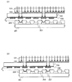
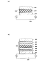
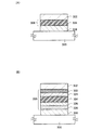
図1(A)は蒸着用基板110である。図1(A)において、第1の支持基板101の表面に反射層103が形成されている。反射層103は島状又はストライプ状の開口部を有している。また、反射層103と、第2の支持基板105の裏面が接して配置されている。第2の支持基板105の表面には、島状又はストライプ状にパターン形成された光吸収層107が形成されている。また、光吸収層107上には、材料層109が形成されている。図1(A)においては、材料層109は、第2の支持基板105全面を覆うように形成されている。
FIG. 1A shows a
第1の支持基板101は、反射層103の支持基板であり、発光装置の作製工程において、材料層を加熱する為に照射する光を透過する基板である。よって、第1の支持基板101は、光の透過率の高い基板であることが好ましい。具体的には、材料層109を蒸着するためにランプ光やレーザ光を用いた場合、第1の支持基板101として、それらの光を透過する基板を用いることが好ましい。第1の支持基板としては、例えば、ガラス基板、石英基板、無機ガラスを含むプラスチック基板などを用いることができる。
The
反射層103は、発光装置の作製工程において、材料層109を加熱するために照射する光を反射して、反射層103と重なる領域に配置された材料層109に、蒸着に必要な熱を与えないように遮断する層である。反射層103は、照射される光に対して、反射率が85%以上、さらに好ましくは、90%以上の高い反射率を有する材料で形成されていることが好ましい。例えば、800nm乃至2500nmの赤外領域の光を照射する場合、反射層103の材料として、銀、金、白金、銅、アルミニウム、アルミニウムを含む合金、または、銀を含む合金などを用いることができる。特に、アルミニウム−チタン合金、アルミニウム−ネオジム合金、銀−ネオジム合金は、赤外領域の光(波長800nm以上)に対して高い反射率を有しているため、反射層として好適に用いることができる。例えば、アルミニウム−チタン合金膜は、膜厚が400nmの場合、赤外領域(波長800nm以上2500nm以下)にわたって、85%以上の反射率を示し、特に、波長が900nm以上2500nm以下の範囲については90%以上の反射率を示す。なお、第1の支持基板101に照射する光の波長により、反射層103に好適な材料の種類は変化する。また、反射層は一層に限らず複数の層により構成されていてもよい。
The
さらに好ましくは、反射層103は、熱伝導率の低い材料で形成されていることが好ましい。熱伝導率の低い材料を用いることにより、被成膜基板へのEL層の微細なパターン形成が可能となる。
More preferably, the
また、反射層103は一層に限らず複数の層により構成されていてもよい。例えば、反射率の高い材料からなる膜と熱伝導率の低い材料からなる膜を積層して、反射層として用いても良い。
The
反射層103は、種々の方法を用いて形成することができる。例えば、スパッタリング法、電子ビーム蒸着法、真空蒸着法などにより形成することができる。また、反射層の膜厚は、材料により異なるが、概ね100nm以上2μm以下であることが好ましい。100nm以上であることにより、照射した光が反射層を透過することを抑制できる。
The
また、反射層103に開口部を形成する際には種々の方法を用いることができるが、ドライエッチングを用いることが好ましい。ドライエッチングを用いることにより、開口部の側壁が垂直に近い形状となり、微細なパターンを形成することができる。
Various methods can be used for forming the opening in the
第2の支持基板105は、光吸収層107及び材料層109の支持基板であり、発光装置の作製工程において、材料層109を加熱するために照射する光を透過する基板である。よって、第2の支持基板105は、光の透過率の高い基板であることが好ましい。具体的には、材料層109を蒸着するための光源にランプ光やレーザ光を用いた場合、第2の支持基板105として、それらの光を透過する基板を用いることが好ましい。また、第2の支持基板105としては、熱伝導率が低い材料を用いることが好ましい。熱伝導率が低いことにより、第1の支持基板101上に形成された反射層103が加熱された場合でも、反射層103に接する第2の支持基板105を介して光吸収層107に熱が伝わることを抑制することができ、反射層103と重なる領域に位置する材料層109が加熱されて蒸着するのを防止できる。第2の支持基板としては、例えば、ガラス基板、石英基板、無機ガラスを含むプラスチック基板などを用いることができる。
The
光吸収層107は発光装置の作製工程において、材料層109を加熱するために照射する光を吸収して熱へと変換する層である。光吸収層107は、照射される光に対して、70%以下の低い反射率を有し、また、高い吸収率を有する材料で形成されていることが好ましい。また、光吸収層107は、それ自体が熱によって変化しないように、耐熱性に優れた材料で形成されていることが好ましい。光吸収層107は一層に限らず複数の層により構成されていてもよい。光吸収層107は、反射層103の開口部と重なる領域に配置されている。また、反射層の開口部を透過した光が、光吸収層107で吸収され、当該領域の光吸収層と接する材料層109を加熱するため、光吸収層107は、被成膜基板に形成される画素と概略同じ大きさにパターン形成されているのが好ましい。なお、光吸収層107をストライプ状とする場合は、被成膜基板に形成される画素の幅と光吸収層107の幅を概略等しく形成するのが好ましい。
The
反射層103の開口部は、N箇所(Nは2以上の整数)の光吸収層107のパターンに対して1箇所の間隔で設けられているのが好ましく、3箇所の光吸収層107のパターンに対して1箇所の間隔で設けられていることがより好ましい。N箇所の光吸収層107のパターンに対して1箇所の反射層103の開口部を設けることで、N回の転写工程によって、光吸収層107の第1乃至第Nの領域上に位置する材料層109がそれぞれ加熱されて、光吸収層107の第1乃至第Nの全ての領域上に位置する材料層109を被成膜基板201に転写することができる。例えば、3箇所の光吸収層107のパターンに対して1箇所の間隔で反射層103の開口部が設けられている場合、3回の転写工程によって、第1乃至第3の領域の光吸収層107上に位置する材料層109を被成膜基板201に転写することができる。
The openings of the
また、3箇所の光吸収層107のパターンに対して1箇所の間隔で反射層103の開口部を設けることで、一度の転写工程で2画素おきに材料層を被成膜基板へと転写することができるため、被成膜基板を用いてフルカラー表示可能な表示装置を作製する場合に有効となる。本実施の形態においては、3箇所の光吸収層107のパターンに対して、1箇所の間隔で反射層103の開口部が設けられた蒸着用基板を用いて、フルカラー表示に対応する被成膜基板を作製する工程を例に説明する。
Further, by providing the openings of the
光吸収層107に好適な材料の種類は、材料層を加熱するために照射する光の波長により異なる。例えば、波長800nmの光に対しては、モリブデン、窒化タンタル、チタン、タングステンなどを用いることが好ましい。また、波長1300nmの光に対しては、窒化タンタル、チタンなどを用いることが好ましい。
The kind of material suitable for the
なお、モリブデン膜およびタングステン膜は、例えば、膜厚400nmとした場合、波長800nm以上900nm以下の光に対しては、反射率が60%以下であるため、光吸収層として好適に用いることができる。また、波長2000nm〜2500nmの光に対しては、反射率が85%以上であるため、反射層として用いることができる。 Note that when the film thickness is 400 nm, for example, the molybdenum film and the tungsten film have a reflectance of 60% or less for light with a wavelength of 800 nm to 900 nm, and thus can be suitably used as a light absorption layer. . In addition, for light with a wavelength of 2000 nm to 2500 nm, the reflectance is 85% or more, so that it can be used as a reflective layer.
光吸収層107は、種々の方法を用いて形成することができる。例えば、スパッタリング法で、モリブデン、タンタル、チタン、タングステンなどのターゲット、またはこれらの合金を用いたターゲットを用い、光吸収層107を形成することができる。また、光吸収層は一層に限らず複数の層により構成されていてもよい。
The
なお、光吸収層107をパターン形成する際には、種々の方法を用いることができるが、ドライエッチングを用いることが好ましい。ドライエッチングを用いることにより、パターン形成された光吸収層107の側壁が垂直に近い形状となり、微細なパターンを形成することができる。
Note that various methods can be used to pattern the
光吸収層の膜厚は、照射される光が透過しない膜厚であることが好ましい。材料によって異なるが、100nm以上2μm以下の膜厚であることが好ましい。特に、光吸収層107の膜厚を200nm以上600nm以下とすることで、照射される光を効率良く吸収して発熱させることができる。
The film thickness of the light absorbing layer is preferably a film thickness that does not transmit irradiated light. Although it varies depending on the material, the film thickness is preferably 100 nm or more and 2 μm or less. In particular, by setting the thickness of the
なお、光吸収層107は、材料層109に含まれる蒸着材料が昇華温度まで加熱されるのであれば、照射する光の一部が透過してもよい。ただし、一部が透過する場合には、光が照射しても分解しない材料を、材料層109に用いることが好ましい。
Note that the
なお、反射層と光吸収層の反射率は差が大きいほど好ましい。具体的には、照射する光の波長に対して、反射率の差が25%以上、より好ましくは30%以上であることが好ましい。 In addition, it is so preferable that the reflectance of a reflection layer and a light absorption layer is large. Specifically, the difference in reflectance with respect to the wavelength of light to be irradiated is preferably 25% or more, more preferably 30% or more.
材料層109は加熱により転写される層である。材料層に含まれる蒸着材料としては、種々の材料が挙げられる。また、材料層109は複数の材料を含んでいてもよい。また、材料層109は、単層でもよいし、複数の層が積層されていてもよい。材料層を複数積層することにより、共蒸着することが可能である。なお、材料層を複数積層する場合には、第2の支持基板105側に分解温度が低い蒸着材料を含むように積層されていることが好ましい。または、第2の支持基板105側に蒸着温度が低い蒸着材料を含むように積層されていることが好ましい。このような構成とすることにより、蒸着材料を含む複数の材料層を効率良く加熱することができ、蒸着することができる。なお、本明細書において「蒸着温度」とは、材料が昇華する温度を示す。また、「分解温度」とは、熱の作用によって、材料を示す化学式の少なくとも一部に変化が起こる温度を示す。
The
材料層109は、種々の方法により形成される。例えば、乾式法である真空蒸着法、スパッタリング法等を用いることができる。また、湿式法であるスピンコート法、スプレーコート法、インクジェット法、ディップコート法、キャスト法、ダイコート法、ロールコート法、ブレードコート法、バーコート法、グラビアコート法、又は印刷法等を用いることができる。これら湿式法を用いて材料層109を形成するには、所望の蒸着材料を溶媒に溶解あるいは分散させ、溶液あるいは分散液を調整すればよい。溶媒は、蒸着材料を溶解あるいは分散させることができ、且つ蒸着材料と反応しないものであれば特に限定されない。例えば、クロロホルム、テトラクロロメタン、ジクロロメタン、1,2−ジクロロエタン、或いはクロロベンゼンなどのハロゲン系溶媒、アセトン、メチルエチルケトン、ジエチルケトン、n−プロピルメチルケトン、或いはシクロヘキサノンなどのケトン系溶媒、ベンゼン、トルエン、或いはキシレンなどの芳香族系溶媒、酢酸エチル、酢酸n−プロピル、酢酸n−ブチル、プロピオン酸エチル、γ−ブチロラクトン、或いは炭酸ジエチルなどのエステル系溶媒、テトラヒドロフラン、或いはジオキサンなどのエーテル系溶媒、ジメチルホルムアミド、或いはジメチルアセトアミドなどのアミド系溶媒、ジメチルスルホキシド、ヘキサン、又は水等を用いることができる。また、これらの溶媒複数種を混合して用いてもよい。湿式法を用いることにより、材料の利用効率を高めることができ、発光装置を作製するコストを低減することができる。
The
なお、後の工程で被成膜基板201上に形成されるEL層の膜厚および均一性は、第2の支持基板105上に形成された材料層109に依存する。従って、均一に材料層109を形成することが重要となってくる。なお、EL層の膜厚および均一性が保たれるのであれば、材料層109は必ずしも均一の層である必要はない。例えば、微細な島状に形成されていてもよいし、凹凸を有する層状に形成されていてもよい。また、材料層109の膜厚を制御することにより、容易に被成膜基板201上に形成されるEL層207の膜厚を制御することができる。
Note that the thickness and uniformity of the EL layer formed over the
なお、蒸着材料としては、有機化合物、無機化合物、又は、無機化合物を含有する有機化合物にかかわらず、種々の材料を用いることができる。特に、有機化合物は無機化合物に比べ、蒸着温度が低い材料が多いため、光の照射により蒸着することが容易であり、発光装置の作製方法に好適である。例えば、有機化合物としては、発光装置に用いられる発光材料、キャリア輸送材料などが挙げられる。また、無機化合物としては、発光装置のキャリア輸送層やキャリア注入層、電極などに用いられる金属酸化物、金属窒化物、ハロゲン化金属、金属単体などがあげられる。 Note that various materials can be used as a deposition material regardless of an organic compound, an inorganic compound, or an organic compound containing an inorganic compound. In particular, since an organic compound has many materials having a lower deposition temperature than an inorganic compound, it can be easily deposited by light irradiation and is suitable for a method for manufacturing a light-emitting device. For example, examples of the organic compound include a light emitting material used for a light emitting device, a carrier transport material, and the like. Examples of the inorganic compound include metal oxides, metal nitrides, metal halides, and single metals used for carrier transport layers, carrier injection layers, and electrodes of light-emitting devices.
なお、図1(A)において、反射層103の開口部と、光吸収層107の第1の領域と、が重なるように、第1の支持基板101と第2の支持基板105が位置合わせされている。第1の支持基板101及び第2の支持基板105の少なくとも一方には、位置合わせ用のマーカを設けることが好ましい。なお、第1の支持基板101において、位置合わせのマーカ周辺の反射層103は予め除去しておくのが好ましく、第2の支持基板105において、位置合わせのマーカ周辺の光吸収層及び材料層は予め除去しておくことが好ましい。
Note that in FIG. 1A, the
次に、図1(B)に示すように、蒸着用基板110において、光吸収層107および材料層109が形成された面に対向する位置に、被成膜基板201を配置する。被成膜基板201は、蒸着処理により所望のEL層が成膜される基板である。そして、蒸着用基板110と被成膜基板201とを至近距離、具体的には蒸着用基板110に設けられた材料層109の表面と被成膜基板201との距離dを、0mm以上2mm以下、好ましくは0mm以上0.05mm以下、より好ましくは0mm以上0.03mm以下となるように近づけて近接させる。
Next, as illustrated in FIG. 1B, the
なお、距離dは、第2の支持基板105上に形成された材料層109の表面と、被成膜基板201の表面との距離で定義する。また、被成膜基板201上に何らかの層(例えば、電極として機能する導電層や隔壁として機能する絶縁層等)が形成されている場合、距離dは、材料層109の表面と、被成膜基板上に形成された層の表面との距離で定義する。ただし、材料層109或いは被成膜基板201上に形成された層の表面に凹凸を有する場合は、距離dは、材料層109の最表面と、被成膜基板或いは被成膜基板上に形成された層の最表面との間の最も短い距離で定義する。
Note that the distance d is defined as the distance between the surface of the
距離dを小さくすることで、材料の利用効率を向上させることができる。また、被成膜基板に形成される層のパターン形成の精度を向上させることができる。なお、材料の利用効率を向上させるため、また、パターン形成の精度を向上させるために、蒸着用基板110と被成膜基板201の基板間の距離は短いほうが好ましいが、本発明はこれに限定されるものではない。
By reducing the distance d, the material utilization efficiency can be improved. In addition, the accuracy of pattern formation of layers formed on the deposition target substrate can be improved. Note that the distance between the
図1(B)、(C)において、被成膜基板201は、第1の電極層203を有している。第1の電極層203の端部は絶縁物205で覆われていることが好ましい。絶縁物205を設けることで、距離dを0mmとした場合、すなわち蒸着用基板110の最表面と被成膜基板201の最表面が接している場合にも、第2または第3の領域の光吸収層107上に位置する材料層109と、画素形成領域と、が接するのを防ぐことができる。本実施の形態において、第1の電極層203は、発光素子の陽極あるいは陰極となる電極を示している。
In FIGS. 1B and 1C, the
なお、図1(B)において、反射層103の開口部と、第1の電極層203とが重なるように、蒸着用基板110と被成膜基板201が位置合わせされている。よって、被成膜基板には、位置合わせ用のマーカを設けることが好ましい。また、第2の支持基板105にも、位置合わせ用のマーカを設けることが好ましい。なお、第2の支持基板105において、位置合わせのマーカ周辺の光吸収層107及び材料層109は予め除去しておくのが好ましい。また、蒸着用基板110と被成膜基板201との位置合わせに用いるマーカは、第1の支持基板101と第2の支持基板105との位置合わせに用いたマーカと兼用することができる。
Note that in FIG. 1B, the
そして、図1(C)に示すように、蒸着用基板110の第1の支持基板101側から光を照射する。照射された光は、反射層103が形成された領域においては反射し、反射層103に設けられた開口部においては透過して、開口部と重なる光吸収層107の第1の領域において吸収される。吸収された光が熱エネルギーへと変換されることで、当該領域の光吸収層107と接する材料層109が加熱され、蒸着材料が第1の電極層上に蒸着される。これによってEL層207が成膜される(第1の転写工程)。
Then, as shown in FIG. 1C, light is irradiated from the
なお、反射率が85%以上の材料を用いて反射層103を形成したとしても、蒸着用基板110に光を照射した際に、照射する光の熱量によっては、ある程度の熱の吸収が考えられる。しかしながら、蒸着用基板としては、反射層103に接して、熱伝導率の低い材料を用いた第2の支持基板105が設けられていることが好ましく、反射層103が加熱された場合であっても、第2の支持基板105において光吸収層107への熱の伝導を遮断することができる。また、光吸収層107は、島状またはストライプ状にパターン形成されているため、光吸収層が第2の支持基板105の全面に形成されている場合と比較して、光吸収層107で発生した熱が面方向に伝導するのを防ぐことができる。これによって、反射層103の開口部と重なる領域の材料層109を選択的に加熱して、被成膜基板上に高精度で所望のパターンを有するEL層207を形成することができる。
Note that even when the
本実施の形態において、第1の支持基板101、第2の支持基板105及び被成膜基板201は、同じ材質の基板を用いることが好ましい。第1の支持基板101、第2の支持基板105及び被成膜基板を同じ材質とすることで、当該3枚の基板の有する熱膨張率を等しくすることができる。したがって、蒸着用基板に光を照射した際に、蒸着用基板が熱によって膨張した場合であっても、被成膜基板も同じ熱膨張率で膨張するため、膨張率の違いによる転写精度の低減を抑制することができる。なお、第1の支持基板101、第2の支持基板105及び被成膜基板201は、必ずしも同じ材質の基板とする必要はなく、熱膨張率の差異が転写精度に影響を与えない程度近似している場合は、異なる材質の基板を用いても構わない。
In this embodiment mode, the
また、蒸着用基板は、従来の遮光マスクに変えて、開口部を有する反射層103が設けられた第1の支持基板101を用いている。第1の支持基板101において、反射層103の開口部は、フォトリソグラフィ法によって形成されているため、開口部の側壁を垂直に近い形状に、かつ反射層の上面を平坦に形成することができ、第1の支持基板101と第2の支持基板105の密着性も向上する。第1の支持基板101と第2の支持基板105を密着させることで、反射層103と第2の支持基板105との隙間から光が入り込むのを防ぐことができるため、所望の光吸収層を精度良く照射することが可能となる。さらに、第1の支持基板101として、例えば、ガラス基板、石英基板、無機ガラスを含むプラスチック基板などを用いると、従来の遮光マスクと比較してハンドリングが容易であるため、好ましい。
In addition, the deposition substrate uses a
照射する光の光源としては、種々の光源を用いることができる。 Various light sources can be used as the light source of the light to be irradiated.
例えば、レーザ光の光源としては、Arレーザ、Krレーザ、エキシマレーザなどの気体レーザ、単結晶のYAG、YVO4、フォルステライト(Mg2SiO4)、YAlO3、GdVO4、若しくは多結晶(セラミック)のYAG、Y2O3、YVO4、YAlO3、GdVO4に、ドーパントとしてNd、Yb、Cr、Ti、Ho、Er、Tm、Taのうち1種または複数種添加されているものを媒質とするレーザ、ガラスレーザ、ルビーレーザ、アレキサンドライトレーザ、Ti:サファイアレーザ、銅蒸気レーザまたは金蒸気レーザのうち一種または複数種から発振されるものを用いることができる。また、レーザ媒体が固体である固体レーザを用いると、メンテナンスフリーの状態を長く保てるという利点や、出力が比較的に安定している利点を有している。 For example, the laser light source may be a gas laser such as an Ar laser, a Kr laser, or an excimer laser, single crystal YAG, YVO 4 , forsterite (Mg 2 SiO 4 ), YAlO 3 , GdVO 4 , or polycrystalline (ceramic) ) YAG, Y 2 O 3 , YVO 4 , YAlO 3 , GdVO 4 and one or more of Nd, Yb, Cr, Ti, Ho, Er, Tm, and Ta as dopants. Lasers oscillated from one or more of lasers, glass lasers, ruby lasers, alexandrite lasers, Ti: sapphire lasers, copper vapor lasers or gold vapor lasers can be used. In addition, when a solid-state laser whose laser medium is solid is used, there are advantages that a maintenance-free state can be maintained for a long time and output is relatively stable.
また、レーザ光以外の光源としては、キセノンランプ、メタルハライドランプのような放電灯、ハロゲンランプ、タングステンランプのような発熱灯を用いることができる。また、これらの光源をフラッシュランプ(例えば、キセノンフラッシュランプ、クリプトンフラッシュランプなど)として用いてもよい。フラッシュランプは短時間(0.1ミリ秒乃至10ミリ秒)で非常に強度の高い光を繰り返し、大面積に照射することができるため、蒸着用基板の面積にかかわらず、効率よく均一に加熱することができる。また、発光させる時間の長さを変えることによって蒸着用基板の加熱の制御もできる。また、フラッシュランプは寿命が長く、発光待機時の消費電力が低いため、ランニングコストを低く抑えることができる。 Further, as a light source other than the laser light, a discharge lamp such as a xenon lamp or a metal halide lamp, or a heating lamp such as a halogen lamp or a tungsten lamp can be used. These light sources may be used as flash lamps (for example, xenon flash lamps, krypton flash lamps, etc.). The flash lamp can irradiate a large area repeatedly in a short time (0.1 ms to 10 ms), so that it can be heated efficiently and uniformly regardless of the area of the evaporation substrate. can do. In addition, heating of the evaporation donor substrate can be controlled by changing the length of time for light emission. Moreover, since the flash lamp has a long life and low power consumption during light emission standby, the running cost can be kept low.
なお、照射する光としては、赤外光(波長800nm以上)であることが好ましい。赤外光であることにより、光吸収層107が効率よく加熱され、蒸着材料を効率よく加熱することができる。
In addition, it is preferable that it is infrared light (wavelength 800nm or more) as light to irradiate. By being infrared light, the
ここで、反射層103の開口部は、3箇所の光吸収層107のパターンに対して1箇所の間隔で設けられているため、材料層109も反射層103の開口部の繰り返しパターンに合わせて転写され、その間は光吸収層107上に材料層109が残った状態となる。本実施の形態の蒸着用基板は、反射層103が形成された第1の支持基板101と、光吸収層107及び材料層109が形成された第2の支持基板105の2枚の支持基板によって構成されているため、この2枚の支持基板の位置関係をずらすことによって、第1の転写工程で残った材料層109を、次の転写においても利用することができる。
Here, since the openings of the
図2(A)は、上述した第1の転写工程で使用した蒸着用基板110を用いた、第2の転写工程を示す。図2(A)に示す第2の転写工程においては、反射層103の開口部と、光吸収層107の第2の領域と、が重なるように、第1の支持基板101と第2の支持基板105が位置合わせされている。よって、第1の支持基板101及び第2の支持基板105の少なくとも一方には、第2の転写工程に対応する位置合わせ用のマーカを設けることが好ましい。なお、光吸収層107の第2の領域は、先の転写工程で光が照射された光吸収層107の第1の領域に隣接する領域であり、第1の支持基板101及び第2の支持基板105のどちらか、又は双方を、光吸収層のパターンの間隔分シフトさせて配置させればよい。
FIG. 2A shows a second transfer process using the
第1の支持基板101と第2の支持基板105を位置合わせした蒸着用基板110を、被成膜基板201と対向配置して、位置合わせをする。よって、蒸着用基板110及び被成膜基板201の少なくとも一方には、第2の転写工程に対応する位置合わせ用のマーカを設けることが好ましい。蒸着用基板110と被成膜基板201とは第1の転写工程とは、蒸着用基板110の幅分ずらして配置されている。なお、本実施の形態の蒸着用基板110を用いて、単色表示に対応する被成膜基板を作製する場合には、蒸着用基板110の開口部及び被成膜基板201を、第1の転写工程とは、1画素分ずらして配置するのが好ましい。また、位置合わせの際には、蒸着用基板110及び被成膜基板201のどちらを移動させても良く、双方を移動させても良い。または、被成膜基板201を移動させる代わりに、別の被成膜基板と対向配置させてもよい。
The
位置合わせを行った後は、蒸着用基板110の第1の支持基板101側から光を照射する。照射された光は、反射層103が形成された領域においては反射し、反射層103に設けられた開口部においては透過して、開口部と重なる光吸収層107の第2の領域において吸収される。吸収された光が熱エネルギーへと変換されることで、当該領域の光吸収層107と接する材料層109が加熱され、蒸着材料が第1の電極層上に蒸着される。これによってEL層207が成膜される(第2の転写工程)。
After alignment, light is irradiated from the
図2(B)は、上述した第1及び第2の転写工程で使用した蒸着用基板110を用いた、第3の転写工程を示す。図2(B)に示す第3の転写工程においては、反射層103の開口部と、光吸収層107の第3の領域と、が重なるように、第1の支持基板101と第2の支持基板105が位置合わせされている。よって、第1の支持基板101及び第2の支持基板105の少なくとも一方には、第3転写工程に対応する位置合わせ用のマーカを設けることが好ましい。なお、光吸収層107の第3の領域は、第2の転写工程で光が照射された光吸収層107の第2の領域に隣接する領域であり、第1の支持基板101及び第2の支持基板105のどちらか、又は双方を、光吸収層のパターンの間隔分シフトさせて配置させればよい。
FIG. 2B shows a third transfer process using the
第1の支持基板101と第2の支持基板105を位置合わせした蒸着用基板110を、被成膜基板201と対向配置して、位置合わせをする。よって、蒸着用基板110及び被成膜基板201の少なくとも一方には、第3の転写工程に対応する位置合わせ用のマーカを設けることが好ましい。蒸着用基板110と被成膜基板201とは第2の転写工程とは、蒸着用基板110の幅分ずらして配置されている。なお、本実施の形態の蒸着用基板110を用いて、単色表示に対応する被成膜基板を作製する場合には、蒸着用基板110の開口部及び被成膜基板201を、第2の転写工程とは、1画素分ずらして配置するのが好ましい。また、位置合わせの際には、蒸着用基板110及び被成膜基板201のどちらを移動させても良く、双方を移動させても良い。または、被成膜基板201を移動させる代わりに、別の被成膜基板と対向配置させてもよい。
The
位置合わせを行った後は、蒸着用基板110の第1の支持基板101側から光を照射する。照射された光は、反射層103が形成された領域においては反射し、反射層103に設けられた開口部においては透過して、開口部と重なる光吸収層107の第3の領域において吸収される。吸収された光が熱エネルギーへと変換されることで、当該領域の光吸収層107と接する材料層109が加熱され、蒸着材料が第1の電極層上に蒸着される。これによってEL層207が成膜される(第3の転写工程)。
After alignment, light is irradiated from the
以上示した第1乃至第3の転写工程によって、蒸着用基板110上に形成された第1乃至第3の領域の光吸収層上の全ての領域の材料層109を被成膜基板201に転写することができる。
Through the first to third transfer steps shown above, the
本実施の形態の発光装置の作製方法において、輻射熱ではなく、光源からの光で光吸収層を加熱させることが特徴である。また、蒸着用基板110に形成された材料層109の全てが蒸着されないようにするため、光を照射する時間は、比較的短くてよい。例えば、ハロゲンランプを光源として用いた場合、500℃〜800℃を7〜15秒間程度保持することで、材料層を蒸着することができる。
In the method for manufacturing the light-emitting device of this embodiment mode, the light absorption layer is heated with light from a light source instead of radiant heat. In addition, in order to prevent the
また、成膜は減圧雰囲気で行われることが好ましい。減圧雰囲気は、成膜室内を真空排気手段により真空度が5×10⁻³Pa以下、好ましくは10−4Pa乃至10−6Pa程度の範囲になるように真空排気することで得られる。 The film formation is preferably performed in a reduced pressure atmosphere. The reduced-pressure atmosphere can be obtained by evacuating the film forming chamber so that the degree of vacuum is 5 × 10 −3 Pa or less, preferably in the range of about 10 −4 Pa to 10 −6 Pa.
また、光源として、レーザ光などの指向性が高い光源を用いる場合には、反射層103の開口部を透過した光が指向性を持って光吸収層107に照射され、光吸収層107の光が照射された部分に接する材料層109が加熱される。つまり、反射層103の開口部を通過した光の広がりが少ない。よって、反射層103の開口部に対応する領域とほぼ同じ範囲の材料層109が蒸着されるため、反射層103の開口部の幅及び光吸収層107のパターンの幅は画素の幅と概略等しくすることができる。また、照射する光のまわりこみが少ないため、光を照射する面から見て、反射層103の端部の位置と光吸収層107の端部の位置が揃っている構成としてもよい。
When a light source with high directivity such as laser light is used as the light source, light transmitted through the opening of the
一方、光源として、フラッシュランプなどの指向性が低い光源を用いる場合には、反射層103の開口部を通過した光が第2の支持基板105を通過する間に広がって、光吸収層107に照射されるという現象が起こる。そして、反射層103の開口部に対応する領域よりも広範囲の材料層109が蒸着される。したがって、照射する光が広がることを考慮して、反射層103の開口部を画素の大きさよりも小さくすることが好ましい。また、反射層103の開口部の大きさを光吸収層107のパターンの幅よりも小さくすることが望ましい。
On the other hand, when a light source with low directivity, such as a flash lamp, is used as the light source, the light that has passed through the opening of the
また、本実施の形態では、被成膜基板201が、蒸着用基板110の下方に位置する場合を図示したが、本発明はこれに限定されない。基板の設置する向きは適宜設定することができる。
Further, although the case where the
本実施の形態の発光装置に適用する成膜方法は、第2の支持基板に形成した材料層109の膜厚によって、蒸着処理により被成膜基板201に成膜されるEL層207の膜厚を制御することができる。つまり、第2の支持基板105に成膜した材料層109をそのまま蒸着すればよいため、膜厚モニターが不要である。よって、膜厚モニターを利用した蒸着速度の調節を使用者が行う必要がなく、成膜工程を全自動化することが可能である。そのため、生産性の向上を図ることができる。
The film formation method applied to the light-emitting device of this embodiment is based on the film thickness of the
また、本実施の形態の発光装置に適用する成膜方法は、材料層109に含有される蒸着材料を均一に加熱することができる。また、材料層109が複数の蒸着材料を含む場合、材料層109と同じ蒸着材料を略同じ重量比で含有するEL層207を被成膜基板201に成膜することができる。このように、本発明に係る成膜方法は、蒸着温度の異なる複数の蒸着材料を用いて成膜する場合、共蒸着のようにそれぞれ蒸着レートを制御する必要がない。そのため、蒸着レート等の複雑な制御を行うことなく、所望の異なる蒸着材料を含む層を容易に精度良く成膜することができる。
In addition, the deposition method applied to the light-emitting device of this embodiment can uniformly heat the evaporation material contained in the
また、本発明の一態様である蒸着用基板を適用することで、平坦でムラのない膜を成膜することが可能となる。また、発光層のパターン形成が容易となるため、発光装置の製造も簡便となる。また、微細なパターン形成が可能となるため、高精細な発光装置を得ることができる。また、光源として、レーザ光だけでなく、安価ではあるが熱量の大きなランプヒーター等を用いることができる。また、光源として、ランプヒーター等を用いることにより、大面積を一括して成膜することが可能となるため、タクト時間を短縮することができる。よって、発光装置の作製コストを削減することができる。 In addition, by using the evaporation substrate which is one embodiment of the present invention, a flat and uniform film can be formed. Moreover, since the pattern formation of the light emitting layer is facilitated, the manufacture of the light emitting device is also simplified. In addition, since a fine pattern can be formed, a high-definition light-emitting device can be obtained. As the light source, not only a laser beam but also a lamp heater with a large amount of heat although it is inexpensive can be used. In addition, by using a lamp heater or the like as the light source, it is possible to form a film over a large area, so that the tact time can be shortened. Thus, the manufacturing cost of the light-emitting device can be reduced.
また、本発明の一態様である成膜方法は、所望の蒸着材料を無駄にすることなく、被成膜基板に成膜することが可能である。よって、蒸着材料の利用効率が向上し、コスト削減を図ることができる。また、成膜室内壁に蒸着材料が付着することも防止でき、成膜装置のメンテナンスを簡便にすることができる。 In addition, the film formation method which is one embodiment of the present invention can form a film on a deposition target substrate without wasting a desired vapor deposition material. Therefore, the utilization efficiency of the vapor deposition material is improved, and the cost can be reduced. Further, it is possible to prevent the deposition material from adhering to the wall of the film formation chamber, and the maintenance of the film formation apparatus can be simplified.
よって、この成膜方法を適用することで、所望の異なる蒸着材料を含む層の成膜が容易になり、当該異なる蒸着材料を含む層を用いた発光装置等の製造における生産性を向上させることが可能となる。 Therefore, by applying this film formation method, it becomes easy to form a layer containing a desired different vapor deposition material, and to improve productivity in manufacturing a light-emitting device using the layer containing the different vapor deposition material. Is possible.
また、本実施の形態の蒸着用基板を用いることにより、蒸着材料の利用効率良く成膜することが可能となり、コスト削減を図ることができる。また、本実施の形態の蒸着用基板を用いることにより、精度良く、所望の形状の膜を形成することが可能となる。 In addition, with the use of the evaporation donor substrate of this embodiment, it is possible to form a film with high use efficiency of the evaporation material, and cost can be reduced. Further, by using the evaporation donor substrate of this embodiment, a film having a desired shape can be formed with high accuracy.
なお、本実施の形態は、本明細書で示す他の実施の形態と適宜組み合わせることができる。 Note that this embodiment can be combined with any of the other embodiments described in this specification as appropriate.
(実施の形態2)
本実施の形態では、上記実施の形態で説明した蒸着用基板を用いてフルカラー表示装置を作製する方法について説明する。
(Embodiment 2)
In this embodiment, a method for manufacturing a full-color display device using the evaporation donor substrate described in the above embodiment will be described.
実施の形態1では、1枚の蒸着用基板を用いて、2画素おきに1色のEL層を形成する例を示しているが、フルカラー表示装置を作製する場合には、複数回の成膜工程に分けて、発光色の異なる発光層をそれぞれ異なる領域に形成する。 In Embodiment Mode 1, an example in which an EL layer of one color is formed every two pixels by using one evaporation deposition substrate is shown. However, in the case of manufacturing a full-color display device, film formation is performed a plurality of times. Dividing into processes, light emitting layers having different emission colors are formed in different regions.
フルカラー表示可能な発光装置の作製例を以下に説明する。ここでは、3色の発光層を用いる発光装置の例を示す。 An example of manufacturing a light emitting device capable of full color display will be described below. Here, an example of a light emitting device using a light emitting layer of three colors is shown.
図1(A)に示す蒸着用基板を3枚用意する。それぞれの蒸着用基板には、それぞれ異なる蒸着材料を含む材料層を形成する。具体的には、赤色発光層用の材料層を設けた第1の蒸着用基板と、緑色発光層用の材料層を設けた第2の蒸着用基板と、青色発光層用の材料層を設けた第3の蒸着用基板とを用意する。 Three deposition substrates shown in FIG. 1A are prepared. A material layer containing a different vapor deposition material is formed on each vapor deposition substrate. Specifically, a first deposition substrate provided with a material layer for a red light emitting layer, a second deposition substrate provided with a material layer for a green light emitting layer, and a material layer for a blue light emitting layer are provided. And a third deposition substrate.
また、第1の電極層が設けられた被成膜基板を1枚用意する。なお、隣り合う第1の電極層同士が短絡しないように、第1の電極層の端部を覆う隔壁となる絶縁物を設けることが好ましい。発光領域となる領域は、第1の電極層の一部、即ち絶縁物と重ならずに露呈している領域に相当する。 In addition, one deposition target substrate provided with the first electrode layer is prepared. Note that an insulator serving as a partition wall covering the end portion of the first electrode layer is preferably provided so that adjacent first electrode layers are not short-circuited. The region serving as the light emitting region corresponds to a part of the first electrode layer, that is, a region exposed without overlapping with the insulator.
そして、被成膜基板と第1の蒸着用基板とを重ね、位置合わせをした後、第1の蒸着用基板の第1の支持基板側から光を照射する。照射された光を、反射層の開口部上に位置する光吸収層が吸収することで、当該領域の光吸収層が発熱し、その光吸収層と接している赤色発光層用の材料層が加熱され、被成膜基板に設けられている第1の電極層上に、第1の蒸着用基板による第1の転写が行われる。また、第1の転写工程の後は、上記実施の形態で示したように、蒸着用基板を構成する第1又は第2の支持基板、あるいは被成膜基板を適宜移動させ、第2乃至第3の転写工程を行う。以上によって、赤色発光層用の材料層の成膜が行われる。第1の支持基板と第2の支持基板の配置をずらして複数回の転写に用いることで、赤色発光層用の材料層を効率よく利用することができる。成膜を終えたら、第1の蒸着用基板は、被成膜基板と離れた場所へ移動させる。 Then, after the deposition target substrate and the first deposition substrate are overlapped and aligned, light is irradiated from the first support substrate side of the first deposition substrate. The light absorbing layer located on the opening of the reflective layer absorbs the irradiated light, so that the light absorbing layer in the region generates heat, and the material layer for the red light emitting layer in contact with the light absorbing layer is formed. The first transfer by the first evaporation donor substrate is performed on the heated first electrode layer provided on the deposition target substrate. After the first transfer step, as shown in the above embodiment mode, the first or second support substrate or the deposition target substrate that constitutes the evaporation donor substrate is moved as appropriate, so that the second to second steps are performed. Step 3 is performed. As described above, the material layer for the red light emitting layer is formed. The material layer for the red light emitting layer can be efficiently used by shifting the arrangement of the first support substrate and the second support substrate and using them for a plurality of transfers. After the film formation is completed, the first evaporation donor substrate is moved to a place away from the deposition target substrate.
本実施の形態の蒸着用基板は、光吸収層がパターン形成されているため、光吸収層において変換された熱が光吸収層の面方向に伝導して、反射層の上部に位置する材料層が加熱されるのを防ぐことができる。また、反射層が加熱された場合であっても、第2の支持基板によって、光吸収層へ反射層の加熱により生じた熱が伝導するのを防ぐことができる。これによって、被成膜基板上に、精度良くEL層を形成することができる。 Since the light-absorbing layer is patterned in the deposition substrate of this embodiment, the heat converted in the light-absorbing layer is conducted in the surface direction of the light-absorbing layer, and the material layer is located above the reflective layer. Can be prevented from being heated. Even when the reflective layer is heated, the second support substrate can prevent conduction of heat generated by heating the reflective layer to the light absorption layer. Thus, the EL layer can be formed with high accuracy on the deposition target substrate.
次いで、被成膜基板と第2の蒸着用基板とを重ね、位置合わせをする。第2の蒸着用基板には、第1の蒸着用基板を用いて蒸着されたEL層とは1画素分ずらした領域と重なる位置に反射層の開口部が配置されている。 Next, the deposition target substrate and the second deposition substrate are overlapped and aligned. In the second vapor deposition substrate, an opening of the reflective layer is arranged at a position overlapping with a region shifted by one pixel from the EL layer deposited using the first vapor deposition substrate.
そして、第2の蒸着用基板の裏面側から光を照射する。照射された光を、反射層の開口部上に位置する光吸収層が吸収することで、当該領域の光吸収層が発熱し、その光吸収層と接している緑色発光層用の材料層が加熱され、被成膜基板に設けられている第1の電極層上に、第2の蒸着用基板による第1の転写が行われる。また、第1の転写工程の後は、上記実施の形態で示したように、蒸着用基板を構成する第1又は第2の支持基板、あるいは被成膜基板を適宜移動させ、第2乃至第3の転写工程を行う。以上によって、緑色発光層用の材料層の成膜が行われる。第1の支持基板と第2の支持基板の配置をずらして複数回の転写に用いることで、緑色発光層用の材料層を効率よく利用することができる。成膜を終えたら、第2の蒸着用基板は、被成膜基板と離れた場所へ移動させる。 Then, light is irradiated from the back side of the second evaporation donor substrate. The light absorbing layer located on the opening of the reflective layer absorbs the irradiated light, so that the light absorbing layer in the region generates heat, and the material layer for the green light emitting layer in contact with the light absorbing layer is formed. The first transfer by the second evaporation donor substrate is performed on the heated first electrode layer provided on the deposition target substrate. After the first transfer step, as shown in the above embodiment mode, the first or second support substrate or the deposition target substrate that constitutes the evaporation donor substrate is moved as appropriate, so that the second to second steps are performed. Step 3 is performed. As described above, the material layer for the green light emitting layer is formed. The material layer for the green light emitting layer can be efficiently used by shifting the arrangement of the first support substrate and the second support substrate and using them for multiple times of transfer. After the film formation is completed, the second evaporation donor substrate is moved to a place away from the deposition target substrate.
次いで、被成膜基板と第3の蒸着用基板とを重ね、位置合わせをする。第3の蒸着用基板には、第1の蒸着用基板を用いて蒸着されたEL層とは2画素分ずらした領域と重なる位置に反射層の開口部が配置されている。 Next, the deposition target substrate and the third evaporation donor substrate are overlapped and aligned. In the third evaporation donor substrate, an opening of the reflective layer is arranged at a position overlapping with a region shifted by two pixels from the EL layer evaporated using the first evaporation donor substrate.
そして、第3の蒸着用基板の裏面側から光を照射して3回目の成膜を行う。この3回目の成膜を行う直前の様子が図3(A)の上面図に相当する。反射層411は開口部412を有している。また、開口部412に対応する領域に光吸収層が形成されている。また、被成膜基板における開口部412に対応する領域は、第1の電極層が絶縁物413で覆われておらず露出している領域である。なお、図3(A)中に点線で示した領域の下方にある被成膜基板には、既に1回目で成膜された第1の膜(R)421と2回目で成膜された第2の膜(G)422が位置している。
Then, a third film is formed by irradiating light from the back side of the third evaporation donor substrate. The state immediately before the third film formation corresponds to the top view of FIG. The
そして、3回目の成膜により、第3の膜(B)423が形成される(図3(B))。照射された光が反射層の開口部を通過し、開口部に対応する領域に形成された光吸収層において吸収されると、当該領域の光吸収層が発熱する。これによって、開口部に対応する領域に形成された光吸収層と接している青色発光層用の材料層が加熱され、被成膜基板に設けられている第1の電極層上に、第3の蒸着用基板による第1の転写が行われる。また、第1の転写工程の後は、上記実施の形態で示したように、蒸着用基板を構成する第1又は第2の支持基板、あるいは被成膜基板を適宜移動させ、第2乃至第3の転写工程を行う。以上によって、青色発光層用の材料層の成膜が行われる。第1の支持基板と第2の支持基板の配置をずらして複数回の転写に用いることで、青色発光層用の材料層を効率よく利用することができる。成膜を終えたら、第3の蒸着用基板は、被成膜基板と離れた場所へ移動させる。 Then, a third film (B) 423 is formed by the third deposition (FIG. 3B). When the irradiated light passes through the opening of the reflection layer and is absorbed by the light absorption layer formed in the region corresponding to the opening, the light absorption layer in the region generates heat. Accordingly, the material layer for the blue light-emitting layer that is in contact with the light absorption layer formed in the region corresponding to the opening is heated, and the third electrode layer is formed on the first electrode layer provided on the deposition target substrate. The first transfer is performed by the deposition substrate. After the first transfer step, as shown in the above embodiment mode, the first or second support substrate or the deposition target substrate that constitutes the evaporation donor substrate is moved as appropriate, so that the second to second steps are performed. Step 3 is performed. As described above, the material layer for the blue light emitting layer is formed. By shifting the arrangement of the first support substrate and the second support substrate and using them for a plurality of transfers, the material layer for the blue light emitting layer can be used efficiently. After the film formation is completed, the third evaporation donor substrate is moved to a place away from the deposition target substrate.
こうして、第1の膜(R)421、第2の膜(G)422、第3の膜(B)423を一定の間隔をあけて選択的に形成する。そして、これらの膜上に第2の電極層を形成し、発光素子を形成する。 In this manner, the first film (R) 421, the second film (G) 422, and the third film (B) 423 are selectively formed with a certain interval. Then, a second electrode layer is formed over these films to form a light emitting element.
以上の工程でフルカラー表示装置を作製することができる。 Through the above process, a full-color display device can be manufactured.
図3では、蒸着用基板に形成された反射層の開口部412の形状を矩形とした例を示したが、特にこの形状に限定されず、ストライプ状の開口部としても良い。ストライプ状の開口部とした場合、同じ発光色となる発光領域の間にも成膜が行われるが、絶縁物413の上に形成されるため、絶縁物413と重なる部分は発光領域とはならない。
Although FIG. 3 shows an example in which the shape of the
また、画素の配列も特に限定されず、図4(B)に示すように、1つの画素形状を多角形、例えば六角形としてもよく、第1の膜(R)441、第2の膜(G)442、第3の膜(B)443を配置してフルカラー表示装置を実現してもよい。図4(B)に示す多角形の画素を形成するために、図4(A)に示す多角形の開口部432が設けられた反射層431を有する第1の支持基板と第2の支持基板を蒸着用基板として成膜すればよい。
The pixel arrangement is not particularly limited, and as shown in FIG. 4B, one pixel shape may be a polygon, for example, a hexagon, and the first film (R) 441, the second film ( G) 442 and the third film (B) 443 may be arranged to realize a full-color display device. In order to form the polygonal pixel shown in FIG. 4B, a first support substrate and a second support substrate each having a
本実施の形態を適用することで、発光素子を構成するEL層を容易に形成することができ、当該発光素子を有する発光装置の製造も簡便になる。また、発光層のパターン形成が容易となるため、発光装置の製造も簡便となる。また、微細なパターン形成が可能となるため、高精細な発光装置を得ることができる。また、光源として、レーザ光だけでなく、安価ではあるが熱量の大きなランプヒーター等を用いることができる。よって、発光装置の作製コストを削減することができる。 By applying this embodiment mode, an EL layer included in the light-emitting element can be easily formed, and a light-emitting device including the light-emitting element can be easily manufactured. Moreover, since the pattern formation of the light emitting layer is facilitated, the manufacture of the light emitting device is also simplified. In addition, since a fine pattern can be formed, a high-definition light-emitting device can be obtained. As the light source, not only a laser beam but also a lamp heater with a large amount of heat although it is inexpensive can be used. Thus, the manufacturing cost of the light-emitting device can be reduced.
また、本実施の形態を適用することにより、ホスト材料にドーパント材料が分散された発光層を形成する場合、共蒸着を適用する場合と比べ複雑な制御を必要としない。さらに、ドーパント材料の添加量等も制御し易いため、容易に精度良く成膜でき、所望の発光色も得られやすくなる。また、蒸着材料の利用効率も向上させることができるため、コスト削減を図ることもできる。 In addition, when this embodiment is applied, when forming a light emitting layer in which a dopant material is dispersed in a host material, complicated control is not required as compared with the case where co-evaporation is applied. Furthermore, since the addition amount of the dopant material and the like can be easily controlled, a film can be easily formed with high accuracy, and a desired emission color can be easily obtained. In addition, since the utilization efficiency of the vapor deposition material can be improved, the cost can be reduced.
なお、本実施の形態は、本明細書で示す他の実施の形態と適宜組み合わせることができる。 Note that this embodiment can be combined with any of the other embodiments described in this specification as appropriate.
(実施の形態3)
本実施の形態では、発光装置の作製を可能とする成膜装置の例について説明する。本実施の形態に係る成膜装置の断面の模式図を図5、図6に示す。
(Embodiment 3)
In this embodiment, an example of a film formation apparatus that can manufacture a light-emitting device will be described. 5 and 6 are schematic views of a cross section of the film forming apparatus according to this embodiment.
図5(A)において、成膜室801は、真空チャンバーであり、第1のゲート弁802、及び第2のゲート弁803によって他の処理室と連結している。また、成膜室801内には、蒸着用基板支持手段804である蒸着用基板支持機構と、被成膜基板支持手段805である被成膜基板支持機構と、光源810を少なくとも有している。
In FIG. 5A, a
まず、他の成膜室において、上記実施の形態で示した構成で、光吸収層を形成した第2の支持基板上に、材料層808を形成する。本実施の形態において、蒸着用基板は、第1の支持基板806及び第2の支持基板807を有する。また、第2の支持基板807は図1に示した第2の支持基板105に相当し、材料層109に相当する材料層808が設けられている。また、第1の支持基板806は、図1に示した第1の支持基板101に相当する。なお、図示していないが、第1の支持基板806と第2の支持基板807との間には、開口部を有する反射層が形成されており、また、第2の支持基板807と、材料層808との間には、上記実施の形態で示した構成で、光吸収層が形成されている。本実施の形態では、第1または第2の支持基板として、銅を主材料とした四角平板状の基板を用いる。また、材料層808としては、蒸着可能である材料を用いる。
First, in another deposition chamber, the
なお、第1の支持基板806及び第2の支持基板807としては、特に形状は限定されない。また、材料層808の形成方法は乾式法や湿式法を用いることができ、特に湿式法であることが好ましい。例えば、スピンコート法、印刷法、またはインクジェット法などを用いることができる。
Note that the shape of the
次いで、第1の支持基板806及び第2の支持基板807を成膜室801に搬送し、蒸着用基板支持機構にセットする。ここで、マーカによって、第1の支持基板806と第2の支持基板807とを位置合わせする。また、第2の支持基板807における材料層808の形成されている面と、被成膜基板809の被成膜面とが、対向するように、被成膜基板809を被成膜基板支持機構に固定する。
Next, the
被成膜基板支持手段805を移動させて、第2の支持基板807と被成膜基板809の基板間隔が距離dとなるように近づける。なお、距離dは、第2の支持基板807上に形成された材料層808の表面と、被成膜基板809の表面との距離で定義する。また、被成膜基板809上に何らかの層(例えば、電極として機能する導電層や隔壁として機能する絶縁層等)が形成されている場合、距離dは、第2の支持基板807上の材料層808の表面と、被成膜基板809上に形成された層の表面との距離で定義する。ただし、被成膜基板809或いは被成膜基板809上に形成された層の表面に凹凸を有する場合は、距離dは、第2の支持基板807上の材料層808の表面と、被成膜基板809或いは被成膜基板809上に形成された層の最表面との間の最も短い距離で定義する。また、被成膜基板809が石英基板のように硬く、ほとんど変形(反り、撓みなど)しない材料であれば、距離dは0mmを下限として近づけることができる。なお、距離dが0mmとは、被成膜基板の最表面と蒸着用基板の最表面とが接している状態のことをいう。また、図5では基板間隔の制御は、蒸着用基板支持機構を固定し、被成膜基板支持機構を移動させる例を示しているが、蒸着用基板支持機構を移動させ、被成膜基板支持機構を固定する構成としてもよい。また、蒸着用基板支持機構と被成膜基板支持機構の両方を移動させても良い。なお、図5(A)では、被成膜基板支持手段805を移動させて、蒸着用基板と被成膜基板を近づけて距離dとした段階の断面を示している。
The deposition target substrate support means 805 is moved so that the distance between the
また、蒸着用基板支持機構及び被成膜基板支持機構は、上下方向だけでなく、水平方向にも移動させる機構としてもよく、精密な位置合わせを行う構成としてもよい。また、精密な位置合わせや距離dの測定を行うため、成膜室801にCCDなどのアライメント機構を設けてもよい。また、成膜室801内を測定する温度センサや、湿度センサなどを設けてもよい。
Further, the deposition substrate support mechanism and the deposition target substrate support mechanism may be a mechanism that moves not only in the vertical direction but also in the horizontal direction, and may be configured to perform precise alignment. In addition, an alignment mechanism such as a CCD may be provided in the
光源810から光を蒸着用基板に照射する。これにより、短時間に第2の支持基板上の材料層808を加熱して、対向して配置された被成膜基板809の被成膜面(即ち、下面)に蒸着材料が成膜される。図5(A)に示す成膜装置において、蒸着源である材料層808をそのまま蒸着すれば良いため、膜厚モニターを設置しなくとも、被成膜基板に膜厚均一性の高い成膜を行うことができる。また、従来の蒸着装置は、基板を回転させていたが、図5(A)に示す成膜装置は、被成膜基板を停止して成膜するため、割れやすい大面積のガラス基板への成膜に適している。また、図5(A)に示す成膜装置は、成膜中、蒸着用基板も停止して成膜する。
Light is emitted from the
なお、均一な加熱が行われるように、光源810と蒸着用基板は広い面積で対向することが好ましい。
Note that the
また、待機時の光源からの蒸着用基板上の材料層808への熱の影響を緩和するため、待機時(蒸着処理前)は光源810と蒸着用基板との間に断熱化のための開閉式のシャッターを設けてもよい。
In addition, in order to reduce the influence of heat from the light source during standby to the
また、光源810は、短時間に均一な加熱を行える加熱手段であればよい。例えば、レーザ発振器やランプを用いればよい。
The
例えば、レーザ光の光源としては、Arレーザ、Krレーザ、エキシマレーザなどの気体レーザ、単結晶のYAG、YVO4、フォルステライト(Mg2SiO4)、YAlO3、GdVO4、若しくは多結晶(セラミック)のYAG、Y2O3、YVO4、YAlO3、GdVO4に、ドーパントとしてNd、Yb、Cr、Ti、Ho、Er、Tm、Taのうち1種または複数種添加されているものを媒質とするレーザ、ガラスレーザ、ルビーレーザ、アレキサンドライトレーザ、Ti:サファイアレーザ、銅蒸気レーザまたは金蒸気レーザのうち一種または複数種から発振されるものを用いることができる。また、レーザ媒体が固体である固体レーザを用いると、メンテナンスフリーの状態を長く保てるという利点や、出力が比較的に安定している利点を有している。 For example, the laser light source may be a gas laser such as an Ar laser, a Kr laser, or an excimer laser, single crystal YAG, YVO 4 , forsterite (Mg 2 SiO 4 ), YAlO 3 , GdVO 4 , or polycrystalline (ceramic) ) YAG, Y 2 O 3 , YVO 4 , YAlO 3 , GdVO 4 and one or more of Nd, Yb, Cr, Ti, Ho, Er, Tm, and Ta as dopants. Lasers oscillated from one or more of lasers, glass lasers, ruby lasers, alexandrite lasers, Ti: sapphire lasers, copper vapor lasers or gold vapor lasers can be used. In addition, when a solid-state laser whose laser medium is solid is used, there are advantages that a maintenance-free state can be maintained for a long time and output is relatively stable.
例えば、ランプとしては、キセノンランプ、メタルハライドランプのような放電灯、ハロゲンランプ、タングステンランプのような発熱灯を光源として用いることができる。また、これらの光源をフラッシュランプ(例えば、キセノンフラッシュランプ、クリプトンフラッシュランプなど)として用いてもよい。フラッシュランプは短時間(0.1ミリ秒乃至10ミリ秒)で非常に強度の高い光を繰り返し、大面積に照射することができるため、蒸着用基板の面積にかかわらず、効率よく均一に加熱することができる。また、発光させる時間の長さを変えることによって蒸着用基板の加熱の制御もできる。また、フラッシュランプは寿命が長く、発光待機時の消費電力が低いため、ランニングコストを低く抑えることができる。また、フラッシュランプを用いることにより、急加熱が容易となり、ヒーターを用いた場合の上下機構やシャッター等を簡略化できる。従って、さらなる成膜装置の小型化が図れる。 For example, as the lamp, a discharge lamp such as a xenon lamp or a metal halide lamp, or a heating lamp such as a halogen lamp or a tungsten lamp can be used as a light source. These light sources may be used as flash lamps (for example, xenon flash lamps, krypton flash lamps, etc.). The flash lamp can irradiate a large area repeatedly in a short time (0.1 ms to 10 ms), so that it can be heated efficiently and uniformly regardless of the area of the evaporation substrate. can do. In addition, heating of the evaporation donor substrate can be controlled by changing the length of time for light emission. Moreover, since the flash lamp has a long life and low power consumption during light emission standby, the running cost can be kept low. In addition, the use of a flash lamp facilitates rapid heating, and simplifies the vertical mechanism and shutter when a heater is used. Therefore, the size of the film forming apparatus can be further reduced.
また、図5(A)では、光源810を成膜室801内に設置する例を示しているが、成膜室の内壁の一部を透光性部材として、成膜室の外側に光源810を配置してもよい。成膜室801の外側に光源810を配置すると、光源810のライトバルブの交換などのメンテナンスを簡便なものとすることができる。
FIG. 5A illustrates an example in which the
また、図5(B)は、被成膜基板809の温度を調節する機構を備えた成膜装置の例を示す。図5(B)において、図5(A)と共通の部分には同じ符号を用いて説明する。図5(B)では、被成膜基板支持手段805に熱媒体を流すチューブ811が設けられている。チューブ811に、熱媒体として冷媒を流すことにより、被成膜基板支持手段805は、コールドプレートとすることができる。なお、チューブ811は、被成膜基板支持手段805の上下移動に追随できるような仕組みとなっている。熱媒体としては、例えば、水やシリコンオイルなどを用いることができる。なお、ここでは冷媒ガスや、液体の冷媒を流すチューブを用いた例を示したが、冷却する手段として、ペルチェ素子などを被成膜基板支持手段805に設けてもよい。また、冷却する手段ではなく、加熱する手段を設けてもよい。例えば、加熱するための熱媒体をチューブ811に流してもよい。
FIG. 5B illustrates an example of a film formation apparatus provided with a mechanism for adjusting the temperature of the
異なる材料層を積層する場合に、図5(B)の成膜装置は有用である。例えば、被成膜基板に既に第1のEL層が設けられている場合、その上に第1のEL層よりも蒸着温度が高い蒸着材料からなる第2のEL層を積層することができる。図5(A)においては、被成膜基板と蒸着用基板が近接するため、被成膜基板に予め成膜されている第1のEL層が、昇華してしまう恐れがある。そこで、図5(B)の成膜装置とすると、冷却機構によって被成膜基板に予め成膜されている第1のEL層の昇華を抑えつつ、第2のEL層を積層することができる。 In the case of stacking different material layers, the film formation apparatus in FIG. 5B is useful. For example, in the case where the first EL layer is already provided over the deposition target substrate, a second EL layer formed using a deposition material whose deposition temperature is higher than that of the first EL layer can be stacked thereover. In FIG. 5A, since the deposition target substrate and the evaporation donor substrate are close to each other, the first EL layer formed in advance on the deposition target substrate may be sublimated. Thus, with the film formation apparatus in FIG. 5B, the second EL layer can be stacked while suppressing sublimation of the first EL layer formed in advance on the deposition target substrate by the cooling mechanism. .
また、冷却機構だけでなく、被成膜基板支持手段805にヒーターなどの加熱手段を設けてもよい。被成膜基板の温度を調節する機構(加熱または冷却)を設けることで、基板の反りなどを抑えることができる。
In addition to the cooling mechanism, the deposition target
なお、図5(A)および(B)には、被成膜基板の成膜面が下方となるフェイスダウン方式の成膜装置の例を示したが、図6(A)に示すようにフェイスアップ方式の成膜装置を適用することもできる。 5A and 5B show an example of a face-down type film formation apparatus in which the film formation surface of the substrate to be formed is downward, but as shown in FIG. An up-type film formation apparatus can also be applied.
図6(A)において、成膜室901は、真空チャンバーであり、第1のゲート弁902、及び第2のゲート弁903によって他の処理室と連結している。また、成膜室901内には、被成膜基板支持手段905である被成膜基板支持機構と、蒸着用基板支持手段904である蒸着用基板支持機構と、光源910を少なくとも有している。
In FIG. 6A, a
成膜の手順は、まず、他の成膜室において、上記実施の形態で示した構成で、光吸収層を形成した第2の支持基板907上に材料層908を形成する。本実施の形態において、蒸着用基板は、第1の支持基板906及び第2の支持基板907を有する。また、第2の支持基板907は図1に示した第2の支持基板105に相当し、材料層109に相当する材料層908が設けられている。また、第1の支持基板906は、図1に示した第1の支持基板101に相当する。なお、図示していないが、第1の支持基板906と第2の支持基板907との間には、開口部を有する反射層が形成されており、また、第2の支持基板907と、材料層908との間には、上記実施の形態で示した構成で、光吸収層が形成されている。材料層908は蒸着可能であり、蒸着温度の異なる複数の材料を含有する。材料層908の形成方法は乾式法や湿式法を用いることができ、特に湿式法であることが好ましい。例えば、スピンコート法、印刷法、またはインクジェット法などを用いることができる。
In the film formation procedure, first, in another film formation chamber, the
次いで、第1の支持基板906及び第2の支持基板907を成膜室901に搬送し、蒸着用基板支持機構にセットする。ここで、マーカによって、第1の支持基板906と第2の支持基板907とを位置合わせする。また、第2の支持基板907における材料層908の形成されている面と、被成膜基板909の被成膜面とが、対向するように被成膜基板支持機構に被成膜基板を固定する。また、図6(A)に示すように、この構成は、基板の成膜面が上方となるからフェイスアップ方式の例を示している。フェイスアップ方式の場合、撓みやすい大面積のガラス基板をフラットな台に載せる、或いは複数のピンで支持することで基板のたわみをなくし、基板全面において均一な膜厚が得られる成膜装置とすることができる。
Next, the
被成膜基板支持手段905を移動させて、第2の支持基板907と被成膜基板909を近づけて距離dとする。なお、距離dは、第2の支持基板907に形成された材料層908の表面と、被成膜基板909の表面との距離で定義する。また、被成膜基板909上に何らかの層(例えば、電極として機能する導電層や隔壁として機能する絶縁層等)が形成されている場合、距離dは、第2の支持基板907の材料層908の表面と、被成膜基板909上に形成された層の表面との距離で定義する。ただし、被成膜基板909或いは被成膜基板909に形成された層の表面に凹凸を有する場合は、距離dは、第2の支持基板907上の材料層908の表面と、被成膜基板909或いは被成膜基板909上に形成された層の最表面との間の最も短い距離で定義する。また、蒸着用基板支持機構を固定し、被成膜基板支持機構を移動させる例を示したが、蒸着用基板支持機構を移動させ、被成膜基板支持機構を固定する構成としてもよい。また、蒸着用基板支持機構と被成膜基板支持機構の両方を移動させて距離dを調節しても良い。
The deposition target substrate supporting means 905 is moved so that the
図6(A)に示すように基板距離dを保持した状態で、光源910から蒸着用基板に光を照射する。なお、均一な加熱が行われるように、光源910と蒸着用基板は広い面積で接することが好ましい。
As shown in FIG. 6A, light is emitted from the
光源910から光を蒸着用基板に照射することにより、短時間に蒸着用基板上の材料層908を加熱して、対向して配置された被成膜基板909の被成膜面(即ち、上面)に蒸着材料が成膜される。このようにすることで、従来の大容量のチャンバーである蒸着装置に比べチャンバー容量を大幅に小さい小型の成膜装置を実現できる。
By irradiating the deposition substrate with light from the
また、光源は特に限定されず、短時間に均一な加熱を行える加熱手段であればよい。例えば、レーザやランプを用いればよい。図6(A)に示す例では、光源910では被成膜基板の上方に固定して設けられており、光源910が点灯した直後に被成膜基板909の上面に成膜が行われる。
Moreover, a light source is not specifically limited, What is necessary is just a heating means which can perform uniform heating in a short time. For example, a laser or a lamp may be used. In the example illustrated in FIG. 6A, the
また、図5(A)乃至(B)及び図6(A)は基板横置き方式の成膜装置の例を示したが、図6(B)に示すように基板縦置き方式の成膜装置を適用することもできる。 5A to 5B and FIG. 6A show an example of a horizontal substrate type film forming apparatus, but as shown in FIG. 6B, a vertical substrate type film forming apparatus. Can also be applied.
図6(B)において、成膜室951は、真空チャンバーである。また、成膜室951内には、蒸着用基板支持手段954である蒸着用基板支持機構と、被成膜基板支持手段955である被成膜基板支持機構と、光源960と、を少なくとも有している。
In FIG. 6B, the
成膜室951は、図示しないが、被成膜基板が縦置きで搬送される第1の搬送室と連結している。また、図示しないが、蒸着用基板が縦置きで搬送される第2の搬送室と連結している。また、本明細書では、基板面が水平面に対して垂直に近い角度(70度乃至110度の範囲)にすることを基板の縦置きと呼ぶ。大面積のガラス基板などは撓みが生じやすいため、縦置きで搬送することが好ましい。
Although not illustrated, the
また、光源960は、レーザ光よりもランプを用いて加熱するほうが、大面積のガラス基板に適している。
In addition, the
成膜の手順は、まず、他の成膜室において、上記実施の形態で示した構成で、光吸収層を形成した第2の支持基板957の光吸収層を覆うように材料層958を形成する。なお、第2の支持基板957は、図1に示した第2の支持基板105に相当し、材料層958は材料層109に相当する。また、第1の支持基板956は、図1に示した第1の支持基板101に相当する。
First, a
次いで、第1の支持基板956及び第2の支持基板957を成膜室951に搬送し、蒸着用基板支持機構にセットする。ここで、マーカによって、第1の支持基板956と第2の支持基板957とを位置合わせする。また、第2の支持基板957における材料層958の形成されている面と、被成膜基板959の被成膜面とが、対向するように、被成膜基板959を被成膜基板支持機構に固定する。なお、図示しないが、第1の支持基板956と、第2の支持基板957との間には、開口部を有する反射層が形成されており、また、第2の支持基板957と材料層958との間には、上記実施の形態で示した構成で、光吸収層が形成されている。
Next, the
次に、基板距離dを保持した状態で、光源960から光を照射して蒸着用基板を急速に加熱する。蒸着用基板を急速に加熱すると、間接的な熱伝導により短時間に蒸着用基板上の材料層958を加熱して、対向して配置された被成膜基板959の被成膜面に蒸着材料が成膜される。このようにすることで、従来の大容量のチャンバーである蒸着装置に比べチャンバー容量を大幅に小さい小型の成膜装置を実現できる。
Next, in a state where the substrate distance d is maintained, light is emitted from the
また、本実施の形態に示した成膜装置を複数設け、マルチチャンバー型の成膜装置にすることができる。勿論、他の成膜方法の成膜装置との組み合わせも可能である。また、本実施の形態に示した成膜装置を直列に複数並べて、インライン型の成膜装置置にすることもできる。 In addition, a plurality of deposition apparatuses described in this embodiment can be provided to be a multi-chamber deposition apparatus. Of course, a combination with a film forming apparatus of another film forming method is also possible. Alternatively, a plurality of deposition apparatuses described in this embodiment can be arranged in series to form an in-line deposition apparatus.
このような成膜装置を用い、本発明の一態様である発光装置を作製することが可能である。本発明の一態様である発光装置の作製において、蒸着源を湿式法で容易に準備できる。また、蒸着源をそのまま蒸着すればよいため、膜厚モニターを不要にできる。よって、成膜工程を全自動化でき、スループットの向上を図ることができる。また、成膜室内壁に蒸着材料が付着することも防止でき、成膜装置のメンテナンスを簡便にすることができる。 A light-emitting device which is one embodiment of the present invention can be manufactured using such a film formation apparatus. In manufacturing a light-emitting device which is one embodiment of the present invention, a deposition source can be easily prepared by a wet method. Further, since the deposition source may be deposited as it is, a film thickness monitor can be dispensed with. Therefore, the film forming process can be fully automated, and throughput can be improved. Further, it is possible to prevent the deposition material from adhering to the wall of the film formation chamber, and the maintenance of the film formation apparatus can be simplified.
また、本実施の形態で示した作製方法を適用することで、発光素子を構成するEL層を容易に形成することができ、当該発光素子を有する発光装置の製造も簡便になる。また、本発明の一態様である蒸着用基板を適用することで、発光層のパターン形成が容易となるため、発光装置の製造も簡便となる。また、微細なパターン形成が可能となるため、高精細な発光装置を得ることができる。また、本発明を適用することにより、光源として、レーザ光だけでなく、安価で熱量の大きなランプヒーター等を用いることができる。さらに、蒸着用基板は2枚の支持基板で構成されており、この2枚の支持基板の位置関係をずらすことで、材料層の利用効率を向上させることができる。よって、発光装置の作製コストを削減することができる。 In addition, by applying the manufacturing method described in this embodiment mode, an EL layer included in the light-emitting element can be easily formed, and a light-emitting device including the light-emitting element can be easily manufactured. In addition, by using the evaporation substrate which is one embodiment of the present invention, the light-emitting layer can be easily formed, and thus the light-emitting device can be easily manufactured. In addition, since a fine pattern can be formed, a high-definition light-emitting device can be obtained. In addition, by applying the present invention, not only laser light but also a lamp heater with a large amount of heat can be used as a light source. Furthermore, the deposition substrate is composed of two support substrates, and the utilization efficiency of the material layer can be improved by shifting the positional relationship between the two support substrates. Thus, the manufacturing cost of the light-emitting device can be reduced.
なお、本実施の形態は、本明細書で示す他の実施の形態と適宜組み合わせることができる。 Note that this embodiment can be combined with any of the other embodiments described in this specification as appropriate.
(実施の形態4)
本実施の形態では、発光装置の作製を可能とする成膜装置の例について説明する。
(Embodiment 4)
In this embodiment, an example of a film formation apparatus that can manufacture a light-emitting device will be described.
図7はレーザを用いた成膜装置の一例を示す斜視図である。射出されるレーザ光はレーザ発振装置1103(YAGレーザ装置、エキシマレーザ装置など)から出力され、ビーム形状を矩形状とするための第1の光学系1104と、整形するための第2の光学系1105と、平行光線にするための第3の光学系1106とを通過し、反射ミラー1107で光路が蒸着用基板に対して垂直となる方向に曲げられる。その後、蒸着用基板にレーザビームを照射する。
FIG. 7 is a perspective view showing an example of a film forming apparatus using a laser. The emitted laser light is output from a laser oscillation device 1103 (YAG laser device, excimer laser device, etc.), and a first
開口部を有する反射層1111は、レーザ光が照射されても耐えうる材料を用いる。
The
また、蒸着用基板に照射されるレーザスポットの形状は、矩形状または線状とすることが好ましく、具体的には、短辺が1mm〜5mm、且つ長辺が10mm〜50mmの矩形状とすればよい。また、大面積基板を用いる場合には、処理時間を短縮するため、レーザスポットの長辺を20cm〜100cmとすることが好ましい。また、図7に示すレーザ発振装置及び光学系を複数設置して大面積の基板を短時間に処理してもよい。具体的には、複数のレーザ発振装置からレーザビームをそれぞれ照射して基板1枚における処理面積を分担してもよい。 In addition, the shape of the laser spot irradiated on the evaporation donor substrate is preferably rectangular or linear. Specifically, the laser spot has a rectangular shape with a short side of 1 mm to 5 mm and a long side of 10 mm to 50 mm. That's fine. In the case of using a large-area substrate, it is preferable to set the long side of the laser spot to 20 cm to 100 cm in order to shorten the processing time. Further, a plurality of laser oscillation devices and optical systems shown in FIG. 7 may be installed to process a large area substrate in a short time. Specifically, the processing area of one substrate may be shared by irradiating laser beams from a plurality of laser oscillation devices.
なお、図7は一例であり、レーザ光の光路に配置する各光学系や電気光学素子の位置関係は特に限定されない。例えば、レーザ発振装置1103を第1の支持基板1110の上方に配置し、レーザ発振装置1103から射出するレーザ光が第1の支持基板1110の主平面に垂直な方向となるように配置すれば、反射ミラーを用いずともよい。また、光学系は、集光レンズ、ビームエキスパンダ、ホモジナイザ、または偏光子などを用いればよく、これらを組み合わせてもよい。また、光学系としてスリットを組み合わせてもよい。
Note that FIG. 7 is an example, and the positional relationship between the optical systems and electro-optical elements arranged in the optical path of the laser light is not particularly limited. For example, if the
被照射面上でレーザビームの照射領域を2次元的に、適宜、走査させることによって、基板の広い面積に照射を行う。走査するために、レーザビームの照射領域と基板とを相対的に移動させる。ここでは、基板を保持している基板ステージ1109をXY方向に移動させる移動手段(図示しない)で走査を行う。
By irradiating the irradiation area of the laser beam on the irradiated surface appropriately two-dimensionally, irradiation is performed on a large area of the substrate. In order to scan, the irradiation region of the laser beam and the substrate are relatively moved. Here, scanning is performed by a moving means (not shown) that moves the
また、制御装置1117は、基板ステージ1109をXY方向に移動させる移動手段も制御できるように連動させることが好ましい。さらに、制御装置1117は、レーザ発振装置1103も制御できるように連動させることが好ましい。さらに、制御装置1117は、位置マーカを認識するための撮像素子1108を有する位置アライメント機構と連動させることが好ましい。
In addition, the
位置アライメント機構は、蒸着用基板と被成膜基板の位置合わせ、及び、蒸着用基板を構成する2枚の支持基板の位置合わせを行う。 The position alignment mechanism aligns the deposition substrate and the deposition target substrate and aligns the two support substrates constituting the deposition substrate.
また、レーザが照射される蒸着用基板としては、上記実施の形態1で示した蒸着用基板を用いる。蒸着用基板は、第1の支持基板1110と第2の支持基板1114とを有する。第1の支持基板1110には、反射層1111が形成されており、第2の支持基板1114には、光吸収層1115、材料層1116が順に積層されており、これらが積層された面が被成膜基板1100と対向するように配置されている。光吸収層1115は、耐熱性金属を用いることが好ましく、例えばタングステンやタンタルなどを用いる。
Further, as the evaporation donor substrate to be irradiated with the laser, the evaporation evaporation substrate described in Embodiment Mode 1 is used. The deposition substrate includes a
また、蒸着用基板と被成膜基板との距離dを、0mm以上2mm以下、好ましくは0mm以上0.05mm以下、さらに好ましくは0mm以上0.03mm以下となるように近づけて対向させる。 In addition, the distance d between the deposition substrate and the deposition target substrate is set close to each other so that the distance d is 0 mm to 2 mm, preferably 0 mm to 0.05 mm, and more preferably 0 mm to 0.03 mm.
図7に示す成膜装置を用いて成膜を行う場合には、少なくとも蒸着用基板と被成膜基板を真空チャンバー内に配置する。また、図7に示す構成を全て真空チャンバー内に設置してもよい。 In the case where film formation is performed using the film formation apparatus illustrated in FIG. 7, at least a deposition substrate and a deposition target substrate are arranged in a vacuum chamber. Further, all the configurations shown in FIG. 7 may be installed in the vacuum chamber.
また、図7に示す製造装置は、被成膜基板の成膜面が上を向いた、所謂フェイスアップ方式の成膜装置の例を示しているが、フェイスダウン方式の成膜装置とすることもできる。また、被成膜基板が大面積基板である場合、基板の自重により基板の中心が撓んでしまうことを抑えるために、所謂縦置き方式の装置とすることもできる。 The manufacturing apparatus shown in FIG. 7 shows an example of a so-called face-up type film forming apparatus in which the film formation surface of the deposition target substrate faces upward. You can also. In the case where the deposition target substrate is a large-area substrate, a so-called vertical placement apparatus can be used in order to prevent the center of the substrate from being bent due to its own weight.
また、被成膜基板を冷却する冷却手段をさらに設けることで、プラスチック基板などの可撓性基板を被成膜基板に用いることができる。 Further, by providing a cooling means for cooling the deposition target substrate, a flexible substrate such as a plastic substrate can be used as the deposition target substrate.
また、本実施の形態に示した成膜装置を複数設け、マルチチャンバー型の成膜装置にすることができる。勿論、他の成膜方法の成膜装置との組み合わせも可能である。また、本実施の形態に示した成膜装置を直列に複数並べて、インライン型の成膜装置にすることもできる。 In addition, a plurality of deposition apparatuses described in this embodiment can be provided to be a multi-chamber deposition apparatus. Of course, a combination with a film forming apparatus of another film forming method is also possible. Alternatively, an in-line film deposition apparatus can be obtained by arranging a plurality of the film deposition apparatuses described in this embodiment in series.
このような成膜装置を用い、本発明の一態様である発光装置を作製することが可能である。この発光装置の作製においては、蒸着源を湿式法で容易に準備できる。また、蒸着源をそのまま蒸着すればよいため、膜厚モニターを不要にできる。よって、成膜工程を全自動化でき、スループットの向上を図ることができる。また、成膜室内壁に蒸着材料が付着することも防止でき、成膜装置のメンテナンスを簡便にすることができる。 A light-emitting device which is one embodiment of the present invention can be manufactured using such a film formation apparatus. In manufacturing this light-emitting device, an evaporation source can be easily prepared by a wet method. Further, since the deposition source may be deposited as it is, a film thickness monitor can be dispensed with. Therefore, the film forming process can be fully automated, and throughput can be improved. Further, it is possible to prevent the deposition material from adhering to the wall of the film formation chamber, and the maintenance of the film formation apparatus can be simplified.
また、本発明の一態様である蒸着用基板を適用することで、発光素子を構成するEL層を容易に形成することができ、当該発光素子を有する発光装置の製造も簡便になる。また、本発明の一態様である蒸着用基板を適用することで、発光層のパターン形成が容易となるため、発光装置の製造も簡便となる。また、微細なパターン形成が可能となるため、高精細な発光装置を得ることができる。さらに、蒸着用基板は2枚の支持基板で構成されており、この2枚の支持基板の位置関係をずらすことで、材料層の利用効率を向上させることができるため、発光装置の作製コストを削減することができる。 In addition, by applying the evaporation substrate which is one embodiment of the present invention, an EL layer included in the light-emitting element can be easily formed, and a light-emitting device including the light-emitting element can be easily manufactured. In addition, by using the evaporation substrate which is one embodiment of the present invention, the light-emitting layer can be easily formed, and thus the light-emitting device can be easily manufactured. In addition, since a fine pattern can be formed, a high-definition light-emitting device can be obtained. Further, the deposition substrate is composed of two support substrates, and the use efficiency of the material layer can be improved by shifting the positional relationship between the two support substrates. Can be reduced.
なお、本実施の形態は、本明細書で示す他の実施の形態と適宜組み合わせることができる。 Note that this embodiment can be combined with any of the other embodiments described in this specification as appropriate.
(実施の形態5)
本実施の形態では、発光素子および発光装置を作製する方法について説明する。
(Embodiment 5)
In this embodiment, a method for manufacturing a light-emitting element and a light-emitting device will be described.
例えば、図8(A)、(B)に示す発光素子を作製することができる。図8(A)に示す発光素子は、基板300上に第1の電極層302、発光層304として機能するEL層308、第2の電極層306が順に積層して設けられている。第1の電極層302及び第2の電極層306のいずれか一方は陽極として機能し、他方は陰極として機能する。陽極から注入される正孔及び陰極から注入される電子が発光層304で再結合して、発光を得ることができる。本実施の形態において、第1の電極層302は陽極として機能する電極であり、第2の電極層306は陰極として機能する電極であるとする。
For example, the light-emitting element illustrated in FIGS. 8A and 8B can be manufactured. In the light-emitting element illustrated in FIG. 8A, a
また、図8(B)に示す発光素子は、上述の図8(A)に示す構成に加えて、正孔注入層、正孔輸送層、電子輸送層及び電子注入層が設けられている。正孔輸送層は、陽極と発光層の間に設けられる。また、正孔注入層は陽極と発光層との間、或いは陽極と正孔輸送層との間に設けられる。一方、電子輸送層は、陰極と発光層との間に設けられる。電子注入層は陰極と発光層との間、或いは陰極と電子輸送層との間に設けられる。なお、正孔注入層、正孔輸送層、電子輸送層及び電子注入層は全ての層を設ける必要はなく、適宜求める機能等に応じて選択して設ければよい。図8(B)では、基板300上に、陽極として機能する第1の電極層302、正孔注入層322、正孔輸送層324、発光層304、電子輸送層326、電子注入層328、及び陰極として機能する第2の電極層306が順に積層して設けられているものとする。
In addition to the structure illustrated in FIG. 8A, the light-emitting element illustrated in FIG. 8B includes a hole-injection layer, a hole-transport layer, an electron-transport layer, and an electron-injection layer. The hole transport layer is provided between the anode and the light emitting layer. The hole injection layer is provided between the anode and the light emitting layer or between the anode and the hole transport layer. On the other hand, the electron transport layer is provided between the cathode and the light emitting layer. The electron injection layer is provided between the cathode and the light emitting layer, or between the cathode and the electron transport layer. Note that it is not necessary to provide all of the hole injection layer, the hole transport layer, the electron transport layer, and the electron injection layer. In FIG. 8B, over the
基板300は、絶縁表面を有する基板または絶縁基板を適用する。具体的には、アルミノシリケートガラス、アルミノホウケイ酸ガラス、バリウムホウケイ酸ガラスのような電子工業用に使われる各種ガラス基板、石英基板、セラミック基板又はサファイヤ基板等を用いることができる。
As the
第1の電極層302又は第2の電極層306は、様々な金属、合金、電気伝導性化合物、およびこれらの混合物などを用いることができる。例えば、酸化インジウム−酸化スズ(ITO:Indium Tin Oxide)、珪素若しくは酸化珪素を含有した酸化インジウム−酸化スズ、酸化インジウム−酸化亜鉛(IZO:Indium Zinc Oxide)、酸化タングステン及び酸化亜鉛を含有した酸化インジウム(IWZO)等が挙げられる。これらの導電性金属酸化物膜は、通常スパッタにより成膜されるが、ゾル−ゲル法などを応用して作製しても構わない。例えば、酸化インジウム−酸化亜鉛(IZO)は、酸化インジウムに対し1〜20wt%の酸化亜鉛を加えたターゲットを用いてスパッタリング法により形成することができる。また、酸化タングステン及び酸化亜鉛を含有した酸化インジウム(IWZO)は、酸化インジウムに対し酸化タングステンを0.5〜5wt%、酸化亜鉛を0.1〜1wt%含有したターゲットを用いてスパッタリング法により形成することができる。この他、金(Au)、白金(Pt)、ニッケル(Ni)、タングステン(W)、クロム(Cr)、モリブデン(Mo)、鉄(Fe)、コバルト(Co)、銅(Cu)、パラジウム(Pd)、または金属材料の窒化物(例えば、窒化チタン)等が挙げられる。また、アルミニウム(Al)、銀(Ag)、アルミニウムを含む合金(AlSi)等を用いることができる。また、仕事関数の小さい材料である、元素周期表の第1族または第2族に属する元素、すなわちリチウム(Li)やセシウム(Cs)等のアルカリ金属、およびマグネシウム(Mg)、カルシウム(Ca)、ストロンチウム(Sr)等のアルカリ土類金属、およびこれらを含む合金(アルミニウム、マグネシウムと銀との合金、アルミニウムとリチウムの合金)、ユーロピウム(Eu)、イッテルビウム(Yb)等の希土類金属およびこれらを含む合金等を用いることもできる。アルカリ金属、アルカリ土類金属、これらを含む合金の膜は、真空蒸着法を用いて形成することができる。また、アルカリ金属またはアルカリ土類金属を含む合金はスパッタリング法により形成することも可能である。また、銀ペーストなどをインクジェット法などにより成膜することも可能である。また、第1の電極層302および第2の電極層306は、単層膜に限らず、積層膜で形成することもできる。
For the
なお、発光層304で発光する光を外部に取り出すため、第1の電極層302又は第2の電極層306のいずれか一方或いは両方を、発光層における発光を通過させるように形成する。例えば、インジウム錫酸化物等の透光性を有する導電材料を用いて形成するか、或いは、銀、アルミニウム等を数nm乃至数十nmの厚さとなるように形成する。また、膜厚を薄くした銀、アルミニウムなどの金属薄膜と、ITO膜等の透光性を有する導電材料を用いた薄膜との積層構造とすることもできる。なお、第1の電極層302又は第2の電極層306は、種々の方法を用いて形成すればよい。
Note that in order to extract light emitted from the light-emitting
本実施の形態において、発光層304、正孔注入層322、正孔輸送層324、電子輸送層326又は電子注入層328は、上記実施の形態1で示した成膜方法を適用して形成することができる。
In this embodiment, the light-emitting
例えば、図8(A)に示す発光素子を形成する場合、開口部を有する反射層が設けられた第1の支持基板と、光吸収層及び発光層を形成する蒸着源となる材料層とが設けられた第2の支持基板と、を有する蒸着用基板を、第1の電極層302を設けた基板300に近接させて配置する。光を照射することにより、蒸着用基板に形成された材料層を加熱して昇華させ、基板300上に発光層304を形成する。そして、発光層304上に第2の電極層306を形成する。
For example, in the case of forming the light-emitting element illustrated in FIG. 8A, a first support substrate provided with a reflective layer having an opening, and a material layer serving as an evaporation source for forming the light absorption layer and the light-emitting layer are provided. A deposition substrate having a second support substrate provided is disposed in proximity to the
発光層304としては種々の材料を用いることができる。例えば、蛍光を発光する蛍光性化合物や燐光を発光する燐光性化合物を用いることができる。
Various materials can be used for the light-emitting
発光層に用いることのできる燐光性化合物としては、例えば、青色系の発光材料として、ビス[2−(4’,6’−ジフルオロフェニル)ピリジナト−N,C2’]イリジウム(III)テトラキス(1−ピラゾリル)ボラート(略称:FIr6)、ビス[2−(4’,6’−ジフルオロフェニル)ピリジナト−N,C2’]イリジウム(III)ピコリナート(略称:FIrpic)、ビス[2−(3’,5’ビストリフルオロメチルフェニル)ピリジナト−N,C2’]イリジウム(III)ピコリナート(略称:Ir(CF3ppy)2(pic))、ビス[2−(4’,6’−ジフルオロフェニル)ピリジナト−N,C2’]イリジウム(III)アセチルアセトナート(略称:FIr(acac))などが挙げられる。また、緑色系の発光材料として、トリス(2−フェニルピリジナト−N,C2’)イリジウム(III)(略称:Ir(ppy)3)、ビス(2−フェニルピリジナト−N,C2’)イリジウム(III)アセチルアセトナート(略称:Ir(ppy)2(acac))、ビス(1,2−ジフェニル−1H−ベンゾイミダゾラト)イリジウム(III)アセチルアセトナート(略称:Ir(pbi)2(acac))、ビス(ベンゾ[h]キノリナト)イリジウム(III)アセチルアセトナート(略称:Ir(bzq)2(acac))などが挙げられる。また、黄色系の発光材料として、ビス(2,4−ジフェニル−1,3−オキサゾラト−N,C2’)イリジウム(III)アセチルアセトナート(略称:Ir(dpo)2(acac))、ビス[2−(4’−パーフルオロフェニルフェニル)ピリジナト]イリジウム(III)アセチルアセトナート(略称:Ir(p−PF−ph)2(acac))、ビス(2−フェニルベンゾチアゾラト−N,C2’)イリジウム(III)アセチルアセトナート(略称:Ir(bt)2(acac))などが挙げられる。また、橙色系の発光材料として、トリス(2−フェニルキノリナト−N,C2’)イリジウム(III)(略称:Ir(pq)3)、ビス(2−フェニルキノリナト−N,C2’)イリジウム(III)アセチルアセトナート(略称:Ir(pq)2(acac))などが挙げられる。また、赤色系の発光材料として、ビス[2−(2’−ベンゾ[4,5−α]チエニル)ピリジナト−N,C3’]イリジウム(III)アセチルアセトナート(略称:Ir(btp)2(acac))、ビス(1−フェニルイソキノリナト−N,C2’)イリジウム(III)アセチルアセトナート(略称:Ir(piq)2(acac))、(アセチルアセトナト)ビス[2,3−ビス(4−フルオロフェニル)キノキサリナト]イリジウム(III)(略称:Ir(Fdpq)2(acac))、2,3,7,8,12,13,17,18−オクタエチル−21H,23H−ポルフィリン白金(II)(略称:PtOEP)等の有機金属錯体が挙げられる。また、トリス(アセチルアセトナト)(モノフェナントロリン)テルビウム(III)(略称:Tb(acac)3(Phen))、トリス(1,3−ジフェニル−1,3−プロパンジオナト)(モノフェナントロリン)ユーロピウム(III)(略称:Eu(DBM)3(Phen))、トリス[1−(2−テノイル)−3,3,3−トリフルオロアセトナト](モノフェナントロリン)ユーロピウム(III)(略称:Eu(TTA)3(Phen))等の希土類金属錯体は、希土類金属イオンからの発光(異なる多重度間の電子遷移)であるため、燐光性化合物として用いることができる。 As a phosphorescent compound that can be used for the light-emitting layer, for example, bis [2- (4 ′, 6′-difluorophenyl) pyridinato-N, C 2 ′ ] iridium (III) tetrakis ( 1-pyrazolyl) borate (abbreviation: FIr6), bis [2- (4 ′, 6′-difluorophenyl) pyridinato-N, C 2 ′ ] iridium (III) picolinate (abbreviation: FIrpic), bis [2- (3 ', 5' bistrifluoromethylphenyl) pyridinato-N, C 2 ' ] iridium (III) picolinate (abbreviation: Ir (CF 3 ppy) 2 (pic)), bis [2- (4', 6'-difluorophenyl) ) Pyridinato-N, C 2 ′ ] iridium (III) acetylacetonate (abbreviation: FIr (acac)). Further, as a green light-emitting material, tris (2-phenylpyridinato-N, C 2 ′ ) iridium (III) (abbreviation: Ir (ppy) 3 ), bis (2-phenylpyridinato-N, C 2 ′ ) iridium (III) acetylacetonate (abbreviation: Ir (ppy) 2 (acac)), bis (1,2-diphenyl-1H-benzimidazolato) iridium (III) acetylacetonate (abbreviation: Ir (pbi) ) 2 (acac)), bis (benzo [h] quinolinato) iridium (III) acetylacetonate (abbreviation: Ir (bzq) 2 (acac)), and the like. Further, as yellow light-emitting materials, bis (2,4-diphenyl-1,3-oxazolate-N, C 2 ′ ) iridium (III) acetylacetonate (abbreviation: Ir (dpo) 2 (acac)), bis [2- (4′-perfluorophenylphenyl) pyridinato] iridium (III) acetylacetonate (abbreviation: Ir (p-PF-ph) 2 (acac)), bis (2-phenylbenzothiazolate-N, C 2 ′ ) iridium (III) acetylacetonate (abbreviation: Ir (bt) 2 (acac)) and the like. As an orange light-emitting material, tris (2-phenylquinolinato-N, C 2 ′ ) iridium (III) (abbreviation: Ir (pq) 3 ), bis (2-phenylquinolinato-N, C 2 ′ ) Iridium (III) acetylacetonate (abbreviation: Ir (pq) 2 (acac)) and the like. As a red light-emitting material, bis [2- (2′-benzo [4,5-α] thienyl) pyridinato-N, C 3 ′ ] iridium (III) acetylacetonate (abbreviation: Ir (btp) 2 (Acac)), bis (1-phenylisoquinolinato-N, C 2 ′ ) iridium (III) acetylacetonate (abbreviation: Ir (piq) 2 (acac)), (acetylacetonato) bis [2,3 -Bis (4-fluorophenyl) quinoxalinato] iridium (III) (abbreviation: Ir (Fdpq) 2 (acac)), 2,3,7,8,12,13,17,18-octaethyl-21H, 23H-porphyrin And organometallic complexes such as platinum (II) (abbreviation: PtOEP). In addition, tris (acetylacetonato) (monophenanthroline) terbium (III) (abbreviation: Tb (acac) 3 (Phen)), tris (1,3-diphenyl-1,3-propanedionate) (monophenanthroline) europium (III) (abbreviation: Eu (DBM) 3 (Phen)), tris [1- (2-thenoyl) -3,3,3-trifluoroacetonato] (monophenanthroline) europium (III) (abbreviation: Eu ( Since rare earth metal complexes such as TTA) 3 (Phen)) emit light from rare earth metal ions (electron transition between different multiplicity), they can be used as phosphorescent compounds.
発光層に用いることのできる蛍光性化合物としては、例えば、青色系の発光材料として、N,N’−ビス[4−(9H−カルバゾール−9−イル)フェニル]−N,N’−ジフェニルスチルベン−4,4’−ジアミン(略称:YGA2S)、4−(9H−カルバゾール−9−イル)−4’−(10−フェニル−9−アントリル)トリフェニルアミン(略称:YGAPA)などが挙げられる。また、緑色系の発光材料として、N−(9,10−ジフェニル−2−アントリル)−N,9−ジフェニル−9H−カルバゾール−3−アミン(略称:2PCAPA)、N−[9,10−ビス(1,1’−ビフェニル−2−イル)−2−アントリル]−N,9−ジフェニル−9H−カルバゾール−3−アミン(略称:2PCABPhA)、N−(9,10−ジフェニル−2−アントリル)−N,N’,N’−トリフェニル−1,4−フェニレンジアミン(略称:2DPAPA)、N−[9,10−ビス(1,1’−ビフェニル−2−イル)−2−アントリル]−N,N’,N’−トリフェニル−1,4−フェニレンジアミン(略称:2DPABPhA)、9,10−ビス(1,1’−ビフェニル−2−イル)−N−[4−(9H−カルバゾール−9−イル)フェニル]−N−フェニルアントラセン−2−アミン(略称:2YGABPhA)、N,N,9−トリフェニルアントラセン−9−アミン(略称:DPhAPhA)などが挙げられる。また、黄色系の発光材料として、ルブレン、5,12−ビス(1,1’−ビフェニル−4−イル)−6,11−ジフェニルテトラセン(略称:BPT)などが挙げられる。また、赤色系の発光材料として、N,N,N’,N’−テトラキス(4−メチルフェニル)テトラセン−5,11−ジアミン(略称:p−mPhTD)、7,13−ジフェニル−N,N,N’,N’−テトラキス(4−メチルフェニル)アセナフト[1,2−a]フルオランテン−3,10−ジアミン(略称:p−mPhAFD)などが挙げられる。 As a fluorescent compound that can be used for the light emitting layer, for example, N, N′-bis [4- (9H-carbazol-9-yl) phenyl] -N, N′-diphenylstilbene can be used as a blue light emitting material. -4,4'-diamine (abbreviation: YGA2S), 4- (9H-carbazol-9-yl) -4 '-(10-phenyl-9-anthryl) triphenylamine (abbreviation: YGAPA), and the like. As green light-emitting materials, N- (9,10-diphenyl-2-anthryl) -N, 9-diphenyl-9H-carbazol-3-amine (abbreviation: 2PCAPA), N- [9,10-bis] (1,1′-biphenyl-2-yl) -2-anthryl] -N, 9-diphenyl-9H-carbazol-3-amine (abbreviation: 2PCABPhA), N- (9,10-diphenyl-2-anthryl) -N, N ', N'-triphenyl-1,4-phenylenediamine (abbreviation: 2DPAPA), N- [9,10-bis (1,1'-biphenyl-2-yl) -2-anthryl]- N, N ′, N′-triphenyl-1,4-phenylenediamine (abbreviation: 2DPABPhA), 9,10-bis (1,1′-biphenyl-2-yl) -N- [4- (9H-carbazole) 9-yl) phenyl] -N- phenyl-anthracene-2-amine (abbreviation: 2YGABPhA), N, N, 9- triphenylamine anthracene-9-amine (abbreviation: DPhAPhA), and the like. In addition, examples of a yellow light-emitting material include rubrene, 5,12-bis (1,1′-biphenyl-4-yl) -6,11-diphenyltetracene (abbreviation: BPT), and the like. As red light-emitting materials, N, N, N ′, N′-tetrakis (4-methylphenyl) tetracene-5,11-diamine (abbreviation: p-mPhTD), 7,13-diphenyl-N, N , N ′, N′-tetrakis (4-methylphenyl) acenaphtho [1,2-a] fluoranthene-3,10-diamine (abbreviation: p-mPhAFD) and the like.
また、発光層304として、発光性の高い物質(ドーパント材料)を他の物質(ホスト材料)に分散させた構成を用いることもできる。発光性の高い物質(ドーパント材料)を他の物質(ホスト材料)に分散させた構成を用いるにより、発光層の結晶化を抑制することができる。また、発光性の高い物質の濃度が高いことによる濃度消光を抑制することができる。
Alternatively, the light-emitting
発光性の高い物質を分散させる物質としては、発光性の高い物質が蛍光性化合物の場合には、蛍光性化合物よりも一重項励起エネルギー(基底状態と一重項励起状態とのエネルギー差)が大きい物質を用いることが好ましい。また、発光性の高い物質が燐光性化合物の場合には、燐光性化合物よりも三重項励起エネルギー(基底状態と三重項励起状態とのエネルギー差)が大きい物質を用いることが好ましい。 As a substance that disperses a highly luminescent substance, when the luminescent substance is a fluorescent compound, the singlet excitation energy (energy difference between the ground state and the singlet excited state) is larger than that of the fluorescent compound. It is preferable to use a substance. In the case where the light-emitting substance is a phosphorescent compound, it is preferable to use a substance having a triplet excitation energy (energy difference between the ground state and the triplet excited state) larger than that of the phosphorescent compound.
発光層に用いるホスト材料としては、例えば4,4’−ビス[N−(1−ナフチル)−N−フェニルアミノ]ビフェニル(略称:NPB)、トリス(8−キノリノラト)アルミニウム(III)(略称:Alq)、4,4’−ビス[N−(9,9−ジメチルフルオレン−2−イル)−N−フェニルアミノ]ビフェニル(略称:DFLDPBi)、ビス(2−メチル−8−キノリノラト)(4−フェニルフェノラト)アルミニウム(III)(略称:BAlq)などの他、4,4’−ジ(9−カルバゾリル)ビフェニル(略称:CBP)、2−tert−ブチル−9,10−ジ(2−ナフチル)アントラセン(略称:t−BuDNA)、9−[4−(9−カルバゾリル)フェニル]−10−フェニルアントラセン(略称:CzPA)などが挙げられる。 As a host material used for the light-emitting layer, for example, 4,4′-bis [N- (1-naphthyl) -N-phenylamino] biphenyl (abbreviation: NPB), tris (8-quinolinolato) aluminum (III) (abbreviation: Alq), 4,4′-bis [N- (9,9-dimethylfluoren-2-yl) -N-phenylamino] biphenyl (abbreviation: DFLDPBi), bis (2-methyl-8-quinolinolato) (4- In addition to phenylphenolato) aluminum (III) (abbreviation: BAlq), 4,4′-di (9-carbazolyl) biphenyl (abbreviation: CBP), 2-tert-butyl-9,10-di (2-naphthyl) ) Anthracene (abbreviation: t-BuDNA), 9- [4- (9-carbazolyl) phenyl] -10-phenylanthracene (abbreviation: CzPA), and the like. It is.
また、ドーパント材料としては、上述した燐光性化合物や蛍光性化合物を用いることができる。 Moreover, as a dopant material, the phosphorescent compound and fluorescent compound which were mentioned above can be used.
発光層として、発光性の高い物質(ドーパント材料)を他の物質(ホスト材料)に分散させた構成を用いる場合には、蒸着源となる材料層として、ホスト材料とゲスト材料とを混合した層を形成すればよい。または、蒸着源となる材料層として、ホスト材料を含む層とドーパント材料を含む層とが積層した構成としてもよい。このような構成の蒸着源を用いて発光層を形成することにより、発光層304は発光材料を分散させる物質(ホスト材料)と発光性の高い物質(ドーパント材料)とを含み、発光材料を分散させる物質(ホスト材料)に発光性の高い物質(ドーパント材料)が分散された構成となる。なお、発光層として、2種類以上のホスト材料とドーパント材料を用いてもよいし、2種類以上のドーパント材料とホスト材料を用いてもよい。また、2種類以上のホスト材料及び2種類以上のドーパント材料を用いてもよい。
In the case of using a structure in which a highly luminescent substance (dopant material) is dispersed in another substance (host material) as the light emitting layer, a layer in which the host material and the guest material are mixed as the material layer serving as an evaporation source May be formed. Alternatively, the material layer serving as an evaporation source may have a structure in which a layer containing a host material and a layer containing a dopant material are stacked. By forming a light emitting layer using a vapor deposition source having such a structure, the
また、図8(B)に示す各種機能層が積層した発光素子を形成する場合は、反射層が設けられた第1の支持基板と、光吸収層が設けられた第2の支持基板を用意し、第2の支持基板上に材料層を形成し、当該第1及び第2の支持基板を被成膜基板に近接させて配置し、材料層を加熱して、被成膜基板上に機能層を形成する手順を繰り返せばよい。例えば、正孔注入層を形成する蒸着源となる材料層を形成した蒸着用基板を被成膜基板に近接させて配置した後、材料層を加熱して、被成膜基板上に正孔注入層322を形成する。被成膜基板はここでは基板300であり、予め第1の電極層302が設けられている。続けて、蒸着用基板上に正孔輸送層を形成する蒸着源となる材料層を形成し、当該蒸着用基板を被成膜基板に近接させて配置した後、材料層を加熱して、被成膜基板上の正孔注入層322上に正孔輸送層324を形成する。この後、同様に発光層304、電子輸送層326、電子注入層328を順に積層して形成した後、第2の電極層306を形成する。
In addition, in the case of forming a light-emitting element in which various functional layers illustrated in FIG. 8B are formed, a first support substrate provided with a reflective layer and a second support substrate provided with a light absorption layer are prepared. Then, a material layer is formed over the second support substrate, the first and second support substrates are arranged close to the deposition target substrate, and the material layer is heated to function on the deposition target substrate. What is necessary is just to repeat the procedure which forms a layer. For example, after a deposition substrate on which a material layer serving as a deposition source for forming a hole injection layer is formed is placed close to the deposition substrate, the material layer is heated to inject holes onto the deposition substrate.
正孔注入層322、正孔輸送層324、電子輸送層326又は電子注入層328は、種々のEL材料を用いて形成すればよい。各層を形成する材料は1種類としてもよいし、複数種類の複合材料としてもよい。複合材料を用いて形成する場合は、上述したように、複数の蒸着材料を含む材料層を形成すればよい。または、蒸着材料を含む複数の層を積層して材料層を形成すればよい。1種類の材料を用いて形成する場合も、上記実施の形態1で示した成膜方法を適用することができる。また、正孔注入層322、正孔輸送層324、電子輸送層326又は電子注入層328は、それぞれ単層構造としてもよいし、積層構造としてもよい。例えば、正孔輸送層324を、第1の正孔輸送層及び第2の正孔輸送層からなる積層構造としてもよい。また、電極層についても実施の形態1で示した成膜方法を適用することができる。
The
例えば、正孔注入層322としては、モリブデン酸化物やバナジウム酸化物、ルテニウム酸化物、タングステン酸化物、マンガン酸化物等を用いることができる。この他、フタロシアニン(略称:H2Pc)や銅フタロシアニン(略称:CuPc)等のフタロシアニン系の化合物、或いはポリ(3,4−エチレンジオキシチオフェン)/ポリ(スチレンスルホン酸)(PEDOT/PSS)等の高分子等によっても正孔注入層を形成することができる。
For example, as the
また、正孔注入層322として、正孔輸送性の高い物質と電子受容性を示す物質を含む層を用いることができる。正孔輸送性の高い物質と電子受容性を示す物質とを含む層は、キャリア密度が高く、正孔注入性に優れている。また、正孔輸送性の高い物質と電子受容性を示す物質とを含む層を、陽極として機能する電極に接する正孔注入層として用いることにより、陽極として機能する電極材料の仕事関数の大小に関わらず、様々な金属、合金、電気伝導性化合物、およびこれらの混合物などを用いることができる。
As the hole-injecting
正孔輸送性の高い物質と電子受容性を示す物質を含む層は、例えば、正孔輸送性の高い物質を含む層と電子受容性を示す物質を含む層を積層したものを蒸着源として用いることにより形成することができる。 For the layer containing a substance having a high hole-transport property and a substance having an electron-accepting property, for example, a layer including a layer containing a substance having a high hole-transport property and a layer containing a substance having an electron-accepting property is used as a deposition source. Can be formed.
正孔注入層に用いる電子受容性を示す物質としては、7,7,8,8−テトラシアノ−2,3,5,6−テトラフルオロキノジメタン(略称:F4−TCNQ)、クロラニル等を挙げることができる。また、遷移金属酸化物を挙げることができる。また元素周期表における第4族乃至第8族に属する金属の酸化物を挙げることができる。具体的には、酸化バナジウム、酸化ニオブ、酸化タンタル、酸化クロム、酸化モリブデン、酸化タングステン、酸化マンガン、酸化レニウムは電子受容性が高いため好ましい。中でも特に、酸化モリブデンは大気中でも安定であり、吸湿性が低く、扱いやすいため好ましい。 Examples of the electron-accepting substance used for the hole injection layer include 7,7,8,8-tetracyano-2,3,5,6-tetrafluoroquinodimethane (abbreviation: F 4 -TCNQ), chloranil, and the like. Can be mentioned. Moreover, a transition metal oxide can be mentioned. In addition, oxides of metals belonging to Groups 4 to 8 in the periodic table can be given. Specifically, vanadium oxide, niobium oxide, tantalum oxide, chromium oxide, molybdenum oxide, tungsten oxide, manganese oxide, and rhenium oxide are preferable because of their high electron accepting properties. Among these, molybdenum oxide is especially preferable because it is stable in the air, has a low hygroscopic property, and is easy to handle.
正孔注入層に用いる正孔輸送性の高い物質としては、芳香族アミン化合物、カルバゾール誘導体、芳香族炭化水素、高分子化合物(オリゴマー、デンドリマー、ポリマー等)など、種々の化合物を用いることができる。なお、正孔注入層に用いる正孔輸送性の高い物質としては、10−6cm2/Vs以上の正孔移動度を有する物質であることが好ましい。但し、電子よりも正孔の輸送性の高い物質であれば、これら以外のものを用いてもよい。以下では、正孔注入層に用いることのできる正孔の輸送性の高い物質を具体的に列挙する。 As the substance having a high hole transporting property used for the hole injection layer, various compounds such as an aromatic amine compound, a carbazole derivative, an aromatic hydrocarbon, and a high molecular compound (oligomer, dendrimer, polymer, etc.) can be used. . Note that the substance having a high hole-transport property used for the hole-injection layer is preferably a substance having a hole mobility of 10 −6 cm 2 / Vs or higher. Note that other than these substances, any substance that has a property of transporting more holes than electrons may be used. Hereinafter, substances having a high hole-transporting property that can be used for the hole-injecting layer are specifically listed.
正孔注入層に用いることのできる芳香族アミン化合物としては、例えば、4,4’−ビス[N−(1−ナフチル)−N−フェニルアミノ]ビフェニル(略称:NPB)やN,N’−ビス(3−メチルフェニル)−N,N’−ジフェニル−[1,1’−ビフェニル]−4,4’−ジアミン(略称:TPD)、4,4’,4’’−トリス(N,N−ジフェニルアミノ)トリフェニルアミン(略称:TDATA)、4,4’,4’’−トリス[N−(3−メチルフェニル)−N−フェニルアミノ]トリフェニルアミン(略称:MTDATA)、4,4’−ビス[N−(スピロ−9,9’−ビフルオレン−2−イル)−N―フェニルアミノ]ビフェニル(略称:BSPB)等を用いることができる。また、N,N’−ビス(4−メチルフェニル)(p−トリル)−N,N’−ジフェニル−p−フェニレンジアミン(略称:DTDPPA)、4,4’−ビス[N−(4−ジフェニルアミノフェニル)−N−フェニルアミノ]ビフェニル(略称:DPAB)、4,4’−ビス(N−{4−[N’−(3−メチルフェニル)−N’−フェニルアミノ]フェニル}−N−フェニルアミノ)ビフェニル(略称:DNTPD)、1,3,5−トリス[N−(4−ジフェニルアミノフェニル)−N−フェニルアミノ]ベンゼン(略称:DPA3B)等を挙げることができる。 As an aromatic amine compound that can be used for the hole injection layer, for example, 4,4′-bis [N- (1-naphthyl) -N-phenylamino] biphenyl (abbreviation: NPB), N, N′— Bis (3-methylphenyl) -N, N′-diphenyl- [1,1′-biphenyl] -4,4′-diamine (abbreviation: TPD), 4,4 ′, 4 ″ -tris (N, N -Diphenylamino) triphenylamine (abbreviation: TDATA), 4,4 ', 4 "-tris [N- (3-methylphenyl) -N-phenylamino] triphenylamine (abbreviation: MTDATA), 4,4 '-Bis [N- (spiro-9,9'-bifluoren-2-yl) -N-phenylamino] biphenyl (abbreviation: BSPB) or the like can be used. N, N′-bis (4-methylphenyl) (p-tolyl) -N, N′-diphenyl-p-phenylenediamine (abbreviation: DTDPPA), 4,4′-bis [N- (4-diphenyl) Aminophenyl) -N-phenylamino] biphenyl (abbreviation: DPAB), 4,4′-bis (N- {4- [N ′-(3-methylphenyl) -N′-phenylamino] phenyl} -N— Phenylamino) biphenyl (abbreviation: DNTPD), 1,3,5-tris [N- (4-diphenylaminophenyl) -N-phenylamino] benzene (abbreviation: DPA3B), and the like.
正孔注入層に用いることのできるカルバゾール誘導体としては、具体的には、3−[N−(9−フェニルカルバゾール−3−イル)−N−フェニルアミノ]−9−フェニルカルバゾール(略称:PCzPCA1)、3,6−ビス[N−(9−フェニルカルバゾール−3−イル)−N−フェニルアミノ]−9−フェニルカルバゾール(略称:PCzPCA2)、3−[N−(1−ナフチル)−N−(9−フェニルカルバゾール−3−イル)アミノ]−9−フェニルカルバゾール(略称:PCzPCN1)等を挙げることができる。 As a carbazole derivative that can be used for the hole-injection layer, specifically, 3- [N- (9-phenylcarbazol-3-yl) -N-phenylamino] -9-phenylcarbazole (abbreviation: PCzPCA1) 3,6-bis [N- (9-phenylcarbazol-3-yl) -N-phenylamino] -9-phenylcarbazole (abbreviation: PCzPCA2), 3- [N- (1-naphthyl) -N- ( 9-phenylcarbazol-3-yl) amino] -9-phenylcarbazole (abbreviation: PCzPCN1) and the like.
また、正孔注入層に用いることのできるカルバゾール誘導体としては、4,4’−ジ(N−カルバゾリル)ビフェニル(略称:CBP)、1,3,5−トリス[4−(N−カルバゾリル)フェニル]ベンゼン(略称:TCPB)、9−[4−(10−フェニル−9−アントリル)フェニル]−9H−カルバゾール(略称:CzPA)、1,4−ビス[4−(N−カルバゾリル)フェニル]−2,3,5,6−テトラフェニルベンゼン等を用いることができる。 Examples of carbazole derivatives that can be used for the hole injection layer include 4,4′-di (N-carbazolyl) biphenyl (abbreviation: CBP), 1,3,5-tris [4- (N-carbazolyl) phenyl. ] Benzene (abbreviation: TCPB), 9- [4- (10-phenyl-9-anthryl) phenyl] -9H-carbazole (abbreviation: CzPA), 1,4-bis [4- (N-carbazolyl) phenyl]- 2,3,5,6-tetraphenylbenzene or the like can be used.
また、正孔注入層に用いることのできる芳香族炭化水素としては、例えば、2−tert−ブチル−9,10−ジ(2−ナフチル)アントラセン(略称:t−BuDNA)、2−tert−ブチル−9,10−ジ(1−ナフチル)アントラセン、9,10−ビス(3,5−ジフェニルフェニル)アントラセン(略称:DPPA)、2−tert−ブチル−9,10−ビス(4−フェニルフェニル)アントラセン(略称:t−BuDBA)、9,10−ジ(2−ナフチル)アントラセン(略称:DNA)、9,10−ジフェニルアントラセン(略称:DPAnth)、2−tert−ブチルアントラセン(略称:t−BuAnth)、9,10−ビス(4−メチル−1−ナフチル)アントラセン(略称:DMNA)、9,10−ビス[2−(1−ナフチル)フェニル]−2−tert−ブチル−アントラセン、9,10−ビス[2−(1−ナフチル)フェニル]アントラセン、2,3,6,7−テトラメチル−9,10−ジ(1−ナフチル)アントラセン、2,3,6,7−テトラメチル−9,10−ジ(2−ナフチル)アントラセン、9,9’−ビアントリル、10,10’−ジフェニル−9,9’−ビアントリル、10,10’−ビス(2−フェニルフェニル)−9,9’−ビアントリル、10,10’−ビス[(2,3,4,5,6−ペンタフェニル)フェニル]−9,9’−ビアントリル、アントラセン、テトラセン、ルブレン、ペリレン、2,5,8,11−テトラ(tert−ブチル)ペリレン等が挙げられる。また、この他、ペンタセン、コロネン等も用いることができる。このように、1×10−6cm2/Vs以上の正孔移動度を有し、炭素数14〜42である芳香族炭化水素を用いることがより好ましい。 Examples of aromatic hydrocarbons that can be used for the hole injection layer include 2-tert-butyl-9,10-di (2-naphthyl) anthracene (abbreviation: t-BuDNA), 2-tert-butyl. -9,10-di (1-naphthyl) anthracene, 9,10-bis (3,5-diphenylphenyl) anthracene (abbreviation: DPPA), 2-tert-butyl-9,10-bis (4-phenylphenyl) Anthracene (abbreviation: t-BuDBA), 9,10-di (2-naphthyl) anthracene (abbreviation: DNA), 9,10-diphenylanthracene (abbreviation: DPAnth), 2-tert-butylanthracene (abbreviation: t-BuAnth) ), 9,10-bis (4-methyl-1-naphthyl) anthracene (abbreviation: DMNA), 9,10-bis [2- (1 Naphthyl) phenyl] -2-tert-butyl-anthracene, 9,10-bis [2- (1-naphthyl) phenyl] anthracene, 2,3,6,7-tetramethyl-9,10-di (1-naphthyl) ) Anthracene, 2,3,6,7-tetramethyl-9,10-di (2-naphthyl) anthracene, 9,9′-bianthryl, 10,10′-diphenyl-9,9′-bianthryl, 10,10 '-Bis (2-phenylphenyl) -9,9'-bianthryl, 10,10'-bis [(2,3,4,5,6-pentaphenyl) phenyl] -9,9'-bianthryl, anthracene, Examples include tetracene, rubrene, perylene, 2,5,8,11-tetra (tert-butyl) perylene, and the like. In addition, pentacene, coronene, and the like can also be used. Thus, it is more preferable to use an aromatic hydrocarbon having a hole mobility of 1 × 10 −6 cm 2 / Vs or more and having 14 to 42 carbon atoms.
なお、正孔注入層に用いることのできる芳香族炭化水素は、ビニル骨格を有していてもよい。ビニル基を有している芳香族炭化水素としては、例えば、4,4’−ビス(2,2−ジフェニルビニル)ビフェニル(略称:DPVBi)、9,10−ビス[4−(2,2−ジフェニルビニル)フェニル]アントラセン(略称:DPVPA)等が挙げられる。 Note that the aromatic hydrocarbon that can be used for the hole injection layer may have a vinyl skeleton. As the aromatic hydrocarbon having a vinyl group, for example, 4,4′-bis (2,2-diphenylvinyl) biphenyl (abbreviation: DPVBi), 9,10-bis [4- (2,2- Diphenylvinyl) phenyl] anthracene (abbreviation: DPVPA) and the like.
これら正孔輸送性の高い物質を含む層と、電子受容性を示す物質を含む層を積層した蒸着源を用いることで、正孔注入層を形成することができる。電子受容性を示す物質として金属酸化物を用いた場合には、第1の基板上に正孔輸送性の高い物質を含む層を形成した後、金属酸化物を含む層を形成することが好ましい。金属酸化物は、正孔輸送性の高い物質よりも分解温度または蒸着温度が高い場合が多いためである。このような構成の蒸着源とすることにより、正孔輸送性の高い物質と金属酸化物とを効率良く昇華させることができる。また、蒸着して形成した膜において局所的な濃度の偏りを抑制することができる。また、正孔輸送性の高い物質と金属酸化物の両方を溶解させるまたは分散させる溶媒は種類が少なく、混合溶液を形成しにくい。よって、湿式法を用いて混合層を直接形成することは困難である。しかし、上記実施の形態で示した蒸着用基板を用いることにより、正孔輸送性の高い物質と金属酸化物とを含む混合層を容易に形成することができる。 By using a deposition source in which a layer containing a substance having a high hole-transport property and a layer containing a substance having an electron accepting property are stacked, a hole injection layer can be formed. In the case where a metal oxide is used as the substance exhibiting an electron accepting property, it is preferable to form a layer containing a metal oxide after forming a layer containing a substance having a high hole-transport property on the first substrate. . This is because a metal oxide often has a higher decomposition temperature or vapor deposition temperature than a substance having a high hole-transport property. By using an evaporation source having such a configuration, a substance having a high hole transporting property and a metal oxide can be efficiently sublimated. In addition, local concentration deviation can be suppressed in a film formed by vapor deposition. In addition, there are few types of solvents that dissolve or disperse both the substance having a high hole transporting property and the metal oxide, and it is difficult to form a mixed solution. Therefore, it is difficult to directly form the mixed layer using a wet method. However, by using the evaporation donor substrate described in the above embodiment mode, a mixed layer containing a substance having a high hole-transport property and a metal oxide can be easily formed.
また、正孔輸送性の高い物質と電子受容性を示す物質とを含む層は、正孔注入性だけでなく、正孔輸送性も優れているため、上述した正孔注入層を正孔輸送層として用いてもよい。 In addition, a layer containing a substance having a high hole-transport property and a substance having an electron-accepting property has excellent hole-transport properties as well as hole-injection properties. It may be used as a layer.
また、正孔輸送層324は、正孔輸送性の高い物質を含む層であり、正孔輸送性の高い物質としては、例えば、4,4’−ビス[N−(1−ナフチル)−N−フェニルアミノ]ビフェニル(略称:NPBまたはα−NPD)やN,N’−ビス(3−メチルフェニル)−N,N’−ジフェニル−[1,1’−ビフェニル]−4,4’−ジアミン(略称:TPD)、4,4’,4’’−トリス(N,N−ジフェニルアミノ)トリフェニルアミン(略称:TDATA)、4,4’,4’’−トリス[N−(3−メチルフェニル)−N−フェニルアミノ]トリフェニルアミン(略称:MTDATA)、4,4’−ビス[N−(スピロ−9,9’−ビフルオレン−2−イル)−N―フェニルアミノ]ビフェニル(略称:BSPB)などの芳香族アミン化合物等を用いることができる。ここに述べた物質は、主に10−6cm2/Vs以上の正孔移動度を有する物質である。但し、電子よりも正孔の輸送性の高い物質であれば、これら以外のものを用いてもよい。なお、正孔輸送性の高い物質を含む層は、単層のものだけでなく、上記物質からなる層が二層以上積層したものとしてもよい。
The
電子輸送層326は、電子輸送性の高い物質を含む層であり、例えば、トリス(8−キノリノラト)アルミニウム(略称:Alq)、トリス(4−メチル−8−キノリノラト)アルミニウム(略称:Almq3)、ビス(10−ヒドロキシベンゾ[h]キノリナト)ベリリウム(略称:BeBq2)、ビス(2−メチル−8−キノリノラト)(4−フェニルフェノラト)アルミニウム(略称:BAlq)など、キノリン骨格またはベンゾキノリン骨格を有する金属錯体等を用いることができる。また、この他ビス[2−(2−ヒドロキシフェニル)ベンズオキサゾラト]亜鉛(略称:Zn(BOX)2)、ビス[2−(2−ヒドロキシフェニル)ベンゾチアゾラト]亜鉛(略称:Zn(BTZ)2)などのオキサゾール系、チアゾール系配位子を有する金属錯体なども用いることができる。さらに、金属錯体以外にも、2−(4−ビフェニリル)−5−(4−tert−ブチルフェニル)−1,3,4−オキサジアゾール(略称:PBD)や、1,3−ビス[5−(p−tert−ブチルフェニル)−1,3,4−オキサジアゾール−2−イル]ベンゼン(略称:OXD−7)、3−(4−ビフェニリル)−4−フェニル−5−(4−tert−ブチルフェニル)−1,2,4−トリアゾール(略称:TAZ01)バソフェナントロリン(略称:BPhen)、バソキュプロイン(略称:BCP)なども用いることができる。ここに述べた物質は、主に10−6cm2/Vs以上の電子移動度を有する物質である。なお、正孔よりも電子の輸送性の高い物質であれば、上記以外の物質を電子輸送層として用いても構わない。また、電子輸送層は、単層のものだけでなく、上記物質からなる層が二層以上積層したものとしてもよい。
The electron-
また、電子注入層328としては、フッ化リチウム(LiF)、フッ化セシウム(CsF)、フッ化カルシウム(CaF2)等のようなアルカリ金属化合物、又はアルカリ土類金属化合物を用いることができる。さらに、電子輸送性を有する物質とアルカリ金属又はアルカリ土類金属が組み合わされた層も使用できる。例えばAlq中にマグネシウム(Mg)を含有させたものを用いることができる。なお、電子注入層として、電子輸送性を有する物質とアルカリ金属又はアルカリ土類金属を組み合わせた層を用いることは、第2の電極層306からの電子注入が効率良く起こるためより好ましい。
As the
なお、EL層308は、層の積層構造については特に限定されず、電子輸送性の高い物質または正孔輸送性の高い物質、電子注入性の高い物質、正孔注入性の高い物質、バイポーラ性(電子及び正孔の輸送性の高い物質)の物質等を含む層と、発光層とを適宜組み合わせて構成すればよい。
Note that there is no particular limitation on the layered structure of the
発光は、第1の電極層302または第2の電極層306のいずれか一方または両方を通って外部に取り出される。従って、第1の電極層302または第2の電極層306のいずれか一方または両方は、透光性を有する電極である。第1の電極層302のみが透光性を有する電極である場合、光は第1の電極層302を通って基板300側から取り出される。また、第2の電極層306のみが透光性を有する電極である場合、光は第2の電極層306を通って基板300と逆側から取り出される。第1の電極層302および第2の電極層306がいずれも透光性を有する電極である場合、光は第1の電極層302および第2の電極層306を通って、基板300側および基板300側と逆側の両方から取り出される。
Light emission is extracted outside through one or both of the
なお、図8では、陽極として機能する第1の電極層302を基板300側に設けた構成について示したが、図9(A)に示すように、基板300上に、陰極として機能する第2の電極層306、EL層308、陽極として機能する第1の電極層302とが順に積層された構成としてもよい。また、図9(B)に示すように、基板300上に、陰極として機能する第2の電極層306、電子注入層328、電子輸送層326、発光層304、正孔輸送層324、正孔注入層322、陽極として機能する第1の電極層302とが順に積層された構成としても良い。
Note that although FIG. 8 illustrates the structure in which the
また、EL層の形成方法としては、実施の形態1で示した成膜方法を用いていればよく、他の成膜方法と組み合わせてもよい。また、各電極または各層ごとに異なる成膜方法を用いて形成しても構わない。乾式法としては、真空蒸着法、電子ビーム蒸着法、スパッタリング法などが挙げられる。また、湿式法としては、インクジェット法またはスピンコート法などが挙げられる。 In addition, as a method for forming the EL layer, the film formation method described in Embodiment Mode 1 may be used, and the EL layer may be combined with other film formation methods. Moreover, you may form using the different film-forming method for each electrode or each layer. Examples of the dry method include vacuum vapor deposition, electron beam vapor deposition, and sputtering. Examples of the wet method include an inkjet method and a spin coat method.
以上で、発光素子を作製することができる。本実施の形態に係る発光素子は、上記実施の形態で示した蒸着用基板を適用することで、発光層をはじめとする各種機能層を容易に形成することができる。そして、このような発光素子を適用して、発光装置を作製することができる。例えば、上記実施の形態で示した蒸着用基板を適用して作製したパッシブマトリクス型の発光装置の例を図10、図11、及び図12を用いて説明する。 Through the above steps, a light-emitting element can be manufactured. In the light-emitting element of this embodiment, various functional layers including a light-emitting layer can be easily formed by applying the evaporation donor substrate described in the above embodiment. A light-emitting device can be manufactured by using such a light-emitting element. For example, an example of a passive matrix light-emitting device manufactured using the evaporation donor substrate described in the above embodiment will be described with reference to FIGS.
パッシブマトリクス型(単純マトリクス型ともいう)発光装置は、ストライプ状(帯状)に並列された複数の陽極と、ストライプ状に並列された複数の陰極とが互いに直交するように設けられており、その交差部に発光層が挟まれた構造となっている。従って、選択された(電圧が印加された)陽極と選択された陰極との交点にあたる画素が点灯することになる。 A passive matrix type (also referred to as simple matrix type) light emitting device is provided such that a plurality of anodes arranged in stripes (bands) and a plurality of cathodes arranged in stripes are orthogonal to each other. The light emitting layer is sandwiched between the intersections. Therefore, the pixel corresponding to the intersection between the selected anode (to which voltage is applied) and the selected cathode is turned on.
図10(A)は、封止前における画素部の上面図を示す図であり、図10(A)中の鎖線A−A’で切断した断面図が図10(B)であり、鎖線B−B’で切断した断面図が図10(C)である。 10A is a diagram illustrating a top view of the pixel portion before sealing, and a cross-sectional view taken along the chain line AA ′ in FIG. 10A is FIG. FIG. 10C is a cross-sectional view taken along −B ′.
基板1501上には、下地絶縁層として絶縁層1504を形成する。なお、下地絶縁層が必要でなければ特に形成しなくともよい。絶縁層1504上には、ストライプ状に複数の第1の電極層1513が等間隔で配置されている。また、第1の電極層1513上には、各画素に対応する開口部を有する隔壁1514が設けられ、開口部を有する隔壁1514は絶縁材料(感光性または非感光性の有機材料(ポリイミド、アクリル、ポリアミド、ポリイミドアミド、レジストまたはベンゾシクロブテン)、またはSOG膜(例えば、アルキル基を含む酸化珪素膜))で構成されている。なお、各画素に対応する開口部が発光領域1521となる。
An insulating
開口部を有する隔壁1514上に、第1の電極層1513と交差する互いに平行な複数の逆テーパ状の隔壁1522が設けられる。逆テーパ状の隔壁1522はフォトリソグラフィ法に従い、未露光部分がパターンとして残るポジ型感光性樹脂を用い、パターンの下部がより多くエッチングされるように露光量または現像時間を調節することによって形成する。
A plurality of reverse-tapered
また、平行な複数の逆テーパ状の隔壁1522を形成した直後における斜視図を図11に示す。なお、図10と同一の部分には同一の符号を用いている。
FIG. 11 shows a perspective view immediately after forming a plurality of parallel reverse tapered
開口部を有する隔壁1514及び逆テーパ状の隔壁1522を合わせた高さは、発光層を含むEL層及び第2の電極層となる導電層の膜厚より大きくなるように設定する。図11に示す構成を有する基板に対して発光層を含むEL層と、導電層とを積層形成すると、図10に示すように複数の領域に分離された、発光層を含むEL層1515R、EL層1515G、EL層1515Bと、第2の電極層1516とが形成される。なお、複数に分離された領域は、それぞれ電気的に独立している。第2の電極層1516は、第1の電極層1513と交差する方向に伸長する互いに平行なストライプ状の電極である。なお、逆テーパ状の隔壁1522上にも発光層を含むEL層及び導電層が形成されるが、発光層を含むEL層1515R、1515G、1515B及び第2の電極層1516とは分断されている。なお、本実施の形態において、EL層とは少なくとも発光層を含む層であって、該発光層の他に正孔注入層、正孔輸送層、電子輸送層、又は電子注入層等を含んでいてもよい。
The total height of the
ここでは、発光層を含むEL層1515R、1515G、1515Bを選択的に形成し、3種類(R、G、B)の発光が得られるフルカラー表示可能な発光装置を形成する例を示している。発光層を含むEL層1515R、1515G、1515Bはそれぞれ互いに平行なストライプパターンで形成されている。これらのEL層を形成するには、上記実施の形態1に示す成膜方法を適用すればよい。例えば、赤色の発光が得られる発光層の蒸着源を形成した第1の蒸着用基板、緑色の発光が得られる発光層の蒸着源を形成した第2の蒸着用基板、青色の発光が得られる発光層の蒸着源を形成した第3の蒸着用基板をそれぞれ準備する。また、被成膜基板として第1の電極層1513が設けられた基板を準備する。そして、第1乃至第3の蒸着用基板を、被成膜基板と適宜対向して配置し、蒸着用基板に形成された蒸着源を加熱して昇華させ、被成膜基板に発光層を含むEL層を形成する。
Here, an example is shown in which EL layers 1515R, 1515G, and 1515B including a light-emitting layer are selectively formed to form a light-emitting device capable of full-color display capable of obtaining three types (R, G, and B) of light emission. The EL layers 1515R, 1515G, and 1515B including the light emitting layer are formed in stripe patterns parallel to each other. In order to form these EL layers, the deposition method described in Embodiment Mode 1 may be applied. For example, a first vapor deposition substrate on which a light emitting layer vapor deposition source capable of obtaining red light emission is formed, a second vapor deposition substrate on which a light emission layer vapor deposition source capable of obtaining green light emission is formed, and blue light emission are obtained. A third deposition substrate on which a light emitting layer deposition source is formed is prepared. In addition, a substrate provided with the
また、必要であれば、封止缶や封止のためのガラス基板などの封止材を用いて封止する。ここでは、封止基板としてガラス基板を用い、シール材などの接着材を用いて基板と封止基板とを貼り合わせ、シール材などの接着材で囲まれた空間を密閉なものとしている。密閉された空間には、充填材や、乾燥した不活性ガスを充填する。また、発光装置の信頼性を向上させるために、基板と封止材との間に乾燥材などを封入してもよい。乾燥材によって微量な水分が除去され、十分乾燥される。また、乾燥材としては、酸化カルシウムや酸化バリウムなどのようなアルカリ土類金属の酸化物のような化学吸着によって水分を吸収する物質を用いることが可能である。なお、他の乾燥材として、ゼオライトやシリカゲル等の物理吸着によって水分を吸着する物質を用いてもよい。 If necessary, sealing is performed using a sealing material such as a sealing can or a glass substrate for sealing. Here, a glass substrate is used as the sealing substrate, and the substrate and the sealing substrate are bonded together using an adhesive such as a sealing material, and the space surrounded by the adhesive such as the sealing material is hermetically sealed. The sealed space is filled with a filler or a dry inert gas. In order to improve the reliability of the light emitting device, a desiccant or the like may be enclosed between the substrate and the sealing material. A very small amount of water is removed by the desiccant, and it is sufficiently dried. In addition, as the desiccant, a substance that absorbs moisture by chemical adsorption, such as an oxide of an alkaline earth metal such as calcium oxide or barium oxide, can be used. In addition, you may use the substance which adsorb | sucks moisture by physical adsorption, such as a zeolite and a silica gel, as another drying material.
ただし、発光素子を覆って接する封止材が設けられ、十分に外気と遮断されている場合には、乾燥材は、特に設けなくともよい。 However, in the case where a sealing material that covers and contacts the light emitting element is provided and is sufficiently shielded from the outside air, the drying material is not necessarily provided.
次いで、FPCなどを実装した発光モジュールの上面図を図12に示す。 Next, FIG. 12 shows a top view of a light emitting module on which an FPC or the like is mounted.
なお、本明細書中における発光装置とは、画像表示デバイス、発光デバイス、もしくは光源(照明装置含む)を指す。また、発光装置にコネクター、例えばFPC(Flexible printed circuit)もしくはTAB(Tape Automated Bonding)テープもしくはTCP(Tape Carrier Package)が取り付けられたモジュール、TABテープやTCPの先にプリント配線板が設けられたモジュール、または発光素子が形成された基板にCOG(Chip On Glass)方式によりIC(集積回路)が直接実装されたモジュールも全て発光装置に含むものとする。 Note that a light-emitting device in this specification refers to an image display device, a light-emitting device, or a light source (including a lighting device). In addition, a module in which a connector such as an FPC (Flexible Printed Circuit) or TAB (Tape Automated Bonding) tape or TCP (Tape Carrier Package) is attached to the light emitting device, or a printed wiring board provided on the end of the TAB tape or TCP In addition, a module in which an IC (integrated circuit) is directly mounted on a substrate on which a light emitting element is formed by a COG (Chip On Glass) method is also included in the light emitting device.
図12に示すように画像表示を構成する画素部1601は、走査線群とデータ線群が互いに直交するように交差している。
As shown in FIG. 12, the
図10における第1の電極層1513が図12の走査線1603に相当し、第2の電極層1516がデータ線1602に相当し、逆テーパ状の隔壁1522が隔壁1604に相当する。データ線1602と走査線1603の間には発光層を含むEL層が挟まれており、領域1605で示される交差部が画素1つ分となる。
A
なお、走査線1603は配線端で接続配線1608と電気的に接続され、接続配線1608が入力端子1607を介してFPC1609bに接続される。また、データ線は入力端子1606を介してFPC1609aに接続される。
Note that the
また、必要であれば、射出面に偏光板、又は円偏光板(楕円偏光板を含む)、位相差板(λ/4板、λ/2板)、カラーフィルタなどの光学フィルムを適宜設けてもよい。また、偏光板又は円偏光板に反射防止膜を設けてもよい。例えば、表面の凹凸により反射光を拡散し、映り込みを低減できるアンチグレア処理を施すことができる。 Further, if necessary, an optical film such as a polarizing plate or a circular polarizing plate (including an elliptical polarizing plate), a retardation plate (λ / 4 plate, λ / 2 plate), a color filter, etc. is appropriately provided on the exit surface. Also good. Further, an antireflection film may be provided on the polarizing plate or the circularly polarizing plate. For example, anti-glare treatment can be performed that diffuses reflected light due to surface irregularities and reduces reflection.
以上でパッシブマトリクス型の発光装置を作製できる。上記実施の形態で示した蒸着用基板を適用することで、発光素子を構成するEL層を容易に形成することができ、当該発光素子を有する発光装置の製造も簡便になる。また、ホスト材料にドーパント材料が分散された発光層を形成する場合、共蒸着を適用する場合と比べ複雑な制御を必要としない。さらに、ドーパント材料の添加量等も制御し易いため、容易に精度良く成膜でき、所望の発光色も得られやすくなる。また、蒸着材料の利用効率も向上させることができるため、コスト削減を図ることもできる。 Through the above steps, a passive matrix light-emitting device can be manufactured. By applying the evaporation donor substrate described in the above embodiment mode, an EL layer included in the light-emitting element can be easily formed, and a light-emitting device including the light-emitting element can be easily manufactured. Further, when forming a light emitting layer in which a dopant material is dispersed in a host material, complicated control is not required as compared with the case where co-evaporation is applied. Furthermore, since the addition amount of the dopant material and the like can be easily controlled, a film can be easily formed with high accuracy, and a desired emission color can be easily obtained. In addition, since the utilization efficiency of the vapor deposition material can be improved, the cost can be reduced.
また、上記実施の形態で示した蒸着用基板を適用することで、発光層のパターン形成が容易となるため、発光装置の製造も簡便となる。また、微細なパターン形成が可能となるため、高精細な発光装置を得ることができる。また、上記実施の形態で示した蒸着用基板を適用することにより、光源として、レーザ光だけでなく、安価ではあるが熱量の大きなランプヒーター等を用いることができる。よって、発光装置の作製コストを削減することができる。 In addition, by applying the deposition substrate described in the above embodiment mode, the light-emitting layer can be easily formed, and thus the light-emitting device can be easily manufactured. In addition, since a fine pattern can be formed, a high-definition light-emitting device can be obtained. In addition, by applying the deposition substrate described in the above embodiment mode, not only a laser beam but also a lamp heater with a large amount of heat although it is inexpensive can be used as a light source. Thus, the manufacturing cost of the light-emitting device can be reduced.
また、図12では、駆動回路を基板上に設けていない例を示したが、特に限定されず、基板に駆動回路を有するICチップを実装させてもよい。 FIG. 12 illustrates an example in which the driver circuit is not provided over the substrate, but there is no particular limitation, and an IC chip having the driver circuit may be mounted on the substrate.
ICチップを実装させる場合、画素部の周辺(外側)の領域に、画素部へ各信号を伝送する駆動回路が形成されたデータ線側IC、走査線側ICをCOG方式によりそれぞれ実装する。COG方式以外の実装技術としてTCPやワイヤボンディング方式を用いて実装してもよい。TCPはTABテープにICを実装したものであり、TABテープを素子形成基板上の配線に接続してICを実装する。データ線側IC、および走査線側ICは、シリコン基板を用いたものであってもよいし、ガラス基板、石英基板もしくはプラスチック基板上にTFTで駆動回路を形成したものであってもよい。また、片側に一つのICを設けた例を説明しているが、片側に複数個に分割して設けても構わない。 When an IC chip is mounted, a data line side IC and a scanning line side IC in which a driving circuit for transmitting each signal to the pixel portion is formed in a peripheral (outside) region of the pixel portion by a COG method. You may mount using TCP and a wire bonding system as mounting techniques other than a COG system. TCP is an IC mounted on a TAB tape, and the IC is mounted by connecting the TAB tape to a wiring on an element formation substrate. The data line side IC and the scanning line side IC may be those using a silicon substrate, or may be a glass substrate, a quartz substrate, or a plastic substrate formed with a drive circuit using TFTs. Further, although an example in which one IC is provided on one side has been described, it may be divided into a plurality of parts on one side.
次に、上記実施の形態で示した蒸着用基板を適用して作製したアクティブマトリクス型の発光装置の例について、図13を用いて説明する。なお、図13(A)は発光装置を示す上面図であり、図13(B)は図13(A)を鎖線A−A’で切断した断面図である。本実施の形態に係るアクティブマトリクス型の発光装置は、素子基板1710上に設けられた画素部1702と、駆動回路部(ソース側駆動回路)1701と、駆動回路部(ゲート側駆動回路)1703と、を有する。画素部1702、駆動回路部1701、及び駆動回路部1703は、シール材1705によって、素子基板1710と封止基板1704との間に封止されている。
Next, an example of an active matrix light-emitting device manufactured using the evaporation donor substrate described in the above embodiment will be described with reference to FIGS. 13A is a top view illustrating the light-emitting device, and FIG. 13B is a cross-sectional view taken along the chain line A-A ′ in FIG. 13A. An active matrix light-emitting device according to this embodiment includes a
また、素子基板1710上には、駆動回路部1701、及び駆動回路部1703に外部からの信号(例えば、ビデオ信号、クロック信号、スタート信号、又はリセット信号等)や電位を伝達する外部入力端子を接続するための引き回し配線1708が設けられる。ここでは、外部入力端子としてFPC(フレキシブルプリントサーキット)1709を設ける例を示している。なお、ここではFPCしか図示されていないが、このFPCにはプリント配線基板(PWB)が取り付けられていても良い。本明細書における発光装置には、発光装置本体だけでなく、それにFPCもしくはPWBが取り付けられた状態をも含むものとする。
Further, over the
次に、断面構造について図13(B)を用いて説明する。素子基板1710上には駆動回路部及び画素部が形成されているが、ここでは、ソース側駆動回路である駆動回路部1701と、画素部1702が示されている。
Next, a cross-sectional structure will be described with reference to FIG. A driver circuit portion and a pixel portion are formed over the
駆動回路部1701はnチャネル型TFT1723とpチャネル型TFT1724とを組み合わせたCMOS回路が形成される例を示している。なお、駆動回路部を形成する回路は、種々のCMOS回路、PMOS回路もしくはNMOS回路で形成しても良い。また、本実施の形態では、基板上に駆動回路を形成したドライバー一体型を示すが、必ずしもその必要はなく、基板上ではなく外部に駆動回路を形成することもできる。
The
また、画素部1702はスイッチング用TFT1711と、電流制御用TFT1712と当該電流制御用TFT1712の配線(ソース電極又はドレイン電極)に電気的に接続された第1の電極層1713とを含む複数の画素により形成される。なお、第1の電極層1713の端部を覆って絶縁物1714が形成されている。ここでは、ポジ型の感光性アクリル樹脂を用いることにより形成する。
The
また、上層に積層形成される膜の被覆性を良好なものとするため、絶縁物1714の上端部または下端部に曲率を有する曲面が形成されるようにするのが好ましい。例えば、絶縁物1714の材料としてポジ型の感光性アクリル樹脂を用いた場合、絶縁物1714の上端部に曲率半径(0.2μm〜3μm)を有する曲面を持たせることが好ましい。また、絶縁物1714として、感光性の光によってエッチャントに不溶解性となるネガ型、或いは光によってエッチャントに溶解性となるポジ型のいずれも使用することができ、有機化合物に限らず無機化合物、例えば、酸化珪素、酸化窒化珪素等、の両者を使用することができる。
In order to improve the coverage of the film formed as a stack on the upper layer, it is preferable that a curved surface having a curvature be formed on the upper end portion or the lower end portion of the
第1の電極層1713上には、発光層を含むEL層1700及び第2の電極層1716が積層形成されている。第1の電極層1713は上述の第1の電極層302に相当し、第2の電極層1716は第2の電極層306に相当する。なお、第1の電極層1713をITO膜とし、第1の電極層1713と接続する電流制御用TFT1712の配線として窒化チタン膜とアルミニウムを主成分とする膜との積層膜、或いは窒化チタン膜、アルミニウムを主成分とする膜、窒化チタン膜との積層膜を適用すると、配線としての抵抗も低く、ITO膜との良好なオーミックコンタクトがとれる。なお、ここでは図示しないが、第2の電極層1716は外部入力端子であるFPC1709に電気的に接続されている。
Over the
EL層1700は、少なくとも発光層が設けられており、発光層の他に正孔注入層、正孔輸送層、電子輸送層又は電子注入層を適宜設ける構成とする。第1の電極層1713、EL層1700及び第2の電極層1716との積層構造で、発光素子1715が形成されている。
The
また、図13(B)に示す断面図では発光素子1715を1つのみ図示しているが、画素部1702において、複数の発光素子がマトリクス状に配置されているものとする。画素部1702には、3種類(R、G、B)の発光が得られる発光素子をそれぞれ選択的に形成し、フルカラー表示可能な発光装置を形成することができる。また、カラーフィルタと組み合わせることによってフルカラー表示可能な発光装置としてもよい。
In the cross-sectional view shown in FIG. 13B, only one light-emitting
さらにシール材1705で封止基板1704を素子基板1710と貼り合わせることにより、素子基板1710、封止基板1704、およびシール材1705で囲まれた空間1707に発光素子1715が備えられた構造になっている。なお、空間1707には、不活性気体(窒素やアルゴン等)が充填される場合の他、シール材1705で充填される構成も含むものとする。
Further, the sealing
なお、シール材1705にはエポキシ系樹脂を用いるのが好ましい。また、これらの材料はできるだけ水分や酸素を透過しない材料であることが望ましい。また、封止基板1704に用いる材料としてガラス基板や石英基板の他、FRP(Fiberglass−Reinforced Plastics)、PVF(ポリビニルフロライド)、ポリエステルまたはアクリル等からなるプラスチック基板を用いることができる。
Note that an epoxy-based resin is preferably used for the
以上のようにして、発光装置を得ることができる。アクティブマトリクス型の発光装置は、TFTを作製するため、1枚あたりの製造コストが高くなりやすいが、本発明の一態様である発光装置の作製方法を適用することで、発光素子を形成する際の材料のロスを大幅に削減することが可能である。よって、コスト削減を図ることができる。 A light emitting device can be obtained as described above. An active matrix light-emitting device is likely to be manufactured at a high cost because a TFT is manufactured; however, when a method for manufacturing a light-emitting device which is one embodiment of the present invention is applied, a light-emitting element is formed. It is possible to greatly reduce material loss. Thus, cost reduction can be achieved.
また、上記実施の形態で示した蒸着用基板を適用することで、発光素子を構成するEL層を容易に形成することができ、当該発光素子を有する発光装置の製造も簡便になる。また、上記実施の形態で示した蒸着用基板を適用することで、発光層のパターン形成が容易となるため、発光装置の製造も簡便となる。また、微細なパターン形成が可能となるため、高精細な発光装置を得ることができる。また、光源として、レーザ光だけでなく、安価ではあるが熱量の大きなランプヒーター等を用いることができる。よって、発光装置の作製コストを削減することができる。 In addition, by using the evaporation donor substrate described in the above embodiment mode, an EL layer included in the light-emitting element can be easily formed, and a light-emitting device including the light-emitting element can be easily manufactured. In addition, by applying the deposition substrate described in the above embodiment mode, the light-emitting layer can be easily formed, and thus the light-emitting device can be easily manufactured. In addition, since a fine pattern can be formed, a high-definition light-emitting device can be obtained. As the light source, not only a laser beam but also a lamp heater with a large amount of heat although it is inexpensive can be used. Thus, the manufacturing cost of the light-emitting device can be reduced.
なお、本実施の形態は、本明細書で示す他の実施の形態と適宜組み合わせることができる。 Note that this embodiment can be combined with any of the other embodiments described in this specification as appropriate.
(実施の形態6)
本実施の形態では、上記実施の形態で示した発光装置を用いて完成させた様々な電子機器について、図14、図15を用いて説明する。
(Embodiment 6)
In this embodiment, various electronic devices completed using the light-emitting device described in the above embodiment will be described with reference to FIGS.
発光装置を適用した電子機器として、テレビジョン、ビデオカメラ、デジタルカメラ、ゴーグル型ディスプレイ(ヘッドマウントディスプレイ)、ナビゲーションシステム、音響再生装置(カーオーディオ、オーディオコンポ等)、ノート型コンピュータ、ゲーム機器、携帯情報端末(モバイルコンピュータ、携帯電話、スマートフォン、携帯型ゲーム機または電子書籍等)、記録媒体を備えた画像再生装置(具体的にはデジタルビデオディスク(DVD)等の記録媒体を再生し、その画像を表示しうる表示装置を備えた装置)、照明器具などが挙げられる。これらの電子機器の具体例を図14、図15に示す。 Electronic devices to which light-emitting devices are applied include televisions, video cameras, digital cameras, goggle-type displays (head-mounted displays), navigation systems, sound playback devices (car audio, audio components, etc.), notebook computers, game machines, mobile phones An information terminal (mobile computer, mobile phone, smartphone, portable game machine, electronic book, etc.), an image playback device equipped with a recording medium (specifically, a recording medium such as a digital video disc (DVD)) is played back, and the image And a lighting fixture). Specific examples of these electronic devices are shown in FIGS.
図14(A)は表示装置であり、筐体8001、支持台8002、表示部8003、スピーカー部8004、ビデオ入力端子8005等を含む。上記実施の形態で示した蒸着用基板を用いて形成される発光装置をその表示部8003に用いることにより作製される。なお、表示装置は、パーソナルコンピュータ用、TV放送受信用、広告表示用などの全ての情報表示用装置が含まれる。上記実施の形態で示した蒸着用基板を適用することで、発光層を形成する際のパターン形成の精度が高くなるため、特性の優れた発光装置を得ることができる。また、上記実施の形態で示した蒸着用基板を適用することでスループットを向上できるため、表示装置の製造における生産性を向上させることができる。また、表示装置の製造における材料のロスを削減できるため、製造コストの低減を図ることができ、安価な表示装置を提供することができる。
FIG. 14A illustrates a display device, which includes a
図14(B)はコンピュータであり、本体8101、筐体8102、表示部8103、キーボード8104、外部接続ポート8105、マウス8106等を含む。本発明の一態様である成膜装置を用いて形成された発光素子を有する発光装置をその表示部8103に用いることにより作製される。上記実施の形態で示した蒸着用基板を適用することで、発光層を形成する際のパターン形成の精度が高くなるため、特性の優れた発光装置を得ることができる。また、上記実施の形態で示した蒸着用基板を適用することでスループットを向上できるため、表示装置の製造における生産性を向上させることができる。また、表示装置の製造における材料のロスを削減できるため、製造コストの低減を図ることができ、安価なコンピュータを提供することができる。
FIG. 14B illustrates a computer, which includes a
図14(C)はビデオカメラであり、本体8201、表示部8202、筐体8203、外部接続ポート8204、リモコン受信部8205、受像部8206、バッテリー8207、音声入力部8208、操作キー8209、接眼部8210等を含む。上記実施の形態で示した成膜装置を用いて形成された発光素子を有する発光装置をその表示部8202に用いることにより作製される。この成膜方法を適用することで、発光層を形成する際のパターン形成の精度が高くなるため、特性の優れた発光装置を得ることができる。また、上記実施の形態で示した蒸着用基板を適用することでスループットを向上できるため、表示装置の製造における生産性を向上させることができる。また、表示装置の製造における材料のロスを削減できるため、製造コストの低減を図ることができ、安価なビデオカメラを提供することができる。
FIG. 14C illustrates a video camera, which includes a
図14(D)は卓上照明器具であり、照明部8301、傘8302、可変アーム8303、支柱8304、台8305、電源スイッチ8306を含む。上記実施の形態で示した成膜装置を用いて形成される発光装置を照明部8301に用いることにより作製される。なお、照明器具には天井固定型の照明器具または壁掛け型の照明器具なども含まれる。この成膜方法を適用することで、発光層を形成する際のパターン形成の精度が高くなるため、特性の優れた発光装置を得ることができる。また、上記実施の形態で示した蒸着用基板を適用することでスループットを向上できるため、発光装置の製造における生産性を向上させることができる。また、発光装置の製造における材料のロスを削減できるため、製造コストの低減を図ることができ、安価な卓上照明器具を提供することができる。
FIG. 14D illustrates a table lamp, which includes a
ここで、図14(E)は携帯電話であり、本体8401、筐体8402、表示部8403、音声入力部8404、音声出力部8405、操作キー8406、外部接続ポート8407、アンテナ8408等を含む。上記実施の形態で示した成膜装置を用いて形成された発光素子を有する発光装置をその表示部8403に用いることにより作製される。この成膜方法を適用することで、発光層を形成する際のパターン形成の精度が高くなるため、特性の優れた発光装置を得ることができる。また、上記実施の形態で示した蒸着用基板を適用することでスループットを向上できるため、表示装置の製造における生産性を向上させることができる。また、表示装置の製造における材料のロスを削減できるため、製造コストの低減を図ることができ、安価な携帯電話を提供することができる。
Here, FIG. 14E illustrates a mobile phone, which includes a
また、図15は携帯電話8500の構成の別の一例であり、図15(A)が正面図、図15(B)が背面図、図15(C)が展開図である。携帯電話8500は、電話と携帯情報端末の双方の機能を備えており、コンピュータを内蔵し、音声通話以外にも様々なデータ処理が可能な所謂スマートフォンである。
FIG. 15 shows another example of the structure of the
携帯電話8500は、筐体8501及び8502二つの筐体で構成されている。筐体8501には、表示部8511、スピーカー8512、マイクロフォン8513、操作キー8514、ポインティングデバイス8515、カメラ用レンズ8516、外部接続端子8517、イヤホン端子8518等を備え、筐体8502には、キーボード8521、外部メモリスロット8522、カメラ用レンズ8523、ライト8524等を備えている。また、アンテナは筐体8501内部に内蔵されている。携帯電話8500は、上記実施の形態で示した成膜装置を用いて形成された発光素子を有する発光装置を表示部8511に用いている。
A
また、上記構成に加えて、非接触ICチップ、小型記録装置等を内蔵していてもよい。 In addition to the above structure, a non-contact IC chip, a small recording device, or the like may be incorporated.
表示部8511には、使用形態に応じて表示の方向が適宜変化する。表示部8511と同一面上にカメラ用レンズ8516を備えているため、テレビ電話が可能である。また、表示部8511をファインダーとしカメラ用レンズ8523及びライト8524で静止画及び動画の撮影が可能である。スピーカー8512及びマイクロフォン8513は音声通話に限らず、テレビ電話、録音、再生等が可能である。操作キー8514では、電話の発着信、電子メール等の簡単な情報入力、画面のスクロール、カーソル移動等が可能である。更に、重なり合った筐体8501と筐体8502(図15(A))は、スライドし図15(C)のように展開し、携帯情報端末として使用できる。この場合、キーボード8521、ポインティングデバイス8515を用い円滑な操作が可能である。外部接続端子8517はACアダプタ及びUSBケーブル等の各種ケーブルと接続可能であり、充電及びパーソナルコンピュータ等とのデータ通信が可能である。また、外部メモリスロット8522に記録媒体を挿入し、より大量のデータ保存及び移動に対応できる。
The display direction of the
また、上記機能に加えて、赤外線通信機能、テレビ受信機能等を備えたものであってもよい。 In addition to the above functions, an infrared communication function, a television reception function, or the like may be provided.
携帯電話8500に、上記実施の形態で示した成膜方法を適用することで、発光層を形成する際のパターン形成の精度が高くなるため、特性の優れた発光装置を得ることができる。また、上記実施の形態で示した蒸着用基板を適用することでスループットを向上できるため、表示装置の製造における生産性を向上させることができる。また、表示装置の製造における材料のロスを削減できるため、製造コストの低減を図ることができ、安価な携帯電話を提供することができる。
By applying the deposition method described in any of the above embodiments to the
以上のようにして、上記実施の形態で示した発光装置を適用して電子機器や照明器具を得ることができる。この発光装置の適用範囲は極めて広く、あらゆる分野の電子機器に適用することが可能である。 As described above, an electronic device or a lighting fixture can be obtained by using the light-emitting device described in any of the above embodiments. The applicable range of the light-emitting device is extremely wide, and can be applied to electronic devices in various fields.
なお、本実施の形態は、本明細書で示す他の実施の形態と適宜組み合わせることができる。 Note that this embodiment can be combined with any of the other embodiments described in this specification as appropriate.
101 支持基板
103 反射層
105 支持基板
107 光吸収層
109 材料層
110 蒸着用基板
201 被成膜基板
203 電極層
205 絶縁物
207 EL層
300 基板
302 電極層
304 発光層
306 電極層
308 EL層
322 正孔注入層
324 正孔輸送層
326 電子輸送層
328 電子注入層
411 反射層
412 開口部
413 絶縁物
421 膜(R)
422 膜(G)
423 膜(B)
431 反射層
432 開口部
441 膜(R)
442 膜(G)
443 膜(B)
DESCRIPTION OF
422 Membrane (G)
423 Membrane (B)
431
442 Membrane (G)
443 Membrane (B)
Claims (2)
前記反射層と接して配置された第2の支持基板と、
前記第2の支持基板の上方に形成された光吸収層と、
前記第2の支持基板の上方、及び前記光吸収層の上方に形成された材料層と、を有し、
前記第2の支持基板は、前記第1の支持基板との位置を合わせる機能を有する第1のマーカーが設けられ、
前記光吸収層は、島状またはストライプ状にパターンが形成されており、
前記材料層は、第1の層と、前記第1の層の上方に形成された第2の層とを有し、
前記第1の層は、第1の材料を含み、
前記第2の層は、前記第1の材料に比較して分解温度が高い第2の材料を含むことを特徴とする蒸着用基板。 A reflective layer having an opening formed above the first support substrate;
A second support substrate disposed in contact with the reflective layer;
A light absorption layer formed above the second support substrate;
A material layer formed above the second support substrate and above the light absorption layer;
The second support substrate is provided with a first marker having a function of aligning the position with the first support substrate,
The light absorbing layer has a pattern formed in an island shape or a stripe shape ,
The material layer includes a first layer and a second layer formed above the first layer;
The first layer includes a first material;
The deposition substrate, wherein the second layer includes a second material having a decomposition temperature higher than that of the first material .
前記第2の支持基板は、ガラス基板、石英基板、無機ガラスを含むプラスチック基板のいずれか一であって、前記第1の支持基板と同じ材質の基板が用いられていることを特徴とする蒸着用基板。 In claim 1 ,
The second support substrate is any one of a glass substrate, a quartz substrate, and a plastic substrate containing inorganic glass, and a substrate made of the same material as the first support substrate is used. Substrate.
Priority Applications (1)
| Application Number | Priority Date | Filing Date | Title |
|---|---|---|---|
| JP2008302769A JP5394048B2 (en) | 2007-11-29 | 2008-11-27 | Deposition substrate |
Applications Claiming Priority (3)
| Application Number | Priority Date | Filing Date | Title |
|---|---|---|---|
| JP2007308606 | 2007-11-29 | ||
| JP2007308606 | 2007-11-29 | ||
| JP2008302769A JP5394048B2 (en) | 2007-11-29 | 2008-11-27 | Deposition substrate |
Publications (3)
| Publication Number | Publication Date |
|---|---|
| JP2009152187A JP2009152187A (en) | 2009-07-09 |
| JP2009152187A5 JP2009152187A5 (en) | 2011-10-20 |
| JP5394048B2 true JP5394048B2 (en) | 2014-01-22 |
Family
ID=40676005
Family Applications (1)
| Application Number | Title | Priority Date | Filing Date |
|---|---|---|---|
| JP2008302769A Expired - Fee Related JP5394048B2 (en) | 2007-11-29 | 2008-11-27 | Deposition substrate |
Country Status (3)
| Country | Link |
|---|---|
| US (1) | US8425974B2 (en) |
| JP (1) | JP5394048B2 (en) |
| KR (1) | KR20090056920A (en) |
Families Citing this family (27)
| Publication number | Priority date | Publication date | Assignee | Title |
|---|---|---|---|---|
| KR101689519B1 (en) * | 2007-12-26 | 2016-12-26 | 가부시키가이샤 한도오따이 에네루기 켄큐쇼 | Evaporation donor substrate, method for manufacturing the same, and method for manufacturing light-emitting device |
| US8080811B2 (en) | 2007-12-28 | 2011-12-20 | Semiconductor Energy Laboratory Co., Ltd. | Method for manufacturing evaporation donor substrate and light-emitting device |
| WO2009099002A1 (en) | 2008-02-04 | 2009-08-13 | Semiconductor Energy Laboratory Co., Ltd. | Deposition method and method for manufacturing light-emitting device |
| JP2009187810A (en) * | 2008-02-07 | 2009-08-20 | Seiko Epson Corp | Method of manufacturing light emitting device |
| JP5416987B2 (en) * | 2008-02-29 | 2014-02-12 | 株式会社半導体エネルギー研究所 | Film forming method and light emitting device manufacturing method |
| WO2009107548A1 (en) * | 2008-02-29 | 2009-09-03 | Semiconductor Energy Laboratory Co., Ltd. | Deposition method and manufacturing method of light-emitting device |
| US8182863B2 (en) | 2008-03-17 | 2012-05-22 | Semiconductor Energy Laboratory Co., Ltd. | Deposition method and manufacturing method of light-emitting device |
| US7932112B2 (en) * | 2008-04-14 | 2011-04-26 | Semiconductor Energy Laboratory Co., Ltd. | Method for manufacturing light-emitting device |
| KR101629637B1 (en) * | 2008-05-29 | 2016-06-13 | 가부시키가이샤 한도오따이 에네루기 켄큐쇼 | Deposition method and method of manufacturing light-emitting device |
| KR101529111B1 (en) * | 2008-06-16 | 2015-06-16 | 도레이 카부시키가이샤 | Patterning method, device manufacturing method using the patterning method, and device |
| JP5177145B2 (en) * | 2008-08-05 | 2013-04-03 | 東レ株式会社 | Device manufacturing method |
| US8486736B2 (en) | 2008-10-20 | 2013-07-16 | Semiconductor Energy Laboratory Co., Ltd. | Method for manufacturing light-emitting device |
| JP5258666B2 (en) * | 2009-04-22 | 2013-08-07 | 株式会社半導体エネルギー研究所 | Method for manufacturing light emitting device and substrate for film formation |
| KR20120042144A (en) * | 2010-10-22 | 2012-05-03 | 삼성모바일디스플레이주식회사 | Liti mask, laser irradiation device and method of forming organic light emitting device using the mask |
| WO2013184219A1 (en) * | 2012-03-30 | 2013-12-12 | The Trustees Of Columbia University In The City Of New York | Systems and methods for patterning samples |
| EP2660352A1 (en) * | 2012-05-02 | 2013-11-06 | Nederlandse Organisatie voor toegepast -natuurwetenschappelijk onderzoek TNO | Donor sheet and method for light induced forward transfer manufacturing |
| US9494792B2 (en) | 2013-07-30 | 2016-11-15 | Global Oled Technology Llc | Local seal for encapsulation of electro-optical element on a flexible substrate |
| US9385342B2 (en) | 2013-07-30 | 2016-07-05 | Global Oled Technology Llc | Local seal for encapsulation of electro-optical element on a flexible substrate |
| US9287522B2 (en) * | 2013-07-30 | 2016-03-15 | Global Oled Technology Llc | Local seal for encapsulation of electro-optical element on a flexible substrate |
| KR20150056112A (en) * | 2013-11-14 | 2015-05-26 | 삼성디스플레이 주식회사 | Mask for forming layer, forming method of layer and manufacturing method of organic light emitting diode display using the same |
| KR20150109013A (en) * | 2014-03-18 | 2015-10-01 | 삼성디스플레이 주식회사 | Mask for forming organic layer pattern, forming method of organic layer pattern and manufacturing method of organic light emitting diode display using the same |
| DE102014108925A1 (en) * | 2014-06-25 | 2015-12-31 | Von Ardenne Gmbh | Substrate coating device and vapor deposition method |
| KR102325208B1 (en) * | 2014-08-12 | 2021-11-12 | 삼성디스플레이 주식회사 | Donor mask, method for manufacturing organic light-emitting display apparatus, and organic light-emitting display apparatus |
| DE102016124646A1 (en) * | 2016-12-16 | 2018-06-21 | Osram Opto Semiconductors Gmbh | Method for producing a semiconductor component |
| KR102030236B1 (en) * | 2017-06-16 | 2019-10-08 | 주식회사 야스 | Color pixel forming method and system without fmm |
| KR101985086B1 (en) * | 2017-08-02 | 2019-06-03 | 주식회사 야스 | Material saving color pixel forming system without fmm |
| EP4037442A1 (en) * | 2021-02-01 | 2022-08-03 | Nederlandse Organisatie Voor Toegepast- Natuurwetenschappelijk Onderzoek Tno | Donor plate, deposition device and deposition method |
Family Cites Families (32)
| Publication number | Priority date | Publication date | Assignee | Title |
|---|---|---|---|---|
| US4752455A (en) * | 1986-05-27 | 1988-06-21 | Kms Fusion, Inc. | Pulsed laser microfabrication |
| JP3801730B2 (en) * | 1997-05-09 | 2006-07-26 | 株式会社半導体エネルギー研究所 | Plasma CVD apparatus and thin film forming method using the same |
| US5937272A (en) * | 1997-06-06 | 1999-08-10 | Eastman Kodak Company | Patterned organic layers in a full-color organic electroluminescent display array on a thin film transistor array substrate |
| US5851709A (en) | 1997-10-31 | 1998-12-22 | Eastman Kodak Company | Method for selective transfer of a color organic layer |
| US6165543A (en) * | 1998-06-17 | 2000-12-26 | Nec Corporation | Method of making organic EL device and organic EL transfer base plate |
| JP3740557B2 (en) | 1999-03-09 | 2006-02-01 | 独立行政法人産業技術総合研究所 | Organic thin film manufacturing method and organic thin film manufacturing apparatus |
| US8853696B1 (en) * | 1999-06-04 | 2014-10-07 | Semiconductor Energy Laboratory Co., Ltd. | Electro-optical device and electronic device |
| TWI232595B (en) * | 1999-06-04 | 2005-05-11 | Semiconductor Energy Lab | Electroluminescence display device and electronic device |
| JP4294305B2 (en) | 2001-12-12 | 2009-07-08 | 株式会社半導体エネルギー研究所 | Film forming apparatus and film forming method |
| SG149680A1 (en) * | 2001-12-12 | 2009-02-27 | Semiconductor Energy Lab | Film formation apparatus and film formation method and cleaning method |
| US6695029B2 (en) * | 2001-12-12 | 2004-02-24 | Eastman Kodak Company | Apparatus for permitting transfer of organic material from a donor to form a layer in an OLED device |
| US6610455B1 (en) * | 2002-01-30 | 2003-08-26 | Eastman Kodak Company | Making electroluminscent display devices |
| US6703179B2 (en) * | 2002-03-13 | 2004-03-09 | Eastman Kodak Company | Transfer of organic material from a donor to form a layer in an OLED device |
| US6566032B1 (en) * | 2002-05-08 | 2003-05-20 | Eastman Kodak Company | In-situ method for making OLED devices that are moisture or oxygen-sensitive |
| US6811938B2 (en) * | 2002-08-29 | 2004-11-02 | Eastman Kodak Company | Using fiducial marks on a substrate for laser transfer of organic material from a donor to a substrate |
| JP2004103406A (en) | 2002-09-10 | 2004-04-02 | Sony Corp | Device and method for forming thin film pattern, and method of manufacturing organic el display device |
| US20040191564A1 (en) * | 2002-12-17 | 2004-09-30 | Samsung Sdi Co., Ltd. | Donor film for low molecular weight full color organic electroluminescent device using laser induced thermal imaging method and method for fabricating low molecular weight full color organic electroluminescent device using the film |
| JP4325248B2 (en) | 2003-03-31 | 2009-09-02 | 凸版印刷株式会社 | Method for manufacturing organic electroluminescence element |
| JP4325249B2 (en) | 2003-03-31 | 2009-09-02 | 凸版印刷株式会社 | Method for manufacturing organic electroluminescence element |
| JP4493926B2 (en) * | 2003-04-25 | 2010-06-30 | 株式会社半導体エネルギー研究所 | Manufacturing equipment |
| JP2005085830A (en) | 2003-09-05 | 2005-03-31 | Sony Corp | Thin film device and method for manufacturing the same |
| US20050145326A1 (en) | 2004-01-05 | 2005-07-07 | Eastman Kodak Company | Method of making an OLED device |
| KR100793355B1 (en) * | 2004-10-05 | 2008-01-11 | 삼성에스디아이 주식회사 | Fabricating method of donor device and fabricating method of OLED using the donor device |
| KR100667069B1 (en) * | 2004-10-19 | 2007-01-10 | 삼성에스디아이 주식회사 | Donor substrate and fabrication method of organic light emitting display using the same |
| TWI307612B (en) * | 2005-04-27 | 2009-03-11 | Sony Corp | Transfer method and transfer apparatus |
| JP2006309994A (en) | 2005-04-27 | 2006-11-09 | Sony Corp | Base plate for transfer, transfer method, and manufacturing method of display device |
| JP2006309995A (en) | 2005-04-27 | 2006-11-09 | Sony Corp | Substrate for transfer, manufacturing method for display device, and display device |
| JP4449890B2 (en) * | 2005-11-21 | 2010-04-14 | ソニー株式会社 | Transfer substrate, transfer method, and display device manufacturing method |
| US7994021B2 (en) * | 2006-07-28 | 2011-08-09 | Semiconductor Energy Laboratory Co., Ltd. | Method of manufacturing semiconductor device |
| KR20090028413A (en) * | 2007-09-13 | 2009-03-18 | 가부시키가이샤 한도오따이 에네루기 켄큐쇼 | Manufacturing method of light emitting device, and evaporation donor substrate |
| KR20090041314A (en) * | 2007-10-23 | 2009-04-28 | 가부시키가이샤 한도오따이 에네루기 켄큐쇼 | Evaporation donor substrate and method for manufacturing light-emitting device |
| US8153201B2 (en) * | 2007-10-23 | 2012-04-10 | Semiconductor Energy Laboratory Co., Ltd. | Method of manufacturing light-emitting device, and evaporation donor substrate |
-
2008
- 2008-11-17 US US12/272,034 patent/US8425974B2/en active Active
- 2008-11-27 JP JP2008302769A patent/JP5394048B2/en not_active Expired - Fee Related
- 2008-12-01 KR KR20080120343A patent/KR20090056920A/en active Search and Examination
Also Published As
| Publication number | Publication date |
|---|---|
| US20090142510A1 (en) | 2009-06-04 |
| US8425974B2 (en) | 2013-04-23 |
| JP2009152187A (en) | 2009-07-09 |
| KR20090056920A (en) | 2009-06-03 |
Similar Documents
| Publication | Publication Date | Title |
|---|---|---|
| JP5394048B2 (en) | Deposition substrate | |
| JP5247410B2 (en) | Vapor deposition substrate, vapor deposition substrate manufacturing method, and vapor deposition method | |
| JP5112257B2 (en) | Deposition substrate | |
| JP5132516B2 (en) | Deposition substrate | |
| JP5244996B2 (en) | Method for manufacturing lighting device | |
| JP5112281B2 (en) | Deposition substrate | |
| JP5728068B2 (en) | Deposition substrate | |
| JP5161154B2 (en) | Method for manufacturing light emitting device | |
| JP5410791B2 (en) | Film-forming method and light-emitting device manufacturing method | |
| JP5238587B2 (en) | Method for manufacturing light emitting device | |
| JP2009120946A (en) | Deposition method and method for manufacturing light emitting device | |
| US8409672B2 (en) | Method of manufacturing evaporation donor substrate and method of manufacturing light-emitting device | |
| JP5469950B2 (en) | Method for manufacturing light emitting device | |
| JP2009295574A (en) | Substrate for deposition, deposition method using the substrate, light-emitting device, illuminating device, and electronic equipment | |
| JP5159689B2 (en) | Method for manufacturing light emitting device | |
| JP5538642B2 (en) | Film forming method and light emitting element manufacturing method | |
| JP5111427B2 (en) | Film forming substrate and film forming method | |
| JP5367415B2 (en) | Method for manufacturing light emitting device and substrate for film formation | |
| JP5695337B2 (en) | Laser irradiation device |
Legal Events
| Date | Code | Title | Description |
|---|---|---|---|
| A521 | Request for written amendment filed |
Free format text: JAPANESE INTERMEDIATE CODE: A523 Effective date: 20110907 |
|
| A621 | Written request for application examination |
Free format text: JAPANESE INTERMEDIATE CODE: A621 Effective date: 20110907 |
|
| A131 | Notification of reasons for refusal |
Free format text: JAPANESE INTERMEDIATE CODE: A131 Effective date: 20120529 |
|
| A977 | Report on retrieval |
Free format text: JAPANESE INTERMEDIATE CODE: A971007 Effective date: 20120531 |
|
| A521 | Request for written amendment filed |
Free format text: JAPANESE INTERMEDIATE CODE: A523 Effective date: 20120723 |
|
| A131 | Notification of reasons for refusal |
Free format text: JAPANESE INTERMEDIATE CODE: A131 Effective date: 20130129 |
|
| A521 | Request for written amendment filed |
Free format text: JAPANESE INTERMEDIATE CODE: A523 Effective date: 20130321 |
|
| TRDD | Decision of grant or rejection written | ||
| A01 | Written decision to grant a patent or to grant a registration (utility model) |
Free format text: JAPANESE INTERMEDIATE CODE: A01 Effective date: 20131008 |
|
| A61 | First payment of annual fees (during grant procedure) |
Free format text: JAPANESE INTERMEDIATE CODE: A61 Effective date: 20131016 |
|
| R150 | Certificate of patent or registration of utility model |
Free format text: JAPANESE INTERMEDIATE CODE: R150 |
|
| R250 | Receipt of annual fees |
Free format text: JAPANESE INTERMEDIATE CODE: R250 |
|
| LAPS | Cancellation because of no payment of annual fees |