KR20150109013A - Mask for forming organic layer pattern, forming method of organic layer pattern and manufacturing method of organic light emitting diode display using the same - Google Patents
Mask for forming organic layer pattern, forming method of organic layer pattern and manufacturing method of organic light emitting diode display using the same Download PDFInfo
- Publication number
- KR20150109013A KR20150109013A KR1020140031857A KR20140031857A KR20150109013A KR 20150109013 A KR20150109013 A KR 20150109013A KR 1020140031857 A KR1020140031857 A KR 1020140031857A KR 20140031857 A KR20140031857 A KR 20140031857A KR 20150109013 A KR20150109013 A KR 20150109013A
- Authority
- KR
- South Korea
- Prior art keywords
- forming
- organic film
- light
- substrate
- organic
- Prior art date
Links
- 238000000034 method Methods 0.000 title claims description 43
- 239000012044 organic layer Substances 0.000 title abstract description 6
- 238000004519 manufacturing process Methods 0.000 title description 10
- 239000000758 substrate Substances 0.000 claims abstract description 107
- 238000010521 absorption reaction Methods 0.000 claims description 16
- 230000001678 irradiating effect Effects 0.000 claims description 7
- 238000010438 heat treatment Methods 0.000 claims description 4
- 230000000994 depressogenic effect Effects 0.000 claims description 3
- 239000010410 layer Substances 0.000 abstract description 35
- 101100269850 Caenorhabditis elegans mask-1 gene Proteins 0.000 description 12
- 239000000463 material Substances 0.000 description 8
- -1 polyethylene Polymers 0.000 description 5
- GWEVSGVZZGPLCZ-UHFFFAOYSA-N Titan oxide Chemical compound O=[Ti]=O GWEVSGVZZGPLCZ-UHFFFAOYSA-N 0.000 description 4
- 239000011651 chromium Substances 0.000 description 4
- 229910052751 metal Inorganic materials 0.000 description 4
- 239000002184 metal Substances 0.000 description 4
- 230000001681 protective effect Effects 0.000 description 4
- 239000010936 titanium Substances 0.000 description 4
- 229910052782 aluminium Inorganic materials 0.000 description 3
- XAGFODPZIPBFFR-UHFFFAOYSA-N aluminium Chemical compound [Al] XAGFODPZIPBFFR-UHFFFAOYSA-N 0.000 description 3
- 229910044991 metal oxide Inorganic materials 0.000 description 3
- 150000004706 metal oxides Chemical class 0.000 description 3
- 238000000206 photolithography Methods 0.000 description 3
- OKTJSMMVPCPJKN-UHFFFAOYSA-N Carbon Chemical compound [C] OKTJSMMVPCPJKN-UHFFFAOYSA-N 0.000 description 2
- VYZAMTAEIAYCRO-UHFFFAOYSA-N Chromium Chemical compound [Cr] VYZAMTAEIAYCRO-UHFFFAOYSA-N 0.000 description 2
- ZOKXTWBITQBERF-UHFFFAOYSA-N Molybdenum Chemical compound [Mo] ZOKXTWBITQBERF-UHFFFAOYSA-N 0.000 description 2
- 239000004698 Polyethylene Substances 0.000 description 2
- 239000004793 Polystyrene Substances 0.000 description 2
- VYPSYNLAJGMNEJ-UHFFFAOYSA-N Silicium dioxide Chemical compound O=[Si]=O VYPSYNLAJGMNEJ-UHFFFAOYSA-N 0.000 description 2
- RTAQQCXQSZGOHL-UHFFFAOYSA-N Titanium Chemical compound [Ti] RTAQQCXQSZGOHL-UHFFFAOYSA-N 0.000 description 2
- 230000002745 absorbent Effects 0.000 description 2
- 239000002250 absorbent Substances 0.000 description 2
- 239000011358 absorbing material Substances 0.000 description 2
- 229910045601 alloy Inorganic materials 0.000 description 2
- 239000000956 alloy Substances 0.000 description 2
- 239000006229 carbon black Substances 0.000 description 2
- 229910052804 chromium Inorganic materials 0.000 description 2
- 239000011521 glass Substances 0.000 description 2
- 239000010931 gold Substances 0.000 description 2
- 229910002804 graphite Inorganic materials 0.000 description 2
- 239000010439 graphite Substances 0.000 description 2
- 229910052736 halogen Inorganic materials 0.000 description 2
- 150000002367 halogens Chemical class 0.000 description 2
- 229910052750 molybdenum Inorganic materials 0.000 description 2
- 239000011733 molybdenum Substances 0.000 description 2
- 239000011368 organic material Substances 0.000 description 2
- 238000000059 patterning Methods 0.000 description 2
- 229920000728 polyester Polymers 0.000 description 2
- 229920000573 polyethylene Polymers 0.000 description 2
- 229920000139 polyethylene terephthalate Polymers 0.000 description 2
- 239000005020 polyethylene terephthalate Substances 0.000 description 2
- 229920002223 polystyrene Polymers 0.000 description 2
- 230000007261 regionalization Effects 0.000 description 2
- 229910052814 silicon oxide Inorganic materials 0.000 description 2
- 229910052715 tantalum Inorganic materials 0.000 description 2
- GUVRBAGPIYLISA-UHFFFAOYSA-N tantalum atom Chemical compound [Ta] GUVRBAGPIYLISA-UHFFFAOYSA-N 0.000 description 2
- 229910052719 titanium Inorganic materials 0.000 description 2
- OGIDPMRJRNCKJF-UHFFFAOYSA-N titanium oxide Inorganic materials [Ti]=O OGIDPMRJRNCKJF-UHFFFAOYSA-N 0.000 description 2
- WFKWXMTUELFFGS-UHFFFAOYSA-N tungsten Chemical compound [W] WFKWXMTUELFFGS-UHFFFAOYSA-N 0.000 description 2
- 229910052721 tungsten Inorganic materials 0.000 description 2
- 239000010937 tungsten Substances 0.000 description 2
- 229910052581 Si3N4 Inorganic materials 0.000 description 1
- BQCADISMDOOEFD-UHFFFAOYSA-N Silver Chemical compound [Ag] BQCADISMDOOEFD-UHFFFAOYSA-N 0.000 description 1
- 239000006096 absorbing agent Substances 0.000 description 1
- QVGXLLKOCUKJST-UHFFFAOYSA-N atomic oxygen Chemical compound [O] QVGXLLKOCUKJST-UHFFFAOYSA-N 0.000 description 1
- 238000000151 deposition Methods 0.000 description 1
- 230000008021 deposition Effects 0.000 description 1
- 238000005137 deposition process Methods 0.000 description 1
- PCHJSUWPFVWCPO-UHFFFAOYSA-N gold Chemical compound [Au] PCHJSUWPFVWCPO-UHFFFAOYSA-N 0.000 description 1
- 229910052737 gold Inorganic materials 0.000 description 1
- 238000007641 inkjet printing Methods 0.000 description 1
- 238000012423 maintenance Methods 0.000 description 1
- 230000003287 optical effect Effects 0.000 description 1
- 229910052760 oxygen Inorganic materials 0.000 description 1
- 239000001301 oxygen Substances 0.000 description 1
- 238000007747 plating Methods 0.000 description 1
- 238000007639 printing Methods 0.000 description 1
- 238000002310 reflectometry Methods 0.000 description 1
- 238000007650 screen-printing Methods 0.000 description 1
- HQVNEWCFYHHQES-UHFFFAOYSA-N silicon nitride Chemical compound N12[Si]34N5[Si]62N3[Si]51N64 HQVNEWCFYHHQES-UHFFFAOYSA-N 0.000 description 1
- 229910052709 silver Inorganic materials 0.000 description 1
- 239000004332 silver Substances 0.000 description 1
- 238000004544 sputter deposition Methods 0.000 description 1
- 238000007740 vapor deposition Methods 0.000 description 1
- XLYOFNOQVPJJNP-UHFFFAOYSA-N water Substances O XLYOFNOQVPJJNP-UHFFFAOYSA-N 0.000 description 1
Images


Classifications
-
- H—ELECTRICITY
- H10—SEMICONDUCTOR DEVICES; ELECTRIC SOLID-STATE DEVICES NOT OTHERWISE PROVIDED FOR
- H10K—ORGANIC ELECTRIC SOLID-STATE DEVICES
- H10K71/00—Manufacture or treatment specially adapted for the organic devices covered by this subclass
- H10K71/10—Deposition of organic active material
- H10K71/16—Deposition of organic active material using physical vapour deposition [PVD], e.g. vacuum deposition or sputtering
- H10K71/166—Deposition of organic active material using physical vapour deposition [PVD], e.g. vacuum deposition or sputtering using selective deposition, e.g. using a mask
-
- G—PHYSICS
- G03—PHOTOGRAPHY; CINEMATOGRAPHY; ANALOGOUS TECHNIQUES USING WAVES OTHER THAN OPTICAL WAVES; ELECTROGRAPHY; HOLOGRAPHY
- G03F—PHOTOMECHANICAL PRODUCTION OF TEXTURED OR PATTERNED SURFACES, e.g. FOR PRINTING, FOR PROCESSING OF SEMICONDUCTOR DEVICES; MATERIALS THEREFOR; ORIGINALS THEREFOR; APPARATUS SPECIALLY ADAPTED THEREFOR
- G03F1/00—Originals for photomechanical production of textured or patterned surfaces, e.g., masks, photo-masks, reticles; Mask blanks or pellicles therefor; Containers specially adapted therefor; Preparation thereof
- G03F1/52—Reflectors
-
- G—PHYSICS
- G03—PHOTOGRAPHY; CINEMATOGRAPHY; ANALOGOUS TECHNIQUES USING WAVES OTHER THAN OPTICAL WAVES; ELECTROGRAPHY; HOLOGRAPHY
- G03F—PHOTOMECHANICAL PRODUCTION OF TEXTURED OR PATTERNED SURFACES, e.g. FOR PRINTING, FOR PROCESSING OF SEMICONDUCTOR DEVICES; MATERIALS THEREFOR; ORIGINALS THEREFOR; APPARATUS SPECIALLY ADAPTED THEREFOR
- G03F7/00—Photomechanical, e.g. photolithographic, production of textured or patterned surfaces, e.g. printing surfaces; Materials therefor, e.g. comprising photoresists; Apparatus specially adapted therefor
- G03F7/20—Exposure; Apparatus therefor
-
- H—ELECTRICITY
- H10—SEMICONDUCTOR DEVICES; ELECTRIC SOLID-STATE DEVICES NOT OTHERWISE PROVIDED FOR
- H10K—ORGANIC ELECTRIC SOLID-STATE DEVICES
- H10K71/00—Manufacture or treatment specially adapted for the organic devices covered by this subclass
-
- H—ELECTRICITY
- H10—SEMICONDUCTOR DEVICES; ELECTRIC SOLID-STATE DEVICES NOT OTHERWISE PROVIDED FOR
- H10K—ORGANIC ELECTRIC SOLID-STATE DEVICES
- H10K71/00—Manufacture or treatment specially adapted for the organic devices covered by this subclass
- H10K71/10—Deposition of organic active material
- H10K71/18—Deposition of organic active material using non-liquid printing techniques, e.g. thermal transfer printing from a donor sheet
Abstract
Description
본 발명은 유기막 패턴 형성용 마스크, 이를 이용한 유기막 패턴 형성 방법 및 유기 발광 표시 장치의 제조 방법에 관한 것이다.The present invention relates to a mask for forming an organic film pattern, a method of forming an organic film pattern using the same, and a method of manufacturing an organic light emitting display device.
유기 발광 표시 장치는 두 개의 전극과 그 사이에 위치하는 유기 발광층을 포함하며, 하나의 전극으로부터 주입된 전자(electron)와 다른 전극으로부터 주입된 정공(hole)이 유기 발광층에서 결합하여 여기자(exciton)를 형성하고, 여기자가 에너지를 방출하면서 발광한다.An organic light emitting display includes two electrodes and an organic light emitting layer disposed therebetween. Electrons injected from one electrode and holes injected from the other electrode are combined in an organic light emitting layer to form excitons. And the excitons emit energy and emit light.
이러한 유기 발광 표시 장치의 제조 공정은 기판 위에 다수의 막 패턴을 형성하는 과정을 포함한다. 막 패턴은 잉크젯 프린팅, 스크린 프린팅, 포토 리소그래피 등 다양한 방법으로 형성될 수 있다.A manufacturing process of such an organic light emitting display includes a process of forming a plurality of film patterns on a substrate. The film pattern can be formed by various methods such as inkjet printing, screen printing, photolithography, and the like.
특히, 막이 유기 물질을 포함하는 유기막인 경우에는 유기 물질이 산소, 물 등에 매우 민감하므로 무기막 패턴을 형성하는 일반적인 포토 리소그래피 등의 방법이 사용될 수 없다. 유기막 패턴은 잉크젯, 스핀, 노즐 등을 활용한 프린팅 공정, 증착 및 패터닝 공정, 섀도 마스크를 이용한 증착 공정, 열 또는 레이저 등을 이용한 전사 공정 등을 통해 형성될 수 있다.Particularly, when the film is an organic film containing an organic material, since the organic material is very sensitive to oxygen, water and the like, a general photolithography method for forming an inorganic film pattern can not be used. The organic film pattern can be formed through a printing process using an inkjet, a spin, a nozzle or the like, a deposition and patterning process, a deposition process using a shadow mask, a transfer process using heat or a laser or the like.
이와 같이 유기막 패턴을 형성하는 여러 방법 중 전사 공정은 대형 기판에 저비용으로 간단히 막 패턴을 형성할 수 있는 방법으로 많이 활용된다.Among the various methods of forming the organic film pattern, the transfer process is widely used as a method of forming a film pattern simply on a large substrate at low cost.
본 발명은 유기막 패턴 형성용 마스크의 활용율을 높이고, 유기막 재료의 사용량을 증가시킬 수 있는 유기막 패턴 형성용 마스크, 이를 이용한 유기막 패턴 형성 방법 및 유기 발광 표시 장치의 제조 방법을 제공하는 것이다. The present invention provides a mask for forming an organic film pattern, a method of forming an organic film pattern using the same, and a method of manufacturing an organic light emitting display device, which can increase the utilization ratio of the mask for forming an organic film pattern and increase the amount of the organic film material used .
본 발명의 일 실시예에 따른 유기막 패턴 형성용 마스크는 제1 기판, 상기 제1 기판 위에 형성되는 반사막을 포함하는 포토 마스크, 상기 포토 마스크와 이격되어 상부에 위치하고 있으며 제2 기판, 상기 제2 기판 위에 형성되는 흡수막을 포함하는 도너 기판을 포함하고, 상기 포토 마스크는 상기 포토 마스크에 입사한 빛을 반사시키는 반사부, 상기 빛을 집광시켜 상기 도너 기판으로 전달하는 집광부를 포함할 수 있다.A mask for forming an organic film pattern according to an exemplary embodiment of the present invention includes a first substrate, a photomask including a reflective film formed on the first substrate, a second substrate spaced apart from the photomask, The photomask may include a reflection part for reflecting light incident on the photomask, and a light collecting part for collecting the light and transmitting the condensed light to the donor substrate.
상기 반사부와 상기 집광부는 서로 교대로 배치되어 있을 수 있다.The reflector and the condenser may be alternately arranged.
상기 제1 기판의 표면 중 상기 집광부에는 복수개의 집광 패턴이 형성되어 있을 수 있고, 상기 집광 패턴은 음각 형상이며, 상기 음각 형상은 오목한 반원 형상의 단면을 가지거나, 볼록한 반원 형상의 단면을 가지거나, 오목한 삼각 형상의 단면을 가질 수 있다.A plurality of condensing patterns may be formed in the light collecting portion of the surface of the first substrate, the condensing pattern may be a depressed shape, the depressed shape may have a concave semicircular cross section, or a convex semicircular cross section Or may have a concave triangular cross-section.
상기 집광 패턴은 양각 형상이며, 상기 양각 형상은 볼록한 반원 형상의 단면을 가질 수 있다.The condensing pattern may have a convex shape, and the convex shape may have a convex semicircular shape.
상기 반사막은 상기 반사부에 형성되어 있을 수 있다.The reflective layer may be formed on the reflective portion.
또한, 본 발명의 일 실시예에 따른 유기막 패턴 형성 방법은 반사막을 포함하는 포토 마스크, 상기 포토 마스크와 이격되어 상부에 위치하고 있으며 흡수막을 포함하는 도너 기판을 포함하는 유기막 패턴 형성용 마스크 의 흡수막 위에 유기막을 도포하는 단계, 상기 유기막 패턴 형성용 마스크와 제1 대상 기판을 서로 정렬하는 단계, 상기 유기막 패턴 형성용 마스크의 배면에 빛을 조사하여 상기 흡수막을 가열시켜 상기 제1 대상 기판에 제1 유기막 패턴을 형성하는 단계를 포함할 수 있다.A method of forming an organic film pattern according to an exemplary embodiment of the present invention includes a photomask including a reflective film, an absorptive layer formed on an upper portion of the photomask, and a donor substrate including an absorber, A step of applying an organic film on a film, aligning the mask for forming an organic film pattern and a first object substrate, irradiating light on a back surface of the mask for forming an organic film pattern to heat the absorption film, And forming a first organic film pattern on the first insulating film.
상기 포토 마스크는 상기 포토 마스크에 입사한 빛을 반사시키는 반사부, 상기 빛을 집광시켜 상기 도너 기판으로 전달하는 집광부를 포함할 수 있다.The photomask may include a reflector that reflects light incident on the photomask, and a condenser that condenses the light and transmits the condensed light to the donor substrate.
상기 반사부와 상기 집광부는 서로 교대로 배치되어 있을 수 있다.The reflector and the condenser may be alternately arranged.
상기 유기막 중 상기 집광부에 대응하는 위치에 형성된 전사 유기막은 상기 제1 대상 기판으로 전사되어 제1 유기막 패턴을 형성할 수 있다.A transfer organic film formed at a position corresponding to the light collecting portion of the organic film may be transferred to the first substrate to form a first organic film pattern.
상기 포토 마스크를 이동시켜 상기 포토 마스크의 집광부와 상기 도너 기판의 유기막 중 미전사된 미전사 유기막을 중첩시키는 단계, 상기 유기막 패턴 형성용 마스크와 제2 대상 기판을 서로 정렬하는 단계, 상기 유기막 패턴 형성용 마스크의 배면에 빛을 조사하여 상기 흡수막을 가열시켜 상기 제2 대상 기판에 제2 유기막 패턴을 형성하는 단계를 더 포함할 수 있다.A step of moving the photomask to overlap a non-transferred organic film in the organic film of the donor substrate and the light collecting part of the photomask; aligning the organic film pattern forming mask and the second target substrate with each other; And irradiating light to the back surface of the mask for forming an organic film pattern to heat the absorbing film to form a second organic film pattern on the second target substrate.
상기 미전사 유기막은 상기 제2 대상 기판으로 전사되어 제2 유기막 패턴을 형성할 수 있다.The non-transferred organic film may be transferred to the second target substrate to form a second organic film pattern.
상기 집광부에는 복수개의 집광 패턴이 형성되어 있을 수 있다.A plurality of light condensing patterns may be formed in the light collecting portion.
또한, 본 발명의 일 실시예에 따른 유기막 패턴 형성용 마스크를 이용한 유기 발광 표시 장치의 제조 방법은 제1 대상 기판 위에 제1 스위칭 트랜지스터 및 제1 구동 트랜지스터를 형성하는 단계, 상기 제1 구동 트랜지스터에 연결되는 제1 화소 전극을 형성하는 단계, 상기 제1 화소 전극 위에 제1 유기 발광층을 형성하는 단계, 상기 제1 유기 발광층 위에 제1 공통 전극을 형성하는 단계를 포함하고, 상기 제1 유기 발광층을 형성하는 단계는 반사막을 포함하는 포토 마스크, 상기 포토 마스크와 이격되어 상부에 위치하고 있으며 흡수막을 포함하는 도너 기판을 포함하는 유기막 패턴 형성용 마스크 의 흡수막 위에 유기막을 도포하는 단계, 상기 유기막 패턴 형성용 마스크와 상기 제1 화소 전극이 형성된 제1 대상 기판을 서로 정렬하는 단계, 상기 유기막 패턴 형성용 마스크의 배면에 빛을 조사하여 상기 흡수막을 가열시켜 상기 제1 대상 기판의 제1 화소 전극 위에 제1 유기 발광층을 형성하는 단계를 포함할 수 있다.According to another aspect of the present invention, there is provided a method of manufacturing an organic light emitting display using a mask for forming an organic film pattern, the method including forming a first switching transistor and a first driving transistor on a first substrate, Forming a first pixel electrode connected to the first organic light emitting layer, forming a first organic light emitting layer on the first pixel electrode, and forming a first common electrode on the first organic light emitting layer, Wherein the step of forming the organic film pattern comprises the steps of: applying a organic film on an absorbing film of a mask for forming an organic film pattern including a photomask including a reflective film, a donor substrate spaced apart from the photomask and including an absorbing film, Aligning a mask for pattern formation and a first object substrate on which the first pixel electrode is formed, Was irradiated with light on the back surface of the mask for forming the turn heating the absorbing film may include forming a first organic light emitting layer over the first pixel electrode of the first target substrate.
상기 포토 마스크는 상기 포토 마스크에 입사한 빛을 반사시키는 반사부, 상기 빛을 집광시켜 상기 도너 기판으로 전달하는 집광부를 포함할 수 있다.The photomask may include a reflector that reflects light incident on the photomask, and a condenser that condenses the light and transmits the condensed light to the donor substrate.
상기 반사부와 상기 집광부는 서로 교대로 배치되어 있을 수 있고, 상기 유기막 중 상기 집광부에 대응하는 위치에 형성된 전사 유기막은 상기 제1 대상 기판으로 전사되어 제1 유기 발광층을 형성할 수 있다.The reflection portion and the light condensing portion may be alternately arranged and a transfer organic film formed at a position corresponding to the light condensing portion of the organic film may be transferred to the first substrate to form a first organic emission layer.
제2 대상 기판 위에 제2 스위칭 트랜지스터 및 제2 구동 트랜지스터를 형성하는 단계, 상기 제2 구동 트랜지스터에 연결되는 제2 화소 전극을 형성하는 단계, 상기 제2 화소 전극 위에 제2 유기 발광층을 형성하는 단계, 상기 제2 유기 발광층 위에 제2 공통 전극을 형성하는 단계를 더 포함하고, 상기 제2 유기 발광층을 형성하는 단계는 상기 포토 마스크를 이동시켜 상기 포토 마스크의 집광부와 상기 도너 기판의 유기막 중 미전사된 미전사 유기막을 중첩시키는 단계, 상기 유기막 패턴 형성용 마스크와 상기 제2 화소 전극이 형성된 제2 대상 기판을 서로 정렬하는 단계, 상기 유기막 패턴 형성용 마스크의 배면에 빛을 조사하여 상기 흡수막을 가열시켜 상기 제2 대상 기판의 제2 화소 전극 위에 제2 유기 발광층을 형성하는 단계를 더 포함할 수 있다.Forming a second switching transistor and a second driving transistor on a second substrate, forming a second pixel electrode connected to the second driving transistor, forming a second organic emission layer on the second pixel electrode, And forming a second common electrode on the second organic light emitting layer, wherein forming the second organic light emitting layer comprises: moving the photomask so that the light collecting portion of the photomask and the organic film of the donor substrate Aligning a mask for forming the organic film pattern and a second object substrate on which the second pixel electrode is formed, a step of irradiating light on the back surface of the mask for forming an organic film pattern And forming a second organic emission layer on the second pixel electrode of the second substrate by heating the absorption layer.
상기 미전사 유기막은 상기 제2 대상 기판으로 전사되어 제2 유기 발광층을 형성할 수 있다. The non-transferred organic layer may be transferred to the second target substrate to form a second organic emission layer.
상기 집광부에는 복수개의 집광 패턴이 형성되어 있을 수 있다.A plurality of light condensing patterns may be formed in the light collecting portion.
본 발명의 일 실시예에 따른 유기막 패턴 형성용 마스크, 이를 이용한 유기막 패턴 형성 방법 및 유기 발광 표시 장치의 제조 방법은 반사막과 흡수막을 각각 서로 이격된 포토 마스크와 도너 기판에 형성하고, 도너 기판에 복수개의 집광 패턴을 형성함으로써, 도너 기판에 일 회 형성된 유기막을 이용하여 적어도 하나 이상의 대상 기판에 유기막 패턴을 형성할 수 있으므로, 유기막 패턴 형성용 마스크의 활용율을 높이고, 유기막 재료의 사용량을 증가시킬 수 있다.The mask for forming an organic film pattern according to an embodiment of the present invention, the method for forming an organic film pattern using the same, and the method for manufacturing an organic light emitting display device according to the present invention are characterized in that a reflective film and an absorbing film are formed on a photomask and a donor substrate, The organic film pattern can be formed on at least one or more target substrates by using the organic film formed once on the donor substrate, so that the utilization rate of the organic film pattern forming mask can be increased and the use amount of the organic film material Can be increased.
또한, 반사막과 흡수막이 서로 분리되어 있으므로 반사막과 흡수막이 접촉된 포토 마스크에서 발생할 수 있는 박리 현상이 제거되므로 별도의 유지 보수 공정이 필요치 않아 제조 비용이 절감될 수 있다. In addition, since the reflective film and the absorbing film are separated from each other, the peeling phenomenon that may occur in the photomask in which the reflective film and the absorbing film are in contact is removed, so that a separate maintenance process is not necessary and the manufacturing cost can be reduced.
도 1은 본 발명의 일 실시예에 따른 유기막 패턴 형성용 마스크의 단면도이다.
도 2는 본 발명의 다른 실시예에 따른 유기막 패턴 형성용 마스크의 단면도이다.
도 3은 본 발명의 또 다른 실시예에 따른 유기막 패턴 형성용 마스크의 단면도이다.
도 4는 본 발명의 또 다른 실시예에 따른 유기막 패턴 형성용 마스크의 단면도이다.
도 5 내지 도 9는 본 발명의 일 실시예에 따른 유기막 패턴 형성용 마스크를 이용한 유기막 패턴 형성 방법을 순서대로 도시한 단면도이다.
도 10 내지 도 16은 본 발명의 일 실시예에 따른 유기막 패턴 형성용 마스크를 이용한 유기 발광 표시 장치의 제조 방법을 순서대로 도시한 단면도이다.1 is a cross-sectional view of a mask for forming an organic film pattern according to an embodiment of the present invention.
2 is a cross-sectional view of a mask for forming an organic film pattern according to another embodiment of the present invention.
3 is a cross-sectional view of a mask for forming an organic film pattern according to another embodiment of the present invention.
4 is a cross-sectional view of a mask for forming an organic film pattern according to another embodiment of the present invention.
5 to 9 are cross-sectional views sequentially illustrating a method of forming an organic film pattern using a mask for forming an organic film pattern according to an embodiment of the present invention.
10 to 16 are cross-sectional views sequentially illustrating a method of manufacturing an organic light emitting display device using a mask for forming an organic film pattern according to an embodiment of the present invention.
이하, 첨부한 도면을 참고로 하여 본 발명의 실시예에 대하여 본 발명이 속하는 기술 분야에서 통상의 지식을 가진 자가 용이하게 실시할 수 있도록 상세히 설명한다. 본 발명은 여러 가지 상이한 형태로 구현될 수 있으며 여기에서 설명하는 실시예에 한정되지 않는다.Hereinafter, exemplary embodiments of the present invention will be described in detail with reference to the accompanying drawings, which will be readily apparent to those skilled in the art to which the present invention pertains. The present invention may be embodied in many different forms and is not limited to the embodiments described herein.
명세서 전체에서 어떤 부분이 어떤 구성 요소를 "포함"한다고 할 때, 이는 특별히 반대되는 기재가 없는 한 다른 구성 요소를 더 포함할 수 있는 것을 의미한다. 또한, 명세서 전체에서 층, 막, 영역, 판 등의 부분이 다른 부분 "상에" 또는 "위에" 있다고 할 때, 이는 다른 부분의 "바로 위에" 있는 경우뿐 아니라 그 중간에 또 다른 부분이 있는 경우도 포함한다. 또한, "~ 상에" 또는 "~ 위에"라 함은 대상 부분의 위 또는 아래에 위치하는 것을 의미하며, 반드시 중력 방향을 기준으로 상측에 위치하는 것을 의미하지 않는다.Whenever a component is referred to as "including" an element throughout the specification, it is to be understood that the component may include other elements as long as there is no particular contrary description. It is also to be understood that when an element such as a layer, film, region, plate, or the like is referred to as being "on" or "over" another element in the specification, . Also, "on" or "above" means located above or below the object portion and does not necessarily mean that the object is located on the upper side with respect to the gravitational direction.
도 1은 본 발명의 일 실시예에 따른 유기막 패턴 형성용 마스크의 단면도이다.1 is a cross-sectional view of a mask for forming an organic film pattern according to an embodiment of the present invention.
도 1에 도시한 바와 같이, 본 발명의 일 실시예에 따른 유기막 패턴 형성용 마스크(1)는 포토 마스크(10), 포토 마스크(10)와 제1 간격(d1)만큼 이격되어 상부에 위치하고 있는 도너 기판(20)을 포함한다. 1, the
포토 마스크(10)는 제1 기판(11), 제1 기판(11) 위에 형성되는 반사막(12)을 포함한다.The
제1 기판(11)은 빛을 투과할 수 있는 투명성을 가질 수 있다. 제1 기판(11)은 예를 들어 폴리에스테르, 폴리아크릴, 폴리에폭시, 폴리에틸렌, 폴리스티렌, 폴리에틸렌 테레프탈레이트 등과 같은 고분자 물 또는 유리를 포함할 수 있다.The
반사막(12)은 반사율이 높은 물질을 포함한다. 예를 들어, 반사막(12)은 알루미늄(Al), 은(Ag), 금(Au), 또는 이들의 합금 중 적어도 하나를 포함할 수 있다.The
반사막(12)은 스퍼터링, 증착, 도금 등의 방법에 의해 적층될 수 있으며, 포토 리소그래피 등의 패터닝 방법을 이용해 패터닝될 수 있다.The
도너 기판(20)은 제2 기판(21), 제2 기판(21) 위에 차례로 형성되는 흡수막(22)을 포함한다.The
제2 기판(21)은 빛을 투과할 수 있는 투명성을 가질 수 있다. 제2 기판(21)은 예를 들어 폴리에스테르, 폴리아크릴, 폴리에폭시, 폴리에틸렌, 폴리스티렌, 폴리에틸렌 테레프탈레이트 등과 같은 고분자 물 또는 유리를 포함할 수 있다.The
흡수막(22)은 빛을 흡수하여 이를 열에너지로 변환시킬 수 있으며, 빛의 반사율이 낮을 수 있다. 흡수막(22)은 소정의 광학 밀도(optical density) 및 광흡수성을 갖는 물질을 포함할 수 있다. 예를 들어, 흡수막(22)은 몰리브덴(Mo), 티타늄(Ti), 탄탈륨(Ta), 텅스텐(W), 크롬(Cr), 알루미늄(Al) 등의 금속 또는 이들의 산화물 또는 황화물 또는 이들의 합금, 카본 블랙, 흑연 또는 적외선 염료를 광흡수성 물질로 포함하는 고분자 중 적어도 하나를 포함할 수 있다.The absorbing
흡수막(22)은 단일막 또는 다중막으로 이루어질 수 있다. 예를 들어 흡수막(22)은 몰리브덴(Mo), 티타늄(Ti), 탄탈륨(Ta), 텅스텐(W), 크롬(Cr), 알루미늄(Al) 등의 금속 또는 이들의 산화물 또는 황화물 또는 이들의 합금, 카본 블랙, 흑연 또는 적외선 염료를 광흡수성 물질로 포함하는 고분자 등의 단일막으로 이루어질 수도 있고, 금속층과 금속 산화물이 교대로 적층된 구조로 이루어질 수도 있다. 다중막의 경우 금속 산화물은 ITO, TCO, TiO2 등의 투명한 금속 산화물을 포함할 수 있다. 다중막은 금속층과 인접하며 산화규소(SiOx), 질화규소(SiNx), 산화티타늄(TiOx) 등을 포함할 수 있는 보호막을 더 포함할 수도 있다.The
포토 마스크(10)는 포토 마스크(10)에 입사한 빛을 반사시키는 반사부(A1), 빛을 집광시켜 도너 기판(20)으로 전달하는 집광부(A2)를 포함한다. 반사부(A1)와 집광부(A2)의 폭은 수um, 예를 들어 대략 2um 내지 대략 5um일 수 있으나, 이에 한정되는 것은 아니다. The
반사부(A1)와 집광부(A2)는 서로 교대로 배치되어 있으며, 반사막(12)은 반사부(A1)에 형성되어 있다. 제1 기판(11)의 표면 중 집광부(A2)에는 집광 패턴(11a)이 형성되어 있으며, 집광 패턴(11a)은 오목한 반원 형상의 단면을 가지는 음각 형상일 수 있다. 이러한 집광 패턴(11a)은 빛을 집광하는 렌즈의 역할을 하므로 빛을 집광하여 도너 기판(20)의 흡수막(22)에 포커싱한다. 따라서, 도너 기판(20)의 흡수막(22)은 포커싱된 빛 에너지를 열 에너지로 변환시켜 이후 흡수막(22) 위에 도포될 유기막을 승화시킬 수 있다. The reflective portion A1 and the condensing portion A2 are alternately arranged, and the
이와 같이, 집광 패턴(11a)을 이용하여 집광 패턴(11a)에 대응하는 위치에 형성된 유기막을 승화시켜 대상 기판에 전사시켜 대상 기판에 유기막 패턴을 형성할 수 있다. In this way, the organic film formed at the position corresponding to the light-converging
상기 일 실시예에 따른 유기막 패턴 형성용 마스크의 집광 패턴(11a)은 오목한 반원 형상의 단면을 가지는 음각 형상이나, 도 2 내지 도 4에 도시한 다른 실시예에 따른 유기막 패턴 형성용 마스크와 같이, 다양한 형상의 집광 패턴(11a)을 형성할 수도 있다. The
도 2는 본 발명의 다른 실시예에 따른 유기막 패턴 형성용 마스크의 단면도이고, 도 3은 본 발명의 또 다른 실시예에 따른 유기막 패턴 형성용 마스크의 단면도이며, 도 4는 본 발명의 또 다른 실시예에 따른 유기막 패턴 형성용 마스크의 단면도이다.FIG. 2 is a cross-sectional view of a mask for forming an organic film pattern according to another embodiment of the present invention, FIG. 3 is a cross-sectional view of a mask for forming an organic film pattern according to another embodiment of the present invention, Sectional view of a mask for forming an organic film pattern according to another embodiment.
도 2에 도시한 바와 같이, 집광 패턴(11a)은 볼록한 반원 형상의 단면을 가지는 음각 형상일 수 있고, 도 3에 도시한 바와 같이, 집광 패턴(11a)은 오목한 삼각 형상의 단면을 가지는 음각 형상일 수도 있다. 또한, 도 4에 도시한 바와 같이, 집광 패턴(11a)은 볼록한 반원 형상의 단면을 가지는 양각 형상일 수도 있다. 도 1 내지 도 4에 집광 패턴을 도시하였으나, 반드시 여기에 한정되는 것은 아니며, 다양하게 바뀔 수 있다.As shown in Fig. 2, the
그러면 도 5 내지 도 9를 참조하여 본 발명의 일 실시예에 따른 유기막 패턴 형성용 마스크를 이용한 유기막 패턴 형성 방법에 대해 이하에서 상세히 설명한다.5 to 9, a method of forming an organic film pattern using a mask for forming an organic film pattern according to an embodiment of the present invention will be described in detail below.
도 5 내지 도 9는 본 발명의 일 실시예에 따른 유기막 패턴 형성용 마스크를 이용한 유기막 패턴 형성 방법을 순서대로 도시한 단면도이다. 5 to 9 are cross-sectional views sequentially illustrating a method of forming an organic film pattern using a mask for forming an organic film pattern according to an embodiment of the present invention.
우선, 도 5에 도시한 바와 같이, 본 발명의 일 실시예에 따른 유기막 패턴 형성용 마스크(1)의 도너 기판(20)의 흡수막(22) 위에 유기막(23)을 도포한다. 5, the
다음으로, 도 6에 도시한 바와 같이, 제1 유기막 패턴(50A)을 형성할 제1 대상 기판(110A)을 유기막 패턴 형성용 마스크(1)와 대향시켜 정렬한다. 제1 대상 기판(110A)과 유기막 패턴 형성용 마스크(1) 사이의 제2 간격(d2)은 대략 수um, 예를 들어 대략 3um일 수 있으나, 이에 한정되는 것은 아니다.Next, as shown in Fig. 6, the
그리고, 플래시 램프, 할로겐 램프, 레이저 등의 광원(30)을 유기막 패턴 형성용 마스크(1)의 포토 마스크(10)의 배면에 위치시키고 빛을 조사한다. 그러면, 반사부(A1)에 위치한 반사막(12)에 조사된 빛은 반사되고, 집광부(A2)에 위치하는 집광 패턴(11a)에 조사된 빛만이 집광되어 도너 기판(20)의 흡수막(22)에 포커싱된다. 따라서, 포커싱된 빛 에너지는 열 에너지로 변환되어 흡수막(22)을 가열시키므로, 유기막(23) 중 흡수막(22) 위 또는 그 주위에 위치한 전사 유기막(23a)도 가열된다.A
이에 따라, 도 7에 도시한 바와 같이, 유기막(23) 중 전사 유기막(23a)은 가열 및 승화되어 제1 대상 기판(110A)으로 전사되므로 제1 대상 기판(110A)에 제1 유기막 패턴(50A)이 형성된다. 이 때, 도너 기판(20)에는 미전사된 미전사 유기막(23b)이 남겨진다. 7, the transfer
다음으로, 도 8에 도시한 바와 같이, 포토 마스크(10)를 수평 방향(X)으로 이동시켜 포토 마스크(10)의 집광부(A2)와 도너 기판(20)의 유기막 중 미전사된 미전사 유기막(23b)을 중첩시킨다. 그리고, 제2 유기막 패턴(50B)을 형성할 제2 대상 기판(110B)을 유기막 패턴 형성용 마스크(1)와 대향시켜 정렬한다. 그리고, 플래시 램프, 할로겐 램프, 레이저 등의 광원(30)을 유기막 패턴 형성용 마스크(1)의 포토 마스크(10)의 배면에 위치시키고 빛을 조사한다. 그러면, 반사부(A1)에 위치한 반사막(12)에 조사된 빛은 반사되고, 집광부(A2)에 위치하는 집광 패턴(11a)에 조사된 빛은 집광되어 도너 기판(20)의 흡수막(22)에 포커싱된다. 따라서, 포커싱된 빛 에너지는 열 에너지로 변환되어 흡수막(22)을 가열시킨다. 이 때, 가열된 흡수막(22) 위에는 미전사 유기막(23b)이 위치하고 있다.Next, as shown in Fig. 8, the
다음으로, 도 9에 도시한 바와 같이, 유기막(23) 중 미전사 유기막(23b)은 승화되어 제2 대상 기판(110B)으로 전사되므로 제2 대상 기판(110B)에 제2 유기막 패턴(50B)이 형성된다.9, the non-transferred
이와 같이, 유기막이 형성된 한 장의 도너 기판을 이용하여 적어도 하나 이상의 대상 기판에 유기막 패턴을 형성할 수 있으므로, 유기막 패턴 형성용 마스크의 활용율을 높이고, 유기막 재료의 사용량을 증가시킬 수 있다. As described above, since the organic film pattern can be formed on at least one target substrate using a single donor substrate on which the organic film is formed, the utilization ratio of the organic film pattern formation mask can be increased and the amount of the organic film material used can be increased.
이제 앞에서 설명한 도면들과 함께 도 10 내지 도 14를 참조하여 본 발명의 일 실시예에 따른 유기막 패턴 형성용 마스크를 이용한 유기 발광 표시 장치의 제조 방법에 대해 이하에서 상세히 설명한다.Hereinafter, a method of manufacturing an organic light emitting display device using a mask for forming an organic film pattern according to an embodiment of the present invention will be described in detail with reference to FIGS. 10 to 14 together with the drawings described above.
도 10 내지 도 16은 본 발명의 일 실시예에 따른 유기막 패턴 형성용 마스크를 이용한 유기 발광 표시 장치의 제조 방법을 순서대로 도시한 단면도이다.10 to 16 are cross-sectional views sequentially illustrating a method of manufacturing an organic light emitting display device using a mask for forming an organic film pattern according to an embodiment of the present invention.
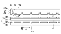
우선, 도 10에 도시한 바와 같이, 제1 대상 기판(110A) 위에 제1 스위칭 트랜지스터(T1) 및 제1 구동 트랜지스터(T2)를 형성하고, 제1 스위칭 트랜지스터(T1) 및 제1 구동 트랜지스터(T2)를 덮는 보호막(180)을 형성한다. 그리고, 제1 구동 트랜지스터(T2)에 연결되는 제1 화소 전극(190A)을 형성한다. 그리고, 제1 화소 전극(190A)의 가장자리와 보호막(180)을 덮는 화소 정의막(350)을 형성한다. 10, a first switching transistor T1 and a first driving transistor T2 are formed on a
다음으로, 제1 화소 전극(190A) 위에 제1 유기 발광층(270A)을 형성한다. 제1 유기 발광층(270A)을 형성하는 단계는 상기 제1 유기막 패턴(50A)을 형성하는 단계와 대부분 동일하다. Next, a first
즉, 도 11에 도시한 바와 같이, 유기막 패턴 형성용 마스크(1)의 도너 기판(20)의 흡수막(22) 위에 유기막(23)을 도포한다. 그리고, 제1 유기 발광층(270A)을 형성할 제1 대상 기판(110A)을 유기막 패턴 형성용 마스크(1)와 대향시켜 정렬한다. 그리고, 광원(30)을 유기막 패턴 형성용 마스크(1)의 포토 마스크(10)의 배면에 위치시키고 빛을 조사한다. 그러면, 반사부(A1)에 위치한 반사막(12)에 조사된 빛은 반사되고, 집광부(A2)에 위치하는 집광 패턴(11a)에 조사된 빛만이 집광되어 도너 기판(20)의 흡수막(22)에 포커싱된다. 따라서, 포커싱된 빛 에너지는 열 에너지로 변환되어 흡수막(22)을 가열시키므로, 유기막(23) 중 흡수막(22) 위 또는 그 주위에 위치한 전사 유기막(23a)도 가열된다.11, the
이에 따라, 도 12에 도시한 바와 같이, 유기막(23) 중 전사 유기막(23a)은 가열 및 승화되어 제1 대상 기판(110A)으로 전사되므로 제1 대상 기판(110A)에 제1 유기 발광층(270A)이 형성된다. 12, the transfer
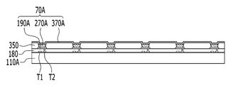
다음으로, 도 13에 도시한 바와 같이, 제1 유기 발광층(270A) 위에 제1 공통 전극(370A)을 형성하여, 제1 화소 전극(190A), 제1 유기 발광층(270A) 및 제1 공통 전극(370A)을 포함하는 제1 유기 발광 다이오드(70A)를 완성한다. Next, as shown in FIG. 13, a first
다음으로, 도 14에 도시한 바와 같이, 포토 마스크(10)를 수평 방향(X)으로 이동시켜 포토 마스크(10)의 집광부(A2)와 도너 기판(20)의 유기막(23) 중 미전사된 미전사 유기막(23b)을 중첩시킨다. 그리고, 제2 유기 발광층(270B)을 형성할 제2 대상 기판(110B)을 유기막 패턴 형성용 마스크(1)와 대향시켜 정렬한다. 제2 대상 기판(110B)에는 제2 스위칭 트랜지스터(T3) 및 제2 구동 트랜지스터(T4)를 형성하고, 제2 스위칭 트랜지스터(T3) 및 제2 구동 트랜지스터(T4)를 덮는 보호막(180)을 형성한다. 그리고, 제2 구동 트랜지스터(T4)에 연결되는 제2 화소 전극(190B)을 형성한다. 그리고, 제1 화소 전극(190A)의 가장자리와 보호막(180)을 덮는 화소 정의막(350)을 형성한다. 14, the
그리고, 광원(30)을 유기막 패턴 형성용 마스크(1)의 포토 마스크(10)의 배면에 위치시키고 빛을 조사한다. 그러면, 반사부(A1)에 위치한 반사막(12)에 조사된 빛은 반사되고, 집광부(A2)에 위치하는 집광 패턴(11a)에 조사된 빛은 집광되어 도너 기판(20)의 흡수막(22)에 포커싱된다. 따라서, 포커싱된 빛 에너지는 열 에너지로 변환되어 흡수막(22)을 가열시키므로, 유기막(23) 중 흡수막(22) 위 또는 그 주위에 위치한 미전사 유기막(23b)도 가열된다.Then, the
이에 따라, 도 15에 도시한 바와 같이, 유기막(23) 중 미전사 유기막(23b)은 승화되어 제2 대상 기판(110B)으로 전사되므로 제2 대상 기판(110B)에 제2 유기 발광층(270B)이 형성된다.15, the non-transferred
이와 같이, 유기막이 형성된 한 장의 도너 기판을 이용하여 적어도 하나 이상의 대상 기판에 유기 발광층을 형성할 수 있으므로, 유기막 패턴 형성용 마스크의 활용율을 높이고, 유기막 재료의 사용량을 증가시킬 수 있다. As described above, since the organic light emitting layer can be formed on at least one target substrate using a single donor substrate on which the organic film is formed, the utilization rate of the organic film pattern forming mask can be increased and the amount of the organic film material used can be increased.
그리고, 도 16에 도시한 바와 같이, 제2 유기 발광층(270B) 위에 제2 공통 전극(370B)을 형성하여, 제2 화소 전극(190B), 제2 유기 발광층(270B) 및 제2 공통 전극(370B)을 포함하는 제2 유기 발광 다이오드(70B)를 완성한다.16, a second
상기에서는 본 발명의 바람직한 실시예에 대하여 설명하였지만, 본 발명은 이에 한정되는 것이 아니고 특허청구범위와 발명의 상세한 설명 및 첨부한 도면의 범위 안에서 여러 가지로 변형하여 실시하는 것이 가능하고 이 또한 본 발명의 범위에 속하는 것은 당연하다.While the present invention has been described in connection with what is presently considered to be practical exemplary embodiments, it is to be understood that the invention is not limited to the disclosed embodiments, but, on the contrary, Of course.
1: 유기막 패턴 형성용 마스크
10: 포토 마스크
11: 제1 기판
11a: 집광 패턴
12: 반사막
20: 도너 기판
21: 제2 기판
22: 흡수막
23: 유기막
30: 광원
50A: 제1 유기막 패턴
50B: 제2 유기막 패턴1: mask for forming organic film pattern 10: photomask
11:
12: reflective film 20: donor substrate
21: second substrate 22: absorbing film
23: organic film 30: light source
50A: first
Claims (24)
상기 포토 마스크와 이격되어 상부에 위치하고 있으며 제2 기판, 상기 제2 기판 위에 형성되는 흡수막을 포함하는 도너 기판
을 포함하고,
상기 포토 마스크는 상기 포토 마스크에 입사한 빛을 반사시키는 반사부, 상기 빛을 집광시켜 상기 도너 기판으로 전달하는 집광부를 포함하는 유기막 패턴 형성용 마스크.A first substrate, a photomask including a reflective film formed on the first substrate,
A second substrate, and an absorptive film formed on the second substrate, the donor substrate being spaced apart from the photomask,
/ RTI >
Wherein the photomask includes a reflective portion that reflects light incident on the photomask, and a condenser that condenses the light and transmits the condensed light to the donor substrate.
상기 반사부와 상기 집광부는 서로 교대로 배치되어 있는 유기막 패턴 형성용 마스크.The method of claim 1,
Wherein the reflective portion and the light condensing portion are alternately arranged.
상기 제1 기판의 표면 중 상기 집광부에는 복수개의 집광 패턴이 형성되어 있는 유기막 패턴 형성용 마스크.The method of claim 1,
Wherein a plurality of light condensing patterns are formed on the light collecting portion of the surface of the first substrate.
상기 집광 패턴은 음각 형상인 유기막 패턴 형성용 마스크.4. The method of claim 3,
Wherein the light converging pattern is a concave shape.
상기 음각 형상은 오목한 반원 형상의 단면을 가지는 유기막 패턴 형성용 마스크.5. The method of claim 4,
Wherein the concave shape has a concave semicircular cross section.
상기 음각 형상은 볼록한 반원 형상의 단면을 가지는 유기막 패턴 형성용 마스크.5. The method of claim 4,
Wherein the concave shape has a convex semi-circular cross section.
상기 음각 형상은 오목한 삼각 형상의 단면을 가지는 유기막 패턴 형성용 마스크.5. The method of claim 4,
Wherein the depressed shape has a concave triangular cross section.
상기 집광 패턴은 양각 형상인 유기막 패턴 형성용 마스크.4. The method of claim 3,
Wherein the light converging pattern is a concave shape.
상기 양각 형상은 볼록한 반원 형상의 단면을 가지는 유기막 패턴 형성용 마스크.9. The method of claim 8,
Wherein the embossed shape has a convex semicircular cross section.
상기 반사막은 상기 반사부에 형성되어 있는 유기막 패턴 형성용 마스크.4. The method of claim 3,
Wherein the reflective film is formed on the reflective portion.
상기 유기막 패턴 형성용 마스크와 제1 대상 기판을 서로 정렬하는 단계,
상기 유기막 패턴 형성용 마스크의 배면에 빛을 조사하여 상기 흡수막을 가열시켜 상기 제1 대상 기판에 제1 유기막 패턴을 형성하는 단계
를 포함하는 유기막 패턴 형성 방법.A step of applying an organic film on an absorption layer of a mask for forming an organic film pattern including a photomask including a reflective film, a donor substrate spaced apart from the photomask and having an absorption layer,
Aligning the mask for forming an organic film pattern and a first object substrate with each other,
Forming a first organic film pattern on the first target substrate by irradiating light on a back surface of the mask for forming an organic film pattern to heat the absorbing film;
Wherein the organic film pattern is formed on the substrate.
상기 포토 마스크는 상기 포토 마스크에 입사한 빛을 반사시키는 반사부, 상기 빛을 집광시켜 상기 도너 기판으로 전달하는 집광부를 포함하는 유기막 패턴 형성 방법.12. The method of claim 11,
Wherein the photomask includes a reflector that reflects light incident on the photomask, and a condenser that condenses the light and transmits the condensed light to the donor substrate.
상기 반사부와 상기 집광부는 서로 교대로 배치되어 있는 유기막 패턴 형성방법.The method of claim 12,
Wherein the reflection portion and the light condensing portion are alternately arranged.
상기 유기막 중 상기 집광부에 대응하는 위치에 형성된 전사 유기막은 상기 제1 대상 기판으로 전사되어 제1 유기막 패턴을 형성하는 유기막 패턴 형성 방법.The method of claim 13,
Wherein a transfer organic film formed at a position corresponding to the light collecting portion of the organic film is transferred to the first substrate to form a first organic film pattern.
상기 포토 마스크를 이동시켜 상기 포토 마스크의 집광부와 상기 도너 기판의 유기막 중 미전사된 미전사 유기막을 중첩시키는 단계,
상기 유기막 패턴 형성용 마스크와 제2 대상 기판을 서로 정렬하는 단계,
상기 유기막 패턴 형성용 마스크의 배면에 빛을 조사하여 상기 흡수막을 가열시켜 상기 제2 대상 기판에 제2 유기막 패턴을 형성하는 단계
를 더 포함하는 유기막 패턴 형성 방법.The method of claim 14,
Moving the photomask to overlap a non-transferred organic film in the organic film of the donor substrate and the light collecting part of the photomask,
Aligning the organic film pattern forming mask and the second target substrate with each other,
Forming a second organic film pattern on the second target substrate by irradiating light on a back surface of the mask for forming an organic film pattern to heat the absorbing film
Further comprising a step of forming an organic film pattern.
상기 미전사 유기막은 상기 제2 대상 기판으로 전사되어 제2 유기막 패턴을 형성하는 유기막 패턴 형성 방법.16. The method of claim 15,
Wherein the non-transferred organic film is transferred to the second target substrate to form a second organic film pattern.
상기 집광부에는 복수개의 집광 패턴이 형성되어 있는 유기막 패턴 형성 방법.The method of claim 12,
And a plurality of condensing patterns are formed in the light collecting portion.
상기 제1 구동 트랜지스터에 연결되는 제1 화소 전극을 형성하는 단계,
상기 제1 화소 전극 위에 제1 유기 발광층을 형성하는 단계,
상기 제1 유기 발광층 위에 제1 공통 전극을 형성하는 단계를 포함하고,
상기 제1 유기 발광층을 형성하는 단계는
반사막을 포함하는 포토 마스크, 상기 포토 마스크와 이격되어 상부에 위치하고 있으며 흡수막을 포함하는 도너 기판을 포함하는 유기막 패턴 형성용 마스크 의 흡수막 위에 유기막을 도포하는 단계,
상기 유기막 패턴 형성용 마스크와 상기 제1 화소 전극이 형성된 제1 대상 기판을 서로 정렬하는 단계,
상기 유기막 패턴 형성용 마스크의 배면에 빛을 조사하여 상기 흡수막을 가열시켜 상기 제1 대상 기판의 제1 화소 전극 위에 제1 유기 발광층을 형성하는 단계
를 포함하는 유기 발광 표시 장치의 제조 방법.Forming a first switching transistor and a first driving transistor on a first substrate,
Forming a first pixel electrode connected to the first driving transistor,
Forming a first organic light emitting layer on the first pixel electrode,
Forming a first common electrode on the first organic light emitting layer,
The step of forming the first organic light emitting layer
A step of applying an organic film on an absorbing film of a mask for forming an organic film pattern including a photomask including a reflective film, a donor substrate spaced apart from the photomask and including an absorbing film,
Aligning the mask for forming an organic film pattern and a first object substrate on which the first pixel electrode is formed,
Forming a first organic light emitting layer on the first pixel electrode of the first substrate by irradiating light on the back surface of the mask for forming an organic film pattern and heating the absorbing film
Wherein the organic light emitting display device further comprises:
상기 포토 마스크는 상기 포토 마스크에 입사한 빛을 반사시키는 반사부, 상기 빛을 집광시켜 상기 도너 기판으로 전달하는 집광부를 포함하는 유기 발광 표시 장치의 제조 방법.The method of claim 18,
Wherein the photomask includes a reflective portion that reflects light incident on the photomask, and a condenser that condenses the light and transmits the condensed light to the donor substrate.
상기 반사부와 상기 집광부는 서로 교대로 배치되어 있는 유기 발광 표시 장치의 제조 방법.20. The method of claim 19,
Wherein the reflective portion and the light-converging portion are alternately arranged.
상기 유기막 중 상기 집광부에 대응하는 위치에 형성된 전사 유기막은 상기 제1 대상 기판으로 전사되어 제1 유기 발광층을 형성하는 유기 발광 표시 장치의 제조 방법.20. The method of claim 20,
Wherein a transfer organic film formed at a position corresponding to the light collecting portion of the organic film is transferred to the first substrate to form a first organic light emitting layer.
제2 대상 기판 위에 제2 스위칭 트랜지스터 및 제2 구동 트랜지스터를 형성하는 단계,
상기 제2 구동 트랜지스터에 연결되는 제2 화소 전극을 형성하는 단계,
상기 제2 화소 전극 위에 제2 유기 발광층을 형성하는 단계,
상기 제2 유기 발광층 위에 제2 공통 전극을 형성하는 단계를 더 포함하고,
상기 제2 유기 발광층을 형성하는 단계는
상기 포토 마스크를 이동시켜 상기 포토 마스크의 집광부와 상기 도너 기판의 유기막 중 미전사된 미전사 유기막을 중첩시키는 단계,
상기 유기막 패턴 형성용 마스크와 상기 제2 화소 전극이 형성된 제2 대상 기판을 서로 정렬하는 단계,
상기 유기막 패턴 형성용 마스크의 배면에 빛을 조사하여 상기 흡수막을 가열시켜 상기 제2 대상 기판의 제2 화소 전극 위에 제2 유기 발광층을 형성하는 단계
를 더 포함하는 유기 발광 표시 장치의 제조 방법.22. The method of claim 21,
Forming a second switching transistor and a second driving transistor on a second substrate,
Forming a second pixel electrode connected to the second driving transistor,
Forming a second organic emission layer on the second pixel electrode,
Forming a second common electrode on the second organic light emitting layer,
The step of forming the second organic light emitting layer
Moving the photomask to overlap a non-transferred organic film in the organic film of the donor substrate and the light collecting part of the photomask,
Aligning the mask for forming an organic film pattern and a second object substrate on which the second pixel electrode is formed,
Forming a second organic light emitting layer on the second pixel electrode of the second substrate by irradiating light on the back surface of the mask for forming an organic film pattern and heating the absorbing film
Further comprising the steps of:
상기 미전사 유기막은 상기 제2 대상 기판으로 전사되어 제2 유기 발광층을 형성하는 유기 발광 표시 장치의 제조 방법.The method of claim 22,
Wherein the non-transferred organic film is transferred to the second target substrate to form a second organic light emitting layer.
상기 집광부에는 복수개의 집광 패턴이 형성되어 있는 유기 발광 표시 장치의 제조 방법.24. The method of claim 23,
And a plurality of light converging patterns are formed in the light collecting portion.
Priority Applications (5)
| Application Number | Priority Date | Filing Date | Title |
|---|---|---|---|
| KR1020140031857A KR20150109013A (en) | 2014-03-18 | 2014-03-18 | Mask for forming organic layer pattern, forming method of organic layer pattern and manufacturing method of organic light emitting diode display using the same |
| US14/532,993 US9583709B2 (en) | 2014-03-18 | 2014-11-04 | Mask for forming organic layer pattern, forming method of organic layer pattern, and manufacturing method of organic light emitting diode display using the same |
| EP14196461.9A EP2922108A1 (en) | 2014-03-18 | 2014-12-05 | Mask for forming organic layer pattern, forming method of organic layer pattern, and manufacturing method of organic light emitting diode display using the same |
| JP2015008448A JP2015179663A (en) | 2014-03-18 | 2015-01-20 | Mask for forming organic film pattern, and organic film pattern forming method and organic light emitting display manufacturing method using the mask |
| CN201510030677.4A CN104934370A (en) | 2014-03-18 | 2015-01-21 | Mask, forming method of organic layer pattern, and manufacturing method of display |
Applications Claiming Priority (1)
| Application Number | Priority Date | Filing Date | Title |
|---|---|---|---|
| KR1020140031857A KR20150109013A (en) | 2014-03-18 | 2014-03-18 | Mask for forming organic layer pattern, forming method of organic layer pattern and manufacturing method of organic light emitting diode display using the same |
Publications (1)
| Publication Number | Publication Date |
|---|---|
| KR20150109013A true KR20150109013A (en) | 2015-10-01 |
Family
ID=52003652
Family Applications (1)
| Application Number | Title | Priority Date | Filing Date |
|---|---|---|---|
| KR1020140031857A KR20150109013A (en) | 2014-03-18 | 2014-03-18 | Mask for forming organic layer pattern, forming method of organic layer pattern and manufacturing method of organic light emitting diode display using the same |
Country Status (5)
| Country | Link |
|---|---|
| US (1) | US9583709B2 (en) |
| EP (1) | EP2922108A1 (en) |
| JP (1) | JP2015179663A (en) |
| KR (1) | KR20150109013A (en) |
| CN (1) | CN104934370A (en) |
Families Citing this family (5)
| Publication number | Priority date | Publication date | Assignee | Title |
|---|---|---|---|---|
| DE102015101932A1 (en) * | 2015-02-11 | 2016-08-25 | Von Ardenne Gmbh | Method and device for the structured coating of substrates |
| WO2019113852A1 (en) * | 2017-12-13 | 2019-06-20 | 深圳市柔宇科技有限公司 | Mask used for vacuum vapor deposition, vapor deposition method, display apparatus, and vapor deposition device |
| KR20220056914A (en) * | 2020-10-28 | 2022-05-09 | 삼성디스플레이 주식회사 | Mask frame and deposition apparatus including the same |
| KR102338064B1 (en) * | 2021-06-11 | 2021-12-13 | 주식회사 올레드링크 | OLED Panel Manufacturing Method |
| KR102337855B1 (en) * | 2021-09-03 | 2021-12-13 | 주식회사 올레드링크 | OLED Panel with Improved Deposition Effect |
Family Cites Families (20)
| Publication number | Priority date | Publication date | Assignee | Title |
|---|---|---|---|---|
| US6610455B1 (en) * | 2002-01-30 | 2003-08-26 | Eastman Kodak Company | Making electroluminscent display devices |
| JP4230187B2 (en) * | 2002-09-25 | 2009-02-25 | シャープ株式会社 | Microlens array manufacturing method and microlens array manufacturing apparatus |
| WO2004114001A1 (en) * | 2003-06-20 | 2004-12-29 | Casio Computer Co., Ltd. | Display device and manufacturing method of the same |
| WO2005093466A1 (en) * | 2004-03-26 | 2005-10-06 | Sony Corporation | Microlens array substrate and production method therefor |
| KR100635569B1 (en) | 2004-09-23 | 2006-10-17 | 삼성에스디아이 주식회사 | laser irradiation device and fabrication method of organic electroluminescence display device using the same |
| KR100782470B1 (en) | 2006-05-22 | 2007-12-05 | 삼성에스디아이 주식회사 | laser irradiation device and fabrication method of organic light emitting display device using the same |
| US7994021B2 (en) * | 2006-07-28 | 2011-08-09 | Semiconductor Energy Laboratory Co., Ltd. | Method of manufacturing semiconductor device |
| JP2008089926A (en) * | 2006-09-29 | 2008-04-17 | Oki Electric Ind Co Ltd | Microoptical element, manufacture method therefor, and photomask |
| KR20090028413A (en) * | 2007-09-13 | 2009-03-18 | 가부시키가이샤 한도오따이 에네루기 켄큐쇼 | Manufacturing method of light emitting device, and evaporation donor substrate |
| US8153201B2 (en) * | 2007-10-23 | 2012-04-10 | Semiconductor Energy Laboratory Co., Ltd. | Method of manufacturing light-emitting device, and evaporation donor substrate |
| US8425974B2 (en) | 2007-11-29 | 2013-04-23 | Semiconductor Energy Laboratory Co., Ltd. | Evaporation donor substrate and method for manufacturing light-emitting device |
| KR101689519B1 (en) * | 2007-12-26 | 2016-12-26 | 가부시키가이샤 한도오따이 에네루기 켄큐쇼 | Evaporation donor substrate, method for manufacturing the same, and method for manufacturing light-emitting device |
| WO2009128164A1 (en) * | 2008-04-17 | 2009-10-22 | 凸版印刷株式会社 | Optical device, uniform illumination device, optical sheet, backlight unit, and display unit |
| US8409672B2 (en) * | 2008-04-24 | 2013-04-02 | Semiconductor Energy Laboratory Co., Ltd. | Method of manufacturing evaporation donor substrate and method of manufacturing light-emitting device |
| US8405909B2 (en) * | 2008-05-09 | 2013-03-26 | Semiconductor Energy Laboratories Co., Ltd. | Deposition donor substrate and deposition method using the same |
| US8574709B2 (en) * | 2008-07-21 | 2013-11-05 | Semiconductor Energy Laboratory Co., Ltd. | Deposition donor substrate and method for manufacturing light-emitting device |
| JP2010093068A (en) | 2008-10-08 | 2010-04-22 | Hitachi Displays Ltd | Organic el display device and method of manufacturing the same |
| US20100123260A1 (en) * | 2008-11-19 | 2010-05-20 | Jacques Duparre | Stamp with mask pattern for discrete lens replication |
| JP5291607B2 (en) | 2008-12-15 | 2013-09-18 | 株式会社半導体エネルギー研究所 | Method for manufacturing light emitting device |
| KR101813548B1 (en) | 2011-06-30 | 2018-01-02 | 삼성디스플레이 주식회사 | Laser induced thermal imaging apparatus and method for manufacturing organic light emitting display device using the same |
-
2014
- 2014-03-18 KR KR1020140031857A patent/KR20150109013A/en not_active Application Discontinuation
- 2014-11-04 US US14/532,993 patent/US9583709B2/en not_active Expired - Fee Related
- 2014-12-05 EP EP14196461.9A patent/EP2922108A1/en not_active Withdrawn
-
2015
- 2015-01-20 JP JP2015008448A patent/JP2015179663A/en active Pending
- 2015-01-21 CN CN201510030677.4A patent/CN104934370A/en active Pending
Also Published As
| Publication number | Publication date |
|---|---|
| US9583709B2 (en) | 2017-02-28 |
| US20150270486A1 (en) | 2015-09-24 |
| CN104934370A (en) | 2015-09-23 |
| JP2015179663A (en) | 2015-10-08 |
| EP2922108A1 (en) | 2015-09-23 |
Similar Documents
| Publication | Publication Date | Title |
|---|---|---|
| JP6595049B2 (en) | Vapor deposition mask, mask member for vapor deposition mask, method for producing vapor deposition mask, and method for producing organic EL display device | |
| KR20150109013A (en) | Mask for forming organic layer pattern, forming method of organic layer pattern and manufacturing method of organic light emitting diode display using the same | |
| CN1769066B (en) | Donor substrate and fabrication method of organic light emitting display using the same | |
| TWI321822B (en) | Transfer substrate, transfer method, and method of manufacturing display device | |
| KR102097443B1 (en) | Organic luminescence display and method for manufacturing the same | |
| KR100700654B1 (en) | Laser Irradiation Device and Laser Induced Thermal Imaging | |
| JP2009123692A5 (en) | ||
| US9130194B2 (en) | Donor substrate for transfer and manufacturing method of organic light emitting diode display | |
| JP5685350B2 (en) | TRANSFER MASK FOR DEPOSITION ON A SPECIFIC LOCATION OF A SUBSTRATE AND METHOD FOR PRODUCING THE TRANSFER MASK | |
| KR20150056112A (en) | Mask for forming layer, forming method of layer and manufacturing method of organic light emitting diode display using the same | |
| TW201445731A (en) | Organic light emitting display device | |
| JP2007511889A (en) | Method for manufacturing electroluminescent device including color filter | |
| US9180715B2 (en) | Donor film and thermal imaging method using the same | |
| KR20160018925A (en) | Optical mask and laser transfer method using the same | |
| KR102180647B1 (en) | Optical mask | |
| TW201438318A (en) | Donor substrate and method of forming transfer pattern using the same | |
| KR101887082B1 (en) | Organic light emitting diode device and fabrication method thereof | |
| JP6071164B2 (en) | Laser thermal transfer mask and organic electroluminescence display device manufacturing method using the same | |
| KR20160034529A (en) | Optical pattern transfer mask and method for fabricating the same | |
| KR102144855B1 (en) | Optical mask | |
| KR20160046169A (en) | Optical mask | |
| JP2010267410A (en) | Donor substrate used for transferring method using laser, and manufacturing method of display element | |
| KR20140074773A (en) | Organic optical mask, apparatus for irradiating laser having the same and method for fabricationg organic light emitting dioide device using the same | |
| US9349956B2 (en) | Laminating apparatus and method of manufacturing organic light-emitting display using the same | |
| KR102468454B1 (en) | Transparent solar cell and fabrication method of the same |
Legal Events
| Date | Code | Title | Description |
|---|---|---|---|
| WITN | Application deemed withdrawn, e.g. because no request for examination was filed or no examination fee was paid |