JP5281069B2 - 集積回路 - Google Patents
集積回路 Download PDFInfo
- Publication number
- JP5281069B2 JP5281069B2 JP2010271209A JP2010271209A JP5281069B2 JP 5281069 B2 JP5281069 B2 JP 5281069B2 JP 2010271209 A JP2010271209 A JP 2010271209A JP 2010271209 A JP2010271209 A JP 2010271209A JP 5281069 B2 JP5281069 B2 JP 5281069B2
- Authority
- JP
- Japan
- Prior art keywords
- fin
- transistor
- straight
- straight fin
- integrated circuit
- Prior art date
- Legal status (The legal status is an assumption and is not a legal conclusion. Google has not performed a legal analysis and makes no representation as to the accuracy of the status listed.)
- Active
Links
Images
Classifications
-
- H—ELECTRICITY
- H10—SEMICONDUCTOR DEVICES; ELECTRIC SOLID-STATE DEVICES NOT OTHERWISE PROVIDED FOR
- H10B—ELECTRONIC MEMORY DEVICES
- H10B10/00—Static random access memory [SRAM] devices
- H10B10/12—Static random access memory [SRAM] devices comprising a MOSFET load element
-
- H—ELECTRICITY
- H10—SEMICONDUCTOR DEVICES; ELECTRIC SOLID-STATE DEVICES NOT OTHERWISE PROVIDED FOR
- H10B—ELECTRONIC MEMORY DEVICES
- H10B10/00—Static random access memory [SRAM] devices
-
- H—ELECTRICITY
- H10—SEMICONDUCTOR DEVICES; ELECTRIC SOLID-STATE DEVICES NOT OTHERWISE PROVIDED FOR
- H10D—INORGANIC ELECTRIC SEMICONDUCTOR DEVICES
- H10D30/00—Field-effect transistors [FET]
- H10D30/60—Insulated-gate field-effect transistors [IGFET]
- H10D30/62—Fin field-effect transistors [FinFET]
- H10D30/6219—Fin field-effect transistors [FinFET] characterised by the source or drain electrodes
-
- H—ELECTRICITY
- H10—SEMICONDUCTOR DEVICES; ELECTRIC SOLID-STATE DEVICES NOT OTHERWISE PROVIDED FOR
- H10D—INORGANIC ELECTRIC SEMICONDUCTOR DEVICES
- H10D89/00—Aspects of integrated devices not covered by groups H10D84/00 - H10D88/00
- H10D89/10—Integrated device layouts
Landscapes
- Semiconductor Memories (AREA)
- Metal-Oxide And Bipolar Metal-Oxide Semiconductor Integrated Circuits (AREA)
Description
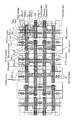
BL-contact、BLB-contact コンタクト
Cut-gate 切断ゲート
Dummy1、Dummy2 ダミートランジスタ
Dummy1-SD ダミートランジスタのソース/ドレイン領域
Fin1、Fin2、Fin2-1〜Fin2-3、Fin2-3’、Fin3、Fin4、Fin5 フィン
Fin-End 後端キャップ
G1、G2 ゲートストリップ
M1-connect 金属線
PD1、PD2 プルダウントランジスタ
PD-11、PD-12、PD-13、PD-21、PD-22 サブプルダウントランジスタ
PG1、PG2 パスゲートトランジスタ
PG-11、PG-12、PG-21、PG-22 サブパスゲートトランジスタ
PU1、PU2 プルアップトランジスタ
PU-11、PU-12、PU-21、PU-22 サブトランジスタ
VCC 正の電源ノード
VCC-contact、VSS-contact、Butted-contact、PD-D、VSS-contact1、VSS-contact2 コンタクト
VSS 電源ノード
S1、S2、S3 距離
WL ワードライン
Claims (10)
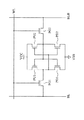
- 集積回路構造であって、SRAMセルからなり、前記SRAMセルは、
第一ストレート(straight)フィンと、
前記第一ストレートフィンから物理的に切り離され、前記第一ストレートフィンに平行な第一部分と第二部分を有する屈曲(bended)フィンと、
前記第一ストレートフィンに平行でなく、前記第一部分と前記第二部分に相互接続される前記屈曲フィンの第三部分と、
第一ゲートストリップの部分を含み、前記第一ゲートストリップが、前記第一ストレートフィンと前記屈曲フィンの前記第一部分を有する第一、及び、第二サブプルダウントランジスタを形成するプルダウントランジスタと、
第二ゲートストリップの部分を含み、前記第二ゲートストリップが、前記第一ストレートフィンを有する第一サブパスゲートトランジスタを形成するパスゲートトランジスタと、
を含み、
前記屈曲フィンの前記第一部分と前記第一ストレートフィンは第一距離を有し、前記屈曲フィンの前記第二部分と前記第一ストレートフィンは、前記第一距離より大きい第二距離を有し、
前記プルダウントランジスタのフィンの第一の数は、前記パスゲートトランジスタのフィンの第二の数より多いことを特徴とする集積回路。 - 更に、前記第一ストレートフィンに平行な第二ストレートフィンを有し、前記プルダウントランジスタは、更に、前記第二ストレートフィンの第一部分からなる第三サブプルダウントランジスタを含み、前記パスゲートトランジスタは、更に、前記第二ストレートフィンの第二部分からなる第二サブパスゲートトランジスタを含むことを特徴とする請求項1に記載の集積回路。
- 前記第一距離は、前記集積回路の形成技術により許容される最小距離にほぼ等しく、前記集積回路は、更に、
前記第一ストレートフィンの一部上の第一エピタキシャル半導体領域と、
前記屈曲フィンの前記第一部分上にあり、且つ、前記第一エピタキシャル半導体領域と、連続した半導体領域を形成する第二エピタキシャル半導体領域と、
前記第一ストレートフィンと前記屈曲フィン間に水平に位置し、前記第一、及び、前記第二エピタキシャル半導体領域に電気的に接続されるコンタクトプラグと、
からなることを特徴とする請求項1に記載の集積回路。 - 前記第一距離は、前記集積回路の形成技術により許容される最小距離にほぼ等しく、前記集積回路構造は、更に、前記第一ストレートフィンと前記屈曲フィン上に直接延伸し、電気的に接続されるコンタクトプラグを有することを特徴とする請求項1に記載の集積回路。
- 前記屈曲フィンの前記第二部分は、前記SRAMセルの境界まで延伸し、前記第二ゲートストリップを有するダミートランジスタを形成し、前記屈曲フィンの前記第二部分は、追加のSRAMセル中の追加のダミートランジスタの追加フィンと、連続した半導体フィンを形成することを特徴とする請求項1に記載の集積回路。
- 集積回路構造であって、SRAMセルからなり、前記SRAMセルは、
第一ストレートフィンと、屈曲フィンとを有し、
前記屈曲フィンは、前記第一ストレートフィンに平行な第一部分と、前記第一ストレートフィンに平行な第二部分と、前記第一ストレートフィンに平行でなく、前記第一部分と前記第二部分と相互接続される前記屈曲フィンの第三部分を有すると共に、
第一ゲートストリップの部分を含み、前記第一ゲートストリップが、前記第一ストレートフィンと前記屈曲フィンの前記第一部分を有する第一、及び、第二サブプルダウントランジスタを形成するプルダウントランジスタと、
第二ゲートストリップの部分を含み、前記第二ゲートストリップが、前記第一ストレートフィンを有する第一サブパスゲートトランジスタを形成すると共に、前記屈曲フィンの前記第二部分を有するダミートランジスタを形成し、前記第一サブパスゲートトランジスタと前記ダミートランジスタによって構成されたパスゲートトランジスタと備え、
前記屈曲フィンの前記第一部分と前記第一ストレートフィンは第一距離を有し、前記屈曲フィンの前記第二部分と前記第一ストレートフィンは、前記第一距離より大きい第二距離を有することを特徴とする集積回路構造。 - 更に、第二ストレートフィンを有し、
前記プルダウントランジスタは、更に、前記第二ストレートフィンの第一部分と前記第一ゲートストリップの追加部分とを含む第三サブプルダウントランジスタを含み、
前記パスゲートトランジスタは、更に、前記第二ストレートフィンの第二部分と、前記第二ゲートストリップの追加部分を含む第二サブパスゲートトランジスタを含むことを特徴とする請求項6に記載の集積回路構造。 - 前記屈曲フィンの前記第二部分は前記SRAMセルの境界まで延伸し、追加のSRAMセルの追加のダミートランジスタの追加のフィンと、連続した半導体フィンを形成することを特徴とする請求項6に記載の集積回路構造。
- 集積回路構造であって、SRAMセルからなり、前記SRAMセルは、
第一ストレートフィンと、
前記第一ストレートフィンから物理的に切り離され、前記第一ストレートフィンに平行な第二ストレートフィンと、
第一ゲートストリップの部分を含み、前記第一ゲートストリップが、前記第一ストレートフィンの第一部分及び前記第二ストレートフィンの第一部分をそれぞれ備えた第一、及び、第二サブプルダウントランジスタを形成するプルダウントランジスタと、
第二ゲートストリップの部分を含み、前記第二ゲートストリップが、前記第一ストレートフィンの第二部分を有するパスゲートトランジスタの第一サブパスゲートトランジスタを形成すると共に、前記第二ゲートストリップが、前記第二ストレートフィンの第二部分に直接延伸し、ダミートランジスタを形成するパスゲートトランジスタと、
からなることを特徴とする集積回路構造。 - 前記第二ストレートフィンは前記SRAMセルの境界まで延伸し、追加のSRAMセル中の追加のダミートランジスタの追加のフィンと、連続した半導体フィンを形成することを特徴とする請求項9に記載の集積回路構造。
Applications Claiming Priority (4)
| Application Number | Priority Date | Filing Date | Title |
|---|---|---|---|
| US26734109P | 2009-12-07 | 2009-12-07 | |
| US61/267,341 | 2009-12-07 | ||
| US12/890,132 | 2010-09-24 | ||
| US12/890,132 US8258572B2 (en) | 2009-12-07 | 2010-09-24 | SRAM structure with FinFETs having multiple fins |
Publications (2)
| Publication Number | Publication Date |
|---|---|
| JP2011119741A JP2011119741A (ja) | 2011-06-16 |
| JP5281069B2 true JP5281069B2 (ja) | 2013-09-04 |
Family
ID=44081196
Family Applications (1)
| Application Number | Title | Priority Date | Filing Date |
|---|---|---|---|
| JP2010271209A Active JP5281069B2 (ja) | 2009-12-07 | 2010-12-06 | 集積回路 |
Country Status (6)
| Country | Link |
|---|---|
| US (2) | US8258572B2 (ja) |
| JP (1) | JP5281069B2 (ja) |
| KR (1) | KR101212368B1 (ja) |
| CN (1) | CN102122660B (ja) |
| DE (2) | DE102010053571B4 (ja) |
| TW (1) | TWI474471B (ja) |
Families Citing this family (63)
| Publication number | Priority date | Publication date | Assignee | Title |
|---|---|---|---|---|
| US8399931B2 (en) | 2010-06-30 | 2013-03-19 | Taiwan Semiconductor Manufacturing Company, Ltd. | Layout for multiple-fin SRAM cell |
| US8675397B2 (en) | 2010-06-25 | 2014-03-18 | Taiwan Semiconductor Manufacturing Company, Ltd. | Cell structure for dual-port SRAM |
| JP2012064854A (ja) * | 2010-09-17 | 2012-03-29 | Toshiba Corp | 半導体装置 |
| US8561003B2 (en) | 2011-07-29 | 2013-10-15 | Synopsys, Inc. | N-channel and P-channel finFET cell architecture with inter-block insulator |
| US8595661B2 (en) * | 2011-07-29 | 2013-11-26 | Synopsys, Inc. | N-channel and p-channel finFET cell architecture |
| US8693235B2 (en) * | 2011-12-06 | 2014-04-08 | Taiwan Semiconductor Manufacturing Company, Ltd. | Methods and apparatus for finFET SRAM arrays in integrated circuits |
| US8802535B2 (en) * | 2012-05-02 | 2014-08-12 | International Business Machines Corporation | Doped core trigate FET structure and method |
| US9583398B2 (en) | 2012-06-29 | 2017-02-28 | Taiwan Semiconductor Manufacturing Company, Ltd. | Integrated circuit having FinFETS with different fin profiles |
| US9012287B2 (en) | 2012-11-14 | 2015-04-21 | Taiwan Semiconductor Manufacturing Company, Ltd. | Cell layout for SRAM FinFET transistors |
| US8779528B2 (en) * | 2012-11-30 | 2014-07-15 | Taiwan Semiconductor Manufacturing Company, Ltd. | SRAM cell comprising FinFETs |
| US8889561B2 (en) * | 2012-12-10 | 2014-11-18 | Globalfoundries Inc. | Double sidewall image transfer process |
| US9397217B2 (en) * | 2012-12-28 | 2016-07-19 | Taiwan Semiconductor Manufacturing Company, Ltd. | Contact structure of non-planar semiconductor device |
| US9812556B2 (en) | 2012-12-28 | 2017-11-07 | Renesas Electronics Corporation | Semiconductor device and method of manufacturing the semiconductor device |
| KR102049774B1 (ko) * | 2013-01-24 | 2019-11-28 | 삼성전자 주식회사 | 반도체 장치 및 그 제조 방법 |
| US8921191B2 (en) * | 2013-02-05 | 2014-12-30 | GlobalFoundries, Inc. | Integrated circuits including FINFET devices with lower contact resistance and reduced parasitic capacitance and methods for fabricating the same |
| US8796093B1 (en) * | 2013-03-14 | 2014-08-05 | International Business Machines Corporation | Doping of FinFET structures |
| JP6224818B2 (ja) * | 2013-03-30 | 2017-11-01 | インテル・コーポレーション | 集積回路および集積回路を形成する方法 |
| KR102072410B1 (ko) | 2013-08-07 | 2020-02-03 | 삼성전자 주식회사 | 반도체 장치 및 그 제조 방법 |
| CN105531813B (zh) * | 2013-09-04 | 2018-10-12 | 株式会社索思未来 | 半导体装置 |
| US9048123B2 (en) * | 2013-09-19 | 2015-06-02 | International Business Machines Corporation | Interdigitated finFETs |
| US9444460B1 (en) * | 2013-11-22 | 2016-09-13 | Altera Corporation | Integrated circuits with programmable overdrive capabilities |
| US9312273B2 (en) | 2013-12-02 | 2016-04-12 | International Business Machines Corporation | Structure and method to reduce crystal defects in epitaxial fin merge using nitride deposition |
| US9257439B2 (en) * | 2014-02-27 | 2016-02-09 | Taiwan Semiconductor Manufacturing Company, Ltd. | Structure and method for FinFET SRAM |
| US9224842B2 (en) * | 2014-04-22 | 2015-12-29 | Globalfoundries Inc. | Patterning multiple, dense features in a semiconductor device using a memorization layer |
| WO2015180595A1 (en) * | 2014-05-27 | 2015-12-03 | Mediatek Inc. | Fin field-effect transistor gated diode |
| US9852252B2 (en) | 2014-08-22 | 2017-12-26 | Samsung Electronics Co., Ltd. | Standard cell library and methods of using the same |
| US10242148B2 (en) * | 2014-08-25 | 2019-03-26 | Mediatek Inc. | Integrated circuit and routing design of the same |
| US9299706B1 (en) * | 2014-09-25 | 2016-03-29 | International Business Machines Corporation | Single source/drain epitaxy for co-integrating nFET semiconductor fins and pFET semiconductor fins |
| KR102288869B1 (ko) * | 2014-10-01 | 2021-08-10 | 삼성전자주식회사 | 시스템 온 칩 |
| US9418896B2 (en) | 2014-11-12 | 2016-08-16 | Samsung Electronics Co., Ltd. | Semiconductor device and fabricating method thereof |
| US9859286B2 (en) * | 2014-12-23 | 2018-01-02 | International Business Machines Corporation | Low-drive current FinFET structure for improving circuit density of ratioed logic in SRAM devices |
| KR102193633B1 (ko) * | 2014-12-30 | 2020-12-21 | 삼성전자주식회사 | 듀얼 포트 에스램 장치 및 그 제조 방법 |
| US9991384B2 (en) * | 2015-01-15 | 2018-06-05 | Taiwan Semiconductor Manufacturing Co., Ltd. | Semiconductor device including fin structures and manufacturing method thereof |
| KR102352153B1 (ko) | 2015-03-25 | 2022-01-17 | 삼성전자주식회사 | 집적회로 장치 및 이의 제조 방법 |
| KR102316119B1 (ko) * | 2015-04-02 | 2021-10-21 | 삼성전자주식회사 | 반도체 장치 |
| KR102170701B1 (ko) * | 2015-04-15 | 2020-10-27 | 삼성전자주식회사 | 반도체 장치 제조 방법 |
| US9391080B1 (en) * | 2015-04-28 | 2016-07-12 | Globalfoundries Inc. | Memory bit cell for reduced layout area |
| KR102400375B1 (ko) * | 2015-04-30 | 2022-05-20 | 삼성전자주식회사 | 반도체 장치 및 그 제조 방법 |
| KR20160136715A (ko) * | 2015-05-20 | 2016-11-30 | 삼성전자주식회사 | 반도체 장치 및 그 제조 방법 |
| US9922978B2 (en) * | 2015-08-21 | 2018-03-20 | Taiwan Semiconductor Manufacturing Co., Ltd | Semiconductor structure with recessed source/drain structure and method for forming the same |
| US9496269B1 (en) * | 2015-10-29 | 2016-11-15 | Taiwan Semiconductor Manufacturing Co., Ltd. | Static random access memory |
| US10121534B1 (en) * | 2015-12-18 | 2018-11-06 | Altera Corporation | Integrated circuit with overdriven and underdriven pass gates |
| US9455314B1 (en) | 2016-02-05 | 2016-09-27 | International Business Machines Corporation | Y-FET with self-aligned punch-through-stop (PTS) doping |
| CN106057900B (zh) * | 2016-06-17 | 2019-07-30 | 中国科学院微电子研究所 | 基于外延层的半导体器件及其制造方法及包括其的电子设备 |
| US10366196B2 (en) * | 2016-06-22 | 2019-07-30 | Qualcomm Incorporated | Standard cell architecture for diffusion based on fin count |
| US9892781B2 (en) | 2016-06-30 | 2018-02-13 | Taiwan Semiconductor Manufacturing Co., Ltd. | Cell structure for dual-port static random access memory |
| TWI675454B (zh) * | 2016-07-04 | 2019-10-21 | 聯華電子股份有限公司 | 靜態隨機存取記憶體的佈局圖案 |
| US9837405B1 (en) | 2016-08-02 | 2017-12-05 | International Business Machines Corporation | Fabrication of a vertical fin field effect transistor having a consistent channel width |
| US10515969B2 (en) | 2016-11-17 | 2019-12-24 | Taiwan Semiconductor Manufacturing Co., Ltd. | Semiconductor device and manufacturing method thereof |
| US10707328B2 (en) | 2016-11-30 | 2020-07-07 | Taiwan Semiconductor Manufacturing Co., Ltd. | Method of forming epitaxial fin structures of finFET |
| CN106601732B (zh) * | 2016-12-21 | 2022-07-12 | 台湾积体电路制造股份有限公司 | 元件格布局结构与形成元件格的方法 |
| TWI699781B (zh) * | 2016-12-28 | 2020-07-21 | 聯華電子股份有限公司 | 靜態隨機存取記憶元件 |
| US11545495B2 (en) | 2017-06-29 | 2023-01-03 | Taiwan Semiconductor Manufacturing Co., Ltd. | Preventing gate-to-contact bridging by reducing contact dimensions in FinFET SRAM |
| KR102494918B1 (ko) * | 2017-09-12 | 2023-02-02 | 삼성전자주식회사 | 반도체 소자 |
| US10529712B2 (en) | 2017-11-07 | 2020-01-07 | Samsung Electronics Co., Ltd. | Semiconductor device |
| CN109979881B (zh) * | 2017-12-28 | 2023-07-18 | 中芯国际集成电路制造(北京)有限公司 | 静态随机存取存储器的结构及其形成方法 |
| US10797223B2 (en) * | 2018-01-29 | 2020-10-06 | Globalfoundries Singapore Pte. Ltd. | Integrated circuits with magnetic random access memory (MRAM) devices and methods for fabricating such devices |
| US10515954B2 (en) * | 2018-03-18 | 2019-12-24 | Taiwan Semiconductor Manufacturing Co., Ltd. | Semiconductor device having fin structures of varying dimensions |
| US11056394B2 (en) | 2018-06-28 | 2021-07-06 | Taiwan Semiconductor Manufacturing Co., Ltd. | Methods for fabricating FinFETs having different fin numbers and corresponding FinFETs thereof |
| US11094695B2 (en) * | 2019-05-17 | 2021-08-17 | Taiwan Semiconductor Manufacturing Co., Ltd. | Integrated circuit device and method of forming the same |
| CN110534562A (zh) * | 2019-08-29 | 2019-12-03 | 上海华力集成电路制造有限公司 | 静态随机存取存储器 |
| CN113809083B (zh) | 2020-06-11 | 2024-12-10 | 联华电子股份有限公司 | 静态随机存取存储器及其制作方法 |
| CN113054006A (zh) * | 2021-03-18 | 2021-06-29 | 广东省大湾区集成电路与系统应用研究院 | 一种半导体器件布局结构 |
Family Cites Families (33)
| Publication number | Priority date | Publication date | Assignee | Title |
|---|---|---|---|---|
| JP3526553B2 (ja) * | 2001-01-26 | 2004-05-17 | 松下電器産業株式会社 | Sram装置 |
| US7358121B2 (en) | 2002-08-23 | 2008-04-15 | Intel Corporation | Tri-gate devices and methods of fabrication |
| US6706571B1 (en) | 2002-10-22 | 2004-03-16 | Advanced Micro Devices, Inc. | Method for forming multiple structures in a semiconductor device |
| US6970373B2 (en) * | 2003-10-02 | 2005-11-29 | Intel Corporation | Method and apparatus for improving stability of a 6T CMOS SRAM cell |
| JP2005142289A (ja) * | 2003-11-05 | 2005-06-02 | Toshiba Corp | 半導体記憶装置 |
| KR100513405B1 (ko) | 2003-12-16 | 2005-09-09 | 삼성전자주식회사 | 핀 트랜지스터의 형성 방법 |
| KR100781538B1 (ko) * | 2004-02-07 | 2007-12-03 | 삼성전자주식회사 | 성능이 향상된 멀티 게이트 트랜지스터용 액티브 구조의제조 방법, 이에 의해 제조된 액티브 구조 및 멀티 게이트트랜지스터 |
| JP4195409B2 (ja) * | 2004-04-09 | 2008-12-10 | 株式会社東芝 | 半導体記憶装置 |
| JP2005302231A (ja) * | 2004-04-15 | 2005-10-27 | Toshiba Corp | スタティックランダムアクセスメモリ |
| US7253493B2 (en) * | 2004-08-24 | 2007-08-07 | Micron Technology, Inc. | High density access transistor having increased channel width and methods of fabricating such devices |
| US7465973B2 (en) * | 2004-12-03 | 2008-12-16 | International Business Machines Corporation | Integrated circuit having gates and active regions forming a regular grating |
| US7265008B2 (en) | 2005-07-01 | 2007-09-04 | Synopsys, Inc. | Method of IC production using corrugated substrate |
| US7807523B2 (en) | 2005-07-01 | 2010-10-05 | Synopsys, Inc. | Sequential selective epitaxial growth |
| US8466490B2 (en) | 2005-07-01 | 2013-06-18 | Synopsys, Inc. | Enhanced segmented channel MOS transistor with multi layer regions |
| US7605449B2 (en) | 2005-07-01 | 2009-10-20 | Synopsys, Inc. | Enhanced segmented channel MOS transistor with high-permittivity dielectric isolation material |
| US7508031B2 (en) | 2005-07-01 | 2009-03-24 | Synopsys, Inc. | Enhanced segmented channel MOS transistor with narrowed base regions |
| US7190050B2 (en) | 2005-07-01 | 2007-03-13 | Synopsys, Inc. | Integrated circuit on corrugated substrate |
| US7247887B2 (en) | 2005-07-01 | 2007-07-24 | Synopsys, Inc. | Segmented channel MOS transistor |
| WO2007063990A1 (ja) * | 2005-12-02 | 2007-06-07 | Nec Corporation | 半導体装置およびその製造方法 |
| JP2008034037A (ja) * | 2006-07-28 | 2008-02-14 | Toshiba Corp | 半導体記憶装置 |
| US7592675B2 (en) * | 2006-10-02 | 2009-09-22 | Taiwan Semiconductor Manufacutring Company, Ltd. | Partial FinFET memory cell |
| US7812373B2 (en) * | 2007-02-12 | 2010-10-12 | Infineon Technologies Ag | MuGFET array layout |
| US7738282B2 (en) * | 2007-02-15 | 2010-06-15 | Taiwan Semiconductor Manufacturing Company, Ltd. | Cell structure of dual port SRAM |
| US20080212392A1 (en) * | 2007-03-02 | 2008-09-04 | Infineon Technologies | Multiple port mugfet sram |
| JP4461154B2 (ja) * | 2007-05-15 | 2010-05-12 | 株式会社東芝 | 半導体装置 |
| US7939862B2 (en) | 2007-05-30 | 2011-05-10 | Synopsys, Inc. | Stress-enhanced performance of a FinFet using surface/channel orientations and strained capping layers |
| JP4445521B2 (ja) | 2007-06-15 | 2010-04-07 | 株式会社東芝 | 半導体装置 |
| JP2009130210A (ja) * | 2007-11-26 | 2009-06-11 | Toshiba Corp | 半導体装置 |
| WO2009122579A1 (ja) * | 2008-04-03 | 2009-10-08 | 日本ユニサンティスエレクトロニクス株式会社 | 6t sgt cmos sramセルの安定性を改善する方法及び装置 |
| US20110018064A1 (en) * | 2008-04-04 | 2011-01-27 | Nxp B.V. | Sram cell comprising finfets |
| US7829951B2 (en) * | 2008-11-06 | 2010-11-09 | Qualcomm Incorporated | Method of fabricating a fin field effect transistor (FinFET) device |
| JP5322668B2 (ja) * | 2009-01-21 | 2013-10-23 | 株式会社東芝 | 半導体装置の製造方法およびフォトマスク |
| US8018007B2 (en) * | 2009-07-20 | 2011-09-13 | International Business Machines Corporation | Selective floating body SRAM cell |
-
2010
- 2010-09-24 US US12/890,132 patent/US8258572B2/en active Active
- 2010-12-03 KR KR1020100122452A patent/KR101212368B1/ko active Active
- 2010-12-06 DE DE102010053571.0A patent/DE102010053571B4/de active Active
- 2010-12-06 CN CN2010105813113A patent/CN102122660B/zh active Active
- 2010-12-06 DE DE102010064570.2A patent/DE102010064570B3/de active Active
- 2010-12-06 JP JP2010271209A patent/JP5281069B2/ja active Active
- 2010-12-07 TW TW99142544A patent/TWI474471B/zh active
-
2012
- 2012-08-29 US US13/598,093 patent/US8809963B2/en active Active
Also Published As
| Publication number | Publication date |
|---|---|
| KR20110065355A (ko) | 2011-06-15 |
| TW201123430A (en) | 2011-07-01 |
| JP2011119741A (ja) | 2011-06-16 |
| TWI474471B (zh) | 2015-02-21 |
| CN102122660B (zh) | 2012-12-19 |
| DE102010064570B3 (de) | 2018-04-26 |
| US8809963B2 (en) | 2014-08-19 |
| US20110133285A1 (en) | 2011-06-09 |
| US20120319212A1 (en) | 2012-12-20 |
| CN102122660A (zh) | 2011-07-13 |
| DE102010053571B4 (de) | 2014-07-10 |
| US8258572B2 (en) | 2012-09-04 |
| DE102010053571A1 (de) | 2011-06-09 |
| KR101212368B1 (ko) | 2012-12-13 |
Similar Documents
| Publication | Publication Date | Title |
|---|---|---|
| JP5281069B2 (ja) | 集積回路 | |
| US12171092B2 (en) | Layout of static random access memory periphery circuit | |
| US20240292591A1 (en) | Memory devices with gate all around transistors | |
| JP4855786B2 (ja) | 半導体装置 | |
| US10163488B2 (en) | SRAM structure with reduced capacitance and resistance | |
| JP5232201B2 (ja) | デュアルポートsramセルの構造 | |
| CN103151070B (zh) | 用于FinFET SRAM阵列集成电路的方法和装置 | |
| US20110062523A1 (en) | Semiconductor memory device and production method thereof | |
| KR20140074873A (ko) | Sram 셀과 어레이 | |
| JP2005142289A (ja) | 半導体記憶装置 | |
| TW202205285A (zh) | 半導體裝置 | |
| KR100665853B1 (ko) | 고집적 스태이틱 랜덤 억세스 메모리에 채용하기 적합한적층 메모리 셀 | |
| US6445017B2 (en) | Full CMOS SRAM cell | |
| US10868019B2 (en) | Semiconductor device having strap cell | |
| TWI897287B (zh) | 半導體結構、記憶體結構以及半導體元件 | |
| CN117082852A (zh) | Sram存储单元结构及其形成方法 |
Legal Events
| Date | Code | Title | Description |
|---|---|---|---|
| A131 | Notification of reasons for refusal |
Free format text: JAPANESE INTERMEDIATE CODE: A131 Effective date: 20130116 |
|
| A977 | Report on retrieval |
Free format text: JAPANESE INTERMEDIATE CODE: A971007 Effective date: 20130117 |
|
| A521 | Request for written amendment filed |
Free format text: JAPANESE INTERMEDIATE CODE: A523 Effective date: 20130411 |
|
| TRDD | Decision of grant or rejection written | ||
| A01 | Written decision to grant a patent or to grant a registration (utility model) |
Free format text: JAPANESE INTERMEDIATE CODE: A01 Effective date: 20130501 |
|
| A61 | First payment of annual fees (during grant procedure) |
Free format text: JAPANESE INTERMEDIATE CODE: A61 Effective date: 20130523 |
|
| R150 | Certificate of patent or registration of utility model |
Free format text: JAPANESE INTERMEDIATE CODE: R150 Ref document number: 5281069 Country of ref document: JP Free format text: JAPANESE INTERMEDIATE CODE: R150 |
|
| R250 | Receipt of annual fees |
Free format text: JAPANESE INTERMEDIATE CODE: R250 |
|
| R250 | Receipt of annual fees |
Free format text: JAPANESE INTERMEDIATE CODE: R250 |
|
| R250 | Receipt of annual fees |
Free format text: JAPANESE INTERMEDIATE CODE: R250 |
|
| R250 | Receipt of annual fees |
Free format text: JAPANESE INTERMEDIATE CODE: R250 |
|
| R250 | Receipt of annual fees |
Free format text: JAPANESE INTERMEDIATE CODE: R250 |
|
| R250 | Receipt of annual fees |
Free format text: JAPANESE INTERMEDIATE CODE: R250 |
|
| R250 | Receipt of annual fees |
Free format text: JAPANESE INTERMEDIATE CODE: R250 |
|
| R250 | Receipt of annual fees |
Free format text: JAPANESE INTERMEDIATE CODE: R250 |
|
| R250 | Receipt of annual fees |
Free format text: JAPANESE INTERMEDIATE CODE: R250 |
|
| R250 | Receipt of annual fees |
Free format text: JAPANESE INTERMEDIATE CODE: R250 |