JP5281069B2 - Integrated circuit - Google Patents
Integrated circuit Download PDFInfo
- Publication number
- JP5281069B2 JP5281069B2 JP2010271209A JP2010271209A JP5281069B2 JP 5281069 B2 JP5281069 B2 JP 5281069B2 JP 2010271209 A JP2010271209 A JP 2010271209A JP 2010271209 A JP2010271209 A JP 2010271209A JP 5281069 B2 JP5281069 B2 JP 5281069B2
- Authority
- JP
- Japan
- Prior art keywords
- fin
- transistor
- straight
- straight fin
- integrated circuit
- Prior art date
- Legal status (The legal status is an assumption and is not a legal conclusion. Google has not performed a legal analysis and makes no representation as to the accuracy of the status listed.)
- Active
Links
Images
Classifications
-
- H—ELECTRICITY
- H10—SEMICONDUCTOR DEVICES; ELECTRIC SOLID-STATE DEVICES NOT OTHERWISE PROVIDED FOR
- H10B—ELECTRONIC MEMORY DEVICES
- H10B10/00—Static random access memory [SRAM] devices
- H10B10/12—Static random access memory [SRAM] devices comprising a MOSFET load element
-
- H—ELECTRICITY
- H10—SEMICONDUCTOR DEVICES; ELECTRIC SOLID-STATE DEVICES NOT OTHERWISE PROVIDED FOR
- H10B—ELECTRONIC MEMORY DEVICES
- H10B10/00—Static random access memory [SRAM] devices
-
- H—ELECTRICITY
- H10—SEMICONDUCTOR DEVICES; ELECTRIC SOLID-STATE DEVICES NOT OTHERWISE PROVIDED FOR
- H10D—INORGANIC ELECTRIC SEMICONDUCTOR DEVICES
- H10D30/00—Field-effect transistors [FET]
- H10D30/60—Insulated-gate field-effect transistors [IGFET]
- H10D30/62—Fin field-effect transistors [FinFET]
- H10D30/6219—Fin field-effect transistors [FinFET] characterised by the source or drain electrodes
-
- H—ELECTRICITY
- H10—SEMICONDUCTOR DEVICES; ELECTRIC SOLID-STATE DEVICES NOT OTHERWISE PROVIDED FOR
- H10D—INORGANIC ELECTRIC SEMICONDUCTOR DEVICES
- H10D89/00—Aspects of integrated devices not covered by groups H10D84/00 - H10D88/00
- H10D89/10—Integrated device layouts
Landscapes
- Semiconductor Memories (AREA)
- Metal-Oxide And Bipolar Metal-Oxide Semiconductor Integrated Circuits (AREA)
Abstract
Description
本発明は、集積回路装置に関するものであって、特に、メモリセル、更には、レイアウト設計、及び、フィン型電界効果トランジスタ(FinFET)からなるスタティックランダムアクセスメモリ(static random access memory:SRAM)セルの製造方法に関するものである。 The present invention relates to an integrated circuit device, and more particularly to a memory cell, and further to a layout design and a static random access memory (SRAM) cell comprising a fin-type field effect transistor (FinFET). It relates to a manufacturing method.
フィン型電界効果トランジスタ(FinFET)は、プレーナ型トランジスタよりも広いゲート幅を必要とする集積回路に幅広く使用されている。FinFETの主な長所は、小さいチップ面積を使用することである。これらの長所を最大限にするため、高密度装置に用いられる時、例えば、スタティックランダムアクセスメモリ(static random access memory:SRAM)アレイ、FinFET が、よく、単一フィンFinFETとして設計される例えば、特許文献1には、FinFETを用いたSRAMが開示されている。
Fin-type field effect transistors (FinFETs) are widely used in integrated circuits that require a wider gate width than planar transistors. The main advantage of FinFET is that it uses a small chip area. To maximize these advantages, when used in high density devices, for example, static random access memory (SRAM) arrays, FinFETs are often designed as single fin FinFETs, for example,
しかし、単一フィンFinFETを有するSRAMは、ベータ比率が低い等、セル比率が低いと言う問題に直面することがある。ここで、ベータ比率は、プルダウントランジスタの駆動電流と各パスゲートトランジスタの駆動電流の比率である。ベータ比率はセル安定性にとって重要である。一般に、ベータ比率は、好ましくは、1以上である。しかし、高密度SRAM アレイの形成において、この要求はプロセスを難しくしてしまう。例えば、同一時間で、セルサイズを小さく維持し、この必要条件を満足させるのは困難である。 However, SRAMs with single fin FinFETs may face problems with low cell ratios, such as low beta ratios. Here, the beta ratio is a ratio between the drive current of the pull-down transistor and the drive current of each pass gate transistor. The beta ratio is important for cell stability. In general, the beta ratio is preferably 1 or more. However, this requirement makes the process difficult in forming high density SRAM arrays. For example, it is difficult to keep the cell size small and satisfy this requirement in the same time.
本発明は、マルチフィンを有するFinFETのSRAM構造を提供し、上述の問題を改善することを目的とする。 An object of the present invention is to provide a FinFET SRAM structure having multi-fins and to solve the above-mentioned problems.
本発明の一態様に係るSRAMセルは、ストレート(straight)フィンと、ストレートフィンから物理的に切り離された曲がった、即ち、屈曲した(bended)フィン(以下、屈曲フィンと呼ぶ)を含んでいる。屈曲フィンは、ストレートフィンに平行な第一部分と第二部分を有する。屈曲フィンの第一部分とストレートフィンの間の距離は、屈曲フィンの第二部分とストレートフィンの間の距離より小さい。SRAMセルは、第一ゲートストリップの一部分を含むプルダウントランジスタを含み、前記プルダウントランジスタは、ストレートフィン及び屈曲フィンの第一部分と、それぞれ第一と第二サブプルダウントランジスタを形成しているSRAMセルは、更に、第二ゲートストリップの一部分を含むパスゲートトランジスタを含み、ストレートフィンと第一サブパスゲートトランジスタを形成する。前記プルダウントランジスタは、パスゲートトランジスタより多いフィンを有している。 An SRAM cell according to an embodiment of the present invention includes a straight fin and a bent fin that is physically separated from the straight fin (hereinafter referred to as a bent fin). . The bent fin has a first portion and a second portion parallel to the straight fin. The distance between the first part of the bending fin and the straight fin is smaller than the distance between the second part of the bending fin and the straight fin. The SRAM cell includes a pull-down transistor including a portion of a first gate strip, the pull-down transistor including a first portion of a straight fin and a bent fin, and a SRAM cell forming a first and a second sub-pull-down transistor, respectively. In addition, a pass gate transistor including a portion of the second gate strip is formed to form a straight fin and a first sub-pass gate transistor. The pull-down transistor has more fins than the pass gate transistor.
別の具体例も開示される。 Another embodiment is also disclosed.
本発明によれば、改善されたセル安定性を有するSRAMが得られる。 According to the present invention, an SRAM having improved cell stability is obtained.
本発明によれば、マルチフィン型電界効果トランジスタ(FinFET) からなる新規なSRAM、及び、対応する配置が提供される。続いて、具体例の変形例等について説明する。各種図面と実施例の説明中、同様な符号が同様な素子に付される。 According to the present invention, a novel SRAM comprising a multi-fin field effect transistor (FinFET) and a corresponding arrangement are provided. Subsequently, a modification of the specific example will be described. Like reference numerals are used for like elements throughout the various drawings and the description of the embodiments.
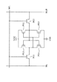
図1は、具体例に係るSRAMセルの回路図である。SRAMセルは、パスゲートトランジスタPG1とPG2、プルアップ(pull-up)トランジスタPU1とPU2、及び、プルダウントランジスタPD1とPD2を含んでいる。パスゲートトランジスタPG1 とPG2のゲートはワードライン WLにより制御され、ワードラインによって、現在の SRAMセルが選択されるかどうかを決定する。プルアップトランジスタPU1とPU2、プルダウントランジスタPD1とPD2により形成されるラッチは、ビットを保存する。保存されたビットは、ビットラインBLとBLB により、SRAMセルに書き込まれるか、SRAMセルから読み取られる。SRAMセルには、正の電源ノード VCCと電源ノード VSSにより電源が供給される。電源ノードVSSは電気的に接地されてもよい。 FIG. 1 is a circuit diagram of an SRAM cell according to a specific example. The SRAM cell includes pass gate transistors PG1 and PG2, pull-up transistors PU1 and PU2, and pull-down transistors PD1 and PD2. The gates of pass gate transistors PG1 and PG2 are controlled by word line WL, which determines whether the current SRAM cell is selected. A latch formed by pull-up transistors PU1 and PU2 and pull-down transistors PD1 and PD2 stores bits. The stored bits are written to or read from the SRAM cell by bit lines BL and BLB. The SRAM cell is powered by a positive power supply node VCC and a power supply node VSS. The power supply node VSS may be electrically grounded.
プルダウントランジスタPD1とPD2は、それぞれ、二以上の半導体フィンを含むマルチフィン型FinFETである。一方、パスゲートトランジスタPG1と PG2、及び、プルアップトランジスタPU1とPU2は、単一フィンFinFET、或いは、マルチフィン FinFETである。従って、プルダウントランジスタPD1とPD2、及び、パスゲートトランジスタPG1とPG2中のフィンの数を調整することにより、ベータ比率I_PD1/I_PG1、或いは、I_PD2/I_PG2 (ここで、I_PD1、 I_PD2、 I_PG1、及び、 I_PG2 は、それぞれ、トランジスタPD1、 PD2、 PG1、 及び、 PG2の駆動電流である)を、望ましい値、例えば、1以上に調整することができる。I_PU1/I_PG1 、或いは、I_PU2/I_PG2 (ここで、I_PU1 と I_PU2は、それぞれ、トランジスタPU1 と PU2の駆動電流である)で示されるアルファ比率も、望ましい値に調整できる。 Each of the pull-down transistors PD1 and PD2 is a multi-fin FinFET including two or more semiconductor fins. On the other hand, the pass gate transistors PG1 and PG2 and the pull-up transistors PU1 and PU2 are single-fin FinFETs or multi-fin FinFETs . Therefore, the beta ratio I_PD1 / I_PG1 or I_PD2 / I_PG2 (where I_PD1, I_PD2, I_PG1, and I_PG2 is a driving current of the transistors PD1, PD2, PG1, and PG2, respectively), and can be adjusted to a desired value, for example, 1 or more. The alpha ratio indicated by I_PU1 / I_PG1 or I_PU2 / I_PG2 (where I_PU1 and I_PU2 are the drive currents of the transistors PU1 and PU2, respectively) can also be adjusted to a desired value.
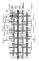
図2は、図1で示される具体例に係るSRAMセルの配置を示す図で、SRAM中のトランジスタに参照符号が付けられている。ユニットセルの境界(cell boundary)も示されている。図示された部分は、四個の同一構造のSRAMセルを含んでおり、これにより、2x2 アレイを形成している。具体例中、フィン、例えば、SRAMセル中のFin1とFin2は同じ幅を有するが、異なる幅を有していても良い。以下の説明中、トランジスタPG1、PD1、及び、PU1だけを含むSRAMセルの第一ポートだけが詳述され、トランジスタPG2、PD2、及び、PU2を含む第二ポートは、第一ポート中のトランジスタと本質的に同じ特徴を有する。よって、第二ポートの詳細は省略する。図2と図4〜図7には、様々な要素、例えば、VCC- contact、VSS- contact、butted- contact、BL- contactとBLB- contact も示され、各種コンタクトの作用も、それらの名前により表されている。説明を通じて、コンタクトは、コンタクトプラグとも称される。 FIG. 2 is a diagram showing the arrangement of the SRAM cell according to the specific example shown in FIG. 1, and reference numerals are assigned to the transistors in the SRAM. The cell boundary is also shown. The illustrated portion includes four identically structured SRAM cells, thereby forming a 2 × 2 array. In the specific example, fins, for example, Fin1 and Fin2 in the SRAM cell have the same width, but may have different widths. In the following description, only the first port of the SRAM cell that includes only the transistors PG1, PD1, and PU1, is detailed, and the second port that includes the transistors PG2, PD2, and PU2 Has essentially the same characteristics. Therefore, details of the second port are omitted. 2 and 4-7 also show various elements such as VCC-contact, VSS-contact, butted-contact, BL-contact and BLB-contact, and the action of the various contacts also depends on their names. It is represented. Throughout the description, the contact is also referred to as a contact plug.
プルダウントランジスタPD1 (PD-11とPD-12で示される2個のトランジスタを含んでいる)は、二個のフィンFin1 と Fin2を有し、Fin1 と Fin2は、互いに、物理的に分離されている。従って、プルダウントランジスタPD1は、二個のサブトランジスタPD-11と PD-12からなるダブルフィントランジスタで、サブトランジスタPD-11は、フィンFin1とゲートストリップ (ポリシリコンストリップ、或いは、金属合金ストリップ) G1により形成され、サブトランジスタPD-12 は、フィンFin2 とゲートストリップG1により形成されている。 The pull-down transistor PD1 (which includes two transistors designated PD-11 and PD-12) has two fins Fin1 and Fin2, which are physically separated from each other. . Therefore, the pull-down transistor PD1 is a double fin transistor composed of two subtransistors PD-11 and PD-12. The subtransistor PD-11 is composed of a fin Fin1 and a gate strip (polysilicon strip or metal alloy strip) G1. The sub-transistor PD-12 is formed by the fin Fin2 and the gate strip G1.
パスゲートトランジスタPG1は1フィンFin1だけを有する。従って、パスゲートトランジスタPG1は、フィンFin1とゲートストリップG2により形成される単一フィントランジスタである。図示された例では、ゲートストリップG2もフィン Fin2上に延伸されている。しかし、フィンFin2とゲートストリップ G2により形成されるトランジスタ (以下で、ダミートランジスタ Dummy1 と称される)のソース/ドレイン領域Dummy1-SD は、ビットラインコンタクトBL-contactから電気的に切り離され、これにより、トランジスタDummy1は、ダミートランジスタで、パスゲートトランジスタPG1を同時にオン、或いは、オフにしたりすることができない。従って、具体例中、全フィンは同じフィン幅を有し、ベータ比率は約2である。同様に、SRAMセルの第二ポートはダミートランジスタDummy2を含んでいる。 The pass gate transistor PG1 has only one fin Fin1. Accordingly, the pass gate transistor PG1 is a single fin transistor formed by the fin Fin1 and the gate strip G2. In the illustrated example, the gate strip G2 is also extended on the fin Fin2. However, the source / drain region Dummy1-SD of the transistor (hereinafter referred to as the dummy transistor Dummy1) formed by the fin Fin2 and the gate strip G2 is electrically disconnected from the bit line contact BL-contact. The transistor Dummy1 is a dummy transistor and cannot turn on or off the pass gate transistor PG1 at the same time. Thus, in the specific example, all fins have the same fin width and the beta ratio is about 2. Similarly, the second port of the SRAM cell includes a dummy transistor Dummy2.
具体例中、フィン Fin1はストレートフィンで、フィン Fin2 は、三つの部分Fin2-1、Fin2-2、及び、Fin2-3を有する屈曲フィンである。部分Fin2-1は、ソース、ドレイン、及び、サブトランジスタPD-12のチャネル領域を形成する。部分Fin2-3は、ゲートストリップ G2と、ダミートランジスタDummy1を形成する。部分Fin2-1とFin2-3はフィン Fin1に平行で、部分Fin2-2は平行ではなく、ストレートフィン Fin1に垂直である。 In the specific example, the fin Fin1 is a straight fin, and the fin Fin2 is a bent fin having three portions Fin2-1, Fin2-2, and Fin2-3. The portion Fin2-1 forms the source, drain, and channel region of the sub-transistor PD-12. The portion Fin2-3 forms a gate strip G2 and a dummy transistor Dummy1. The portions Fin2-1 and Fin2-3 are parallel to the fin Fin1, and the portion Fin2-2 is not parallel and is perpendicular to the straight fin Fin1.
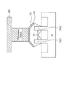
図3Aと図3Bは、図2で示される構造の断面図で、図2の線3-3に沿って断面された断面図であり、サブトランジスタPD-1とPD-12のソースとドレイン領域と交叉している。図3Aで示されるように、フィンFin1とFin2は近接して設置される。一具体例において、フィン Fin1とFin2 の距離 S1は、形成技術で許容される最小距離である。例えば、45 nm 技術では、距離 S1は約60〜約90nmである。別の具体例では、S1は約 60 nmより小さい。しかし、当業者なら、図示された寸法範囲は単なる例に過ぎず、使用する異なる形成技術により変化することが理解できる。フィン Fin1とFin2は、下方基板20と同じ材料、例えば、シリコン、シリコンゲルマニウム、シリコン炭素、或いは、類似物から形成される。エピタキシャル層22が、フィン Fin1 と Fin2 上に形成されて、物理的に分離されたフィンFin1と Fin2が電気的に相互接続されている。フィンFin1上に形成されるエピタキシャル層 22の部分は、フィン Fin2 上のエピタキシャル層 22 の部分と相互に一体化され、連続した半導体層 22を形成している。エピタキシャル層 22は、フィン Fin1とFin2とは異なる組成物によって形成されても良い。ソース/ドレインシリサイド領域 24 は、エピタキシャル層 22上に形成される。コンタクト VSS- contact、或いは、コンタクト PD-D (図2を参照)であるコンタクトが、ソース/ドレインシリサイド領域24上に形成され、これにより、フィンFin1 と Fin2に電気的に接続される。具体例中、コンタクトVSS-contactと PD-Dは、フィン Fin1 と Fin2間に水平に配置されているが、フィン Fin1 と Fin2の任意の一つ、或いは、両方の上に直接形成されてもよい。この具体例では、上面図からも分かるように、コンタクトVSS- contactと PD-D は方形である(図2)。
3A and 3B are cross-sectional views of the structure shown in FIG. 2, which is a cross-sectional view taken along line 3-3 in FIG. 2, and the source and drain regions of subtransistors PD-1 and PD-12. Crossed with. As shown in FIG. 3A, the fins Fin1 and Fin2 are installed close to each other. In one embodiment, the distance S1 between the fins Fin1 and Fin2 is the minimum distance allowed by the forming technology. For example, for 45 nm technology, the distance S1 is about 60 to about 90 nm. In another embodiment, S1 is less than about 60 nm. However, those skilled in the art will appreciate that the illustrated dimension ranges are merely examples and will vary with the different forming techniques used. The fins Fin1 and Fin2 are formed from the same material as the
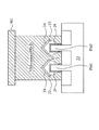
図3Bは別の具体例を示し、フィンFin1とFin2上に、エピタキシャル層 22 (点線で示される)がない、或いは、エピタキシャル層 22が形成されるが、フィンFin1とFin2上のエピタキシャル層 22の部分が一体化されていない。コンタクトVSS contact はサブトランジスタPD-11 と PD-12のソース上まで直接延伸し、接続されている。コンタクト PD-D は、サブトランジスタPD-11とPD-12のドレインまで直接延伸し、接続されている。本具体例において、コンタクトVSS-contactと PD-D は、異なる長さと幅の長方形である (上面図で見た場合) 。
FIG. 3B shows another specific example, where there is no epitaxial layer 22 (shown by a dotted line) on the fins Fin1 and Fin2, or the
図2をもう一度参照すると、サブプルダウントランジスタPD-11とPD-12のソースとドレイン部分のフィンFin1とFin2 は、互いに物理的に切り離されている。特に、45 nm、或いは、それ以下の技術が用いられる際、フィンFin1とFin2を接合することが工程上難しくなる場合、この工程を扱いやすいものにしている。 Referring to FIG. 2 again, the fins Fin1 and Fin2 of the source and drain portions of the sub pull-down transistors PD-11 and PD-12 are physically separated from each other. In particular, when a technique of 45 nm or less is used, if it is difficult to join the fins Fin1 and Fin2 in the process, this process is made easy to handle.
フィン Fin1とFin2間の距離S1が小さい場合、この問題は更に厳しくなる。しかし、図3A、或いは、図3B中のスキームを用いることにより、フィン Fin1と Fin2は、プロセスの困難度を増加させることなく、電気的に相互接続される。更に、フィンFin1とFin2間の距離 S1を、形成技術により許容される最小距離まで減少させることができる。従って、各SRAMセルは小チップ面積だけを占有する。 This problem becomes more severe when the distance S1 between the fins Fin1 and Fin2 is small. However, by using the scheme in FIG. 3A or FIG. 3B, the fins Fin1 and Fin2 are electrically interconnected without increasing the difficulty of the process. Furthermore, the distance S1 between the fins Fin1 and Fin2 can be reduced to the minimum distance allowed by the forming technique. Thus, each SRAM cell occupies only a small chip area.
フィン部分Fin2-3は、距離 S1より大きい距離 S2だけ、フィン Fin1から離される。具体例においては、距離S2は、距離S1より、約 125 パーセント、約 150 パーセント、或いは、約180パーセント大きい。従って、パスゲートトランジスタ PG1のソース/ドレイン領域に接続されるコンタクトBL- contactは、パスゲートトランジスタ PG1とダミートランジスタ Dummy1の各ソース/ドレイン領域とを電気的に不所望に接続しない。 The fin portion Fin2-3 is separated from the fin Fin1 by a distance S2 that is greater than the distance S1. In a specific example, the distance S2 is about 125 percent, about 150 percent, or about 180 percent greater than the distance S1 . Therefore, the contact BL-contact connected to the source / drain region of the pass gate transistor PG1 does not electrically undesirably connect the pass gate transistor PG1 and the source / drain regions of the dummy transistor Dummy1.
図4は、図1で示されるSRAMの別の配置図である。特別の定めがない限り、図4〜図7の同一の参考符号は、図2〜図3B中に示された同一の素子を示しているため、ここで詳述しない。図4の具体例は、フィン部分 Fin2-3が、近接するSRAMセルのフィン部分 Fin2-3 から切り離されていること以外は、図3で示される具体例と本質的に同じである。比較すると、図2に示されたSRAMセルのフィン部分 Fin2-3は、境界まで連続して延在し、近接するSRAMセルのフィン部分 Fin2-3と単一連続フィンを形成している。図4は、別のリソグラフマスクのパターンである切断ゲートCut-gateのパターンも説明している。フィンの形成は、フィンを形成するステップと、不要部分を除去するステップと、を含み、パターンCut-gate は、フィンの不要部分を除去するのに用いられる。距離S2は距離 S1より大きくから、フィンFin2 が容易に除去され、フィン Fin1 が誤って切断されることがないことが判る。フィンFin2を切断することにより、フィン部分 Fin2-3の後端キャップ Fin-End は、全セル境界から離れた位置にある。 FIG. 4 is another layout diagram of the SRAM shown in FIG. Unless otherwise specified, the same reference numerals in FIGS. 4-7 refer to the same elements shown in FIGS. 2-3B and will not be described in detail here. The specific example of FIG. 4 is essentially the same as the specific example shown in FIG. 3 except that the fin portion Fin2-3 is separated from the fin portion Fin2-3 of the adjacent SRAM cell. In comparison, the fin portion Fin2-3 of the SRAM cell shown in FIG. 2 extends continuously to the boundary, and forms a single continuous fin with the fin portion Fin2-3 of the adjacent SRAM cell. FIG. 4 also illustrates a cutting gate cut-gate pattern, which is another lithographic mask pattern. The formation of the fin includes a step of forming the fin and a step of removing the unnecessary portion, and the pattern Cut-gate is used to remove the unnecessary portion of the fin. Since the distance S2 is larger than the distance S1, it can be seen that the fin Fin2 is easily removed and the fin Fin1 is not cut by mistake. By cutting the fin Fin2, the rear end cap Fin-End of the fin portion Fin2-3 is located away from the whole cell boundary.
図5は、図1で示されるSRAMセルの別の配置を示す図である。この具体例では、ストレートフィン Fin1に平行であるストレートフィンFin3 が加えられている。フィンFin1とFin3間の距離S3は、距離 S1以上である。よって、プルダウントランジスタ PD は、サブトランジスタPD-11、PD-12、及び、PD-13からなるトリプルフィントランジスタである。コンタクトVSS Contactと PD-D は、本質的に、図3Aと図3Bで示されるのと同じスキームを用いて、サブプルダウントランジスタPD-11、PD-12、及び、PD-13のソースとドレイン領域に接続され、エピタキシャル層を通して、或いは、3個のフィンFin1、Fin2、Fin3上に直接延伸してそれらを電気的に接続する大きなコンタクトを通して、設けられている。 FIG. 5 is a diagram showing another arrangement of the SRAM cell shown in FIG. In this specific example, a straight fin Fin3 that is parallel to the straight fin Fin1 is added. The distance S3 between the fins Fin1 and Fin3 is not less than the distance S1. Therefore, the pull-down transistor PD is a triple fin transistor composed of sub-transistors PD-11, PD-12, and PD-13. Contacts VSS Contact and PD-D are essentially the same scheme as shown in FIGS. 3A and 3B, using the source and drain regions of sub-pulldown transistors PD-11, PD-12, and PD-13. And is provided through an epitaxial layer or through a large contact that extends directly over the three fins Fin1, Fin2 and Fin3 to electrically connect them.
パスゲートトランジスタ PG1 (PG-11 と PG-12で示される)は、サブトランジスタPG-11と PG-12からなるダブルフィントランジスタである。コンタクトVSS Contact と PD-D は、本質的に、図3A、或いは、図3Bで示されるのと同じスキームを用いて、サブプルダウントランジスタPD-11、PD-12、及び、PD-13のソースとドレイン領域に接続される。SRAMセルは、約 1.5に等しいベータ比率を有する。更に、プルアップトランジスタ PU1 は、サブトランジスタPU-11 と PU-12からなるダブルフィントランジスタで、フィン Fin4 と Fin5 、及び、ゲートストリップG1からなる。コンタクトVCC Contactは、本質的に、図3A、或いは、図3Bで示されるのと同じスキームを用いて、プルアップトランジスタのソース領域に接続される。従って、SRAMセルは、約1に等しいアルファ比率を有する。 The pass gate transistor PG1 (indicated by PG-11 and PG-12) is a double fin transistor composed of sub-transistors PG-11 and PG-12. Contacts VSS Contact and PD-D use essentially the same scheme as shown in FIG. 3A or FIG. 3B to connect the sources of sub-pull-down transistors PD-11, PD-12, and PD-13. Connected to the drain region. The SRAM cell has a beta ratio equal to about 1.5. Further, the pull-up transistor PU1 is a double fin transistor composed of sub-transistors PU-11 and PU-12, and is composed of fins Fin4 and Fin5, and a gate strip G1. Contact VCC Contact is essentially connected to the source region of the pull-up transistor using the same scheme shown in FIG. 3A or FIG. 3B. Thus, the SRAM cell has an alpha ratio equal to about 1.
図6は、図1で示されるSRAMの別の配置図である。本具体例は、フィン部分Fin2-3が、近接するSRAMセルのフィン部分Fin2-3’から切断されていること以外は、図5で示される具体例と本質的に同じである。同様に、切断ゲートCut-gate がフィン Fin2の切断に用いられる。よって、フィン Fin2の後端キャップは全セル境界から分離される。同様に、距離 S2は距離 S1より大きく、フィン Fin2 が容易に切断されて、フィン Fin1 が誤って切断されることがない。 FIG. 6 is another layout diagram of the SRAM shown in FIG. This specific example is essentially the same as the specific example shown in FIG. 5 except that the fin portion Fin2-3 is cut from the fin portion Fin2-3 'of the adjacent SRAM cell. Similarly, a cutting gate Cut-gate is used to cut the fin Fin2. Therefore, the rear end cap of the fin Fin2 is separated from the whole cell boundary. Similarly, the distance S2 is larger than the distance S1, and the fin Fin2 is easily cut and the fin Fin1 is not cut by mistake.
図7は、別の具体例による図1で示されるSRAMの更に別の配置図である。この具体例において、フィンFin1、Fin2、及び、Fin3 は平行で、全て、まっすぐである。フィン Fin1とFin3は距離S1を有し、 形成技術により許容される最小距離である。フィンFin1とFin 2は、距離S1より大きい距離 S2 を有する。距離S1 と S2の例の値(図3を参照)は、前の段落で既に説明されているので、説明を省略する。 FIG. 7 is another layout diagram of the SRAM shown in FIG. 1 according to another specific example. In this embodiment, fins Fin1, Fin2 and Fin3 are parallel and all straight. Fins Fin1 and Fin3 have a distance S1, which is the minimum distance allowed by the forming technology. The fins Fin1 and Fin2 have a distance S2 that is greater than the distance S1. The example values for the distances S1 and S2 (see FIG. 3) have already been explained in the previous paragraph and will not be explained.
図7において、フィンFin1とFin3間は距離が短いため、サブトランジスタPD-11 と PD-13のソース領域 (及び、ドレイン領域)は、本質的に、図3A、或いは、図3Bで示されるのと同じスキームを用いて(例えば、コンタクト VSS contact 1により)、相互接続される。一方、距離 S2は十分に大きく、サブトランジスタPD-11 と PD-12のソース領域 (及び、ドレイン領域)は、図3A、或いは、図3Bで示されるようなスキームにより接続されない。代わりに、コンタクトVSS contact 2 (サブトランジスタ PD-12のソースに接続される)は、金属線M1-connectにより、サブプルダウントランジスタPD-11と PD-13のソースに電気的に接続される。金属線M1- connectは、金属化層の底部 (通常はM1で、図3Aと図3Bを参照)にあり、コンタクト VSS contact1 とVSS contact2上方に、直接位置する。サブプルダウントランジスタPD-11、PD-12、及び、PD-13のドレイン側接続は、 基本的に、ソース側と同じである。 In FIG. 7, since the distance between the fins Fin1 and Fin3 is short, the source regions (and drain regions) of the subtransistors PD-11 and PD-13 are essentially shown in FIG. 3A or FIG. 3B. Are interconnected using the same scheme (eg by contact VSS contact 1). On the other hand, the distance S2 is sufficiently large, and the source regions (and drain regions) of the sub-transistors PD-11 and PD-12 are not connected by the scheme shown in FIG. 3A or FIG. 3B. Instead, contact VSS contact 2 (connected to the source of sub-transistor PD-12) is electrically connected to the sources of sub-pull-down transistors PD-11 and PD-13 by metal line M1-connect. The metal line M1-connect is at the bottom of the metallization layer (usually M1, see FIGS. 3A and 3B) and is located directly above the contacts VSS contact1 and VSS contact2. The drain side connection of the sub pull-down transistors PD-11, PD-12, and PD-13 is basically the same as the source side.
パスゲートトランジスタ PG1 (PG-11と PG-12を含み、PG-11と PG-12で示される)は、Fin3とゲートストリップG2からなるサブトランジスタPG-11と、フィン Fin1 とゲートストリップ G2からなるサブトランジスタ PG-12と、からなるダブルフィントランジスタである。ゲートストリップG2もフィン Fin2上に延伸することが観察される。トランジスタDummy1のソース/ドレイン領域Dummy1-SD は、ビットラインコンタクトBL contactから電気的に切り離されており、これにより、トランジスタDummy1もダミートランジスタで、サブパスゲートトランジスタPG-11 と PG-12と同時に、オン、オフにすることができない。従って、図7で示されるように、SRAMセルのベータ比率は約 1.5である。同様に、アルファ比率は約 1である。 Passgate transistor PG1 (including PG-11 and PG-12, indicated by PG-11 and PG-12) consists of sub-transistor PG-11 consisting of Fin3 and gate strip G2, and fin Fin1 and gate strip G2. This is a double fin transistor comprising a sub-transistor PG-12. It is observed that the gate strip G2 also extends over the fin Fin2. The source / drain region Dummy1-SD of the transistor Dummy1 is electrically disconnected from the bit line contact BL contact, so that the transistor Dummy1 is also a dummy transistor and is turned on simultaneously with the sub-pass gate transistors PG-11 and PG-12. Can't turn off. Therefore, as shown in FIG. 7, the beta ratio of the SRAM cell is about 1.5. Similarly, the alpha ratio is about 1.
具体例において、マルチフィンプルダウントランジスタは電気的に接続され、物理的に切り離されている。これは、フィンを屈曲すること、或いは、ダミートランジスタを形成することにより達成される。各配置は、特に、例えば、 45 nm 、或いは、それより小さい小型集積回路にとって、工程的に使用し易い。各SRAMセルのベータ比率は 1以上に増加し、セル安定性が改善される。 In a specific example, the multi-fin pull-down transistors are electrically connected and physically disconnected. This is achieved by bending the fins or forming dummy transistors. Each arrangement is easy to use in process, especially for small integrated circuits, eg 45 nm or smaller. The beta ratio of each SRAM cell increases to 1 or more, improving cell stability.
本発明では好ましい実施例を前述の通り開示したが、これらは決して本発明に限定するものではなく、当該技術を熟知する者なら誰でも、本発明の精神と領域を脱しない範囲内で各種の変形や修飾を加えることができ、従って本発明の保護範囲は、特許請求の範囲で指定した内容を基準とする。 In the present invention, preferred embodiments have been disclosed as described above. However, the present invention is not limited to the present invention, and any person who is familiar with the technology can use various methods within the spirit and scope of the present invention. Variations and modifications can be made, so the protection scope of the present invention is based on what is specified in the claims.
本発明に係る集積回路は、例えば、キャッシュメモリ等の高速メモリとして利用できる。 The integrated circuit according to the present invention can be used as a high-speed memory such as a cache memory, for example.
BL、BLB ビットライン
BL-contact、BLB-contact コンタクト
Cut-gate 切断ゲート
Dummy1、Dummy2 ダミートランジスタ
Dummy1-SD ダミートランジスタのソース/ドレイン領域
Fin1、Fin2、Fin2-1〜Fin2-3、Fin2-3’、Fin3、Fin4、Fin5 フィン
Fin-End 後端キャップ
G1、G2 ゲートストリップ
M1-connect 金属線
PD1、PD2 プルダウントランジスタ
PD-11、PD-12、PD-13、PD-21、PD-22 サブプルダウントランジスタ
PG1、PG2 パスゲートトランジスタ
PG-11、PG-12、PG-21、PG-22 サブパスゲートトランジスタ
PU1、PU2 プルアップトランジスタ
PU-11、PU-12、PU-21、PU-22 サブトランジスタ
VCC 正の電源ノード
VCC-contact、VSS-contact、Butted-contact、PD-D、VSS-contact1、VSS-contact2 コンタクト
VSS 電源ノード
S1、S2、S3 距離
WL ワードライン
BL, BLB bit line
BL-contact, BLB-contact contact
Cut-gate
Dummy1, Dummy2 dummy transistor
Dummy1-SD Dummy transistor source / drain region
Fin1, Fin2, Fin2-1 to Fin2-3, Fin2-3 ', Fin3, Fin4, Fin5 Fin
Fin-End rear end cap
G1, G2 gate strip
M1-connect metal wire
PD1, PD2 pull-down transistor
PD-11, PD-12, PD-13, PD-21, PD-22 Sub pull-down transistor
PG1, PG2 Pass gate transistor
PG-11, PG-12, PG-21, PG-22 Subpass gate transistor
PU1, PU2 pull-up transistor
PU-11, PU-12, PU-21, PU-22 Subtransistor
VCC Positive power node
VCC-contact, VSS-contact, Butted-contact, PD-D, VSS-contact1, VSS-contact2 Contact
VSS power node
S1, S2, S3 distance
WL word line
Claims (10)
第一ストレート(straight)フィンと、
前記第一ストレートフィンから物理的に切り離され、前記第一ストレートフィンに平行な第一部分と第二部分を有する屈曲(bended)フィンと、
前記第一ストレートフィンに平行でなく、前記第一部分と前記第二部分に相互接続される前記屈曲フィンの第三部分と、
第一ゲートストリップの部分を含み、前記第一ゲートストリップが、前記第一ストレートフィンと前記屈曲フィンの前記第一部分を有する第一、及び、第二サブプルダウントランジスタを形成するプルダウントランジスタと、
第二ゲートストリップの部分を含み、前記第二ゲートストリップが、前記第一ストレートフィンを有する第一サブパスゲートトランジスタを形成するパスゲートトランジスタと、
を含み、
前記屈曲フィンの前記第一部分と前記第一ストレートフィンは第一距離を有し、前記屈曲フィンの前記第二部分と前記第一ストレートフィンは、前記第一距離より大きい第二距離を有し、
前記プルダウントランジスタのフィンの第一の数は、前記パスゲートトランジスタのフィンの第二の数より多いことを特徴とする集積回路。 An integrated circuit structure comprising SRAM cells, wherein the SRAM cells are
The first straight fin,
A bent fin physically separated from the first straight fin and having a first portion and a second portion parallel to the first straight fin;
A third portion of the bent fin interconnected to the first portion and the second portion, not parallel to the first straight fin;
A first pull-down transistor comprising a first gate strip, wherein the first gate strip forms a first and second sub-pull-down transistor having the first straight fin and the first portion of the bent fin;
A pass gate transistor comprising a portion of a second gate strip, wherein the second gate strip forms a first sub-pass gate transistor having the first straight fin;
Including
The first portion of the bent fin and the first straight fin have a first distance, the second portion of the bent fin and the first straight fin have a second distance greater than the first distance,
The integrated circuit of claim 1, wherein the first number of fins of the pull-down transistor is greater than the second number of fins of the pass gate transistor.
前記第一ストレートフィンの一部上の第一エピタキシャル半導体領域と、
前記屈曲フィンの前記第一部分上にあり、且つ、前記第一エピタキシャル半導体領域と、連続した半導体領域を形成する第二エピタキシャル半導体領域と、
前記第一ストレートフィンと前記屈曲フィン間に水平に位置し、前記第一、及び、前記第二エピタキシャル半導体領域に電気的に接続されるコンタクトプラグと、
からなることを特徴とする請求項1に記載の集積回路。 The first distance is approximately equal to a minimum distance allowed by the integrated circuit formation technology, and the integrated circuit further comprises:
A first epitaxial semiconductor region on a portion of the first straight fin;
A second epitaxial semiconductor region on the first portion of the bent fin and forming the first epitaxial semiconductor region and a continuous semiconductor region;
A contact plug positioned horizontally between the first straight fin and the bent fin and electrically connected to the first and second epitaxial semiconductor regions;
The integrated circuit according to claim 1, comprising:
第一ストレートフィンと、屈曲フィンとを有し、
前記屈曲フィンは、前記第一ストレートフィンに平行な第一部分と、前記第一ストレートフィンに平行な第二部分と、前記第一ストレートフィンに平行でなく、前記第一部分と前記第二部分と相互接続される前記屈曲フィンの第三部分を有すると共に、
第一ゲートストリップの部分を含み、前記第一ゲートストリップが、前記第一ストレートフィンと前記屈曲フィンの前記第一部分を有する第一、及び、第二サブプルダウントランジスタを形成するプルダウントランジスタと、
第二ゲートストリップの部分を含み、前記第二ゲートストリップが、前記第一ストレートフィンを有する第一サブパスゲートトランジスタを形成すると共に、前記屈曲フィンの前記第二部分を有するダミートランジスタを形成し、前記第一サブパスゲートトランジスタと前記ダミートランジスタによって構成されたパスゲートトランジスタと備え、
前記屈曲フィンの前記第一部分と前記第一ストレートフィンは第一距離を有し、前記屈曲フィンの前記第二部分と前記第一ストレートフィンは、前記第一距離より大きい第二距離を有することを特徴とする集積回路構造。 An integrated circuit structure comprising SRAM cells, wherein the SRAM cells are
Having a first straight fin and a bent fin;
The bent fin includes a first part parallel to the first straight fin, a second part parallel to the first straight fin, and not parallel to the first straight fin. Having a third portion of the bent fin to be connected;
A first pull-down transistor comprising a first gate strip, wherein the first gate strip forms a first and second sub-pull-down transistor having the first straight fin and the first portion of the bent fin;
Including a portion of a second gate strip, the second gate strip forming a first subpass gate transistor having the first straight fin and forming a dummy transistor having the second portion of the bent fin , A first sub- pass gate transistor and a pass gate transistor constituted by the dummy transistor ;
The first part of the bent fin and the first straight fin have a first distance, and the second part of the bent fin and the first straight fin have a second distance greater than the first distance. Characteristic integrated circuit structure.
前記プルダウントランジスタは、更に、前記第二ストレートフィンの第一部分と前記第一ゲートストリップの追加部分とを含む第三サブプルダウントランジスタを含み、
前記パスゲートトランジスタは、更に、前記第二ストレートフィンの第二部分と、前記第二ゲートストリップの追加部分を含む第二サブパスゲートトランジスタを含むことを特徴とする請求項6に記載の集積回路構造。 Furthermore, it has a second straight fin,
The pull-down transistor further includes a third sub-pull-down transistor including a first portion of the second straight fin and an additional portion of the first gate strip;
7. The integrated circuit structure of claim 6, wherein the pass gate transistor further comprises a second sub-pass gate transistor including a second portion of the second straight fin and an additional portion of the second gate strip. .
第一ストレートフィンと、
前記第一ストレートフィンから物理的に切り離され、前記第一ストレートフィンに平行な第二ストレートフィンと、
第一ゲートストリップの部分を含み、前記第一ゲートストリップが、前記第一ストレートフィンの第一部分及び前記第二ストレートフィンの第一部分をそれぞれ備えた第一、及び、第二サブプルダウントランジスタを形成するプルダウントランジスタと、
第二ゲートストリップの部分を含み、前記第二ゲートストリップが、前記第一ストレートフィンの第二部分を有するパスゲートトランジスタの第一サブパスゲートトランジスタを形成すると共に、前記第二ゲートストリップが、前記第二ストレートフィンの第二部分に直接延伸し、ダミートランジスタを形成するパスゲートトランジスタと、
からなることを特徴とする集積回路構造。 An integrated circuit structure comprising SRAM cells, wherein the SRAM cells are
The first straight fin,
A second straight fin physically separated from the first straight fin and parallel to the first straight fin;
Including a portion of a first gate strip, wherein the first gate strip forms a first and second sub-pulldown transistor comprising a first portion of the first straight fin and a first portion of the second straight fin, respectively. A pull-down transistor;
Includes a portion of the second gate strips, said second gate strip, to form a first sub-pass gate transistor of Rupa scan gate transistor having a second portion of the first straight fin, said second gate strips A pass gate transistor extending directly to the second portion of the second straight fin to form a dummy transistor;
An integrated circuit structure comprising:
Applications Claiming Priority (4)
| Application Number | Priority Date | Filing Date | Title |
|---|---|---|---|
| US26734109P | 2009-12-07 | 2009-12-07 | |
| US61/267,341 | 2009-12-07 | ||
| US12/890,132 | 2010-09-24 | ||
| US12/890,132 US8258572B2 (en) | 2009-12-07 | 2010-09-24 | SRAM structure with FinFETs having multiple fins |
Publications (2)
| Publication Number | Publication Date |
|---|---|
| JP2011119741A JP2011119741A (en) | 2011-06-16 |
| JP5281069B2 true JP5281069B2 (en) | 2013-09-04 |
Family
ID=44081196
Family Applications (1)
| Application Number | Title | Priority Date | Filing Date |
|---|---|---|---|
| JP2010271209A Active JP5281069B2 (en) | 2009-12-07 | 2010-12-06 | Integrated circuit |
Country Status (6)
| Country | Link |
|---|---|
| US (2) | US8258572B2 (en) |
| JP (1) | JP5281069B2 (en) |
| KR (1) | KR101212368B1 (en) |
| CN (1) | CN102122660B (en) |
| DE (2) | DE102010053571B4 (en) |
| TW (1) | TWI474471B (en) |
Families Citing this family (63)
| Publication number | Priority date | Publication date | Assignee | Title |
|---|---|---|---|---|
| US8399931B2 (en) | 2010-06-30 | 2013-03-19 | Taiwan Semiconductor Manufacturing Company, Ltd. | Layout for multiple-fin SRAM cell |
| US8675397B2 (en) | 2010-06-25 | 2014-03-18 | Taiwan Semiconductor Manufacturing Company, Ltd. | Cell structure for dual-port SRAM |
| JP2012064854A (en) * | 2010-09-17 | 2012-03-29 | Toshiba Corp | Semiconductor device |
| US8561003B2 (en) | 2011-07-29 | 2013-10-15 | Synopsys, Inc. | N-channel and P-channel finFET cell architecture with inter-block insulator |
| US8595661B2 (en) * | 2011-07-29 | 2013-11-26 | Synopsys, Inc. | N-channel and p-channel finFET cell architecture |
| US8693235B2 (en) * | 2011-12-06 | 2014-04-08 | Taiwan Semiconductor Manufacturing Company, Ltd. | Methods and apparatus for finFET SRAM arrays in integrated circuits |
| US8802535B2 (en) * | 2012-05-02 | 2014-08-12 | International Business Machines Corporation | Doped core trigate FET structure and method |
| US9583398B2 (en) | 2012-06-29 | 2017-02-28 | Taiwan Semiconductor Manufacturing Company, Ltd. | Integrated circuit having FinFETS with different fin profiles |
| US9012287B2 (en) | 2012-11-14 | 2015-04-21 | Taiwan Semiconductor Manufacturing Company, Ltd. | Cell layout for SRAM FinFET transistors |
| US8779528B2 (en) * | 2012-11-30 | 2014-07-15 | Taiwan Semiconductor Manufacturing Company, Ltd. | SRAM cell comprising FinFETs |
| US8889561B2 (en) * | 2012-12-10 | 2014-11-18 | Globalfoundries Inc. | Double sidewall image transfer process |
| US9397217B2 (en) * | 2012-12-28 | 2016-07-19 | Taiwan Semiconductor Manufacturing Company, Ltd. | Contact structure of non-planar semiconductor device |
| US9812556B2 (en) | 2012-12-28 | 2017-11-07 | Renesas Electronics Corporation | Semiconductor device and method of manufacturing the semiconductor device |
| KR102049774B1 (en) * | 2013-01-24 | 2019-11-28 | 삼성전자 주식회사 | Semiconductor device and fabricated method thereof |
| US8921191B2 (en) * | 2013-02-05 | 2014-12-30 | GlobalFoundries, Inc. | Integrated circuits including FINFET devices with lower contact resistance and reduced parasitic capacitance and methods for fabricating the same |
| US8796093B1 (en) * | 2013-03-14 | 2014-08-05 | International Business Machines Corporation | Doping of FinFET structures |
| JP6224818B2 (en) * | 2013-03-30 | 2017-11-01 | インテル・コーポレーション | Integrated circuit and method of forming an integrated circuit |
| KR102072410B1 (en) | 2013-08-07 | 2020-02-03 | 삼성전자 주식회사 | Semiconductor device and fabricated method thereof |
| CN105531813B (en) * | 2013-09-04 | 2018-10-12 | 株式会社索思未来 | Semiconductor device |
| US9048123B2 (en) * | 2013-09-19 | 2015-06-02 | International Business Machines Corporation | Interdigitated finFETs |
| US9444460B1 (en) * | 2013-11-22 | 2016-09-13 | Altera Corporation | Integrated circuits with programmable overdrive capabilities |
| US9312273B2 (en) | 2013-12-02 | 2016-04-12 | International Business Machines Corporation | Structure and method to reduce crystal defects in epitaxial fin merge using nitride deposition |
| US9257439B2 (en) * | 2014-02-27 | 2016-02-09 | Taiwan Semiconductor Manufacturing Company, Ltd. | Structure and method for FinFET SRAM |
| US9224842B2 (en) * | 2014-04-22 | 2015-12-29 | Globalfoundries Inc. | Patterning multiple, dense features in a semiconductor device using a memorization layer |
| WO2015180595A1 (en) * | 2014-05-27 | 2015-12-03 | Mediatek Inc. | Fin field-effect transistor gated diode |
| US9852252B2 (en) | 2014-08-22 | 2017-12-26 | Samsung Electronics Co., Ltd. | Standard cell library and methods of using the same |
| US10242148B2 (en) * | 2014-08-25 | 2019-03-26 | Mediatek Inc. | Integrated circuit and routing design of the same |
| US9299706B1 (en) * | 2014-09-25 | 2016-03-29 | International Business Machines Corporation | Single source/drain epitaxy for co-integrating nFET semiconductor fins and pFET semiconductor fins |
| KR102288869B1 (en) * | 2014-10-01 | 2021-08-10 | 삼성전자주식회사 | System on chip |
| US9418896B2 (en) | 2014-11-12 | 2016-08-16 | Samsung Electronics Co., Ltd. | Semiconductor device and fabricating method thereof |
| US9859286B2 (en) * | 2014-12-23 | 2018-01-02 | International Business Machines Corporation | Low-drive current FinFET structure for improving circuit density of ratioed logic in SRAM devices |
| KR102193633B1 (en) * | 2014-12-30 | 2020-12-21 | 삼성전자주식회사 | Dual-port sram devices and methods of manufacturing the same |
| US9991384B2 (en) * | 2015-01-15 | 2018-06-05 | Taiwan Semiconductor Manufacturing Co., Ltd. | Semiconductor device including fin structures and manufacturing method thereof |
| KR102352153B1 (en) | 2015-03-25 | 2022-01-17 | 삼성전자주식회사 | Integrated circuit device and method for manufacturing the same |
| KR102316119B1 (en) * | 2015-04-02 | 2021-10-21 | 삼성전자주식회사 | Semiconductor device |
| KR102170701B1 (en) * | 2015-04-15 | 2020-10-27 | 삼성전자주식회사 | Semiconductor device and method of fabricating the same |
| US9391080B1 (en) * | 2015-04-28 | 2016-07-12 | Globalfoundries Inc. | Memory bit cell for reduced layout area |
| KR102400375B1 (en) * | 2015-04-30 | 2022-05-20 | 삼성전자주식회사 | Semiconductor devices and methods of manufacturing the same |
| KR20160136715A (en) * | 2015-05-20 | 2016-11-30 | 삼성전자주식회사 | Semiconductor devices and methods of manufacturing the same |
| US9922978B2 (en) * | 2015-08-21 | 2018-03-20 | Taiwan Semiconductor Manufacturing Co., Ltd | Semiconductor structure with recessed source/drain structure and method for forming the same |
| US9496269B1 (en) * | 2015-10-29 | 2016-11-15 | Taiwan Semiconductor Manufacturing Co., Ltd. | Static random access memory |
| US10121534B1 (en) * | 2015-12-18 | 2018-11-06 | Altera Corporation | Integrated circuit with overdriven and underdriven pass gates |
| US9455314B1 (en) | 2016-02-05 | 2016-09-27 | International Business Machines Corporation | Y-FET with self-aligned punch-through-stop (PTS) doping |
| CN106057900B (en) * | 2016-06-17 | 2019-07-30 | 中国科学院微电子研究所 | Epitaxial layer-based semiconductor device, method of manufacturing the same, and electronic apparatus including the same |
| US10366196B2 (en) * | 2016-06-22 | 2019-07-30 | Qualcomm Incorporated | Standard cell architecture for diffusion based on fin count |
| US9892781B2 (en) | 2016-06-30 | 2018-02-13 | Taiwan Semiconductor Manufacturing Co., Ltd. | Cell structure for dual-port static random access memory |
| TWI675454B (en) * | 2016-07-04 | 2019-10-21 | 聯華電子股份有限公司 | Layout pattern for static random access memory |
| US9837405B1 (en) | 2016-08-02 | 2017-12-05 | International Business Machines Corporation | Fabrication of a vertical fin field effect transistor having a consistent channel width |
| US10515969B2 (en) | 2016-11-17 | 2019-12-24 | Taiwan Semiconductor Manufacturing Co., Ltd. | Semiconductor device and manufacturing method thereof |
| US10707328B2 (en) | 2016-11-30 | 2020-07-07 | Taiwan Semiconductor Manufacturing Co., Ltd. | Method of forming epitaxial fin structures of finFET |
| CN106601732B (en) * | 2016-12-21 | 2022-07-12 | 台湾积体电路制造股份有限公司 | Element grid layout structure and method for forming element grid |
| TWI699781B (en) * | 2016-12-28 | 2020-07-21 | 聯華電子股份有限公司 | Static random-access memory device |
| US11545495B2 (en) | 2017-06-29 | 2023-01-03 | Taiwan Semiconductor Manufacturing Co., Ltd. | Preventing gate-to-contact bridging by reducing contact dimensions in FinFET SRAM |
| KR102494918B1 (en) * | 2017-09-12 | 2023-02-02 | 삼성전자주식회사 | A semiconductor device |
| US10529712B2 (en) | 2017-11-07 | 2020-01-07 | Samsung Electronics Co., Ltd. | Semiconductor device |
| CN109979881B (en) * | 2017-12-28 | 2023-07-18 | 中芯国际集成电路制造(北京)有限公司 | The structure of static random access memory and its formation method |
| US10797223B2 (en) * | 2018-01-29 | 2020-10-06 | Globalfoundries Singapore Pte. Ltd. | Integrated circuits with magnetic random access memory (MRAM) devices and methods for fabricating such devices |
| US10515954B2 (en) * | 2018-03-18 | 2019-12-24 | Taiwan Semiconductor Manufacturing Co., Ltd. | Semiconductor device having fin structures of varying dimensions |
| US11056394B2 (en) | 2018-06-28 | 2021-07-06 | Taiwan Semiconductor Manufacturing Co., Ltd. | Methods for fabricating FinFETs having different fin numbers and corresponding FinFETs thereof |
| US11094695B2 (en) * | 2019-05-17 | 2021-08-17 | Taiwan Semiconductor Manufacturing Co., Ltd. | Integrated circuit device and method of forming the same |
| CN110534562A (en) * | 2019-08-29 | 2019-12-03 | 上海华力集成电路制造有限公司 | Static random access memory |
| CN113809083B (en) | 2020-06-11 | 2024-12-10 | 联华电子股份有限公司 | Static random access memory and manufacturing method thereof |
| CN113054006A (en) * | 2021-03-18 | 2021-06-29 | 广东省大湾区集成电路与系统应用研究院 | Semiconductor device layout structure |
Family Cites Families (33)
| Publication number | Priority date | Publication date | Assignee | Title |
|---|---|---|---|---|
| JP3526553B2 (en) * | 2001-01-26 | 2004-05-17 | 松下電器産業株式会社 | SRAM device |
| US7358121B2 (en) | 2002-08-23 | 2008-04-15 | Intel Corporation | Tri-gate devices and methods of fabrication |
| US6706571B1 (en) | 2002-10-22 | 2004-03-16 | Advanced Micro Devices, Inc. | Method for forming multiple structures in a semiconductor device |
| US6970373B2 (en) * | 2003-10-02 | 2005-11-29 | Intel Corporation | Method and apparatus for improving stability of a 6T CMOS SRAM cell |
| JP2005142289A (en) * | 2003-11-05 | 2005-06-02 | Toshiba Corp | Semiconductor memory device |
| KR100513405B1 (en) | 2003-12-16 | 2005-09-09 | 삼성전자주식회사 | Method for forming fin field effect transistor |
| KR100781538B1 (en) * | 2004-02-07 | 2007-12-03 | 삼성전자주식회사 | Method for manufacturing active structure for improved multi-gate transistor, active structure and multi-gate transistor manufactured thereby |
| JP4195409B2 (en) * | 2004-04-09 | 2008-12-10 | 株式会社東芝 | Semiconductor memory device |
| JP2005302231A (en) * | 2004-04-15 | 2005-10-27 | Toshiba Corp | Static random access memory |
| US7253493B2 (en) * | 2004-08-24 | 2007-08-07 | Micron Technology, Inc. | High density access transistor having increased channel width and methods of fabricating such devices |
| US7465973B2 (en) * | 2004-12-03 | 2008-12-16 | International Business Machines Corporation | Integrated circuit having gates and active regions forming a regular grating |
| US7265008B2 (en) | 2005-07-01 | 2007-09-04 | Synopsys, Inc. | Method of IC production using corrugated substrate |
| US7807523B2 (en) | 2005-07-01 | 2010-10-05 | Synopsys, Inc. | Sequential selective epitaxial growth |
| US8466490B2 (en) | 2005-07-01 | 2013-06-18 | Synopsys, Inc. | Enhanced segmented channel MOS transistor with multi layer regions |
| US7605449B2 (en) | 2005-07-01 | 2009-10-20 | Synopsys, Inc. | Enhanced segmented channel MOS transistor with high-permittivity dielectric isolation material |
| US7508031B2 (en) | 2005-07-01 | 2009-03-24 | Synopsys, Inc. | Enhanced segmented channel MOS transistor with narrowed base regions |
| US7190050B2 (en) | 2005-07-01 | 2007-03-13 | Synopsys, Inc. | Integrated circuit on corrugated substrate |
| US7247887B2 (en) | 2005-07-01 | 2007-07-24 | Synopsys, Inc. | Segmented channel MOS transistor |
| WO2007063990A1 (en) * | 2005-12-02 | 2007-06-07 | Nec Corporation | Semiconductor device and method for manufacturing same |
| JP2008034037A (en) * | 2006-07-28 | 2008-02-14 | Toshiba Corp | Semiconductor memory device |
| US7592675B2 (en) * | 2006-10-02 | 2009-09-22 | Taiwan Semiconductor Manufacutring Company, Ltd. | Partial FinFET memory cell |
| US7812373B2 (en) * | 2007-02-12 | 2010-10-12 | Infineon Technologies Ag | MuGFET array layout |
| US7738282B2 (en) * | 2007-02-15 | 2010-06-15 | Taiwan Semiconductor Manufacturing Company, Ltd. | Cell structure of dual port SRAM |
| US20080212392A1 (en) * | 2007-03-02 | 2008-09-04 | Infineon Technologies | Multiple port mugfet sram |
| JP4461154B2 (en) * | 2007-05-15 | 2010-05-12 | 株式会社東芝 | Semiconductor device |
| US7939862B2 (en) | 2007-05-30 | 2011-05-10 | Synopsys, Inc. | Stress-enhanced performance of a FinFet using surface/channel orientations and strained capping layers |
| JP4445521B2 (en) | 2007-06-15 | 2010-04-07 | 株式会社東芝 | Semiconductor device |
| JP2009130210A (en) * | 2007-11-26 | 2009-06-11 | Toshiba Corp | Semiconductor device |
| WO2009122579A1 (en) * | 2008-04-03 | 2009-10-08 | 日本ユニサンティスエレクトロニクス株式会社 | Method and device for improving stability of 6t sgt cmos sram cell |
| US20110018064A1 (en) * | 2008-04-04 | 2011-01-27 | Nxp B.V. | Sram cell comprising finfets |
| US7829951B2 (en) * | 2008-11-06 | 2010-11-09 | Qualcomm Incorporated | Method of fabricating a fin field effect transistor (FinFET) device |
| JP5322668B2 (en) * | 2009-01-21 | 2013-10-23 | 株式会社東芝 | Semiconductor device manufacturing method and photomask |
| US8018007B2 (en) * | 2009-07-20 | 2011-09-13 | International Business Machines Corporation | Selective floating body SRAM cell |
-
2010
- 2010-09-24 US US12/890,132 patent/US8258572B2/en active Active
- 2010-12-03 KR KR1020100122452A patent/KR101212368B1/en active Active
- 2010-12-06 DE DE102010053571.0A patent/DE102010053571B4/en active Active
- 2010-12-06 CN CN2010105813113A patent/CN102122660B/en active Active
- 2010-12-06 DE DE102010064570.2A patent/DE102010064570B3/en active Active
- 2010-12-06 JP JP2010271209A patent/JP5281069B2/en active Active
- 2010-12-07 TW TW99142544A patent/TWI474471B/en active
-
2012
- 2012-08-29 US US13/598,093 patent/US8809963B2/en active Active
Also Published As
| Publication number | Publication date |
|---|---|
| KR20110065355A (en) | 2011-06-15 |
| TW201123430A (en) | 2011-07-01 |
| JP2011119741A (en) | 2011-06-16 |
| TWI474471B (en) | 2015-02-21 |
| CN102122660B (en) | 2012-12-19 |
| DE102010064570B3 (en) | 2018-04-26 |
| US8809963B2 (en) | 2014-08-19 |
| US20110133285A1 (en) | 2011-06-09 |
| US20120319212A1 (en) | 2012-12-20 |
| CN102122660A (en) | 2011-07-13 |
| DE102010053571B4 (en) | 2014-07-10 |
| US8258572B2 (en) | 2012-09-04 |
| DE102010053571A1 (en) | 2011-06-09 |
| KR101212368B1 (en) | 2012-12-13 |
Similar Documents
| Publication | Publication Date | Title |
|---|---|---|
| JP5281069B2 (en) | Integrated circuit | |
| US12171092B2 (en) | Layout of static random access memory periphery circuit | |
| US20240292591A1 (en) | Memory devices with gate all around transistors | |
| JP4855786B2 (en) | Semiconductor device | |
| US10163488B2 (en) | SRAM structure with reduced capacitance and resistance | |
| JP5232201B2 (en) | Dual port SRAM cell structure | |
| CN103151070B (en) | For the method and apparatus of FinFET SRAM array integrated circuit | |
| US20110062523A1 (en) | Semiconductor memory device and production method thereof | |
| KR20140074873A (en) | Sram cells and arrays | |
| JP2005142289A (en) | Semiconductor memory device | |
| TW202205285A (en) | Semiconductor device | |
| KR100665853B1 (en) | Stacked memory cells suitable for use in highly integrated static random access memories | |
| US6445017B2 (en) | Full CMOS SRAM cell | |
| US10868019B2 (en) | Semiconductor device having strap cell | |
| TWI897287B (en) | Semiconductor structure, memory structure, and semiconductor device | |
| CN117082852A (en) | SRAM memory cell structure and method of forming the same |
Legal Events
| Date | Code | Title | Description |
|---|---|---|---|
| A131 | Notification of reasons for refusal |
Free format text: JAPANESE INTERMEDIATE CODE: A131 Effective date: 20130116 |
|
| A977 | Report on retrieval |
Free format text: JAPANESE INTERMEDIATE CODE: A971007 Effective date: 20130117 |
|
| A521 | Request for written amendment filed |
Free format text: JAPANESE INTERMEDIATE CODE: A523 Effective date: 20130411 |
|
| TRDD | Decision of grant or rejection written | ||
| A01 | Written decision to grant a patent or to grant a registration (utility model) |
Free format text: JAPANESE INTERMEDIATE CODE: A01 Effective date: 20130501 |
|
| A61 | First payment of annual fees (during grant procedure) |
Free format text: JAPANESE INTERMEDIATE CODE: A61 Effective date: 20130523 |
|
| R150 | Certificate of patent or registration of utility model |
Free format text: JAPANESE INTERMEDIATE CODE: R150 Ref document number: 5281069 Country of ref document: JP Free format text: JAPANESE INTERMEDIATE CODE: R150 |
|
| R250 | Receipt of annual fees |
Free format text: JAPANESE INTERMEDIATE CODE: R250 |
|
| R250 | Receipt of annual fees |
Free format text: JAPANESE INTERMEDIATE CODE: R250 |
|
| R250 | Receipt of annual fees |
Free format text: JAPANESE INTERMEDIATE CODE: R250 |
|
| R250 | Receipt of annual fees |
Free format text: JAPANESE INTERMEDIATE CODE: R250 |
|
| R250 | Receipt of annual fees |
Free format text: JAPANESE INTERMEDIATE CODE: R250 |
|
| R250 | Receipt of annual fees |
Free format text: JAPANESE INTERMEDIATE CODE: R250 |
|
| R250 | Receipt of annual fees |
Free format text: JAPANESE INTERMEDIATE CODE: R250 |
|
| R250 | Receipt of annual fees |
Free format text: JAPANESE INTERMEDIATE CODE: R250 |
|
| R250 | Receipt of annual fees |
Free format text: JAPANESE INTERMEDIATE CODE: R250 |
|
| R250 | Receipt of annual fees |
Free format text: JAPANESE INTERMEDIATE CODE: R250 |