JP5232394B2 - 半導体装置の製造方法 - Google Patents
半導体装置の製造方法 Download PDFInfo
- Publication number
- JP5232394B2 JP5232394B2 JP2007049654A JP2007049654A JP5232394B2 JP 5232394 B2 JP5232394 B2 JP 5232394B2 JP 2007049654 A JP2007049654 A JP 2007049654A JP 2007049654 A JP2007049654 A JP 2007049654A JP 5232394 B2 JP5232394 B2 JP 5232394B2
- Authority
- JP
- Japan
- Prior art keywords
- lead
- die pad
- support portion
- sealing resin
- semiconductor device
- Prior art date
- Legal status (The legal status is an assumption and is not a legal conclusion. Google has not performed a legal analysis and makes no representation as to the accuracy of the status listed.)
- Active
Links
Images


Classifications
-
- H—ELECTRICITY
- H01—ELECTRIC ELEMENTS
- H01L—SEMICONDUCTOR DEVICES NOT COVERED BY CLASS H10
- H01L24/00—Arrangements for connecting or disconnecting semiconductor or solid-state bodies; Methods or apparatus related thereto
- H01L24/93—Batch processes
- H01L24/95—Batch processes at chip-level, i.e. with connecting carried out on a plurality of singulated devices, i.e. on diced chips
- H01L24/97—Batch processes at chip-level, i.e. with connecting carried out on a plurality of singulated devices, i.e. on diced chips the devices being connected to a common substrate, e.g. interposer, said common substrate being separable into individual assemblies after connecting
-
- H—ELECTRICITY
- H01—ELECTRIC ELEMENTS
- H01L—SEMICONDUCTOR DEVICES NOT COVERED BY CLASS H10
- H01L2224/00—Indexing scheme for arrangements for connecting or disconnecting semiconductor or solid-state bodies and methods related thereto as covered by H01L24/00
- H01L2224/01—Means for bonding being attached to, or being formed on, the surface to be connected, e.g. chip-to-package, die-attach, "first-level" interconnects; Manufacturing methods related thereto
- H01L2224/42—Wire connectors; Manufacturing methods related thereto
- H01L2224/47—Structure, shape, material or disposition of the wire connectors after the connecting process
- H01L2224/48—Structure, shape, material or disposition of the wire connectors after the connecting process of an individual wire connector
- H01L2224/4805—Shape
- H01L2224/4809—Loop shape
- H01L2224/48091—Arched
-
- H—ELECTRICITY
- H01—ELECTRIC ELEMENTS
- H01L—SEMICONDUCTOR DEVICES NOT COVERED BY CLASS H10
- H01L2224/00—Indexing scheme for arrangements for connecting or disconnecting semiconductor or solid-state bodies and methods related thereto as covered by H01L24/00
- H01L2224/01—Means for bonding being attached to, or being formed on, the surface to be connected, e.g. chip-to-package, die-attach, "first-level" interconnects; Manufacturing methods related thereto
- H01L2224/42—Wire connectors; Manufacturing methods related thereto
- H01L2224/47—Structure, shape, material or disposition of the wire connectors after the connecting process
- H01L2224/48—Structure, shape, material or disposition of the wire connectors after the connecting process of an individual wire connector
- H01L2224/481—Disposition
- H01L2224/48151—Connecting between a semiconductor or solid-state body and an item not being a semiconductor or solid-state body, e.g. chip-to-substrate, chip-to-passive
- H01L2224/48221—Connecting between a semiconductor or solid-state body and an item not being a semiconductor or solid-state body, e.g. chip-to-substrate, chip-to-passive the body and the item being stacked
- H01L2224/48245—Connecting between a semiconductor or solid-state body and an item not being a semiconductor or solid-state body, e.g. chip-to-substrate, chip-to-passive the body and the item being stacked the item being metallic
- H01L2224/48247—Connecting between a semiconductor or solid-state body and an item not being a semiconductor or solid-state body, e.g. chip-to-substrate, chip-to-passive the body and the item being stacked the item being metallic connecting the wire to a bond pad of the item
Description
QFNが適用された半導体装置は、たとえば、MAP(Molded Array Packaging)方式により作製される。MAP方式では、リードフレーム上で複数の半導体チップが封止樹脂により一括して封止された後、1つの半導体チップを備える半導体装置の個体に切り分けられる。
イシングブレードを用いないことにより、各リードにおけるばりの発生を防止することが
できる。
また、請求項2記載の発明は、前記支持部除去工程は、前記リードの前記ダイパッドから遠い側の端部に前記第1面から前記ダイパッドへ向かって凹状に拡がって前記第2面に至る端面が形成されるまで、前記支持部だけでなく、前記リードもエッチングする工程を含む、請求項1に記載の半導体装置の製造方法である。
図1は、本発明の一実施形態に係る半導体装置の図解的な断面図である。
半導体装置1は、QFNが適用された半導体装置である。この半導体装置1は、半導体チップ2と、この半導体チップ2を支持するダイパッド3と、半導体チップ2と電気的に接続される複数のリード4と、これらを封止する封止樹脂5とを備えている。
ダイパッド3は、平面視矩形状の本体部7と、本体部7の周囲を取り囲む平面視矩形枠状の抜け止め部8とを一体的に備えている。
本体部7は、その下面7Aが封止樹脂5の下面5Aから露出している。この封止樹脂5の下面5Aから露出する本体部7の下面7Aには、たとえば、半田めっき層(図示せず)が形成されている。
各リード4は、ダイパッド3の側面と直交する方向(ダイパッド3との対向方向)に長尺な平面視矩形状に形成されている。そして、各リード4は、本体部9と、抜け止め部10とを一体的に備えている。
抜け止め部10は、下面側からのエッチング加工により、本体部9よりも薄く形成されている。抜け止め部10の上面は、本体部9の上面と面一をなしている。半導体チップ2とともにリード4を樹脂封止した状態では、抜け止め部10の下方に封止樹脂5が回り込むから、リード4の封止樹脂5からの抜け防止が図られる。
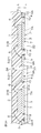
図2は、半導体装置1の製造に用いられるリードフレームの一部を示す底面図である。
半導体装置1は、後述するように、リードフレーム21を用いたMAP方式により製造される。
ダイパッド3は、各角部と支持部22との間に架設される吊りリード23によって支持されている。
図3A〜3Fは、半導体装置1の製造工程を順に示す図解的な断面図である。
すべての半導体チップ2のワイヤボンディングが完了すると、図3Bに示すように、リードフレーム21が成形金型にセットされ、リードフレーム21上のすべての半導体チップ2がリードフレーム21とともに封止樹脂31により一括して封止される。このとき、封止樹脂31は、その下面31Aからダイパッド3の本体部7の下面7A、リード4の本体部9の下面9Aおよびこれに連続する支持部22の下面22Aが露出するように形成される。そして、封止樹脂31から露出するリードフレーム21の下面に半田めっき層(図示せず)が形成される。
その後、図3Dに示すように、リードフレーム21の支持部22上に設定されたダイシングラインに沿って、ダイシングソー33が封止樹脂31の上面31B側から入れられ、支持部22上の封止樹脂31および支持部22の一部が除去される。ダイシングソー33は、支持部22を貫通せず、いわゆるハーフカットにより、支持部22の下面22A側の一部が残存する。
その後、図3Fに示すように、溝34にエッチング液が供給される。溝34が支持部に達しているので、溝34にエッチング液が供給されると、そのエッチング液によって支持部22がエッチングされる。このエッチングは、下方向だけでなく、これと直交する横方向にも進行する。そのため、支持部22だけでなく、リード4および吊りリード23の一部もエッチングされる。この結果、エッチングにより支持部22が除去された時点で、各リード4が個片化し、各リード4は、ダイパッド3側と反対側の端部に断面略1/4円形状の凹部11を有する。また、各吊りリード23の支持部22からの切り離しが達成される。その結果、半導体チップ2、ダイパッド3、リード4および封止樹脂5を備える半導体装置1の個体が得られる。
以上、本発明の一実施形態を説明したが、本発明は、他の形態で実施することが可能である。たとえば、QFNが適用された半導体装置を取り上げたが、本発明は、SON(Small Outlined Non-leaded Package)など、他の種類のノンリードパッケージが適用された半導体装置に適用することもできる。
2 半導体チップ
3 ダイパッド
4 リード
5 封止樹脂
6 ボンディングワイヤ
9 本体部
9A 下面(第2面)
9B 上面(第1面)
21 リードフレーム
22 支持部
22A 下面
31 封止樹脂
31B 上面
34 溝
Claims (2)
- ダイパッドと、前記ダイパッドの周囲に配置されて、前記ダイパッドとの対向方向に延びるリードと、前記リードの前記ダイパッドから遠い側の端部が接続された支持部とを一体的に備えるリードフレームを用いて、半導体装置を製造する方法であって、
前記ダイパッド上に半導体チップをダイボンディングし、前記半導体チップと前記リードとをボンディングワイヤで電気的に接続するボンディング工程と、
前記ボンディング工程後、前記リードにおける前記ボンディングワイヤが接続される第1面と反対側の第2面および前記支持部における前記第2面に連続する面が封止樹脂から露出するように、前記半導体チップを前記リードフレームとともに前記封止樹脂により封止する封止工程と、
前記支持部上の前記封止樹脂を除去し、前記封止樹脂における前記リードが露出する面と反対側の面から前記支持部に達する溝を形成する溝形成工程と、
前記溝にエッチング液を供給して、前記支持部をエッチングにより除去する支持部除去工程とを含む、半導体装置の製造方法。 - 前記支持部除去工程は、前記リードの前記ダイパッドから遠い側の端部に前記第1面から前記ダイパッドへ向かって凹状に拡がって前記第2面に至る端面が形成されるまで、前記支持部だけでなく、前記リードもエッチングする工程を含む、請求項1に記載の半導体装置の製造方法。
Priority Applications (1)
| Application Number | Priority Date | Filing Date | Title |
|---|---|---|---|
| JP2007049654A JP5232394B2 (ja) | 2007-02-28 | 2007-02-28 | 半導体装置の製造方法 |
Applications Claiming Priority (1)
| Application Number | Priority Date | Filing Date | Title |
|---|---|---|---|
| JP2007049654A JP5232394B2 (ja) | 2007-02-28 | 2007-02-28 | 半導体装置の製造方法 |
Publications (3)
| Publication Number | Publication Date |
|---|---|
| JP2008218469A JP2008218469A (ja) | 2008-09-18 |
| JP2008218469A5 JP2008218469A5 (ja) | 2010-03-18 |
| JP5232394B2 true JP5232394B2 (ja) | 2013-07-10 |
Family
ID=39838216
Family Applications (1)
| Application Number | Title | Priority Date | Filing Date |
|---|---|---|---|
| JP2007049654A Active JP5232394B2 (ja) | 2007-02-28 | 2007-02-28 | 半導体装置の製造方法 |
Country Status (1)
| Country | Link |
|---|---|
| JP (1) | JP5232394B2 (ja) |
Families Citing this family (11)
| Publication number | Priority date | Publication date | Assignee | Title |
|---|---|---|---|---|
| JP5010716B2 (ja) | 2010-01-29 | 2012-08-29 | 株式会社東芝 | Ledパッケージ |
| JP2011159767A (ja) | 2010-01-29 | 2011-08-18 | Toshiba Corp | Ledパッケージ及びその製造方法 |
| JP5383611B2 (ja) * | 2010-01-29 | 2014-01-08 | 株式会社東芝 | Ledパッケージ |
| JP4951090B2 (ja) | 2010-01-29 | 2012-06-13 | 株式会社東芝 | Ledパッケージ |
| JP5010693B2 (ja) | 2010-01-29 | 2012-08-29 | 株式会社東芝 | Ledパッケージ |
| MY155671A (en) * | 2010-01-29 | 2015-11-13 | Toshiba Kk | LED package and method for manufacturing same |
| JP2011165833A (ja) | 2010-02-08 | 2011-08-25 | Toshiba Corp | Ledモジュール |
| JP2011216615A (ja) * | 2010-03-31 | 2011-10-27 | Renesas Electronics Corp | 半導体装置の製造方法 |
| KR101450216B1 (ko) * | 2012-08-24 | 2014-10-14 | 주식회사 씨티랩 | 반도체 소자 구조물을 제조하는 방법 |
| JP7144157B2 (ja) | 2018-03-08 | 2022-09-29 | エイブリック株式会社 | 半導体装置およびその製造方法 |
| JP7089388B2 (ja) * | 2018-03-29 | 2022-06-22 | ローム株式会社 | 半導体装置および半導体装置の製造方法 |
Family Cites Families (7)
| Publication number | Priority date | Publication date | Assignee | Title |
|---|---|---|---|---|
| JP3304705B2 (ja) * | 1995-09-19 | 2002-07-22 | セイコーエプソン株式会社 | チップキャリアの製造方法 |
| JP2000294715A (ja) * | 1999-04-09 | 2000-10-20 | Hitachi Ltd | 半導体装置及び半導体装置の製造方法 |
| JP2001320007A (ja) * | 2000-05-09 | 2001-11-16 | Dainippon Printing Co Ltd | 樹脂封止型半導体装置用フレーム |
| JP3679687B2 (ja) * | 2000-06-08 | 2005-08-03 | 三洋電機株式会社 | 混成集積回路装置 |
| JP2003023134A (ja) * | 2001-07-09 | 2003-01-24 | Hitachi Ltd | 半導体装置およびその製造方法 |
| JP4159348B2 (ja) * | 2002-12-20 | 2008-10-01 | 三洋電機株式会社 | 回路装置の製造方法 |
| US7553700B2 (en) * | 2004-05-11 | 2009-06-30 | Gem Services, Inc. | Chemical-enhanced package singulation process |
-
2007
- 2007-02-28 JP JP2007049654A patent/JP5232394B2/ja active Active
Also Published As
| Publication number | Publication date |
|---|---|
| JP2008218469A (ja) | 2008-09-18 |
Similar Documents
| Publication | Publication Date | Title |
|---|---|---|
| JP5232394B2 (ja) | 半導体装置の製造方法 | |
| JP5122835B2 (ja) | 半導体装置、リードフレームおよび半導体装置の製造方法 | |
| JP7228063B2 (ja) | 半導体装置 | |
| US20060001130A1 (en) | Taped lead frames and methods of making and using the same in semiconductor packaging | |
| JP4860939B2 (ja) | 半導体装置 | |
| US8981575B2 (en) | Semiconductor package structure | |
| JP2005057067A (ja) | 半導体装置およびその製造方法 | |
| US8592962B2 (en) | Semiconductor device packages with protective layer and related methods | |
| US7851902B2 (en) | Resin-sealed semiconductor device, manufacturing method thereof, base material for the semiconductor device, and layered and resin-sealed semiconductor device | |
| US9331041B2 (en) | Semiconductor device and semiconductor device manufacturing method | |
| US20110241187A1 (en) | Lead frame with recessed die bond area | |
| US20090206459A1 (en) | Quad flat non-leaded package structure | |
| JP5378643B2 (ja) | 半導体装置及びその製造方法 | |
| JP2004247613A (ja) | 半導体装置およびその製造方法 | |
| JP6909630B2 (ja) | 半導体装置 | |
| US20180269135A1 (en) | Methods and apparatus for an improved integrated circuit package | |
| KR20130023432A (ko) | 반도체 패키지용 리드 프레임 구조, 이의 제조방법 및 이를 이용한 반도체 패키지 제조방법 | |
| JP5499437B2 (ja) | モールドパッケージ | |
| JP4207791B2 (ja) | 半導体装置 | |
| JP2006049694A (ja) | 二重ゲージ・リードフレーム | |
| JP2005191158A (ja) | 半導体装置及びその製造方法 | |
| KR20020093250A (ko) | 리드 노출형 리드 프레임 및 그를 이용한 리드 노출형반도체 패키지 | |
| JP2008235557A (ja) | リードフレームおよび半導体装置 | |
| KR200159861Y1 (ko) | 반도체 패키지 | |
| US8399967B2 (en) | Package structure |
Legal Events
| Date | Code | Title | Description |
|---|---|---|---|
| A521 | Written amendment |
Free format text: JAPANESE INTERMEDIATE CODE: A523 Effective date: 20100202 |
|
| A621 | Written request for application examination |
Free format text: JAPANESE INTERMEDIATE CODE: A621 Effective date: 20100212 |
|
| A977 | Report on retrieval |
Free format text: JAPANESE INTERMEDIATE CODE: A971007 Effective date: 20110727 |
|
| A131 | Notification of reasons for refusal |
Free format text: JAPANESE INTERMEDIATE CODE: A131 Effective date: 20110825 |
|
| A521 | Written amendment |
Free format text: JAPANESE INTERMEDIATE CODE: A523 Effective date: 20111021 |
|
| A131 | Notification of reasons for refusal |
Free format text: JAPANESE INTERMEDIATE CODE: A131 Effective date: 20120705 |
|
| A521 | Written amendment |
Free format text: JAPANESE INTERMEDIATE CODE: A523 Effective date: 20120828 |
|
| TRDD | Decision of grant or rejection written | ||
| A01 | Written decision to grant a patent or to grant a registration (utility model) |
Free format text: JAPANESE INTERMEDIATE CODE: A01 Effective date: 20130314 |
|
| A61 | First payment of annual fees (during grant procedure) |
Free format text: JAPANESE INTERMEDIATE CODE: A61 Effective date: 20130325 |
|
| FPAY | Renewal fee payment (prs date is renewal date of database) |
Free format text: PAYMENT UNTIL: 20160329 Year of fee payment: 3 |
|
| R150 | Certificate of patent (=grant) or registration of utility model |
Free format text: JAPANESE INTERMEDIATE CODE: R150 |