JP5220447B2 - 基板処理システムの洗浄方法、記憶媒体及び基板処理システム - Google Patents
基板処理システムの洗浄方法、記憶媒体及び基板処理システム Download PDFInfo
- Publication number
- JP5220447B2 JP5220447B2 JP2008067806A JP2008067806A JP5220447B2 JP 5220447 B2 JP5220447 B2 JP 5220447B2 JP 2008067806 A JP2008067806 A JP 2008067806A JP 2008067806 A JP2008067806 A JP 2008067806A JP 5220447 B2 JP5220447 B2 JP 5220447B2
- Authority
- JP
- Japan
- Prior art keywords
- substrate
- lot
- processing
- type
- cleaning
- Prior art date
- Legal status (The legal status is an assumption and is not a legal conclusion. Google has not performed a legal analysis and makes no representation as to the accuracy of the status listed.)
- Active
Links
- 238000000034 method Methods 0.000 title claims description 241
- 238000004140 cleaning Methods 0.000 title claims description 158
- 239000000758 substrate Substances 0.000 title claims description 155
- 238000003860 storage Methods 0.000 title claims description 34
- 230000008569 process Effects 0.000 claims description 212
- 238000005406 washing Methods 0.000 claims description 7
- 238000009472 formulation Methods 0.000 claims description 6
- 239000000203 mixture Substances 0.000 claims description 6
- 238000009825 accumulation Methods 0.000 claims description 5
- 239000000047 product Substances 0.000 description 157
- 235000012431 wafers Nutrition 0.000 description 86
- 230000006870 function Effects 0.000 description 55
- 238000010586 diagram Methods 0.000 description 11
- 239000007789 gas Substances 0.000 description 10
- 238000001020 plasma etching Methods 0.000 description 10
- 230000006641 stabilisation Effects 0.000 description 10
- 238000011105 stabilization Methods 0.000 description 10
- 239000002245 particle Substances 0.000 description 9
- 230000001186 cumulative effect Effects 0.000 description 4
- 238000005530 etching Methods 0.000 description 4
- 239000004065 semiconductor Substances 0.000 description 4
- 230000008859 change Effects 0.000 description 3
- 239000007795 chemical reaction product Substances 0.000 description 3
- XKRFYHLGVUSROY-UHFFFAOYSA-N Argon Chemical compound [Ar] XKRFYHLGVUSROY-UHFFFAOYSA-N 0.000 description 2
- 235000011194 food seasoning agent Nutrition 0.000 description 2
- 239000004973 liquid crystal related substance Substances 0.000 description 2
- 238000004519 manufacturing process Methods 0.000 description 2
- 230000007246 mechanism Effects 0.000 description 2
- 230000004044 response Effects 0.000 description 2
- 229910052786 argon Inorganic materials 0.000 description 1
- 230000003796 beauty Effects 0.000 description 1
- 230000007423 decrease Effects 0.000 description 1
- 230000009977 dual effect Effects 0.000 description 1
- 230000005684 electric field Effects 0.000 description 1
- 239000011521 glass Substances 0.000 description 1
- 150000002500 ions Chemical class 0.000 description 1
- 230000003287 optical effect Effects 0.000 description 1
- 239000011347 resin Substances 0.000 description 1
- 229920005989 resin Polymers 0.000 description 1
- 230000000087 stabilizing effect Effects 0.000 description 1
Images


Classifications
-
- H—ELECTRICITY
- H01—ELECTRIC ELEMENTS
- H01L—SEMICONDUCTOR DEVICES NOT COVERED BY CLASS H10
- H01L21/00—Processes or apparatus adapted for the manufacture or treatment of semiconductor or solid state devices or of parts thereof
- H01L21/02—Manufacture or treatment of semiconductor devices or of parts thereof
- H01L21/04—Manufacture or treatment of semiconductor devices or of parts thereof the devices having at least one potential-jump barrier or surface barrier, e.g. PN junction, depletion layer or carrier concentration layer
- H01L21/18—Manufacture or treatment of semiconductor devices or of parts thereof the devices having at least one potential-jump barrier or surface barrier, e.g. PN junction, depletion layer or carrier concentration layer the devices having semiconductor bodies comprising elements of Group IV of the Periodic System or AIIIBV compounds with or without impurities, e.g. doping materials
- H01L21/30—Treatment of semiconductor bodies using processes or apparatus not provided for in groups H01L21/20 - H01L21/26
- H01L21/302—Treatment of semiconductor bodies using processes or apparatus not provided for in groups H01L21/20 - H01L21/26 to change their surface-physical characteristics or shape, e.g. etching, polishing, cutting
- H01L21/304—Mechanical treatment, e.g. grinding, polishing, cutting
-
- H—ELECTRICITY
- H01—ELECTRIC ELEMENTS
- H01L—SEMICONDUCTOR DEVICES NOT COVERED BY CLASS H10
- H01L21/00—Processes or apparatus adapted for the manufacture or treatment of semiconductor or solid state devices or of parts thereof
- H01L21/67—Apparatus specially adapted for handling semiconductor or electric solid state devices during manufacture or treatment thereof; Apparatus specially adapted for handling wafers during manufacture or treatment of semiconductor or electric solid state devices or components ; Apparatus not specifically provided for elsewhere
- H01L21/67005—Apparatus not specifically provided for elsewhere
- H01L21/67011—Apparatus for manufacture or treatment
- H01L21/67155—Apparatus for manufacturing or treating in a plurality of work-stations
- H01L21/67207—Apparatus for manufacturing or treating in a plurality of work-stations comprising a chamber adapted to a particular process
-
- H—ELECTRICITY
- H01—ELECTRIC ELEMENTS
- H01L—SEMICONDUCTOR DEVICES NOT COVERED BY CLASS H10
- H01L21/00—Processes or apparatus adapted for the manufacture or treatment of semiconductor or solid state devices or of parts thereof
- H01L21/67—Apparatus specially adapted for handling semiconductor or electric solid state devices during manufacture or treatment thereof; Apparatus specially adapted for handling wafers during manufacture or treatment of semiconductor or electric solid state devices or components ; Apparatus not specifically provided for elsewhere
- H01L21/67005—Apparatus not specifically provided for elsewhere
- H01L21/67011—Apparatus for manufacture or treatment
- H01L21/67017—Apparatus for fluid treatment
- H01L21/67028—Apparatus for fluid treatment for cleaning followed by drying, rinsing, stripping, blasting or the like
-
- H—ELECTRICITY
- H01—ELECTRIC ELEMENTS
- H01L—SEMICONDUCTOR DEVICES NOT COVERED BY CLASS H10
- H01L21/00—Processes or apparatus adapted for the manufacture or treatment of semiconductor or solid state devices or of parts thereof
- H01L21/67—Apparatus specially adapted for handling semiconductor or electric solid state devices during manufacture or treatment thereof; Apparatus specially adapted for handling wafers during manufacture or treatment of semiconductor or electric solid state devices or components ; Apparatus not specifically provided for elsewhere
- H01L21/67005—Apparatus not specifically provided for elsewhere
- H01L21/67242—Apparatus for monitoring, sorting or marking
- H01L21/67253—Process monitoring, e.g. flow or thickness monitoring
Description
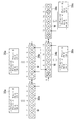
(ロット内クリーニング機能)
本機能は1ロット分のウエハWに関し、各チャンバ21において、RIE処理(以下、「製品処理」という。)(所定の処理)と洗浄処理とを連続して実行する機能である。洗浄処理とは、チャンバ21内の構成部品の表面等に付着したパーティクル等をクリーニングガスから発生させたプラズマによってエッチングする処理である。
(プロセスモジュール(PM)使用回数クリーニング機能)
本機能は複数のロット分のウエハWに関し、各チャンバ21において、製品処理を連続して実行する機能である。
(枚数指定クリーニングカウンタ継承機能)
本機能は、上述したPM使用回数クリーニング機能と同様に、複数のロット分のウエハWに関し、各チャンバ21において製品処理を連続して実行する機能であるが、各ロットのウエハWに施される製品処理の種類や連続する2つのロットにおける前のロットと後のロットの時間的間隔に応じて洗浄処理が実行されるタイミングが変化する。
(条件1)連続する2つのロットにおいて、前のロットと後のロットの時間的間隔が所定時間以内である場合
(条件2)連続する2つのロットにおいて、前のロットで実行された最後の製品処理の種類と、後のロットで実行される最初の製品処理の種類とが同じである場合
本機能では現状が上記条件1や条件2に該当するか否かを判別するために、以下に説明するロット安定ダミー処理機能を利用する。
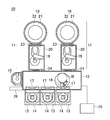
10 基板処理システム
21 チャンバ
25 システムコントローラ
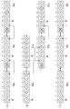
27a〜27c,28a〜28c,29a,29b,30a〜30c,31a〜31c,32a〜32c,34a〜34c ロット
33a〜33c,35a〜35c システムレシピ
Claims (5)
- 基板を収容する収容室を備え、所定の複数枚の前記基板を1ロットとして複数の前記ロットに含まれる前記基板に対して所定の処理を前記収容室において実行し、所定回数の前記基板に対する処理の後に前記収容室内の洗浄処理を実行する基板処理システムの洗浄方法であって、
前記収容室内の洗浄処理を実行するタイミングを設定するための前記基板に対する処理の実行回数を予め設定する回数設定ステップと、
前記複数のロットのロット毎に、各ロットに含まれる基板に対して実行される処理の種類及び該処理に適した前記収容室内の洗浄処理の種類を予め設定する処理設定ステップと、
前記複数のロットのうち連続する2つのロットにおいて、前のロットの基板に対して実行される処理の種類と、後のロットの基板に対して実行される処理の種類とが同じか否かを判別する種類判別ステップと、
前記前のロットの基板に対して実行される処理の種類と前記後のロットの基板に対して実行される処理の種類とが同じ場合に、前記前のロットの基板に対する処理の実行回数と前記後のロットの基板に対する処理の実行回数を累計する回数累計ステップと、
前記累計された実行回数が前記予め設定された実行回数に到達したときに、その直前に処理された基板を含むロットに対して前記処理設定ステップで設定された洗浄処理を前記収容室内に対して実行する洗浄処理実行ステップとを有することを特徴とする基板処理システムの洗浄方法。 - 前記回数累計ステップでは、前記前のロットの基板に対する処理の終了時間と前記後のロットの基板に対する処理の開始時間との間の時間的間隔が所定時間以内である場合にのみ、前記前のロットの基板に対する処理の実行回数と前記後のロットの基板に対する処理の実行回数とを累計することを特徴とする請求項1記載の基板処理システムの洗浄方法。
- 前記種類判別ステップでは、前記前のロットの基板に対する処理の名称と前記後のロットの基板に対する処理の名称とに基づいて、前記前のロットの基板に対する処理の種類と前記後のロットの基板に対する処理の種類とが同じか否かを判別することを特徴とする請求項1又は2記載の基板処理システムの洗浄方法。
- 基板を収容する収容室を備え、所定の複数枚の前記基板を1ロットとして複数の前記ロットに含まれる前記基板に対して所定の処理を前記収容室において実行し、所定回数の前記基板に対する処理の後に前記収容室内の洗浄処理を実行する基板処理システムの洗浄方法をコンピュータに実行させるプログラムを格納するコンピュータで読み取り可能な記憶媒体であって、
前記基板処理システムの洗浄方法は、
前記収容室内の洗浄処理を実行するタイミングを設定するための前記基板に対する処理の実行回数を予め設定する回数設定ステップと、
前記複数のロットのロット毎に、各ロットに含まれる基板に対して実行される処理の種類及び該処理に適した前記収容室内の洗浄処理の種類を予め設定する処理設定ステップと、
前記複数のロットのうち連続する2つのロットにおいて、前のロットの基板に対して実行される処理の種類と、後のロットの基板に対して実行される処理の種類とが同じか否かを判別する種類判別ステップと、
前記前のロットの基板に対して実行される処理の種類と前記後のロットの基板に対して実行される処理の種類とが同じ場合に、前記前のロットの基板に対する処理の実行回数と前記後のロットの基板に対する処理の実行回数を累計する回数累計ステップと、
前記累計された実行回数が前記予め設定された実行回数に到達したときに、その直前に処理された基板を含むロットに対して前記処理設定ステップで設定された洗浄処理を前記収容室内に対して実行する洗浄処理実行ステップとを有することを特徴とする記憶媒体。 - 基板を収容する収容室と、制御部とを備え、所定の複数枚の前記基板を1ロットとして複数の前記ロットに含まれる前記基板に対して所定の処理を前記収容室において実行し、所定回数の前記基板に対する処理の後に前記収容室内の洗浄処理を実行する基板処理システムであって、
前記制御部は、
前記収容室内の洗浄処理を実行するタイミングを設定するための前記基板に対する処理の実行回数を予め設定し、
前記複数のロットのロット毎に、各ロットに含まれる基板に対して実行される処理の種類及び該処理に適した前記収容室内の洗浄処理の種類を予め設定し、
前記複数のロットのうち連続する2つのロットにおいて、前のロットの基板に対して実行される処理の種類と、後のロットの基板に対して実行される処理の種類とが同じか否かを判別し、
前記前のロットの基板に対して実行される処理の種類と前記後のロットの基板に対して実行される処理の種類とが同じ場合に、前記前のロットの基板に対する処理の実行回数と前記後のロットの基板に対する処理の実行回数を累計し、
前記累計された実行回数が前記予め設定された実行回数に到達したときに、その直前に処理された基板を含むロットに対して前記設定された洗浄処理を前記収容室内に対して実行することを特徴とする基板処理システム。
Priority Applications (5)
| Application Number | Priority Date | Filing Date | Title |
|---|---|---|---|
| JP2008067806A JP5220447B2 (ja) | 2008-03-17 | 2008-03-17 | 基板処理システムの洗浄方法、記憶媒体及び基板処理システム |
| KR1020090018091A KR101227235B1 (ko) | 2008-03-17 | 2009-03-03 | 기판 처리 시스템의 세정 방법, 기억 매체 및 기판 처리 시스템 |
| US12/398,587 US8382910B2 (en) | 2008-03-17 | 2009-03-05 | Cleaning method for substrate processing system, storage medium, and substrate processing system |
| TW098108460A TWI464792B (zh) | 2008-03-17 | 2009-03-16 | Substrate processing system cleaning method, memory media and substrate processing system |
| CN2009101284480A CN101540274B (zh) | 2008-03-17 | 2009-03-17 | 基板处理系统的洗净方法和基板处理系统 |
Applications Claiming Priority (1)
| Application Number | Priority Date | Filing Date | Title |
|---|---|---|---|
| JP2008067806A JP5220447B2 (ja) | 2008-03-17 | 2008-03-17 | 基板処理システムの洗浄方法、記憶媒体及び基板処理システム |
Publications (3)
| Publication Number | Publication Date |
|---|---|
| JP2009224580A JP2009224580A (ja) | 2009-10-01 |
| JP2009224580A5 JP2009224580A5 (ja) | 2011-04-28 |
| JP5220447B2 true JP5220447B2 (ja) | 2013-06-26 |
Family
ID=41061644
Family Applications (1)
| Application Number | Title | Priority Date | Filing Date |
|---|---|---|---|
| JP2008067806A Active JP5220447B2 (ja) | 2008-03-17 | 2008-03-17 | 基板処理システムの洗浄方法、記憶媒体及び基板処理システム |
Country Status (5)
| Country | Link |
|---|---|
| US (1) | US8382910B2 (ja) |
| JP (1) | JP5220447B2 (ja) |
| KR (1) | KR101227235B1 (ja) |
| CN (1) | CN101540274B (ja) |
| TW (1) | TWI464792B (ja) |
Families Citing this family (6)
| Publication number | Priority date | Publication date | Assignee | Title |
|---|---|---|---|---|
| JP5015015B2 (ja) * | 2006-01-27 | 2012-08-29 | 株式会社日立国際電気 | 基板処理装置、レシピ表示方法、基板処理方法、半導体装置の製造方法及びレシピ遷移表示方法 |
| JP5947030B2 (ja) | 2010-12-28 | 2016-07-06 | キヤノンアネルバ株式会社 | 基板処理方法、基板処理装置 |
| CN103215572B (zh) * | 2012-01-19 | 2016-12-14 | 北京北方微电子基地设备工艺研究中心有限责任公司 | 半导体设备工艺控制方法和半导体设备工艺控制装置 |
| JP5954108B2 (ja) * | 2012-10-23 | 2016-07-20 | 東京エレクトロン株式会社 | 基板処理装置 |
| JP2016103496A (ja) * | 2014-11-27 | 2016-06-02 | 株式会社日立ハイテクノロジーズ | プラズマ処理装置 |
| CN111118458B (zh) * | 2019-12-04 | 2022-03-22 | 北京北方华创微电子装备有限公司 | 腔室清洁方法及装置 |
Family Cites Families (12)
| Publication number | Priority date | Publication date | Assignee | Title |
|---|---|---|---|---|
| JP3350264B2 (ja) * | 1994-12-22 | 2002-11-25 | 松下電器産業株式会社 | プラズマクリーニング方法 |
| JPH09298152A (ja) * | 1996-05-07 | 1997-11-18 | Nikon Corp | 加工方法 |
| JPH10135094A (ja) * | 1996-10-28 | 1998-05-22 | Canon Sales Co Inc | 半導体製造装置 |
| JPH10199817A (ja) * | 1997-01-10 | 1998-07-31 | Kokusai Electric Co Ltd | 成膜装置 |
| US6168672B1 (en) * | 1998-03-06 | 2001-01-02 | Applied Materials Inc. | Method and apparatus for automatically performing cleaning processes in a semiconductor wafer processing system |
| JP2002299315A (ja) * | 2001-03-29 | 2002-10-11 | Toshiba Corp | 半導体装置の製造方法 |
| JP4017463B2 (ja) * | 2002-07-11 | 2007-12-05 | 株式会社荏原製作所 | 洗浄方法 |
| JP2006319041A (ja) * | 2005-05-11 | 2006-11-24 | Tokyo Electron Ltd | プラズマクリーニング方法、成膜方法 |
| JP4822048B2 (ja) * | 2005-12-08 | 2011-11-24 | 富士通セミコンダクター株式会社 | 半導体製造装置のプリメンテナンス方法 |
| JP4963842B2 (ja) * | 2006-02-13 | 2012-06-27 | 東京エレクトロン株式会社 | 基板処理室の洗浄方法、記憶媒体及び基板処理装置 |
| JP4671355B2 (ja) * | 2006-03-15 | 2011-04-13 | 東京エレクトロン株式会社 | 基板処理装置のクリーニング方法,基板処理装置,プログラムを記録した記録媒体 |
| US20070215180A1 (en) * | 2006-03-15 | 2007-09-20 | Tokyo Electron Limited | Cleaning method of substrate processing equipment, substrate processing equipment, and recording medium for recording program thereof |
-
2008
- 2008-03-17 JP JP2008067806A patent/JP5220447B2/ja active Active
-
2009
- 2009-03-03 KR KR1020090018091A patent/KR101227235B1/ko active IP Right Grant
- 2009-03-05 US US12/398,587 patent/US8382910B2/en active Active
- 2009-03-16 TW TW098108460A patent/TWI464792B/zh active
- 2009-03-17 CN CN2009101284480A patent/CN101540274B/zh active Active
Also Published As
| Publication number | Publication date |
|---|---|
| KR101227235B1 (ko) | 2013-01-28 |
| US20090229635A1 (en) | 2009-09-17 |
| CN101540274B (zh) | 2012-06-13 |
| JP2009224580A (ja) | 2009-10-01 |
| TWI464792B (zh) | 2014-12-11 |
| CN101540274A (zh) | 2009-09-23 |
| KR20090099461A (ko) | 2009-09-22 |
| US8382910B2 (en) | 2013-02-26 |
| TW201003751A (en) | 2010-01-16 |
Similar Documents
| Publication | Publication Date | Title |
|---|---|---|
| JP5220447B2 (ja) | 基板処理システムの洗浄方法、記憶媒体及び基板処理システム | |
| KR101494923B1 (ko) | 고애스펙트비 구조의 식각시 마이크로로딩의 감소 방법 | |
| CN102737945B (zh) | 等离子体处理装置、等离子体处理方法 | |
| KR100845990B1 (ko) | 기판 처리 장치, 이력 정보 기록 방법, 이력 정보 기록프로그램, 및 이력 정보 기록 시스템 | |
| KR102490646B1 (ko) | 기판 처리 장치의 제어 장치 및 기판 처리 표시 방법 | |
| US20050233477A1 (en) | Substrate processing apparatus, substrate processing method, and program for implementing the method | |
| US8329050B2 (en) | Substrate processing method | |
| JP2018037559A (ja) | 基板処理方法及び基板処理システム | |
| JP5463066B2 (ja) | ロット処理開始判定方法及び制御装置 | |
| TWI728981B (zh) | 半導體製造裝置及基板運送方法 | |
| JP5323661B2 (ja) | 枚葉式の基板液処理装置における循環ラインの液交換方法 | |
| KR100856816B1 (ko) | 기판 처리 장치의 클리닝 방법, 기판 처리 장치,프로그램을 기록한 기록 매체 | |
| US20100089423A1 (en) | Cleaning method and storage medium | |
| JP2006295179A (ja) | レシピ制御オペレーションの方法 | |
| KR102364319B1 (ko) | 기판 처리 장치, 기판 처리 방법 및 기판 처리 프로그램 | |
| JP5080724B2 (ja) | 基板処理装置、基板処理方法、及びプログラム | |
| US7474934B2 (en) | Methods and apparatus for enhancing electronic device manufacturing throughput | |
| US10269605B2 (en) | Processing system and processing program | |
| CN108884566B (zh) | 异常探测系统和控制板 | |
| JP5552265B2 (ja) | 基板処理装置の制御方法及び記憶媒体 | |
| US20080190446A1 (en) | Control of dry clean process in wafer processing | |
| KR20150038995A (ko) | 기판 처리 장치의 에이징 방법 | |
| CN115812247A (zh) | 晶片状态检测 |
Legal Events
| Date | Code | Title | Description |
|---|---|---|---|
| A521 | Request for written amendment filed |
Free format text: JAPANESE INTERMEDIATE CODE: A523 Effective date: 20110310 |
|
| A621 | Written request for application examination |
Free format text: JAPANESE INTERMEDIATE CODE: A621 Effective date: 20110310 |
|
| A977 | Report on retrieval |
Free format text: JAPANESE INTERMEDIATE CODE: A971007 Effective date: 20120127 |
|
| A131 | Notification of reasons for refusal |
Free format text: JAPANESE INTERMEDIATE CODE: A131 Effective date: 20121127 |
|
| A521 | Request for written amendment filed |
Free format text: JAPANESE INTERMEDIATE CODE: A523 Effective date: 20130122 |
|
| TRDD | Decision of grant or rejection written | ||
| A01 | Written decision to grant a patent or to grant a registration (utility model) |
Free format text: JAPANESE INTERMEDIATE CODE: A01 Effective date: 20130219 |
|
| A61 | First payment of annual fees (during grant procedure) |
Free format text: JAPANESE INTERMEDIATE CODE: A61 Effective date: 20130306 |
|
| FPAY | Renewal fee payment (event date is renewal date of database) |
Free format text: PAYMENT UNTIL: 20160315 Year of fee payment: 3 |
|
| R150 | Certificate of patent or registration of utility model |
Ref document number: 5220447 Country of ref document: JP Free format text: JAPANESE INTERMEDIATE CODE: R150 Free format text: JAPANESE INTERMEDIATE CODE: R150 |
|
| R250 | Receipt of annual fees |
Free format text: JAPANESE INTERMEDIATE CODE: R250 |
|
| R250 | Receipt of annual fees |
Free format text: JAPANESE INTERMEDIATE CODE: R250 |
|
| R250 | Receipt of annual fees |
Free format text: JAPANESE INTERMEDIATE CODE: R250 |
|
| R250 | Receipt of annual fees |
Free format text: JAPANESE INTERMEDIATE CODE: R250 |
|
| R250 | Receipt of annual fees |
Free format text: JAPANESE INTERMEDIATE CODE: R250 |
|
| R250 | Receipt of annual fees |
Free format text: JAPANESE INTERMEDIATE CODE: R250 |
|
| R250 | Receipt of annual fees |
Free format text: JAPANESE INTERMEDIATE CODE: R250 |