JP4927343B2 - 半導体チップおよびその製造方法 - Google Patents
半導体チップおよびその製造方法 Download PDFInfo
- Publication number
- JP4927343B2 JP4927343B2 JP2005079105A JP2005079105A JP4927343B2 JP 4927343 B2 JP4927343 B2 JP 4927343B2 JP 2005079105 A JP2005079105 A JP 2005079105A JP 2005079105 A JP2005079105 A JP 2005079105A JP 4927343 B2 JP4927343 B2 JP 4927343B2
- Authority
- JP
- Japan
- Prior art keywords
- film
- carbon
- insulating film
- semiconductor chip
- containing insulating
- Prior art date
- Legal status (The legal status is an assumption and is not a legal conclusion. Google has not performed a legal analysis and makes no representation as to the accuracy of the status listed.)
- Expired - Fee Related
Links
Images


Classifications
-
- H—ELECTRICITY
- H10—SEMICONDUCTOR DEVICES; ELECTRIC SOLID-STATE DEVICES NOT OTHERWISE PROVIDED FOR
- H10W—GENERIC PACKAGES, INTERCONNECTIONS, CONNECTORS OR OTHER CONSTRUCTIONAL DETAILS OF DEVICES COVERED BY CLASS H10
- H10W20/00—Interconnections in chips, wafers or substrates
- H10W20/40—Interconnections external to wafers or substrates, e.g. back-end-of-line [BEOL] metallisations or vias connecting to gate electrodes
- H10W20/45—Interconnections external to wafers or substrates, e.g. back-end-of-line [BEOL] metallisations or vias connecting to gate electrodes characterised by their insulating parts
- H10W20/48—Insulating materials thereof
-
- H—ELECTRICITY
- H10—SEMICONDUCTOR DEVICES; ELECTRIC SOLID-STATE DEVICES NOT OTHERWISE PROVIDED FOR
- H10P—GENERIC PROCESSES OR APPARATUS FOR THE MANUFACTURE OR TREATMENT OF DEVICES COVERED BY CLASS H10
- H10P14/00—Formation of materials, e.g. in the shape of layers or pillars
- H10P14/60—Formation of materials, e.g. in the shape of layers or pillars of insulating materials
- H10P14/63—Formation of materials, e.g. in the shape of layers or pillars of insulating materials characterised by the formation processes
- H10P14/6326—Deposition processes
- H10P14/6328—Deposition from the gas or vapour phase
- H10P14/6334—Deposition from the gas or vapour phase using decomposition or reaction of gaseous or vapour phase compounds, i.e. chemical vapour deposition
- H10P14/6336—Deposition from the gas or vapour phase using decomposition or reaction of gaseous or vapour phase compounds, i.e. chemical vapour deposition in the presence of a plasma [PECVD]
-
- H—ELECTRICITY
- H10—SEMICONDUCTOR DEVICES; ELECTRIC SOLID-STATE DEVICES NOT OTHERWISE PROVIDED FOR
- H10P—GENERIC PROCESSES OR APPARATUS FOR THE MANUFACTURE OR TREATMENT OF DEVICES COVERED BY CLASS H10
- H10P14/00—Formation of materials, e.g. in the shape of layers or pillars
- H10P14/60—Formation of materials, e.g. in the shape of layers or pillars of insulating materials
- H10P14/65—Formation of materials, e.g. in the shape of layers or pillars of insulating materials characterised by treatments performed before or after the formation of the materials
- H10P14/6516—Formation of materials, e.g. in the shape of layers or pillars of insulating materials characterised by treatments performed before or after the formation of the materials of treatments performed after formation of the materials
- H10P14/6529—Formation of materials, e.g. in the shape of layers or pillars of insulating materials characterised by treatments performed before or after the formation of the materials of treatments performed after formation of the materials by exposure to a gas or vapour
- H10P14/6532—Formation of materials, e.g. in the shape of layers or pillars of insulating materials characterised by treatments performed before or after the formation of the materials of treatments performed after formation of the materials by exposure to a gas or vapour by exposure to a plasma
-
- H—ELECTRICITY
- H10—SEMICONDUCTOR DEVICES; ELECTRIC SOLID-STATE DEVICES NOT OTHERWISE PROVIDED FOR
- H10P—GENERIC PROCESSES OR APPARATUS FOR THE MANUFACTURE OR TREATMENT OF DEVICES COVERED BY CLASS H10
- H10P14/00—Formation of materials, e.g. in the shape of layers or pillars
- H10P14/60—Formation of materials, e.g. in the shape of layers or pillars of insulating materials
- H10P14/65—Formation of materials, e.g. in the shape of layers or pillars of insulating materials characterised by treatments performed before or after the formation of the materials
- H10P14/6516—Formation of materials, e.g. in the shape of layers or pillars of insulating materials characterised by treatments performed before or after the formation of the materials of treatments performed after formation of the materials
- H10P14/6536—Formation of materials, e.g. in the shape of layers or pillars of insulating materials characterised by treatments performed before or after the formation of the materials of treatments performed after formation of the materials by exposure to radiation, e.g. visible light
- H10P14/6538—Formation of materials, e.g. in the shape of layers or pillars of insulating materials characterised by treatments performed before or after the formation of the materials of treatments performed after formation of the materials by exposure to radiation, e.g. visible light by exposure to UV light
-
- H—ELECTRICITY
- H10—SEMICONDUCTOR DEVICES; ELECTRIC SOLID-STATE DEVICES NOT OTHERWISE PROVIDED FOR
- H10P—GENERIC PROCESSES OR APPARATUS FOR THE MANUFACTURE OR TREATMENT OF DEVICES COVERED BY CLASS H10
- H10P14/00—Formation of materials, e.g. in the shape of layers or pillars
- H10P14/60—Formation of materials, e.g. in the shape of layers or pillars of insulating materials
- H10P14/66—Formation of materials, e.g. in the shape of layers or pillars of insulating materials characterised by the type of materials
- H10P14/662—Laminate layers, e.g. stacks of alternating high-k metal oxides
-
- H—ELECTRICITY
- H10—SEMICONDUCTOR DEVICES; ELECTRIC SOLID-STATE DEVICES NOT OTHERWISE PROVIDED FOR
- H10P—GENERIC PROCESSES OR APPARATUS FOR THE MANUFACTURE OR TREATMENT OF DEVICES COVERED BY CLASS H10
- H10P14/00—Formation of materials, e.g. in the shape of layers or pillars
- H10P14/60—Formation of materials, e.g. in the shape of layers or pillars of insulating materials
- H10P14/66—Formation of materials, e.g. in the shape of layers or pillars of insulating materials characterised by the type of materials
- H10P14/668—Formation of materials, e.g. in the shape of layers or pillars of insulating materials characterised by the type of materials the materials being characterised by the deposition precursor materials
- H10P14/6681—Formation of materials, e.g. in the shape of layers or pillars of insulating materials characterised by the type of materials the materials being characterised by the deposition precursor materials the precursor containing a compound comprising Si
- H10P14/6682—Formation of materials, e.g. in the shape of layers or pillars of insulating materials characterised by the type of materials the materials being characterised by the deposition precursor materials the precursor containing a compound comprising Si the compound being a silane, e.g. disilane, methylsilane or chlorosilane
-
- H—ELECTRICITY
- H10—SEMICONDUCTOR DEVICES; ELECTRIC SOLID-STATE DEVICES NOT OTHERWISE PROVIDED FOR
- H10P—GENERIC PROCESSES OR APPARATUS FOR THE MANUFACTURE OR TREATMENT OF DEVICES COVERED BY CLASS H10
- H10P14/00—Formation of materials, e.g. in the shape of layers or pillars
- H10P14/60—Formation of materials, e.g. in the shape of layers or pillars of insulating materials
- H10P14/69—Inorganic materials
- H10P14/692—Inorganic materials composed of oxides, glassy oxides or oxide-based glasses
- H10P14/6921—Inorganic materials composed of oxides, glassy oxides or oxide-based glasses containing silicon
- H10P14/69215—Inorganic materials composed of oxides, glassy oxides or oxide-based glasses containing silicon the material being a silicon oxide, e.g. SiO2
-
- H—ELECTRICITY
- H10—SEMICONDUCTOR DEVICES; ELECTRIC SOLID-STATE DEVICES NOT OTHERWISE PROVIDED FOR
- H10P—GENERIC PROCESSES OR APPARATUS FOR THE MANUFACTURE OR TREATMENT OF DEVICES COVERED BY CLASS H10
- H10P54/00—Cutting or separating of wafers, substrates or parts of devices
-
- H—ELECTRICITY
- H10—SEMICONDUCTOR DEVICES; ELECTRIC SOLID-STATE DEVICES NOT OTHERWISE PROVIDED FOR
- H10W—GENERIC PACKAGES, INTERCONNECTIONS, CONNECTORS OR OTHER CONSTRUCTIONAL DETAILS OF DEVICES COVERED BY CLASS H10
- H10W20/00—Interconnections in chips, wafers or substrates
- H10W20/40—Interconnections external to wafers or substrates, e.g. back-end-of-line [BEOL] metallisations or vias connecting to gate electrodes
- H10W20/45—Interconnections external to wafers or substrates, e.g. back-end-of-line [BEOL] metallisations or vias connecting to gate electrodes characterised by their insulating parts
- H10W20/47—Interconnections external to wafers or substrates, e.g. back-end-of-line [BEOL] metallisations or vias connecting to gate electrodes characterised by their insulating parts comprising two or more dielectric layers having different properties, e.g. different dielectric constants
-
- H—ELECTRICITY
- H10—SEMICONDUCTOR DEVICES; ELECTRIC SOLID-STATE DEVICES NOT OTHERWISE PROVIDED FOR
- H10P—GENERIC PROCESSES OR APPARATUS FOR THE MANUFACTURE OR TREATMENT OF DEVICES COVERED BY CLASS H10
- H10P14/00—Formation of materials, e.g. in the shape of layers or pillars
- H10P14/60—Formation of materials, e.g. in the shape of layers or pillars of insulating materials
- H10P14/69—Inorganic materials
- H10P14/6903—Inorganic materials containing silicon
- H10P14/6905—Inorganic materials containing silicon being a silicon carbide or silicon carbonitride and not containing oxygen, e.g. SiC or SiC:H
-
- H—ELECTRICITY
- H10—SEMICONDUCTOR DEVICES; ELECTRIC SOLID-STATE DEVICES NOT OTHERWISE PROVIDED FOR
- H10P—GENERIC PROCESSES OR APPARATUS FOR THE MANUFACTURE OR TREATMENT OF DEVICES COVERED BY CLASS H10
- H10P14/00—Formation of materials, e.g. in the shape of layers or pillars
- H10P14/60—Formation of materials, e.g. in the shape of layers or pillars of insulating materials
- H10P14/69—Inorganic materials
- H10P14/692—Inorganic materials composed of oxides, glassy oxides or oxide-based glasses
- H10P14/6921—Inorganic materials composed of oxides, glassy oxides or oxide-based glasses containing silicon
- H10P14/6922—Inorganic materials composed of oxides, glassy oxides or oxide-based glasses containing silicon the material containing Si, O and at least one of H, N, C, F or other non-metal elements, e.g. SiOC, SiOC:H or SiONC
-
- H—ELECTRICITY
- H10—SEMICONDUCTOR DEVICES; ELECTRIC SOLID-STATE DEVICES NOT OTHERWISE PROVIDED FOR
- H10W—GENERIC PACKAGES, INTERCONNECTIONS, CONNECTORS OR OTHER CONSTRUCTIONAL DETAILS OF DEVICES COVERED BY CLASS H10
- H10W20/00—Interconnections in chips, wafers or substrates
- H10W20/40—Interconnections external to wafers or substrates, e.g. back-end-of-line [BEOL] metallisations or vias connecting to gate electrodes
- H10W20/495—Capacitive arrangements or effects of, or between wiring layers
Landscapes
- Internal Circuitry In Semiconductor Integrated Circuit Devices (AREA)
Description
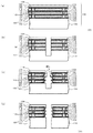
図1は、本実施の形態における半導体チップの構成の一部を示す断面図である。
半導体チップ100は、半導体基板(不図示)と、半導体基板上に形成された炭素含有絶縁膜(第一の層間絶縁膜106、第二の層間絶縁膜112、第三の層間絶縁膜118、第一のエッチングストッパ膜104、第二のエッチングストッパ膜110、第三のエッチングストッパ膜116、および第四のエッチングストッパ膜122)と炭素非含有絶縁膜(下地層102、上地カバー膜124、第一の保護絶縁膜108、第二の保護絶縁膜114、および第三の保護絶縁膜120)とを含む積層膜150とを含む。ここで、炭素非含有絶縁膜の端面が、炭素含有絶縁膜の端面より外側に位置している。
半導体チップ100は、半導体基板(不図示)と、下地層102、第一のエッチングストッパ膜104、第一の層間絶縁膜106、第一の保護絶縁膜108、第二のエッチングストッパ膜110、第二の層間絶縁膜112、第二の保護絶縁膜114、第三のエッチングストッパ膜116、第三の層間絶縁膜118、第三の保護絶縁膜120、第四のエッチングストッパ膜122、および上地カバー膜124の順で形成された積層膜150とを含む。また、半導体チップ100は、第一の配線130、ビアプラグ132、および第二の配線134を含む。
本実施の形態における半導体チップ100の製造手順は、半導体基板(不図示)上に炭素含有絶縁膜(第一の層間絶縁膜106、第二の層間絶縁膜112、第三の層間絶縁膜118、第一のエッチングストッパ膜104、第二のエッチングストッパ膜110、第三のエッチングストッパ膜116、および第四のエッチングストッパ膜122)を含む積層膜150を形成する工程(図2(a))と、半導体基板を、表面からチップ外縁に沿って切断し、炭素含有絶縁膜の側面を露出させる工程(図2(b))と、側面が露出された炭素含有絶縁膜に酸化性ガスを施し、炭素含有絶縁膜の側面を酸化する工程(図2(c))と、を含む。
まず、通常の方法により、半導体基板(不図示)上に積層膜150を形成する(図2(a))。以下に、図2(a)に示した半導体装置101の製造手順の一例を示す。まず、半導体基板上に下地層102を形成する。つづいてその上に、プラズマCVD法により、第一のエッチングストッパ膜104を成膜する。次に、第一のエッチングストッパ膜104上に、トリメチルシランガスを流しながら、プラズマCVD法により第一の層間絶縁膜106を成膜する。その後、第一の層間絶縁膜106上に、プラズマCVD法により、第一の保護絶縁膜108を形成する。つづいて、既知のリソグラフィ技術およびエッチング技術により、第一の保護絶縁膜108上に所定形状にパターニングされたレジスト膜を形成し、レジスト膜をマスクとして、第一の保護絶縁膜108、第一の層間絶縁膜106、および第一のエッチングストッパ膜104に配線溝を形成する。
酸化性ガス:O2、N2O、CO、CO2のいずれを含むガス
処理温度:室温(RT)〜400℃
処理時間:30分
酸化性ガス:O3、O2、N2O、CO、CO2のいずれを含むガス
処理温度:室温(RT)〜400℃
処理時間:5分
酸化性ガス:O2、N2O、CO、CO2のいずれか含むガス
処理温度:室温(RT)〜400℃
処理時間:5分
本実施の形態においても、半導体チップは、第一の実施の形態における半導体チップ100と同様の構成を有する。本実施の形態において、半導体チップを個別化する手順が第一の実施の形態と異なる。
本実施の形態においても、第一の実施の形態において、図2(a)を参照して説明したのと同様の手順で半導体装置101が形成される(図3(a))。
本実施の形態においても、半導体チップは、第一の実施の形態における半導体チップ100と同様の構成を有する。本実施の形態において、半導体チップを個別化および酸化処理する手順が第一の実施の形態と異なる。
本実施の形態においても、第一の実施の形態において、図2(a)を参照して説明したのと同様の手順で半導体装置101が形成される(図4(a))。つづいて、ブレードダイシング、レーザダイシング、またはリソグラフィおよびドライエッチング技術により、半導体装置101を半導体基板の表面からチップ外縁に沿って切断するとともに、酸化性ガスを施し、酸化処理を行う(図4(b))。これにより、半導体装置101の積層膜150の側面が酸化される。酸化処理の条件は、第一の実施の形態と同様とすることができる。
第一の実施の形態で図2(a)を参照して説明した手順の一部と同様にして、半導体チップを製造した。まず、半導体基板上に下地絶縁膜を設け、その上にプラズマCVD法により、SiCN膜(膜厚50nm)を形成した。その後、SiCN膜上にプラズマCVD法により、SiOC膜(膜厚300nm)を形成した。つづいて、SiCN膜上にプラズマCVD法により、SiO2膜(膜厚100nm)を形成した。その後、SiO2膜上にレジスト膜を形成し、リソグラフィ技術およびエッチング技術により、配線溝を形成した。つづいて、レジスト膜を除去した。次いで、配線溝内にスパッタリング法によりTa/TaN膜を形成した。その後、バリア膜上において、配線溝を埋め込むように、電解めっき法により配線金属膜を形成した。つづいて、配線溝外部に形成された不要な配線金属膜およびバリア膜をCMPにより除去し、その上にSiO2膜を形成し、半導体装置を製造した。
例1と同様の手順で半導体装置を製造した後、半導体装置を大気中で常温で切断して半導体チップを個別化した。
炭素組成は、断面TEMのEDX(エネルギー分散型蛍光X線分析装置: Energy Dispersive X-Ray Fluorescence spectroscopy)分析により、炭素(C)とケイ素(Si)の強度比を測定することにより算出した。
102 下地層
104 第一のエッチングストッパ膜
106 第一の層間絶縁膜
108 第一の保護絶縁膜
110 第二のエッチングストッパ膜
112 第二の層間絶縁膜
114 第二の保護絶縁膜
116 第三のエッチングストッパ膜
118 第三の層間絶縁膜
120 第三の保護絶縁膜
122 第四のエッチングストッパ膜
124 上地カバー膜
130 第一の配線
132 ビアプラグ
134 第二の配線
Claims (18)
- 半導体基板と、
前記半導体基板上に形成された炭素含有絶縁膜と炭素非含有絶縁膜とを含む積層膜と、
を含み、
前記炭素非含有絶縁膜の端面が、前記炭素含有絶縁膜の端面より外側に位置しており、
前記炭素含有絶縁膜は、エッチングストッパ膜、および前記エッチングストッパ膜上に設けられた比誘電率が3.3以下の低誘電率膜を含み、
側面の一部が、前記炭素含有絶縁膜の端面および前記炭素非含有絶縁膜の端面により構成されていることを特徴とする半導体チップ。 - 請求項1に記載の半導体チップにおいて、
前記炭素含有絶縁膜は、端部における炭素の組成が、内部における炭素の組成よりも低いことを特徴とする半導体チップ。 - 請求項1または2に記載の半導体チップにおいて、
前記炭素含有絶縁膜は、端部近傍において、内部に向かうにつれ炭素の組成が高くなる領域を含むことを特徴とする半導体チップ。 - 請求項1乃至3いずれかに記載の半導体チップにおいて、
前記炭素含有絶縁膜は、端部における膜密度が、内部における膜密度よりも高いことを特徴とする半導体チップ。 - 請求項1乃至4いずれかに記載の半導体チップにおいて、
前記炭素含有絶縁膜は、端部近傍において、内部に向かうにつれ膜密度が低くなる領域を含むことを特徴とする半導体チップ。 - 請求項1乃至5いずれかに記載の半導体チップにおいて、
前記エッチングストッパ膜は、SiCN、またはSiCにより構成されることを特徴とする半導体チップ。 - 請求項1乃至6いずれかに記載の半導体チップにおいて、
前記低誘電率膜は、SiOC、メチルシルセスキオキサン、水素化メチルシルセスキオキサン、または有機ポリシロキサン、もしくはこれらの膜をポーラス化したものにより構成されることを特徴とする半導体チップ。 - 半導体基板と、
前記半導体基板上に形成された炭素含有絶縁膜を含む積層膜と、
を含み、
前記炭素含有絶縁膜は、端部における炭素の組成が、内部における炭素の組成よりも低く、
前記炭素含有絶縁膜は、エッチングストッパ膜、および前記エッチングストッパ膜上に設けられた比誘電率が3.3以下の低誘電率膜を含み、
側面の一部が、前記炭素含有絶縁膜の端面により構成されていることを特徴とする半導体チップ。 - 請求項8に記載の半導体チップにおいて、
前記炭素含有絶縁膜は、端部近傍において、内部に向かうにつれ炭素の組成が高くなる領域を含むことを特徴とする半導体チップ。 - 請求項8または9に記載の半導体チップにおいて、
前記低誘電率膜は、SiOC、メチルシルセスキオキサン、水素化メチルシルセスキオキサン、または有機ポリシロキサン、もしくはこれらの膜をポーラス化したものにより構成されることを特徴とする半導体チップ。 - 請求項8乃至10いずれかに記載の半導体チップにおいて、
前記エッチングストッパ膜は、SiCN、またはSiCにより構成されることを特徴とする半導体チップ。 - 半導体基板と、
前記半導体基板上に形成された炭素含有絶縁膜を含む積層膜と、
を含み、
前記炭素含有絶縁膜は、端部における膜密度が、内部における膜密度よりも高く、
前記炭素含有絶縁膜は、エッチングストッパ膜、および前記エッチングストッパ膜上に設けられた比誘電率が3.3以下の低誘電率膜を含み、
側面の一部が、前記炭素含有絶縁膜の端面により構成されていることを特徴とする半導体チップ。 - 請求項12に記載の半導体チップにおいて、
前記炭素含有絶縁膜は、端部近傍において、内部に向かうにつれ膜密度が低くなる領域を含むことを特徴とする半導体チップ。 - 請求項12または13に記載の半導体チップにおいて、
前記低誘電率膜は、SiOC、メチルシルセスキオキサン、水素化メチルシルセスキオキサン、または有機ポリシロキサン、もしくはこれらの膜をポーラス化したものにより構成されることを特徴とする半導体チップ。 - 請求項12乃至14いずれかに記載の半導体チップにおいて、
前記エッチングストッパ膜は、SiCN、またはSiCにより構成されることを特徴とする半導体チップ。 - 請求項1乃至15いずれかに記載の半導体チップにおいて、
前記半導体基板の側面は酸化されていない半導体チップ。 - 半導体基板上に炭素含有絶縁膜を含む積層膜を形成する工程と、
前記半導体基板の表面側からチップ外縁に沿って少なくとも前記炭素含有絶縁膜を切断し、前記炭素含有絶縁膜の側面を露出させる工程と、
側面が露出された前記炭素含有絶縁膜に酸化性ガスを施し、前記炭素含有絶縁膜の前記側面を酸化する工程と、
を含み、
前記炭素含有絶縁膜は、エッチングストッパ膜、および前記エッチングストッパ膜上に設けられた比誘電率が3.3以下の低誘電率膜を含むことを特徴とする半導体チップの製造方法。 - 請求項17に記載の半導体チップの製造方法において、
前記炭素含有絶縁膜の側面を露出させる工程において、前記半導体基板には切り込みは入れられず、
前記炭素含有絶縁膜の前記側面を酸化する工程の後に、前記半導体基板を切断する工程を備える半導体チップの製造方法。
Priority Applications (4)
| Application Number | Priority Date | Filing Date | Title |
|---|---|---|---|
| JP2005079105A JP4927343B2 (ja) | 2005-03-18 | 2005-03-18 | 半導体チップおよびその製造方法 |
| US11/368,671 US7564132B2 (en) | 2005-03-18 | 2006-03-07 | Semiconductor chip |
| CNB2006100714026A CN100550366C (zh) | 2005-03-18 | 2006-03-20 | 半导体芯片 |
| CN2008100921542A CN101276803B (zh) | 2005-03-18 | 2006-03-20 | 半导体芯片 |
Applications Claiming Priority (1)
| Application Number | Priority Date | Filing Date | Title |
|---|---|---|---|
| JP2005079105A JP4927343B2 (ja) | 2005-03-18 | 2005-03-18 | 半導体チップおよびその製造方法 |
Publications (2)
| Publication Number | Publication Date |
|---|---|
| JP2006261514A JP2006261514A (ja) | 2006-09-28 |
| JP4927343B2 true JP4927343B2 (ja) | 2012-05-09 |
Family
ID=37002908
Family Applications (1)
| Application Number | Title | Priority Date | Filing Date |
|---|---|---|---|
| JP2005079105A Expired - Fee Related JP4927343B2 (ja) | 2005-03-18 | 2005-03-18 | 半導体チップおよびその製造方法 |
Country Status (3)
| Country | Link |
|---|---|
| US (1) | US7564132B2 (ja) |
| JP (1) | JP4927343B2 (ja) |
| CN (2) | CN101276803B (ja) |
Families Citing this family (2)
| Publication number | Priority date | Publication date | Assignee | Title |
|---|---|---|---|---|
| JP4786518B2 (ja) * | 2006-12-19 | 2011-10-05 | 株式会社東芝 | 半導体装置の製造方法 |
| CN107665829B (zh) * | 2017-08-24 | 2019-12-17 | 长江存储科技有限责任公司 | 晶圆混合键合中提高金属引线制程安全性的方法 |
Family Cites Families (17)
| Publication number | Priority date | Publication date | Assignee | Title |
|---|---|---|---|---|
| JPH01225333A (ja) * | 1988-03-04 | 1989-09-08 | Nec Corp | 半導体装置の製造方法 |
| US5293073A (en) * | 1989-06-27 | 1994-03-08 | Kabushiki Kaisha Toshiba | Electrode structure of a semiconductor device which uses a copper wire as a bonding wire |
| JP2561039B2 (ja) * | 1994-11-22 | 1996-12-04 | 日本電気株式会社 | 半導体チップおよび回路基板の接続方法 |
| US6340435B1 (en) * | 1998-02-11 | 2002-01-22 | Applied Materials, Inc. | Integrated low K dielectrics and etch stops |
| JP4361625B2 (ja) * | 1998-10-05 | 2009-11-11 | 東京エレクトロン株式会社 | 半導体装置及びその製造方法 |
| DE19848460A1 (de) * | 1998-10-21 | 2000-05-04 | Micronas Intermetall Gmbh | Halbleiterbauelement und Verfahren zum Herstellen eines Halbleiterchips |
| JP2000133710A (ja) * | 1998-10-26 | 2000-05-12 | Tokyo Electron Ltd | 半導体装置及びその製造方法 |
| JP2001308037A (ja) * | 2000-04-26 | 2001-11-02 | Seiko Epson Corp | ダイシング方法 |
| JP2002026121A (ja) * | 2000-06-30 | 2002-01-25 | Tokyo Electron Ltd | 半導体装置およびその製造方法、絶縁膜の形成方法 |
| JP2002203899A (ja) | 2000-12-28 | 2002-07-19 | Matsushita Electric Ind Co Ltd | 銅相互接続構造の形成方法 |
| JP4160277B2 (ja) | 2001-06-29 | 2008-10-01 | 株式会社東芝 | 半導体装置の製造方法 |
| CN1261998C (zh) * | 2002-09-03 | 2006-06-28 | 株式会社东芝 | 半导体器件 |
| JP2004134450A (ja) * | 2002-10-08 | 2004-04-30 | Fujitsu Ltd | 半導体集積回路 |
| JP2004179302A (ja) | 2002-11-26 | 2004-06-24 | Disco Abrasive Syst Ltd | 半導体ウエーハの分割方法 |
| JP4086673B2 (ja) * | 2003-02-04 | 2008-05-14 | Necエレクトロニクス株式会社 | 半導体装置及びその製造方法 |
| WO2004097916A1 (ja) * | 2003-04-30 | 2004-11-11 | Fujitsu Limited | 半導体装置の製造方法、半導体ウエハおよび半導体装置 |
| JP2006228865A (ja) * | 2005-02-16 | 2006-08-31 | Seiko Epson Corp | 半導体装置及びその製造方法 |
-
2005
- 2005-03-18 JP JP2005079105A patent/JP4927343B2/ja not_active Expired - Fee Related
-
2006
- 2006-03-07 US US11/368,671 patent/US7564132B2/en not_active Expired - Fee Related
- 2006-03-20 CN CN2008100921542A patent/CN101276803B/zh not_active Expired - Fee Related
- 2006-03-20 CN CNB2006100714026A patent/CN100550366C/zh not_active Expired - Fee Related
Also Published As
| Publication number | Publication date |
|---|---|
| CN100550366C (zh) | 2009-10-14 |
| US20060208361A1 (en) | 2006-09-21 |
| CN101276803A (zh) | 2008-10-01 |
| JP2006261514A (ja) | 2006-09-28 |
| CN101276803B (zh) | 2010-12-01 |
| CN1835225A (zh) | 2006-09-20 |
| US7564132B2 (en) | 2009-07-21 |
Similar Documents
| Publication | Publication Date | Title |
|---|---|---|
| JP5204370B2 (ja) | 半導体装置およびその製造方法 | |
| JP5180426B2 (ja) | 半導体装置の製造方法 | |
| JP4328725B2 (ja) | 改良された信頼性を有する超低誘電率(k)誘電体を集積化する構造および方法 | |
| KR100516337B1 (ko) | 반도체 디바이스 및 그 제조 방법 | |
| US8455985B2 (en) | Integrated circuit devices having selectively strengthened composite interlayer insulation layers and methods of fabricating the same | |
| JP2010171081A (ja) | 半導体装置及びその製造方法 | |
| JP2007227720A (ja) | 半導体装置とその製造方法 | |
| JP5380838B2 (ja) | 半導体装置の製造方法 | |
| US20060099802A1 (en) | Diffusion barrier for damascene structures | |
| JP2004235548A (ja) | 半導体装置およびその製造方法 | |
| US8390135B2 (en) | Semiconductor device | |
| TWI413212B (zh) | 半導體裝置及其製造方法 | |
| JP5060037B2 (ja) | 半導体装置の製造方法 | |
| JP4675258B2 (ja) | 半導体装置の製造方法および半導体装置 | |
| JP4567587B2 (ja) | 半導体装置の製造方法 | |
| JP4419025B2 (ja) | 半導体装置の製造方法 | |
| JP4927343B2 (ja) | 半導体チップおよびその製造方法 | |
| JP5200436B2 (ja) | 半導体装置の製造方法 | |
| JP2005217319A (ja) | 多層配線構造、半導体装置及び半導体実装装置 | |
| JP2009117739A (ja) | 電子装置及びその製造方法 | |
| JP2006319116A (ja) | 半導体装置およびその製造方法 | |
| JP2005217320A (ja) | 配線形成方法、半導体装置の製造方法並びに半導体実装装置の製造方法 | |
| JP2006140373A (ja) | 半導体装置の製造方法 | |
| JP5408116B2 (ja) | 半導体装置の製造方法 | |
| JP2010245156A (ja) | 半導体装置の製造方法 |
Legal Events
| Date | Code | Title | Description |
|---|---|---|---|
| A621 | Written request for application examination |
Free format text: JAPANESE INTERMEDIATE CODE: A621 Effective date: 20080215 |
|
| A977 | Report on retrieval |
Free format text: JAPANESE INTERMEDIATE CODE: A971007 Effective date: 20100401 |
|
| A131 | Notification of reasons for refusal |
Free format text: JAPANESE INTERMEDIATE CODE: A131 Effective date: 20110920 |
|
| A521 | Request for written amendment filed |
Free format text: JAPANESE INTERMEDIATE CODE: A523 Effective date: 20111121 |
|
| TRDD | Decision of grant or rejection written | ||
| A01 | Written decision to grant a patent or to grant a registration (utility model) |
Free format text: JAPANESE INTERMEDIATE CODE: A01 Effective date: 20120207 |
|
| A01 | Written decision to grant a patent or to grant a registration (utility model) |
Free format text: JAPANESE INTERMEDIATE CODE: A01 |
|
| A61 | First payment of annual fees (during grant procedure) |
Free format text: JAPANESE INTERMEDIATE CODE: A61 Effective date: 20120209 |
|
| FPAY | Renewal fee payment (event date is renewal date of database) |
Free format text: PAYMENT UNTIL: 20150217 Year of fee payment: 3 |
|
| R150 | Certificate of patent or registration of utility model |
Free format text: JAPANESE INTERMEDIATE CODE: R150 |
|
| S531 | Written request for registration of change of domicile |
Free format text: JAPANESE INTERMEDIATE CODE: R313531 |
|
| R350 | Written notification of registration of transfer |
Free format text: JAPANESE INTERMEDIATE CODE: R350 |
|
| LAPS | Cancellation because of no payment of annual fees |