JP4817636B2 - 半導体装置およびその作製方法 - Google Patents
半導体装置およびその作製方法 Download PDFInfo
- Publication number
- JP4817636B2 JP4817636B2 JP2004291554A JP2004291554A JP4817636B2 JP 4817636 B2 JP4817636 B2 JP 4817636B2 JP 2004291554 A JP2004291554 A JP 2004291554A JP 2004291554 A JP2004291554 A JP 2004291554A JP 4817636 B2 JP4817636 B2 JP 4817636B2
- Authority
- JP
- Japan
- Prior art keywords
- electrode
- film
- wiring
- photoelectric conversion
- forming
- Prior art date
- Legal status (The legal status is an assumption and is not a legal conclusion. Google has not performed a legal analysis and makes no representation as to the accuracy of the status listed.)
- Expired - Fee Related
Links
- 239000004065 semiconductor Substances 0.000 title claims description 131
- 238000004519 manufacturing process Methods 0.000 title claims description 19
- 239000010408 film Substances 0.000 claims description 266
- 238000000034 method Methods 0.000 claims description 85
- 239000000758 substrate Substances 0.000 claims description 85
- 238000006243 chemical reaction Methods 0.000 claims description 56
- 238000007639 printing Methods 0.000 claims description 27
- 238000005530 etching Methods 0.000 claims description 26
- 239000011521 glass Substances 0.000 claims description 25
- 238000007789 sealing Methods 0.000 claims description 17
- 239000004033 plastic Substances 0.000 claims description 15
- 229920003023 plastic Polymers 0.000 claims description 15
- 239000010409 thin film Substances 0.000 claims description 14
- 230000015572 biosynthetic process Effects 0.000 claims description 12
- 229910052782 aluminium Inorganic materials 0.000 claims description 10
- XAGFODPZIPBFFR-UHFFFAOYSA-N aluminium Chemical compound [Al] XAGFODPZIPBFFR-UHFFFAOYSA-N 0.000 claims description 10
- 239000010410 layer Substances 0.000 description 166
- 230000003287 optical effect Effects 0.000 description 58
- 229910052751 metal Inorganic materials 0.000 description 41
- 239000002184 metal Substances 0.000 description 41
- 229910021417 amorphous silicon Inorganic materials 0.000 description 24
- 239000010936 titanium Substances 0.000 description 24
- 230000008569 process Effects 0.000 description 21
- 239000013078 crystal Substances 0.000 description 19
- 239000007789 gas Substances 0.000 description 18
- 238000007650 screen-printing Methods 0.000 description 18
- 238000010438 heat treatment Methods 0.000 description 17
- 239000000853 adhesive Substances 0.000 description 16
- 230000001070 adhesive effect Effects 0.000 description 16
- 239000000463 material Substances 0.000 description 16
- 229910000679 solder Inorganic materials 0.000 description 15
- PXHVJJICTQNCMI-UHFFFAOYSA-N Nickel Chemical compound [Ni] PXHVJJICTQNCMI-UHFFFAOYSA-N 0.000 description 14
- XUIMIQQOPSSXEZ-UHFFFAOYSA-N Silicon Chemical compound [Si] XUIMIQQOPSSXEZ-UHFFFAOYSA-N 0.000 description 13
- 229910052739 hydrogen Inorganic materials 0.000 description 13
- 229910021420 polycrystalline silicon Inorganic materials 0.000 description 13
- 229920005591 polysilicon Polymers 0.000 description 13
- 229910052710 silicon Inorganic materials 0.000 description 13
- 239000010703 silicon Substances 0.000 description 13
- XKRFYHLGVUSROY-UHFFFAOYSA-N Argon Chemical compound [Ar] XKRFYHLGVUSROY-UHFFFAOYSA-N 0.000 description 12
- 239000001257 hydrogen Substances 0.000 description 12
- 229920005989 resin Polymers 0.000 description 12
- 239000011347 resin Substances 0.000 description 12
- 230000004888 barrier function Effects 0.000 description 11
- 239000011229 interlayer Substances 0.000 description 11
- UFHFLCQGNIYNRP-UHFFFAOYSA-N Hydrogen Chemical compound [H][H] UFHFLCQGNIYNRP-UHFFFAOYSA-N 0.000 description 9
- 229910021421 monocrystalline silicon Inorganic materials 0.000 description 9
- 238000004544 sputter deposition Methods 0.000 description 9
- 239000002585 base Substances 0.000 description 8
- 239000004020 conductor Substances 0.000 description 8
- 238000005247 gettering Methods 0.000 description 8
- 229910044991 metal oxide Inorganic materials 0.000 description 8
- 150000004706 metal oxides Chemical class 0.000 description 8
- VYPSYNLAJGMNEJ-UHFFFAOYSA-N Silicium dioxide Chemical compound O=[Si]=O VYPSYNLAJGMNEJ-UHFFFAOYSA-N 0.000 description 7
- 238000002425 crystallisation Methods 0.000 description 7
- 238000010586 diagram Methods 0.000 description 7
- 229910052760 oxygen Inorganic materials 0.000 description 7
- 229910052814 silicon oxide Inorganic materials 0.000 description 7
- KRHYYFGTRYWZRS-UHFFFAOYSA-N Fluorane Chemical compound F KRHYYFGTRYWZRS-UHFFFAOYSA-N 0.000 description 6
- 229910052786 argon Inorganic materials 0.000 description 6
- QVGXLLKOCUKJST-UHFFFAOYSA-N atomic oxygen Chemical compound [O] QVGXLLKOCUKJST-UHFFFAOYSA-N 0.000 description 6
- 239000012535 impurity Substances 0.000 description 6
- 229910052759 nickel Inorganic materials 0.000 description 6
- 239000001301 oxygen Substances 0.000 description 6
- -1 siloxane structure Chemical group 0.000 description 6
- 238000005229 chemical vapour deposition Methods 0.000 description 5
- 230000008025 crystallization Effects 0.000 description 5
- 238000001312 dry etching Methods 0.000 description 5
- 229910021424 microcrystalline silicon Inorganic materials 0.000 description 5
- 150000004767 nitrides Chemical class 0.000 description 5
- 230000035945 sensitivity Effects 0.000 description 5
- 230000006866 deterioration Effects 0.000 description 4
- 238000009792 diffusion process Methods 0.000 description 4
- PCHJSUWPFVWCPO-UHFFFAOYSA-N gold Chemical compound [Au] PCHJSUWPFVWCPO-UHFFFAOYSA-N 0.000 description 4
- 239000011810 insulating material Substances 0.000 description 4
- 229910052750 molybdenum Inorganic materials 0.000 description 4
- 238000005268 plasma chemical vapour deposition Methods 0.000 description 4
- 239000002985 plastic film Substances 0.000 description 4
- 229920006255 plastic film Polymers 0.000 description 4
- 238000012545 processing Methods 0.000 description 4
- 239000002356 single layer Substances 0.000 description 4
- 229910052719 titanium Inorganic materials 0.000 description 4
- 229910052721 tungsten Inorganic materials 0.000 description 4
- XLYOFNOQVPJJNP-UHFFFAOYSA-N water Substances O XLYOFNOQVPJJNP-UHFFFAOYSA-N 0.000 description 4
- CBENFWSGALASAD-UHFFFAOYSA-N Ozone Chemical compound [O-][O+]=O CBENFWSGALASAD-UHFFFAOYSA-N 0.000 description 3
- 229910052581 Si3N4 Inorganic materials 0.000 description 3
- 239000000956 alloy Substances 0.000 description 3
- 230000003321 amplification Effects 0.000 description 3
- 238000005452 bending Methods 0.000 description 3
- 230000003197 catalytic effect Effects 0.000 description 3
- 230000005684 electric field Effects 0.000 description 3
- 150000002431 hydrogen Chemical class 0.000 description 3
- 238000002347 injection Methods 0.000 description 3
- 239000007924 injection Substances 0.000 description 3
- 238000003199 nucleic acid amplification method Methods 0.000 description 3
- 238000000926 separation method Methods 0.000 description 3
- HQVNEWCFYHHQES-UHFFFAOYSA-N silicon nitride Chemical compound N12[Si]34N5[Si]62N3[Si]51N64 HQVNEWCFYHHQES-UHFFFAOYSA-N 0.000 description 3
- 238000012546 transfer Methods 0.000 description 3
- 239000010937 tungsten Substances 0.000 description 3
- OKTJSMMVPCPJKN-UHFFFAOYSA-N Carbon Chemical compound [C] OKTJSMMVPCPJKN-UHFFFAOYSA-N 0.000 description 2
- 239000004721 Polyphenylene oxide Substances 0.000 description 2
- 239000004743 Polypropylene Substances 0.000 description 2
- 229910004298 SiO 2 Inorganic materials 0.000 description 2
- UCKMPCXJQFINFW-UHFFFAOYSA-N Sulphide Chemical compound [S-2] UCKMPCXJQFINFW-UHFFFAOYSA-N 0.000 description 2
- 229910045601 alloy Inorganic materials 0.000 description 2
- AZDRQVAHHNSJOQ-UHFFFAOYSA-N alumane Chemical group [AlH3] AZDRQVAHHNSJOQ-UHFFFAOYSA-N 0.000 description 2
- 229910052799 carbon Inorganic materials 0.000 description 2
- 238000000576 coating method Methods 0.000 description 2
- 150000001875 compounds Chemical class 0.000 description 2
- 238000012937 correction Methods 0.000 description 2
- 238000000151 deposition Methods 0.000 description 2
- 230000000694 effects Effects 0.000 description 2
- 239000010931 gold Substances 0.000 description 2
- 238000005286 illumination Methods 0.000 description 2
- 238000009616 inductively coupled plasma Methods 0.000 description 2
- 239000004973 liquid crystal related substance Substances 0.000 description 2
- QGLKJKCYBOYXKC-UHFFFAOYSA-N nonaoxidotritungsten Chemical compound O=[W]1(=O)O[W](=O)(=O)O[W](=O)(=O)O1 QGLKJKCYBOYXKC-UHFFFAOYSA-N 0.000 description 2
- 238000000059 patterning Methods 0.000 description 2
- 229920003207 poly(ethylene-2,6-naphthalate) Polymers 0.000 description 2
- 229920001690 polydopamine Polymers 0.000 description 2
- 239000011112 polyethylene naphthalate Substances 0.000 description 2
- 229920000139 polyethylene terephthalate Polymers 0.000 description 2
- 239000005020 polyethylene terephthalate Substances 0.000 description 2
- 229920001155 polypropylene Polymers 0.000 description 2
- 230000002040 relaxant effect Effects 0.000 description 2
- WFKWXMTUELFFGS-UHFFFAOYSA-N tungsten Chemical compound [W] WFKWXMTUELFFGS-UHFFFAOYSA-N 0.000 description 2
- 229910001930 tungsten oxide Inorganic materials 0.000 description 2
- 238000001039 wet etching Methods 0.000 description 2
- 229910000838 Al alloy Inorganic materials 0.000 description 1
- ZOXJGFHDIHLPTG-UHFFFAOYSA-N Boron Chemical compound [B] ZOXJGFHDIHLPTG-UHFFFAOYSA-N 0.000 description 1
- 229910052779 Neodymium Inorganic materials 0.000 description 1
- OAICVXFJPJFONN-UHFFFAOYSA-N Phosphorus Chemical compound [P] OAICVXFJPJFONN-UHFFFAOYSA-N 0.000 description 1
- 239000004697 Polyetherimide Substances 0.000 description 1
- 239000004734 Polyphenylene sulfide Substances 0.000 description 1
- 239000004954 Polyphthalamide Substances 0.000 description 1
- BLRPTPMANUNPDV-UHFFFAOYSA-N Silane Chemical compound [SiH4] BLRPTPMANUNPDV-UHFFFAOYSA-N 0.000 description 1
- 229910000577 Silicon-germanium Inorganic materials 0.000 description 1
- 229910000831 Steel Inorganic materials 0.000 description 1
- NRTOMJZYCJJWKI-UHFFFAOYSA-N Titanium nitride Chemical compound [Ti]#N NRTOMJZYCJJWKI-UHFFFAOYSA-N 0.000 description 1
- LEVVHYCKPQWKOP-UHFFFAOYSA-N [Si].[Ge] Chemical compound [Si].[Ge] LEVVHYCKPQWKOP-UHFFFAOYSA-N 0.000 description 1
- 238000002679 ablation Methods 0.000 description 1
- 230000003213 activating effect Effects 0.000 description 1
- 230000004913 activation Effects 0.000 description 1
- 229910052783 alkali metal Inorganic materials 0.000 description 1
- 150000001340 alkali metals Chemical class 0.000 description 1
- 238000000137 annealing Methods 0.000 description 1
- 238000013459 approach Methods 0.000 description 1
- GPBUGPUPKAGMDK-UHFFFAOYSA-N azanylidynemolybdenum Chemical compound [Mo]#N GPBUGPUPKAGMDK-UHFFFAOYSA-N 0.000 description 1
- 230000008901 benefit Effects 0.000 description 1
- 230000000903 blocking effect Effects 0.000 description 1
- 229910052796 boron Inorganic materials 0.000 description 1
- 239000000969 carrier Substances 0.000 description 1
- 230000001413 cellular effect Effects 0.000 description 1
- 229910052804 chromium Inorganic materials 0.000 description 1
- 239000011248 coating agent Substances 0.000 description 1
- 230000007547 defect Effects 0.000 description 1
- 230000000593 degrading effect Effects 0.000 description 1
- 230000008021 deposition Effects 0.000 description 1
- 238000001514 detection method Methods 0.000 description 1
- ZOCHARZZJNPSEU-UHFFFAOYSA-N diboron Chemical compound B#B ZOCHARZZJNPSEU-UHFFFAOYSA-N 0.000 description 1
- 230000007613 environmental effect Effects 0.000 description 1
- 239000000835 fiber Substances 0.000 description 1
- 229910052737 gold Inorganic materials 0.000 description 1
- 238000003384 imaging method Methods 0.000 description 1
- 230000006872 improvement Effects 0.000 description 1
- 239000011261 inert gas Substances 0.000 description 1
- 150000002500 ions Chemical class 0.000 description 1
- 229910052741 iridium Inorganic materials 0.000 description 1
- 229910052742 iron Inorganic materials 0.000 description 1
- 230000001678 irradiating effect Effects 0.000 description 1
- 238000005499 laser crystallization Methods 0.000 description 1
- 239000012528 membrane Substances 0.000 description 1
- 239000005300 metallic glass Substances 0.000 description 1
- 150000002739 metals Chemical class 0.000 description 1
- 239000000203 mixture Substances 0.000 description 1
- AIYYMMQIMJOTBM-UHFFFAOYSA-L nickel(ii) acetate Chemical compound [Ni+2].CC([O-])=O.CC([O-])=O AIYYMMQIMJOTBM-UHFFFAOYSA-L 0.000 description 1
- 229910052757 nitrogen Inorganic materials 0.000 description 1
- 239000011368 organic material Substances 0.000 description 1
- 229910052762 osmium Inorganic materials 0.000 description 1
- 230000001590 oxidative effect Effects 0.000 description 1
- 229910052763 palladium Inorganic materials 0.000 description 1
- 229910052698 phosphorus Inorganic materials 0.000 description 1
- 239000011574 phosphorus Substances 0.000 description 1
- 238000009832 plasma treatment Methods 0.000 description 1
- 238000005498 polishing Methods 0.000 description 1
- 229920002492 poly(sulfone) Polymers 0.000 description 1
- 239000004417 polycarbonate Substances 0.000 description 1
- 229920000515 polycarbonate Polymers 0.000 description 1
- 229920000570 polyether Polymers 0.000 description 1
- 229920001601 polyetherimide Polymers 0.000 description 1
- 229920000642 polymer Polymers 0.000 description 1
- 229920006380 polyphenylene oxide Polymers 0.000 description 1
- 229920000069 polyphenylene sulfide Polymers 0.000 description 1
- 229920006375 polyphtalamide Polymers 0.000 description 1
- 239000010453 quartz Substances 0.000 description 1
- 238000004151 rapid thermal annealing Methods 0.000 description 1
- 239000003870 refractory metal Substances 0.000 description 1
- 230000007261 regionalization Effects 0.000 description 1
- 229910052703 rhodium Inorganic materials 0.000 description 1
- 229910052707 ruthenium Inorganic materials 0.000 description 1
- 239000012266 salt solution Substances 0.000 description 1
- 239000003566 sealing material Substances 0.000 description 1
- 229910052709 silver Inorganic materials 0.000 description 1
- 239000004332 silver Substances 0.000 description 1
- 239000007790 solid phase Substances 0.000 description 1
- 239000010959 steel Substances 0.000 description 1
- 230000001629 suppression Effects 0.000 description 1
- 238000010301 surface-oxidation reaction Methods 0.000 description 1
- 229920003002 synthetic resin Polymers 0.000 description 1
- 239000000057 synthetic resin Substances 0.000 description 1
- 229910052715 tantalum Inorganic materials 0.000 description 1
- MZLGASXMSKOWSE-UHFFFAOYSA-N tantalum nitride Chemical compound [Ta]#N MZLGASXMSKOWSE-UHFFFAOYSA-N 0.000 description 1
- 238000002230 thermal chemical vapour deposition Methods 0.000 description 1
- 229920001187 thermosetting polymer Polymers 0.000 description 1
- 238000002834 transmittance Methods 0.000 description 1
- 238000007740 vapor deposition Methods 0.000 description 1
- 229910052725 zinc Inorganic materials 0.000 description 1
- 229910052726 zirconium Inorganic materials 0.000 description 1
Images


Classifications
-
- H—ELECTRICITY
- H01—ELECTRIC ELEMENTS
- H01L—SEMICONDUCTOR DEVICES NOT COVERED BY CLASS H10
- H01L27/00—Devices consisting of a plurality of semiconductor or other solid-state components formed in or on a common substrate
- H01L27/02—Devices consisting of a plurality of semiconductor or other solid-state components formed in or on a common substrate including semiconductor components specially adapted for rectifying, oscillating, amplifying or switching and having at least one potential-jump barrier or surface barrier; including integrated passive circuit elements with at least one potential-jump barrier or surface barrier
- H01L27/12—Devices consisting of a plurality of semiconductor or other solid-state components formed in or on a common substrate including semiconductor components specially adapted for rectifying, oscillating, amplifying or switching and having at least one potential-jump barrier or surface barrier; including integrated passive circuit elements with at least one potential-jump barrier or surface barrier the substrate being other than a semiconductor body, e.g. an insulating body
- H01L27/1214—Devices consisting of a plurality of semiconductor or other solid-state components formed in or on a common substrate including semiconductor components specially adapted for rectifying, oscillating, amplifying or switching and having at least one potential-jump barrier or surface barrier; including integrated passive circuit elements with at least one potential-jump barrier or surface barrier the substrate being other than a semiconductor body, e.g. an insulating body comprising a plurality of TFTs formed on a non-semiconducting substrate, e.g. driving circuits for AMLCDs
-
- H—ELECTRICITY
- H01—ELECTRIC ELEMENTS
- H01L—SEMICONDUCTOR DEVICES NOT COVERED BY CLASS H10
- H01L27/00—Devices consisting of a plurality of semiconductor or other solid-state components formed in or on a common substrate
- H01L27/14—Devices consisting of a plurality of semiconductor or other solid-state components formed in or on a common substrate including semiconductor components sensitive to infrared radiation, light, electromagnetic radiation of shorter wavelength or corpuscular radiation and specially adapted either for the conversion of the energy of such radiation into electrical energy or for the control of electrical energy by such radiation
- H01L27/144—Devices controlled by radiation
- H01L27/146—Imager structures
- H01L27/14601—Structural or functional details thereof
- H01L27/14609—Pixel-elements with integrated switching, control, storage or amplification elements
-
- H—ELECTRICITY
- H01—ELECTRIC ELEMENTS
- H01L—SEMICONDUCTOR DEVICES NOT COVERED BY CLASS H10
- H01L27/00—Devices consisting of a plurality of semiconductor or other solid-state components formed in or on a common substrate
- H01L27/14—Devices consisting of a plurality of semiconductor or other solid-state components formed in or on a common substrate including semiconductor components sensitive to infrared radiation, light, electromagnetic radiation of shorter wavelength or corpuscular radiation and specially adapted either for the conversion of the energy of such radiation into electrical energy or for the control of electrical energy by such radiation
- H01L27/144—Devices controlled by radiation
- H01L27/146—Imager structures
- H01L27/14643—Photodiode arrays; MOS imagers
- H01L27/14645—Colour imagers
-
- H—ELECTRICITY
- H01—ELECTRIC ELEMENTS
- H01L—SEMICONDUCTOR DEVICES NOT COVERED BY CLASS H10
- H01L27/00—Devices consisting of a plurality of semiconductor or other solid-state components formed in or on a common substrate
- H01L27/14—Devices consisting of a plurality of semiconductor or other solid-state components formed in or on a common substrate including semiconductor components sensitive to infrared radiation, light, electromagnetic radiation of shorter wavelength or corpuscular radiation and specially adapted either for the conversion of the energy of such radiation into electrical energy or for the control of electrical energy by such radiation
- H01L27/144—Devices controlled by radiation
- H01L27/146—Imager structures
- H01L27/14683—Processes or apparatus peculiar to the manufacture or treatment of these devices or parts thereof
- H01L27/14692—Thin film technologies, e.g. amorphous, poly, micro- or nanocrystalline silicon
Description
光センサー素子と増幅回路とを同一絶縁表面上に有する基板の小片を実装した半導体装置であり、前記増幅回路は、結晶構造を有する半導体膜を有するnチャネル型TFTで構成され、前記光センサー素子は、前記nチャネル型TFTの配線上面及び側面を覆う第1の電極と、前記配線及び前記第1の電極上方に、前記第1の電極と一部接するp型の非晶質半導体層と、該p型の非晶質半導体層上に接する非晶質構造を有するi型の半導体層と、該i型の半導体層上に接するn型の非晶質半導体層と、該n型の非晶質半導体層上に接する第2の電極と、を有していることを特徴とする半導体装置である。
光センサー素子と増幅回路とを同一絶縁表面上に有する基板の小片を実装した半導体装置であり、前記増幅回路は、結晶構造を有する半導体膜を有するnチャネル型TFTで構成され、前記光センサー素子は、前記nチャネル型TFTの配線上面及び側面を覆う第1の電極と、前記配線及び前記第1の電極上方に、前記第1の電極と一部接するp型の結晶質半導体層と、該p型の結晶質半導体層上に接する非晶質構造を有するi型の半導体層と、該i型の半導体層上に接するn型の結晶質半導体層と、該n型の結晶質半導体層上に接する第2の電極と、を有していることを特徴とする半導体装置である。
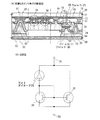
図1(A)は本発明の光センサチップの実装断面を示す図である。図1(A)では、2端子の可視光センサチップ(2.0mm×1.5mm)の例を示す。図1(A)において、10はガラス基板、12は下地絶縁膜、13はゲート絶縁膜である。受光する光はガラス基板10、下地絶縁膜12、およびゲート絶縁膜13を通過するため、これらの材料は全て透光性の高い材料を用いることが望ましい。
本実施の形態においては、実施の形態1の工程の一部をスクリーン印刷により行う例である。実施の形態1と同一の工程は簡略化のため、ここでは詳細な説明を省略することとする。
本実施の形態においては、レジスト形成をスクリーン印刷により行う例である。実施の形態1または実施の形態2と同一の工程は簡略化のため、ここでは詳細な説明を省略することとする。
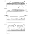
本実施の形態では、ガラス基板上に形成した光センサおよび増幅回路をガラス基板から剥離し、プラスチック基板に転写する作製方法を説明する。
本発明を実施して得た光センサチップを組み込むことによって様々な電子機器を作製することができる。電子機器としては、ビデオカメラ、デジタルカメラ、ゴーグル型ディスプレイ(ヘッドマウントディスプレイ)、プロジェクタ、液晶テレビなどのモニタ、ナビゲーションシステム、音響再生装置(カーオーディオ、オーディオコンポ等)、ノート型パーソナルコンピュータ、ゲーム機器、携帯情報端末(モバイルコンピュータ、携帯電話、携帯型ゲーム機または電子書籍等)、記録媒体を備えた画像再生装置(具体的にはDigital Versatile Disc(DVD)等の記録媒体を再生し、その画像を表示しうるディスプレイを備えた装置)などが挙げられる。
12:下地絶縁膜
13:ゲート絶縁膜
14:配線
15:配線
16:第2の層間絶縁膜
17:第3の層間絶縁膜
18:第1の電極
19:配線
20:接続電極
23:第2の電極
24:封止層
25:PIN型のフォトダイオード
26:端子電極
30:nチャネル型TFT
31:nチャネル型TFT
50:端子電極
51:端子電極
53:端子電極
60:プリント配線基板
61:電極
62:電極
63:半田
64:半田
Claims (14)
- 光センサー素子と増幅回路とを同一絶縁表面上に有し、
前記増幅回路は薄膜トランジスタで構成され、
前記光センサー素子は、前記薄膜トランジスタの配線上面及び側面を覆う第1の電極と、
前記配線及び前記第1の電極と重なるとともに、前記第1の電極上に一部接する光電変換層と、
前記光電変換層上に接する第2の電極と、を有していることを特徴とする半導体装置。 - 請求項1において、前記光センサー素子と前記増幅回路を有する前記半導体装置は、基板に固定されたチップであることを特徴とする半導体装置。
- 請求項2において、前記基板はガラス基板であることを特徴とする半導体装置。
- 請求項2において、前記基板はプラスチック基板であることを特徴とする半導体装置。
- 請求項2乃至請求項4のいずれか一において、前記チップに設けられた外部端子は2端子構成であることを特徴とする半導体装置。
- 請求項1乃至請求項5のいずれか一において、前記第1の電極は、Tiを含む膜であることを特徴とする半導体装置。
- 請求項1乃至請求項6のいずれか一において、前記薄膜トランジスタの前記配線は、Tiを含む第1の膜と、アルミニウムを含む膜と、Tiを含む第2の膜との三層構造を有することを特徴とする半導体装置。
- 請求項1乃至請求項7のいずれか一において、前記第2の電極は、前記光電変換層を介して前記第1の電極および前記配線と一部重なることを特徴とする半導体装置。
- 請求項1乃至請求項8のいずれか一において、前記半導体装置は、ビデオカメラ、デジタルカメラ、パーソナルコンピュータ、または携帯情報端末であることを特徴とする半導体装置。
- 光センサー素子と増幅回路とを同一絶縁表面上に有する半導体装置の作製方法であり、
増幅回路を構成する薄膜トランジスタの配線を形成する第1工程と、
前記配線の上面および側面を覆う第1の電極を形成する第2工程と、
前記配線および前記第1の電極と重なり、前記第1の電極上に一部接する光電変換層を形成する第3工程と、
前記光電変換層上に第2の電極を印刷法で形成する第4工程と、
前記第2の電極をマスクとして自己整合的に前記光電変換層をエッチングする第5工程と、を有することを特徴とする半導体装置の作製方法。 - 請求項10において、前記第5工程の後に、
前記第1の電極および前記第2の電極の端部を覆う封止層を印刷法で形成する第6工程と、
前記封止層上に前記第2の電極と接する第3の電極を印刷法で形成する第7の工程とを有することを特徴とする半導体装置の作製方法。 - 光センサー素子と増幅回路とを同一絶縁表面上に有する半導体装置の作製方法であり、
増幅回路を構成する薄膜トランジスタの配線を形成する第1工程と、
前記配線の上面および側面を覆う第1の電極を形成する第2工程と、
前記配線および前記第1の電極と重なり、前記第1の電極上に一部接する光電変換層を形成する第3工程と、
前記光電変換層上にレジストマスクを印刷法で形成する第4工程と、
前記レジストマスクをマスクとして前記光電変換層をエッチングする第5工程と、
前記レジストマスクを除去する第6工程と、
前記光電変換層上に第2の電極を印刷法で形成する第7工程と、を有することを特徴とする半導体装置の作製方法。 - 請求項12において、前記第7工程の後に、
前記第1の電極および前記第2の電極の端部を覆う封止層を印刷法で形成する第8工程と、
前記封止層上に前記第2の電極と接する第3の電極を印刷法で形成する第9の工程とを有することを特徴とする半導体装置の作製方法。 - 請求項10乃至請求項13のいずれか一において、前記第2の電極の形成は、前記光電変換層を介して前記配線および前記第1の電極と一部重なるように形成することを特徴とする半導体装置の作製方法。
Priority Applications (3)
| Application Number | Priority Date | Filing Date | Title |
|---|---|---|---|
| JP2004291554A JP4817636B2 (ja) | 2004-10-04 | 2004-10-04 | 半導体装置およびその作製方法 |
| US11/226,472 US7888714B2 (en) | 2004-10-04 | 2005-09-15 | Semiconductor device and method of manufacturing the same |
| CN200510108891A CN100585867C (zh) | 2004-10-04 | 2005-09-28 | 半导体装置及其制造方法 |
Applications Claiming Priority (1)
| Application Number | Priority Date | Filing Date | Title |
|---|---|---|---|
| JP2004291554A JP4817636B2 (ja) | 2004-10-04 | 2004-10-04 | 半導体装置およびその作製方法 |
Publications (3)
| Publication Number | Publication Date |
|---|---|
| JP2006108307A JP2006108307A (ja) | 2006-04-20 |
| JP2006108307A5 JP2006108307A5 (ja) | 2007-11-15 |
| JP4817636B2 true JP4817636B2 (ja) | 2011-11-16 |
Family
ID=36377689
Family Applications (1)
| Application Number | Title | Priority Date | Filing Date |
|---|---|---|---|
| JP2004291554A Expired - Fee Related JP4817636B2 (ja) | 2004-10-04 | 2004-10-04 | 半導体装置およびその作製方法 |
Country Status (3)
| Country | Link |
|---|---|
| US (1) | US7888714B2 (ja) |
| JP (1) | JP4817636B2 (ja) |
| CN (1) | CN100585867C (ja) |
Families Citing this family (20)
| Publication number | Priority date | Publication date | Assignee | Title |
|---|---|---|---|---|
| EP1724844A2 (en) * | 2005-05-20 | 2006-11-22 | Semiconductor Energy Laboratory Co., Ltd. | Photoelectric conversion device, manufacturing method thereof and semiconductor device |
| DE602007002105D1 (de) | 2006-04-28 | 2009-10-08 | Semiconductor Energy Lab | Halbleiterbauelement |
| KR101447044B1 (ko) * | 2006-10-31 | 2014-10-06 | 가부시키가이샤 한도오따이 에네루기 켄큐쇼 | 반도체장치 |
| JP5250236B2 (ja) * | 2006-10-31 | 2013-07-31 | 株式会社半導体エネルギー研究所 | 半導体装置及びその作製方法 |
| US8207589B2 (en) * | 2007-02-15 | 2012-06-26 | Semiconductor Energy Laboratory Co., Ltd. | Photoelectric conversion device and electronic device, and method for manufacturing photoelectric conversion device |
| WO2008123119A1 (en) * | 2007-03-26 | 2008-10-16 | Semiconductor Energy Laboratory Co., Ltd. | Photoelectric conversion device and electronic device provided with the photoelectric conversion device |
| KR101401528B1 (ko) * | 2007-06-29 | 2014-06-03 | 가부시키가이샤 한도오따이 에네루기 켄큐쇼 | 광전변환장치 및 그 광전변환장치를 구비하는 전자기기 |
| WO2009014155A1 (en) * | 2007-07-25 | 2009-01-29 | Semiconductor Energy Laboratory Co., Ltd. | Photoelectric conversion device and electronic device having the same |
| JP5317712B2 (ja) | 2008-01-22 | 2013-10-16 | 株式会社半導体エネルギー研究所 | 半導体装置及び半導体装置の作製方法 |
| JP5136112B2 (ja) * | 2008-02-19 | 2013-02-06 | セイコーエプソン株式会社 | 光電変換装置及び電気光学装置 |
| JP5388632B2 (ja) * | 2008-03-14 | 2014-01-15 | 株式会社半導体エネルギー研究所 | 半導体装置 |
| US9095066B2 (en) * | 2008-06-18 | 2015-07-28 | Semiconductor Energy Laboratory Co., Ltd. | Printed board |
| US8207487B2 (en) * | 2008-06-25 | 2012-06-26 | Semiconductor Energy Laboratory Co., Ltd. | Photoelectric conversion device including charge/discharge circuit |
| WO2010035608A1 (en) | 2008-09-25 | 2010-04-01 | Semiconductor Energy Laboratory Co., Ltd. | Semiconductor device and manufacturing method thereof |
| DE102010038933A1 (de) * | 2009-08-18 | 2011-02-24 | Denso Corporation, Kariya-City | Halbleitervorrichtung mit Halbleiterchip und Metallplatte und Verfahren zu deren Fertigung |
| US8946877B2 (en) * | 2010-09-29 | 2015-02-03 | Avago Technologies General Ip (Singapore) Pte. Ltd. | Semiconductor package including cap |
| US8580672B2 (en) | 2011-10-25 | 2013-11-12 | Globalfoundries Inc. | Methods of forming bump structures that include a protection layer |
| FR3006438B1 (fr) * | 2013-06-04 | 2015-06-26 | Commissariat Energie Atomique | Capteur de temperature |
| US9806217B2 (en) * | 2014-04-30 | 2017-10-31 | William Marsh Rice University | Fully integrated CMOS-compatible photodetector with color selectivity and intrinsic gain |
| CN105336751B (zh) * | 2014-06-23 | 2018-06-22 | 上海箩箕技术有限公司 | 光电传感器及其制造方法 |
Family Cites Families (67)
| Publication number | Priority date | Publication date | Assignee | Title |
|---|---|---|---|---|
| US4085411A (en) | 1976-04-16 | 1978-04-18 | Sprague Electric Company | Light detector system with photo diode and current-mirror amplifier |
| US4454416A (en) | 1982-01-13 | 1984-06-12 | Sprague Electric Company | Photo-electric circuit employing current mirrors |
| US4485301A (en) | 1982-02-01 | 1984-11-27 | Sprague Electric Company | Linear two-terminal integrated circuit photo sensor |
| EP0251563A3 (en) | 1986-06-17 | 1991-01-09 | Tokyo Electric Co. Ltd. | Photoelectric conversion device |
| JPH01289381A (ja) * | 1988-05-17 | 1989-11-21 | Seiko Epson Corp | 増幅型固体撮像装置 |
| CA2034118A1 (en) | 1990-02-09 | 1991-08-10 | Nang Tri Tran | Solid state radiation detector |
| JP3059514B2 (ja) | 1991-03-18 | 2000-07-04 | 株式会社半導体エネルギー研究所 | 光電変換装置ならびにイメージセンサおよびそれらの作製方法 |
| JP3255942B2 (ja) | 1991-06-19 | 2002-02-12 | 株式会社半導体エネルギー研究所 | 逆スタガ薄膜トランジスタの作製方法 |
| JPH0629510A (ja) * | 1991-10-16 | 1994-02-04 | Fuji Xerox Co Ltd | Tft駆動イメージセンサおよびその製造方法 |
| AU5306494A (en) | 1993-01-08 | 1994-07-14 | Richard A Vasichek | Magnetic keeper accessory for wrench sockets |
| JP3329512B2 (ja) | 1993-03-22 | 2002-09-30 | 株式会社半導体エネルギー研究所 | 半導体回路およびその作製方法 |
| US5501989A (en) | 1993-03-22 | 1996-03-26 | Semiconductor Energy Laboratory Co., Ltd. | Method of making semiconductor device/circuit having at least partially crystallized semiconductor layer |
| US7081938B1 (en) | 1993-12-03 | 2006-07-25 | Semiconductor Energy Laboratory Co., Ltd. | Electro-optical device and method for manufacturing the same |
| US6639262B2 (en) * | 1993-12-10 | 2003-10-28 | Symetrix Corporation | Metal oxide integrated circuit on silicon germanium substrate |
| JP3364081B2 (ja) | 1995-02-16 | 2003-01-08 | 株式会社半導体エネルギー研究所 | 半導体装置の作製方法 |
| US5757456A (en) | 1995-03-10 | 1998-05-26 | Semiconductor Energy Laboratory Co., Ltd. | Display device and method of fabricating involving peeling circuits from one substrate and mounting on other |
| US5834327A (en) | 1995-03-18 | 1998-11-10 | Semiconductor Energy Laboratory Co., Ltd. | Method for producing display device |
| JP3516424B2 (ja) | 1996-03-10 | 2004-04-05 | 株式会社半導体エネルギー研究所 | 薄膜半導体装置 |
| US5841180A (en) | 1996-03-27 | 1998-11-24 | Canon Kabushiki Kaisha | Photoelectric conversion device, method of driving photoelectric conversion device, and system having the device |
| JP3329680B2 (ja) | 1996-05-16 | 2002-09-30 | 株式会社デンソー | 光センサ |
| JP3444093B2 (ja) | 1996-06-10 | 2003-09-08 | 株式会社デンソー | 光センサ回路 |
| JP3719786B2 (ja) * | 1996-09-11 | 2005-11-24 | 株式会社東芝 | 光検出器の製造方法 |
| JP4027465B2 (ja) | 1997-07-01 | 2007-12-26 | 株式会社半導体エネルギー研究所 | アクティブマトリクス型表示装置およびその製造方法 |
| JP4127416B2 (ja) | 1997-07-16 | 2008-07-30 | 株式会社半導体エネルギー研究所 | 光センサ、光センサの作製方法、リニアイメージセンサ及びエリアセンサ |
| JP3838393B2 (ja) | 1997-09-02 | 2006-10-25 | 株式会社半導体エネルギー研究所 | イメージセンサを内蔵した表示装置 |
| JP4271268B2 (ja) | 1997-09-20 | 2009-06-03 | 株式会社半導体エネルギー研究所 | イメージセンサおよびイメージセンサ一体型アクティブマトリクス型表示装置 |
| JP4044187B2 (ja) | 1997-10-20 | 2008-02-06 | 株式会社半導体エネルギー研究所 | アクティブマトリクス型表示装置およびその作製方法 |
| US6287888B1 (en) | 1997-12-26 | 2001-09-11 | Semiconductor Energy Laboratory Co., Ltd. | Photoelectric conversion device and process for producing photoelectric conversion device |
| TW396707B (en) | 1998-02-20 | 2000-07-01 | Canon Kk | Semiconductor device |
| US6734907B1 (en) | 1998-04-30 | 2004-05-11 | Minolta Co., Ltd. | Solid-state image pickup device with integration and amplification |
| JPH11326954A (ja) | 1998-05-15 | 1999-11-26 | Semiconductor Energy Lab Co Ltd | 半導体装置 |
| US6867752B1 (en) | 1998-08-31 | 2005-03-15 | Semiconductor Energy Laboratory Co., Ltd. | Portable information processing system |
| JP3581031B2 (ja) | 1998-11-27 | 2004-10-27 | オリンパス株式会社 | 光検出装置 |
| US6858898B1 (en) | 1999-03-23 | 2005-02-22 | Semiconductor Energy Laboratory Co., Ltd. | Semiconductor device and method for manufacturing the same |
| TW480727B (en) | 2000-01-11 | 2002-03-21 | Semiconductor Energy Laboratro | Semiconductor display device |
| US6747638B2 (en) | 2000-01-31 | 2004-06-08 | Semiconductor Energy Laboratory Co., Ltd. | Adhesion type area sensor and display device having adhesion type area sensor |
| JP2001298663A (ja) | 2000-04-12 | 2001-10-26 | Semiconductor Energy Lab Co Ltd | 半導体装置およびその駆動方法 |
| JP4197217B2 (ja) | 2000-05-08 | 2008-12-17 | 株式会社半導体エネルギー研究所 | 装置 |
| JP4703815B2 (ja) | 2000-05-26 | 2011-06-15 | 株式会社半導体エネルギー研究所 | Mos型センサの駆動方法、及び撮像方法 |
| US6995753B2 (en) | 2000-06-06 | 2006-02-07 | Semiconductor Energy Laboratory Co., Ltd. | Display device and method of manufacturing the same |
| JP5110748B2 (ja) | 2000-06-06 | 2012-12-26 | 株式会社半導体エネルギー研究所 | 表示装置 |
| JP2002016839A (ja) | 2000-06-30 | 2002-01-18 | Minolta Co Ltd | 固体撮像装置 |
| JP2002176162A (ja) | 2000-08-10 | 2002-06-21 | Semiconductor Energy Lab Co Ltd | エリアセンサ及びエリアセンサを備えた表示装置 |
| US7030551B2 (en) | 2000-08-10 | 2006-04-18 | Semiconductor Energy Laboratory Co., Ltd. | Area sensor and display apparatus provided with an area sensor |
| US6724012B2 (en) | 2000-12-14 | 2004-04-20 | Semiconductor Energy Laboratory Co., Ltd. | Display matrix with pixels having sensor and light emitting portions |
| JP2002303676A (ja) | 2001-04-03 | 2002-10-18 | Matsushita Electric Ind Co Ltd | 放射線検出素子および放射線検出素子の製造方法 |
| JP4703883B2 (ja) | 2001-04-09 | 2011-06-15 | 株式会社半導体エネルギー研究所 | 半導体装置の作製方法 |
| JP4896302B2 (ja) | 2001-04-09 | 2012-03-14 | 株式会社半導体エネルギー研究所 | 半導体装置 |
| JP2002340989A (ja) | 2001-05-15 | 2002-11-27 | Semiconductor Energy Lab Co Ltd | 測定方法、検査方法及び検査装置 |
| JP2003047017A (ja) | 2001-07-10 | 2003-02-14 | Lg Electronics Inc | 3管式プロジェクションテレビの自動コンバーゼンス補正回路 |
| US8415208B2 (en) | 2001-07-16 | 2013-04-09 | Semiconductor Energy Laboratory Co., Ltd. | Semiconductor device and peeling off method and method of manufacturing semiconductor device |
| JP4027740B2 (ja) | 2001-07-16 | 2007-12-26 | 株式会社半導体エネルギー研究所 | 半導体装置の作製方法 |
| US6814832B2 (en) | 2001-07-24 | 2004-11-09 | Seiko Epson Corporation | Method for transferring element, method for producing element, integrated circuit, circuit board, electro-optical device, IC card, and electronic appliance |
| JP2003060744A (ja) | 2001-08-21 | 2003-02-28 | Sanyo Electric Co Ltd | 携帯機器 |
| US6956234B2 (en) | 2001-11-30 | 2005-10-18 | Semiconductor Energy Laboratory Co., Ltd. | Passive matrix display device |
| JP2003249671A (ja) | 2001-12-20 | 2003-09-05 | Canon Inc | 被覆樹脂層を有する基板の製造方法および製造装置 |
| TW575849B (en) | 2002-01-18 | 2004-02-11 | Chi Mei Optoelectronics Corp | Thin film transistor liquid crystal display capable of adjusting its light source |
| US6930326B2 (en) | 2002-03-26 | 2005-08-16 | Semiconductor Energy Laboratory Co., Ltd. | Semiconductor circuit and method of fabricating the same |
| DE60325669D1 (de) | 2002-05-17 | 2009-02-26 | Semiconductor Energy Lab | Verfahren zum Transferieren eines Objekts und Verfahren zur Herstellung eines Halbleiterbauelements |
| JP2004015000A (ja) * | 2002-06-11 | 2004-01-15 | Canon Inc | 放射線検出装置及び放射線撮像システム |
| US7078702B2 (en) * | 2002-07-25 | 2006-07-18 | General Electric Company | Imager |
| JP2004140267A (ja) | 2002-10-18 | 2004-05-13 | Semiconductor Energy Lab Co Ltd | 半導体装置およびその作製方法 |
| KR101032337B1 (ko) | 2002-12-13 | 2011-05-09 | 가부시키가이샤 한도오따이 에네루기 켄큐쇼 | 발광장치 및 그의 제조방법 |
| EP1583148A4 (en) | 2003-01-08 | 2007-06-27 | Semiconductor Energy Lab | SEMICONDUCTOR DEVICE AND METHOD FOR PRODUCING THE SAME |
| US6982406B2 (en) | 2003-04-03 | 2006-01-03 | Pao Jung Chen | Simple CMOS light-to-current sensor |
| US7253391B2 (en) | 2003-09-19 | 2007-08-07 | Semiconductor Energy Laboratory Co., Ltd. | Optical sensor device and electronic apparatus |
| CN100477240C (zh) | 2003-10-06 | 2009-04-08 | 株式会社半导体能源研究所 | 半导体器件以及制造该器件的方法 |
-
2004
- 2004-10-04 JP JP2004291554A patent/JP4817636B2/ja not_active Expired - Fee Related
-
2005
- 2005-09-15 US US11/226,472 patent/US7888714B2/en not_active Expired - Fee Related
- 2005-09-28 CN CN200510108891A patent/CN100585867C/zh not_active Expired - Fee Related
Also Published As
| Publication number | Publication date |
|---|---|
| JP2006108307A (ja) | 2006-04-20 |
| US20070187790A1 (en) | 2007-08-16 |
| CN100585867C (zh) | 2010-01-27 |
| CN1783506A (zh) | 2006-06-07 |
| US7888714B2 (en) | 2011-02-15 |
Similar Documents
| Publication | Publication Date | Title |
|---|---|---|
| US7888714B2 (en) | Semiconductor device and method of manufacturing the same | |
| KR101273971B1 (ko) | 반도체장치 및 그 제조방법 | |
| JP5784096B2 (ja) | 半導体装置の作製方法 | |
| KR101227022B1 (ko) | 광전 변환 장치 및 그 제작 방법과, 반도체 장치 | |
| JP5277263B2 (ja) | 発光装置の作製方法 | |
| US8207591B2 (en) | Photoelectric conversion device | |
| US7923800B2 (en) | Semiconductor device and electronic device | |
| JP4827396B2 (ja) | 半導体装置の作製方法 | |
| JP5844858B2 (ja) | 半導体装置の作製方法、及び、半導体装置 | |
| JP4809715B2 (ja) | 光電変換装置及びその作製方法、並びに半導体装置 | |
| JP2006013462A (ja) | 半導体装置及びその作製方法 | |
| JP4532418B2 (ja) | 光センサ及びその作製方法 | |
| JP4267394B2 (ja) | 剥離方法、及び半導体装置の作製方法 |
Legal Events
| Date | Code | Title | Description |
|---|---|---|---|
| A521 | Request for written amendment filed |
Free format text: JAPANESE INTERMEDIATE CODE: A523 Effective date: 20071002 |
|
| A621 | Written request for application examination |
Free format text: JAPANESE INTERMEDIATE CODE: A621 Effective date: 20071002 |
|
| A977 | Report on retrieval |
Free format text: JAPANESE INTERMEDIATE CODE: A971007 Effective date: 20100826 |
|
| TRDD | Decision of grant or rejection written | ||
| A01 | Written decision to grant a patent or to grant a registration (utility model) |
Free format text: JAPANESE INTERMEDIATE CODE: A01 Effective date: 20110823 |
|
| A01 | Written decision to grant a patent or to grant a registration (utility model) |
Free format text: JAPANESE INTERMEDIATE CODE: A01 |
|
| A61 | First payment of annual fees (during grant procedure) |
Free format text: JAPANESE INTERMEDIATE CODE: A61 Effective date: 20110830 |
|
| FPAY | Renewal fee payment (event date is renewal date of database) |
Free format text: PAYMENT UNTIL: 20140909 Year of fee payment: 3 |
|
| R150 | Certificate of patent or registration of utility model |
Ref document number: 4817636 Country of ref document: JP Free format text: JAPANESE INTERMEDIATE CODE: R150 Free format text: JAPANESE INTERMEDIATE CODE: R150 |
|
| FPAY | Renewal fee payment (event date is renewal date of database) |
Free format text: PAYMENT UNTIL: 20140909 Year of fee payment: 3 |
|
| R250 | Receipt of annual fees |
Free format text: JAPANESE INTERMEDIATE CODE: R250 |
|
| R250 | Receipt of annual fees |
Free format text: JAPANESE INTERMEDIATE CODE: R250 |
|
| R250 | Receipt of annual fees |
Free format text: JAPANESE INTERMEDIATE CODE: R250 |
|
| R250 | Receipt of annual fees |
Free format text: JAPANESE INTERMEDIATE CODE: R250 |
|
| R250 | Receipt of annual fees |
Free format text: JAPANESE INTERMEDIATE CODE: R250 |
|
| R250 | Receipt of annual fees |
Free format text: JAPANESE INTERMEDIATE CODE: R250 |
|
| LAPS | Cancellation because of no payment of annual fees |