JP4711446B2 - Finfetと一体化した平坦基板デバイス及びその製造方法 - Google Patents
Finfetと一体化した平坦基板デバイス及びその製造方法 Download PDFInfo
- Publication number
- JP4711446B2 JP4711446B2 JP2007536791A JP2007536791A JP4711446B2 JP 4711446 B2 JP4711446 B2 JP 4711446B2 JP 2007536791 A JP2007536791 A JP 2007536791A JP 2007536791 A JP2007536791 A JP 2007536791A JP 4711446 B2 JP4711446 B2 JP 4711446B2
- Authority
- JP
- Japan
- Prior art keywords
- substrate
- finfet
- fet
- layer
- gate
- Prior art date
- Legal status (The legal status is an assumption and is not a legal conclusion. Google has not performed a legal analysis and makes no representation as to the accuracy of the status listed.)
- Expired - Fee Related
Links
- 239000000758 substrate Substances 0.000 title claims description 66
- 238000004519 manufacturing process Methods 0.000 title description 23
- 238000002955 isolation Methods 0.000 claims description 44
- 238000000034 method Methods 0.000 claims description 33
- 239000004065 semiconductor Substances 0.000 claims description 22
- 239000000463 material Substances 0.000 claims description 20
- 238000005530 etching Methods 0.000 claims description 11
- 230000005669 field effect Effects 0.000 claims description 11
- 238000000151 deposition Methods 0.000 claims description 5
- 239000012212 insulator Substances 0.000 claims description 4
- 230000008878 coupling Effects 0.000 claims description 2
- 238000010168 coupling process Methods 0.000 claims description 2
- 238000005859 coupling reaction Methods 0.000 claims description 2
- 238000012545 processing Methods 0.000 description 13
- XUIMIQQOPSSXEZ-UHFFFAOYSA-N Silicon Chemical compound [Si] XUIMIQQOPSSXEZ-UHFFFAOYSA-N 0.000 description 10
- 229910052710 silicon Inorganic materials 0.000 description 10
- 239000010703 silicon Substances 0.000 description 10
- 230000015572 biosynthetic process Effects 0.000 description 8
- 239000007943 implant Substances 0.000 description 6
- 230000008569 process Effects 0.000 description 6
- 238000012986 modification Methods 0.000 description 5
- 230000004048 modification Effects 0.000 description 5
- 230000008021 deposition Effects 0.000 description 4
- 229910021420 polycrystalline silicon Inorganic materials 0.000 description 4
- 229920005591 polysilicon Polymers 0.000 description 4
- 229910000577 Silicon-germanium Inorganic materials 0.000 description 3
- 230000008901 benefit Effects 0.000 description 3
- 238000010586 diagram Methods 0.000 description 3
- 125000001475 halogen functional group Chemical group 0.000 description 3
- ZOXJGFHDIHLPTG-UHFFFAOYSA-N Boron Chemical compound [B] ZOXJGFHDIHLPTG-UHFFFAOYSA-N 0.000 description 2
- GYHNNYVSQQEPJS-UHFFFAOYSA-N Gallium Chemical compound [Ga] GYHNNYVSQQEPJS-UHFFFAOYSA-N 0.000 description 2
- LEVVHYCKPQWKOP-UHFFFAOYSA-N [Si].[Ge] Chemical compound [Si].[Ge] LEVVHYCKPQWKOP-UHFFFAOYSA-N 0.000 description 2
- 229910052787 antimony Inorganic materials 0.000 description 2
- WATWJIUSRGPENY-UHFFFAOYSA-N antimony atom Chemical compound [Sb] WATWJIUSRGPENY-UHFFFAOYSA-N 0.000 description 2
- 229910052785 arsenic Inorganic materials 0.000 description 2
- RQNWIZPPADIBDY-UHFFFAOYSA-N arsenic atom Chemical compound [As] RQNWIZPPADIBDY-UHFFFAOYSA-N 0.000 description 2
- 229910052796 boron Inorganic materials 0.000 description 2
- 238000001311 chemical methods and process Methods 0.000 description 2
- 238000013461 design Methods 0.000 description 2
- 238000005516 engineering process Methods 0.000 description 2
- 230000006870 function Effects 0.000 description 2
- 229910052733 gallium Inorganic materials 0.000 description 2
- BHEPBYXIRTUNPN-UHFFFAOYSA-N hydridophosphorus(.) (triplet) Chemical compound [PH] BHEPBYXIRTUNPN-UHFFFAOYSA-N 0.000 description 2
- 238000002513 implantation Methods 0.000 description 2
- 229910052738 indium Inorganic materials 0.000 description 2
- APFVFJFRJDLVQX-UHFFFAOYSA-N indium atom Chemical compound [In] APFVFJFRJDLVQX-UHFFFAOYSA-N 0.000 description 2
- 230000010354 integration Effects 0.000 description 2
- 238000005468 ion implantation Methods 0.000 description 2
- 238000001459 lithography Methods 0.000 description 2
- 238000001020 plasma etching Methods 0.000 description 2
- 230000009467 reduction Effects 0.000 description 2
- 238000000926 separation method Methods 0.000 description 2
- JBRZTFJDHDCESZ-UHFFFAOYSA-N AsGa Chemical compound [As]#[Ga] JBRZTFJDHDCESZ-UHFFFAOYSA-N 0.000 description 1
- GPXJNWSHGFTCBW-UHFFFAOYSA-N Indium phosphide Chemical compound [In]#P GPXJNWSHGFTCBW-UHFFFAOYSA-N 0.000 description 1
- 230000006978 adaptation Effects 0.000 description 1
- 238000000137 annealing Methods 0.000 description 1
- 238000013459 approach Methods 0.000 description 1
- 239000003990 capacitor Substances 0.000 description 1
- 230000000295 complement effect Effects 0.000 description 1
- 150000001875 compounds Chemical class 0.000 description 1
- 238000007796 conventional method Methods 0.000 description 1
- 230000003247 decreasing effect Effects 0.000 description 1
- 230000000694 effects Effects 0.000 description 1
- 238000011049 filling Methods 0.000 description 1
- HZXMRANICFIONG-UHFFFAOYSA-N gallium phosphide Chemical compound [Ga]#P HZXMRANICFIONG-UHFFFAOYSA-N 0.000 description 1
- 238000007429 general method Methods 0.000 description 1
- 229910052732 germanium Inorganic materials 0.000 description 1
- GNPVGFCGXDBREM-UHFFFAOYSA-N germanium atom Chemical compound [Ge] GNPVGFCGXDBREM-UHFFFAOYSA-N 0.000 description 1
- RPQDHPTXJYYUPQ-UHFFFAOYSA-N indium arsenide Chemical compound [In]#[As] RPQDHPTXJYYUPQ-UHFFFAOYSA-N 0.000 description 1
- 238000002347 injection Methods 0.000 description 1
- 239000007924 injection Substances 0.000 description 1
- 239000011810 insulating material Substances 0.000 description 1
- 229910044991 metal oxide Inorganic materials 0.000 description 1
- 150000004706 metal oxides Chemical class 0.000 description 1
- 238000004377 microelectronic Methods 0.000 description 1
- 229910021421 monocrystalline silicon Inorganic materials 0.000 description 1
- 150000004767 nitrides Chemical class 0.000 description 1
- 230000003647 oxidation Effects 0.000 description 1
- 238000007254 oxidation reaction Methods 0.000 description 1
- 238000007517 polishing process Methods 0.000 description 1
- 239000000126 substance Substances 0.000 description 1
Images


Classifications
-
- H—ELECTRICITY
- H01—ELECTRIC ELEMENTS
- H01L—SEMICONDUCTOR DEVICES NOT COVERED BY CLASS H10
- H01L27/00—Devices consisting of a plurality of semiconductor or other solid-state components formed in or on a common substrate
- H01L27/02—Devices consisting of a plurality of semiconductor or other solid-state components formed in or on a common substrate including semiconductor components specially adapted for rectifying, oscillating, amplifying or switching and having at least one potential-jump barrier or surface barrier; including integrated passive circuit elements with at least one potential-jump barrier or surface barrier
- H01L27/12—Devices consisting of a plurality of semiconductor or other solid-state components formed in or on a common substrate including semiconductor components specially adapted for rectifying, oscillating, amplifying or switching and having at least one potential-jump barrier or surface barrier; including integrated passive circuit elements with at least one potential-jump barrier or surface barrier the substrate being other than a semiconductor body, e.g. an insulating body
- H01L27/1203—Devices consisting of a plurality of semiconductor or other solid-state components formed in or on a common substrate including semiconductor components specially adapted for rectifying, oscillating, amplifying or switching and having at least one potential-jump barrier or surface barrier; including integrated passive circuit elements with at least one potential-jump barrier or surface barrier the substrate being other than a semiconductor body, e.g. an insulating body the substrate comprising an insulating body on a semiconductor body, e.g. SOI
- H01L27/1211—Devices consisting of a plurality of semiconductor or other solid-state components formed in or on a common substrate including semiconductor components specially adapted for rectifying, oscillating, amplifying or switching and having at least one potential-jump barrier or surface barrier; including integrated passive circuit elements with at least one potential-jump barrier or surface barrier the substrate being other than a semiconductor body, e.g. an insulating body the substrate comprising an insulating body on a semiconductor body, e.g. SOI combined with field-effect transistors with a horizontal current flow in a vertical sidewall of a semiconductor body, e.g. FinFET, MuGFET
-
- H—ELECTRICITY
- H01—ELECTRIC ELEMENTS
- H01L—SEMICONDUCTOR DEVICES NOT COVERED BY CLASS H10
- H01L29/00—Semiconductor devices adapted for rectifying, amplifying, oscillating or switching, or capacitors or resistors with at least one potential-jump barrier or surface barrier, e.g. PN junction depletion layer or carrier concentration layer; Details of semiconductor bodies or of electrodes thereof ; Multistep manufacturing processes therefor
- H01L29/66—Types of semiconductor device ; Multistep manufacturing processes therefor
- H01L29/68—Types of semiconductor device ; Multistep manufacturing processes therefor controllable by only the electric current supplied, or only the electric potential applied, to an electrode which does not carry the current to be rectified, amplified or switched
- H01L29/76—Unipolar devices, e.g. field effect transistors
- H01L29/772—Field effect transistors
- H01L29/78—Field effect transistors with field effect produced by an insulated gate
- H01L29/785—Field effect transistors with field effect produced by an insulated gate having a channel with a horizontal current flow in a vertical sidewall of a semiconductor body, e.g. FinFET, MuGFET
-
- H—ELECTRICITY
- H01—ELECTRIC ELEMENTS
- H01L—SEMICONDUCTOR DEVICES NOT COVERED BY CLASS H10
- H01L21/00—Processes or apparatus adapted for the manufacture or treatment of semiconductor or solid state devices or of parts thereof
- H01L21/70—Manufacture or treatment of devices consisting of a plurality of solid state components formed in or on a common substrate or of parts thereof; Manufacture of integrated circuit devices or of parts thereof
- H01L21/77—Manufacture or treatment of devices consisting of a plurality of solid state components or integrated circuits formed in, or on, a common substrate
- H01L21/78—Manufacture or treatment of devices consisting of a plurality of solid state components or integrated circuits formed in, or on, a common substrate with subsequent division of the substrate into plural individual devices
- H01L21/82—Manufacture or treatment of devices consisting of a plurality of solid state components or integrated circuits formed in, or on, a common substrate with subsequent division of the substrate into plural individual devices to produce devices, e.g. integrated circuits, each consisting of a plurality of components
- H01L21/822—Manufacture or treatment of devices consisting of a plurality of solid state components or integrated circuits formed in, or on, a common substrate with subsequent division of the substrate into plural individual devices to produce devices, e.g. integrated circuits, each consisting of a plurality of components the substrate being a semiconductor, using silicon technology
- H01L21/8232—Field-effect technology
- H01L21/8234—MIS technology, i.e. integration processes of field effect transistors of the conductor-insulator-semiconductor type
- H01L21/8238—Complementary field-effect transistors, e.g. CMOS
- H01L21/823821—Complementary field-effect transistors, e.g. CMOS with a particular manufacturing method of transistors with a horizontal current flow in a vertical sidewall of a semiconductor body, e.g. FinFET, MuGFET
-
- H—ELECTRICITY
- H01—ELECTRIC ELEMENTS
- H01L—SEMICONDUCTOR DEVICES NOT COVERED BY CLASS H10
- H01L21/00—Processes or apparatus adapted for the manufacture or treatment of semiconductor or solid state devices or of parts thereof
- H01L21/70—Manufacture or treatment of devices consisting of a plurality of solid state components formed in or on a common substrate or of parts thereof; Manufacture of integrated circuit devices or of parts thereof
- H01L21/77—Manufacture or treatment of devices consisting of a plurality of solid state components or integrated circuits formed in, or on, a common substrate
- H01L21/78—Manufacture or treatment of devices consisting of a plurality of solid state components or integrated circuits formed in, or on, a common substrate with subsequent division of the substrate into plural individual devices
- H01L21/82—Manufacture or treatment of devices consisting of a plurality of solid state components or integrated circuits formed in, or on, a common substrate with subsequent division of the substrate into plural individual devices to produce devices, e.g. integrated circuits, each consisting of a plurality of components
- H01L21/822—Manufacture or treatment of devices consisting of a plurality of solid state components or integrated circuits formed in, or on, a common substrate with subsequent division of the substrate into plural individual devices to produce devices, e.g. integrated circuits, each consisting of a plurality of components the substrate being a semiconductor, using silicon technology
- H01L21/8232—Field-effect technology
- H01L21/8234—MIS technology, i.e. integration processes of field effect transistors of the conductor-insulator-semiconductor type
- H01L21/8238—Complementary field-effect transistors, e.g. CMOS
- H01L21/823828—Complementary field-effect transistors, e.g. CMOS with a particular manufacturing method of the gate conductors, e.g. particular materials, shapes
-
- H—ELECTRICITY
- H01—ELECTRIC ELEMENTS
- H01L—SEMICONDUCTOR DEVICES NOT COVERED BY CLASS H10
- H01L21/00—Processes or apparatus adapted for the manufacture or treatment of semiconductor or solid state devices or of parts thereof
- H01L21/70—Manufacture or treatment of devices consisting of a plurality of solid state components formed in or on a common substrate or of parts thereof; Manufacture of integrated circuit devices or of parts thereof
- H01L21/77—Manufacture or treatment of devices consisting of a plurality of solid state components or integrated circuits formed in, or on, a common substrate
- H01L21/78—Manufacture or treatment of devices consisting of a plurality of solid state components or integrated circuits formed in, or on, a common substrate with subsequent division of the substrate into plural individual devices
- H01L21/82—Manufacture or treatment of devices consisting of a plurality of solid state components or integrated circuits formed in, or on, a common substrate with subsequent division of the substrate into plural individual devices to produce devices, e.g. integrated circuits, each consisting of a plurality of components
- H01L21/822—Manufacture or treatment of devices consisting of a plurality of solid state components or integrated circuits formed in, or on, a common substrate with subsequent division of the substrate into plural individual devices to produce devices, e.g. integrated circuits, each consisting of a plurality of components the substrate being a semiconductor, using silicon technology
- H01L21/8232—Field-effect technology
- H01L21/8234—MIS technology, i.e. integration processes of field effect transistors of the conductor-insulator-semiconductor type
- H01L21/8238—Complementary field-effect transistors, e.g. CMOS
- H01L21/823878—Complementary field-effect transistors, e.g. CMOS isolation region manufacturing related aspects, e.g. to avoid interaction of isolation region with adjacent structure
-
- H—ELECTRICITY
- H01—ELECTRIC ELEMENTS
- H01L—SEMICONDUCTOR DEVICES NOT COVERED BY CLASS H10
- H01L21/00—Processes or apparatus adapted for the manufacture or treatment of semiconductor or solid state devices or of parts thereof
- H01L21/70—Manufacture or treatment of devices consisting of a plurality of solid state components formed in or on a common substrate or of parts thereof; Manufacture of integrated circuit devices or of parts thereof
- H01L21/77—Manufacture or treatment of devices consisting of a plurality of solid state components or integrated circuits formed in, or on, a common substrate
- H01L21/78—Manufacture or treatment of devices consisting of a plurality of solid state components or integrated circuits formed in, or on, a common substrate with subsequent division of the substrate into plural individual devices
- H01L21/82—Manufacture or treatment of devices consisting of a plurality of solid state components or integrated circuits formed in, or on, a common substrate with subsequent division of the substrate into plural individual devices to produce devices, e.g. integrated circuits, each consisting of a plurality of components
- H01L21/84—Manufacture or treatment of devices consisting of a plurality of solid state components or integrated circuits formed in, or on, a common substrate with subsequent division of the substrate into plural individual devices to produce devices, e.g. integrated circuits, each consisting of a plurality of components the substrate being other than a semiconductor body, e.g. being an insulating body
- H01L21/845—Manufacture or treatment of devices consisting of a plurality of solid state components or integrated circuits formed in, or on, a common substrate with subsequent division of the substrate into plural individual devices to produce devices, e.g. integrated circuits, each consisting of a plurality of components the substrate being other than a semiconductor body, e.g. being an insulating body including field-effect transistors with a horizontal current flow in a vertical sidewall of a semiconductor body, e.g. FinFET, MuGFET
-
- H—ELECTRICITY
- H01—ELECTRIC ELEMENTS
- H01L—SEMICONDUCTOR DEVICES NOT COVERED BY CLASS H10
- H01L27/00—Devices consisting of a plurality of semiconductor or other solid-state components formed in or on a common substrate
- H01L27/02—Devices consisting of a plurality of semiconductor or other solid-state components formed in or on a common substrate including semiconductor components specially adapted for rectifying, oscillating, amplifying or switching and having at least one potential-jump barrier or surface barrier; including integrated passive circuit elements with at least one potential-jump barrier or surface barrier
- H01L27/04—Devices consisting of a plurality of semiconductor or other solid-state components formed in or on a common substrate including semiconductor components specially adapted for rectifying, oscillating, amplifying or switching and having at least one potential-jump barrier or surface barrier; including integrated passive circuit elements with at least one potential-jump barrier or surface barrier the substrate being a semiconductor body
- H01L27/08—Devices consisting of a plurality of semiconductor or other solid-state components formed in or on a common substrate including semiconductor components specially adapted for rectifying, oscillating, amplifying or switching and having at least one potential-jump barrier or surface barrier; including integrated passive circuit elements with at least one potential-jump barrier or surface barrier the substrate being a semiconductor body including only semiconductor components of a single kind
- H01L27/085—Devices consisting of a plurality of semiconductor or other solid-state components formed in or on a common substrate including semiconductor components specially adapted for rectifying, oscillating, amplifying or switching and having at least one potential-jump barrier or surface barrier; including integrated passive circuit elements with at least one potential-jump barrier or surface barrier the substrate being a semiconductor body including only semiconductor components of a single kind including field-effect components only
- H01L27/088—Devices consisting of a plurality of semiconductor or other solid-state components formed in or on a common substrate including semiconductor components specially adapted for rectifying, oscillating, amplifying or switching and having at least one potential-jump barrier or surface barrier; including integrated passive circuit elements with at least one potential-jump barrier or surface barrier the substrate being a semiconductor body including only semiconductor components of a single kind including field-effect components only the components being field-effect transistors with insulated gate
- H01L27/092—Devices consisting of a plurality of semiconductor or other solid-state components formed in or on a common substrate including semiconductor components specially adapted for rectifying, oscillating, amplifying or switching and having at least one potential-jump barrier or surface barrier; including integrated passive circuit elements with at least one potential-jump barrier or surface barrier the substrate being a semiconductor body including only semiconductor components of a single kind including field-effect components only the components being field-effect transistors with insulated gate complementary MIS field-effect transistors
- H01L27/0924—Devices consisting of a plurality of semiconductor or other solid-state components formed in or on a common substrate including semiconductor components specially adapted for rectifying, oscillating, amplifying or switching and having at least one potential-jump barrier or surface barrier; including integrated passive circuit elements with at least one potential-jump barrier or surface barrier the substrate being a semiconductor body including only semiconductor components of a single kind including field-effect components only the components being field-effect transistors with insulated gate complementary MIS field-effect transistors including transistors with a horizontal current flow in a vertical sidewall of a semiconductor body, e.g. FinFET, MuGFET
-
- H—ELECTRICITY
- H01—ELECTRIC ELEMENTS
- H01L—SEMICONDUCTOR DEVICES NOT COVERED BY CLASS H10
- H01L29/00—Semiconductor devices adapted for rectifying, amplifying, oscillating or switching, or capacitors or resistors with at least one potential-jump barrier or surface barrier, e.g. PN junction depletion layer or carrier concentration layer; Details of semiconductor bodies or of electrodes thereof ; Multistep manufacturing processes therefor
- H01L29/66—Types of semiconductor device ; Multistep manufacturing processes therefor
- H01L29/66007—Multistep manufacturing processes
- H01L29/66075—Multistep manufacturing processes of devices having semiconductor bodies comprising group 14 or group 13/15 materials
- H01L29/66227—Multistep manufacturing processes of devices having semiconductor bodies comprising group 14 or group 13/15 materials the devices being controllable only by the electric current supplied or the electric potential applied, to an electrode which does not carry the current to be rectified, amplified or switched, e.g. three-terminal devices
- H01L29/66409—Unipolar field-effect transistors
- H01L29/66477—Unipolar field-effect transistors with an insulated gate, i.e. MISFET
- H01L29/66787—Unipolar field-effect transistors with an insulated gate, i.e. MISFET with a gate at the side of the channel
- H01L29/66795—Unipolar field-effect transistors with an insulated gate, i.e. MISFET with a gate at the side of the channel with a horizontal current flow in a vertical sidewall of a semiconductor body, e.g. FinFET, MuGFET
Description
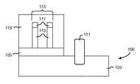
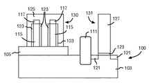
101:SOIウエハ
102:デバイス
103:基板
104、106、108、110:逆型ウェル領域
105:埋め込み分離層
111:浅いトレンチ分離領域
115:シリコン層
125:FinFETゲート
127:FETゲート
130:FinFET
131:平坦型FET
Claims (3)
- 基板と、
前記基板上の埋め込み分離層と、
前記埋め込み分離層上のフィン型電解効果トランジスタ(FinFET)と、
前記基板における平坦型電解効果トランジスタ(FET)であって、前記FETのゲート領域が前記FinFETのゲート領域と同様な高さに形成される、平坦型電解効果トランジスタ(FET)と、
を含む構造体。 - 基板と、
前記基板上の埋め込み分離層と、
前記埋め込み分離層上の半導体層と、
を含むシリコン・オン・インシュレータ(SOI)ウエハと、
前記埋め込み分離層上のフィン型電解効果トランジスタ(FinFET)と、
前記基板に組み込まれた平坦型電解効果トランジスタ(FET)であって、前記FETのゲート領域が前記FinFETのゲート領域と同様な高さに形成される、平坦型電解効果トランジスタ(FET)と、
を含む構造体。 - フィン型電解効果トランジスタ(FinFET)と一体化した平坦型電界効果トランジスタ(FET)基板デバイスを形成するための方法であって、
基板を準備するステップと、
埋め込み分離層を前記基板上に形成するステップと、
半導体層を前記埋め込み分離層に結合するステップと、
第1の誘電体層を前記半導体層上に形成した後、該第1の誘電体層をハードマスクとして該半導体層をエッチングしてフィン型構造体を形成するステップと、
前記埋め込み分離層の一部分を選択的に除去して前記基板を露出させるステップと、
前記フィン型構造体の側壁の上及び露出した前記基板の上に第2の誘電体層を形成するステップと、
前記第1の誘電体層の上及び前記第2の誘電体層の上にゲート材料を同時に堆積するステップと、
前記ゲート材料を同時に平坦化してFinFETのゲート領域とFETのゲート領域とを同様な高さに形成するステップと、
含む方法。
Applications Claiming Priority (3)
| Application Number | Priority Date | Filing Date | Title |
|---|---|---|---|
| US10/711,974 | 2004-10-18 | ||
| US10/711,974 US6949768B1 (en) | 2004-10-18 | 2004-10-18 | Planar substrate devices integrated with finfets and method of manufacture |
| PCT/US2005/036471 WO2006044349A2 (en) | 2004-10-18 | 2005-10-11 | Planar substrate devices integrated with finfets and method of manufacture |
Publications (3)
| Publication Number | Publication Date |
|---|---|
| JP2008517464A JP2008517464A (ja) | 2008-05-22 |
| JP2008517464A5 JP2008517464A5 (ja) | 2008-09-04 |
| JP4711446B2 true JP4711446B2 (ja) | 2011-06-29 |
Family
ID=34992630
Family Applications (1)
| Application Number | Title | Priority Date | Filing Date |
|---|---|---|---|
| JP2007536791A Expired - Fee Related JP4711446B2 (ja) | 2004-10-18 | 2005-10-11 | Finfetと一体化した平坦基板デバイス及びその製造方法 |
Country Status (7)
| Country | Link |
|---|---|
| US (2) | US6949768B1 (ja) |
| EP (1) | EP1805795A4 (ja) |
| JP (1) | JP4711446B2 (ja) |
| KR (2) | KR100985639B1 (ja) |
| CN (1) | CN100533758C (ja) |
| TW (1) | TWI380343B (ja) |
| WO (1) | WO2006044349A2 (ja) |
Families Citing this family (98)
| Publication number | Priority date | Publication date | Assignee | Title |
|---|---|---|---|---|
| WO2006006438A1 (ja) * | 2004-07-12 | 2006-01-19 | Nec Corporation | 半導体装置及びその製造方法 |
| JP2006049627A (ja) * | 2004-08-05 | 2006-02-16 | Toshiba Corp | 半導体装置及びその製造方法 |
| KR100612419B1 (ko) * | 2004-10-19 | 2006-08-16 | 삼성전자주식회사 | 핀 트랜지스터 및 평판 트랜지스터를 갖는 반도체 소자 및그 형성 방법 |
| JP2006261188A (ja) * | 2005-03-15 | 2006-09-28 | Seiko Epson Corp | 半導体装置の製造方法及び半導体装置 |
| US7920544B2 (en) * | 2005-03-28 | 2011-04-05 | Qualcomm Incorporated | Method and apparatus for enhancing signal-to-noise ratio of position location measurements |
| JP2007018588A (ja) * | 2005-07-06 | 2007-01-25 | Toshiba Corp | 半導体記憶装置および半導体記憶装置の駆動方法 |
| WO2007049170A1 (en) * | 2005-10-25 | 2007-05-03 | Nxp B.V. | Finfet transistors |
| US7512017B2 (en) * | 2005-12-21 | 2009-03-31 | Intel Corporation | Integration of planar and tri-gate devices on the same substrate |
| US7264743B2 (en) * | 2006-01-23 | 2007-09-04 | Lam Research Corporation | Fin structure formation |
| JP2007294857A (ja) * | 2006-03-28 | 2007-11-08 | Elpida Memory Inc | 半導体装置及びその製造方法 |
| US7803670B2 (en) * | 2006-07-20 | 2010-09-28 | Freescale Semiconductor, Inc. | Twisted dual-substrate orientation (DSO) substrates |
| US7456471B2 (en) * | 2006-09-15 | 2008-11-25 | International Business Machines Corporation | Field effect transistor with raised source/drain fin straps |
| US8368144B2 (en) * | 2006-12-18 | 2013-02-05 | Infineon Technologies Ag | Isolated multigate FET circuit blocks with different ground potentials |
| US8492796B2 (en) * | 2007-03-13 | 2013-07-23 | Infineon Technologies Ag | MuGFET switch |
| US7923337B2 (en) * | 2007-06-20 | 2011-04-12 | International Business Machines Corporation | Fin field effect transistor devices with self-aligned source and drain regions |
| JP4459257B2 (ja) * | 2007-06-27 | 2010-04-28 | 株式会社東芝 | 半導体装置 |
| US9064963B2 (en) * | 2007-09-28 | 2015-06-23 | Infineon Technologies Ag | Semiconductor structure |
| US8329564B2 (en) * | 2007-10-26 | 2012-12-11 | International Business Machines Corporation | Method for fabricating super-steep retrograde well MOSFET on SOI or bulk silicon substrate, and device fabricated in accordance with the method |
| US7786535B2 (en) * | 2008-01-11 | 2010-08-31 | International Business Machines Corporation | Design structures for high-voltage integrated circuits |
| US7790543B2 (en) * | 2008-01-11 | 2010-09-07 | International Business Machines Corporation | Device structures for a metal-oxide-semiconductor field effect transistor and methods of fabricating such device structures |
| US7790524B2 (en) * | 2008-01-11 | 2010-09-07 | International Business Machines Corporation | Device and design structures for memory cells in a non-volatile random access memory and methods of fabricating such device structures |
| US7772651B2 (en) * | 2008-01-11 | 2010-08-10 | International Business Machines Corporation | Semiconductor-on-insulator high-voltage device structures, methods of fabricating such device structures, and design structures for high-voltage circuits |
| WO2009110048A1 (ja) * | 2008-02-15 | 2009-09-11 | 日本ユニサンティスエレクトロニクス株式会社 | 半導体装置及びその製造方法 |
| US8211786B2 (en) * | 2008-02-28 | 2012-07-03 | International Business Machines Corporation | CMOS structure including non-planar hybrid orientation substrate with planar gate electrodes and method for fabrication |
| US8331068B2 (en) | 2009-02-19 | 2012-12-11 | Taiwan Semiconductor Manufacturing Company, Ltd. | ESD protection for FinFETs |
| US8305829B2 (en) * | 2009-02-23 | 2012-11-06 | Taiwan Semiconductor Manufacturing Company, Ltd. | Memory power gating circuit for controlling internal voltage of a memory array, system and method for controlling the same |
| US8305790B2 (en) * | 2009-03-16 | 2012-11-06 | Taiwan Semiconductor Manufacturing Company, Ltd. | Electrical anti-fuse and related applications |
| US8957482B2 (en) * | 2009-03-31 | 2015-02-17 | Taiwan Semiconductor Manufacturing Company, Ltd. | Electrical fuse and related applications |
| US8912602B2 (en) * | 2009-04-14 | 2014-12-16 | Taiwan Semiconductor Manufacturing Company, Ltd. | FinFETs and methods for forming the same |
| US7968971B2 (en) * | 2009-06-22 | 2011-06-28 | Taiwan Semiconductor Manufacturing Co., Ltd. | Thin-body bipolar device |
| US8461015B2 (en) * | 2009-07-08 | 2013-06-11 | Taiwan Semiconductor Manufacturing Company, Ltd. | STI structure and method of forming bottom void in same |
| US8759943B2 (en) | 2010-10-08 | 2014-06-24 | Taiwan Semiconductor Manufacturing Company, Ltd. | Transistor having notched fin structure and method of making the same |
| US8980719B2 (en) | 2010-04-28 | 2015-03-17 | Taiwan Semiconductor Manufacturing Company, Ltd. | Methods for doping fin field-effect transistors |
| US8623728B2 (en) * | 2009-07-28 | 2014-01-07 | Taiwan Semiconductor Manufacturing Company, Ltd. | Method for forming high germanium concentration SiGe stressor |
| US8497528B2 (en) | 2010-05-06 | 2013-07-30 | Taiwan Semiconductor Manufacturing Company, Ltd. | Method for fabricating a strained structure |
| US8629478B2 (en) * | 2009-07-31 | 2014-01-14 | Taiwan Semiconductor Manufacturing Company, Ltd. | Fin structure for high mobility multiple-gate transistor |
| US8482073B2 (en) * | 2010-03-25 | 2013-07-09 | Taiwan Semiconductor Manufacturing Company, Ltd. | Integrated circuit including FINFETs and methods for forming the same |
| US8298925B2 (en) | 2010-11-08 | 2012-10-30 | Taiwan Semiconductor Manufacturing Company, Ltd. | Mechanisms for forming ultra shallow junction |
| US8472227B2 (en) * | 2010-01-27 | 2013-06-25 | Taiwan Semiconductor Manufacturing Company, Ltd. | Integrated circuits and methods for forming the same |
| US9484462B2 (en) | 2009-09-24 | 2016-11-01 | Taiwan Semiconductor Manufacturing Company, Ltd. | Fin structure of fin field effect transistor |
| US8440517B2 (en) | 2010-10-13 | 2013-05-14 | Taiwan Semiconductor Manufacturing Company, Ltd. | FinFET and method of fabricating the same |
| US9112052B2 (en) | 2009-10-14 | 2015-08-18 | Taiwan Semiconductor Manufacturing Company, Ltd. | Voids in STI regions for forming bulk FinFETs |
| US8519481B2 (en) | 2009-10-14 | 2013-08-27 | Taiwan Semiconductor Manufacturing Company, Ltd. | Voids in STI regions for forming bulk FinFETs |
| US20110097867A1 (en) * | 2009-10-22 | 2011-04-28 | Taiwan Semiconductor Manufacturing Company, Ltd. | Method of controlling gate thicknesses in forming fusi gates |
| US8436404B2 (en) | 2009-12-30 | 2013-05-07 | Intel Corporation | Self-aligned contacts |
| US9040393B2 (en) | 2010-01-14 | 2015-05-26 | Taiwan Semiconductor Manufacturing Company, Ltd. | Method of forming semiconductor structure |
| US8513723B2 (en) * | 2010-01-19 | 2013-08-20 | International Business Machines Corporation | Method and structure for forming high performance MOS capacitor along with fully depleted semiconductor on insulator devices on the same chip |
| CN102315268B (zh) * | 2010-07-01 | 2013-07-10 | 中国科学院微电子研究所 | 半导体器件及其制造方法 |
| US8354319B2 (en) | 2010-10-15 | 2013-01-15 | International Business Machines Corporation | Integrated planar and multiple gate FETs |
| US8603924B2 (en) | 2010-10-19 | 2013-12-10 | Taiwan Semiconductor Manufacturing Company, Ltd. | Methods of forming gate dielectric material |
| US8769446B2 (en) | 2010-11-12 | 2014-07-01 | Taiwan Semiconductor Manufacturing Company, Ltd. | Method and device for increasing fin device density for unaligned fins |
| US8877602B2 (en) | 2011-01-25 | 2014-11-04 | Taiwan Semiconductor Manufacturing Company, Ltd. | Mechanisms of doping oxide for forming shallow trench isolation |
| US8592915B2 (en) | 2011-01-25 | 2013-11-26 | Taiwan Semiconductor Manufacturing Company, Ltd. | Doped oxide for shallow trench isolation (STI) |
| CN102651321B (zh) * | 2011-02-25 | 2015-03-04 | 中国科学院微电子研究所 | 一种半导体器件的制备方法 |
| US8431453B2 (en) | 2011-03-31 | 2013-04-30 | Taiwan Semiconductor Manufacturing Company, Ltd. | Plasma doping to reduce dielectric loss during removal of dummy layers in a gate structure |
| CN102842508B (zh) * | 2011-06-24 | 2015-03-04 | 中国科学院微电子研究所 | 一种半导体场效应晶体管的制备方法 |
| US8778744B2 (en) * | 2011-06-24 | 2014-07-15 | Institute of Microelectronics, Chinese Academy of Sciences | Method for manufacturing semiconductor field effect transistor |
| CN102842507B (zh) * | 2011-06-24 | 2015-08-19 | 中国科学院微电子研究所 | 半导体场效应晶体管的制备方法 |
| US8842945B2 (en) * | 2011-08-09 | 2014-09-23 | Soitec | Methods of forming three dimensionally integrated semiconductor systems including photoactive devices and semiconductor-on-insulator substrates |
| CN103022038B (zh) * | 2011-09-21 | 2015-06-10 | 中国科学院微电子研究所 | Sram单元及其制作方法 |
| US9397104B2 (en) | 2011-09-21 | 2016-07-19 | Institute of Microelectronics, Chinese Academy of Sciences | SRAM cell and method for manufacturing the same |
| WO2013095550A1 (en) | 2011-12-22 | 2013-06-27 | Intel Corporation | Semiconductor device having a necked semiconductor body and method of forming semiconductor bodies of varying width |
| US20130173214A1 (en) * | 2012-01-04 | 2013-07-04 | International Business Machines Corporation | Method and structure for inline electrical fin critical dimension measurement |
| US8587068B2 (en) | 2012-01-26 | 2013-11-19 | International Business Machines Corporation | SRAM with hybrid FinFET and planar transistors |
| US8466012B1 (en) * | 2012-02-01 | 2013-06-18 | International Business Machines Corporation | Bulk FinFET and SOI FinFET hybrid technology |
| US8692291B2 (en) | 2012-03-27 | 2014-04-08 | International Business Machines Corporation | Passive devices for FinFET integrated circuit technologies |
| US9219056B2 (en) | 2012-03-27 | 2015-12-22 | International Business Machines Corporation | Passive devices for FinFET integrated circuit technologies |
| US8916426B2 (en) | 2012-03-27 | 2014-12-23 | International Business Machines Corporation | Passive devices for FinFET integrated circuit technologies |
| US9583398B2 (en) * | 2012-06-29 | 2017-02-28 | Taiwan Semiconductor Manufacturing Company, Ltd. | Integrated circuit having FinFETS with different fin profiles |
| US8586449B1 (en) | 2012-08-14 | 2013-11-19 | International Business Machines Corporation | Raised isolation structure self-aligned to fin structures |
| US8987823B2 (en) * | 2012-11-07 | 2015-03-24 | International Business Machines Corporation | Method and structure for forming a localized SOI finFET |
| US8759874B1 (en) * | 2012-11-30 | 2014-06-24 | Stmicroelectronics, Inc. | FinFET device with isolated channel |
| US8890249B2 (en) | 2012-11-30 | 2014-11-18 | International Business Machines Corporation | Bulk FinFET ESD device |
| US9054124B2 (en) | 2012-12-14 | 2015-06-09 | International Business Machines Corporation | Electrostatic discharge resistant diodes |
| FR3005309B1 (fr) | 2013-05-02 | 2016-03-11 | Commissariat Energie Atomique | Transistors a nanofils et planaires cointegres sur substrat soi utbox |
| US8963259B2 (en) * | 2013-05-31 | 2015-02-24 | Globalfoundries Inc. | Device isolation in finFET CMOS |
| US8957478B2 (en) * | 2013-06-24 | 2015-02-17 | International Business Machines Corporation | Semiconductor device including source/drain formed on bulk and gate channel formed on oxide layer |
| US9515184B2 (en) * | 2013-09-12 | 2016-12-06 | Taiwan Semiconductor Manufacturing Company Limited | Semiconductor arrangement with multiple-height fins and substrate trenches |
| US9048123B2 (en) | 2013-09-19 | 2015-06-02 | International Business Machines Corporation | Interdigitated finFETs |
| US9312272B2 (en) | 2013-11-27 | 2016-04-12 | Globalfoundries Inc. | Implementing buried FET utilizing drain of finFET as gate of buried FET |
| US9059020B1 (en) | 2013-12-02 | 2015-06-16 | International Business Machins Corporation | Implementing buried FET below and beside FinFET on bulk substrate |
| US9099570B2 (en) * | 2013-12-05 | 2015-08-04 | Stmicroelectronics, Inc. | Method for the formation of dielectric isolated fin structures for use, for example, in FinFET devices |
| US20150171217A1 (en) * | 2013-12-12 | 2015-06-18 | Texas Instruments Incorporated | Design and integration of finfet device |
| US9443851B2 (en) * | 2014-01-03 | 2016-09-13 | Samsung Electronics Co., Ltd. | Semiconductor devices including finFETs and local interconnect layers and methods of fabricating the same |
| US9129863B2 (en) | 2014-02-11 | 2015-09-08 | International Business Machines Corporation | Method to form dual channel group III-V and Si/Ge FINFET CMOS |
| US9123585B1 (en) | 2014-02-11 | 2015-09-01 | International Business Machines Corporation | Method to form group III-V and Si/Ge FINFET on insulator |
| KR102171023B1 (ko) * | 2014-07-21 | 2020-10-29 | 삼성전자주식회사 | 반도체 소자 제조방법 |
| KR102245133B1 (ko) | 2014-10-13 | 2021-04-28 | 삼성전자 주식회사 | 이종 게이트 구조의 finFET를 구비한 반도체 소자 및 그 제조방법 |
| US9391065B1 (en) | 2015-06-29 | 2016-07-12 | Globalfoundries Inc. | Electrostatic discharge and passive structures integrated in a vertical gate fin-type field effect diode |
| CN108243625B (zh) * | 2015-11-03 | 2022-04-22 | 硅存储技术公司 | 具有金属栅极的分裂栅极非易失性闪存存储器单元及其制造方法 |
| KR102402771B1 (ko) | 2015-12-11 | 2022-05-26 | 삼성전자주식회사 | 반도체 장치 및 이의 제조 방법 |
| US9899378B2 (en) | 2015-12-14 | 2018-02-20 | International Business Machines Corporation | Simultaneously fabricating a high voltage transistor and a finFET |
| EP3182461B1 (en) * | 2015-12-16 | 2022-08-03 | IMEC vzw | Method for fabricating finfet technology with locally higher fin-to-fin pitch |
| US9748389B1 (en) * | 2016-03-25 | 2017-08-29 | Taiwan Semiconductor Manufacturing Co., Ltd. | Method for semiconductor device fabrication with improved source drain epitaxy |
| US10147802B2 (en) * | 2016-05-20 | 2018-12-04 | Globalfoundries Inc. | FINFET circuit structures with vertically spaced transistors and fabrication methods |
| US10290654B2 (en) | 2016-05-20 | 2019-05-14 | Globalfoundries Inc. | Circuit structures with vertically spaced transistors and fabrication methods |
| US9646962B1 (en) | 2016-10-05 | 2017-05-09 | International Business Machines Corporation | Low leakage gate controlled vertical electrostatic discharge protection device integration with a planar FinFET |
| RU2670248C1 (ru) * | 2017-09-05 | 2018-10-19 | Акционерное общество "Научно-исследовательский институт молекулярной электроники" | Способ формирования локальной захороненной диэлектрической области изоляции активной части транзисторов с трехмерной структурой затвора (FinFET) |
Citations (5)
| Publication number | Priority date | Publication date | Assignee | Title |
|---|---|---|---|---|
| JP2002057220A (ja) * | 2000-08-11 | 2002-02-22 | Seiko Epson Corp | 半導体装置およびその製造方法 |
| JP2003229575A (ja) * | 2002-02-04 | 2003-08-15 | Hitachi Ltd | 集積半導体装置及びその製造方法 |
| JP2004214413A (ja) * | 2002-12-27 | 2004-07-29 | Toshiba Corp | 半導体装置 |
| WO2005022637A1 (ja) * | 2003-08-28 | 2005-03-10 | Nec Corporation | フィン型電界効果トランジスタを有する半導体装置 |
| WO2006006438A1 (ja) * | 2004-07-12 | 2006-01-19 | Nec Corporation | 半導体装置及びその製造方法 |
Family Cites Families (20)
| Publication number | Priority date | Publication date | Assignee | Title |
|---|---|---|---|---|
| JPH04179166A (ja) * | 1990-11-09 | 1992-06-25 | Hitachi Ltd | 絶縁ゲート半導体装置およびその製造方法 |
| JP2789931B2 (ja) * | 1991-05-27 | 1998-08-27 | 日本電気株式会社 | 半導体装置 |
| JP3462301B2 (ja) * | 1995-06-16 | 2003-11-05 | 三菱電機株式会社 | 半導体装置及びその製造方法 |
| US6140163A (en) * | 1997-07-11 | 2000-10-31 | Advanced Micro Devices, Inc. | Method and apparatus for upper level substrate isolation integrated with bulk silicon |
| KR100562539B1 (ko) * | 1997-12-19 | 2006-03-22 | 어드밴스드 마이크로 디바이시즈, 인코포레이티드 | 벌크 씨모스 구조와 양립 가능한 에스오아이 구조 |
| US6093585A (en) * | 1998-05-08 | 2000-07-25 | Lsi Logic Corporation | High voltage tolerant thin film transistor |
| US6252284B1 (en) | 1999-12-09 | 2001-06-26 | International Business Machines Corporation | Planarized silicon fin device |
| US6607950B2 (en) * | 2000-03-30 | 2003-08-19 | Interuniversitair Microelektronic Centrum (Imec) | MIS transistors with a metal gate and high-k dielectric and method of forming |
| US6720231B2 (en) | 2002-01-28 | 2004-04-13 | International Business Machines Corporation | Fin-type resistors |
| JP3782021B2 (ja) * | 2002-02-22 | 2006-06-07 | 株式会社東芝 | 半導体装置、半導体装置の製造方法、半導体基板の製造方法 |
| US6995412B2 (en) | 2002-04-12 | 2006-02-07 | International Business Machines Corporation | Integrated circuit with capacitors having a fin structure |
| US7074623B2 (en) * | 2002-06-07 | 2006-07-11 | Amberwave Systems Corporation | Methods of forming strained-semiconductor-on-insulator finFET device structures |
| EP1383166A3 (en) * | 2002-07-16 | 2006-10-11 | Interuniversitair Microelektronica Centrum ( Imec) | FIN field effect transistor device and a method for manufacturing such device |
| US6770516B2 (en) * | 2002-09-05 | 2004-08-03 | Taiwan Semiconductor Manufacturing Company | Method of forming an N channel and P channel FINFET device on the same semiconductor substrate |
| JP4546021B2 (ja) * | 2002-10-02 | 2010-09-15 | ルネサスエレクトロニクス株式会社 | 絶縁ゲート型電界効果型トランジスタ及び半導体装置 |
| US6670516B1 (en) * | 2002-12-20 | 2003-12-30 | Uop Llc | Process for producing phenyl-alkanes using olefin isomerization and paraffin recycle |
| CN1762047A (zh) * | 2003-03-20 | 2006-04-19 | 松下电器产业株式会社 | 半导体装置及其制造方法 |
| US6844238B2 (en) * | 2003-03-26 | 2005-01-18 | Taiwan Semiconductor Manufacturing Co., Ltd | Multiple-gate transistors with improved gate control |
| US20050003592A1 (en) * | 2003-06-18 | 2005-01-06 | Jones A. Brooke | All-around MOSFET gate and methods of manufacture thereof |
| US7211864B2 (en) * | 2003-09-15 | 2007-05-01 | Seliskar John J | Fully-depleted castellated gate MOSFET device and method of manufacture thereof |
-
2004
- 2004-10-18 US US10/711,974 patent/US6949768B1/en active Active
-
2005
- 2005-08-09 US US11/200,271 patent/US7368354B2/en active Active
- 2005-10-11 KR KR1020077008883A patent/KR100985639B1/ko not_active IP Right Cessation
- 2005-10-11 CN CNB2005800354842A patent/CN100533758C/zh active Active
- 2005-10-11 EP EP05809789A patent/EP1805795A4/en not_active Withdrawn
- 2005-10-11 WO PCT/US2005/036471 patent/WO2006044349A2/en active Application Filing
- 2005-10-11 KR KR1020107018457A patent/KR20100105779A/ko active IP Right Grant
- 2005-10-11 JP JP2007536791A patent/JP4711446B2/ja not_active Expired - Fee Related
- 2005-10-11 TW TW094135386A patent/TWI380343B/zh active
Patent Citations (5)
| Publication number | Priority date | Publication date | Assignee | Title |
|---|---|---|---|---|
| JP2002057220A (ja) * | 2000-08-11 | 2002-02-22 | Seiko Epson Corp | 半導体装置およびその製造方法 |
| JP2003229575A (ja) * | 2002-02-04 | 2003-08-15 | Hitachi Ltd | 集積半導体装置及びその製造方法 |
| JP2004214413A (ja) * | 2002-12-27 | 2004-07-29 | Toshiba Corp | 半導体装置 |
| WO2005022637A1 (ja) * | 2003-08-28 | 2005-03-10 | Nec Corporation | フィン型電界効果トランジスタを有する半導体装置 |
| WO2006006438A1 (ja) * | 2004-07-12 | 2006-01-19 | Nec Corporation | 半導体装置及びその製造方法 |
Also Published As
| Publication number | Publication date |
|---|---|
| KR100985639B1 (ko) | 2010-10-05 |
| EP1805795A4 (en) | 2010-10-06 |
| US6949768B1 (en) | 2005-09-27 |
| JP2008517464A (ja) | 2008-05-22 |
| WO2006044349A2 (en) | 2006-04-27 |
| KR20100105779A (ko) | 2010-09-29 |
| US7368354B2 (en) | 2008-05-06 |
| WO2006044349A9 (en) | 2007-08-16 |
| CN101103463A (zh) | 2008-01-09 |
| TW200614334A (en) | 2006-05-01 |
| TWI380343B (en) | 2012-12-21 |
| US20060084212A1 (en) | 2006-04-20 |
| KR20070064346A (ko) | 2007-06-20 |
| CN100533758C (zh) | 2009-08-26 |
| WO2006044349A3 (en) | 2007-06-07 |
| EP1805795A2 (en) | 2007-07-11 |
Similar Documents
| Publication | Publication Date | Title |
|---|---|---|
| JP4711446B2 (ja) | Finfetと一体化した平坦基板デバイス及びその製造方法 | |
| TWI596711B (zh) | 塊體以及絕緣層覆矽半導體裝置之協整 | |
| CN108807381B (zh) | Finfet器件及其制造方法 | |
| US8003458B2 (en) | Methods of manufacturing a semiconductor device with active regions of different heights | |
| US20080248615A1 (en) | Cmos structure for body ties in ultra-thin soi (utsoi) substrates | |
| US10748893B2 (en) | Electrostatic discharge devices and methods of manufacture | |
| US10170364B2 (en) | Stress memorization technique for strain coupling enhancement in bulk finFET device | |
| US6469350B1 (en) | Active well schemes for SOI technology | |
| US7939395B2 (en) | High-voltage SOI MOS device structure and method of fabrication | |
| TW201926711A (zh) | 完全空乏型絕緣層上覆矽(fdsoi)上的橫向雙擴散金屬氧化半導體(ldmos)元件致能高輸入電壓 | |
| KR101354397B1 (ko) | 누설에 비해 향상된 성능을 위하여 차등 nfet 대 pfet 디봇들을 생성하기 위한 차등 질화물 풀백 | |
| US9324869B1 (en) | Method of forming a semiconductor device and resulting semiconductor devices | |
| US11545483B2 (en) | Nanosheet (NS) and fin field-effect transistor (FinFET) hybrid integration | |
| US20120094465A1 (en) | Integrated planar and multiple gate fets | |
| TWI830154B (zh) | 半導體裝置及用於製造奈米片中之電容器之方法 | |
| US11355401B1 (en) | Field effect transistor | |
| US20230420359A1 (en) | Semiconductor device with power via |
Legal Events
| Date | Code | Title | Description |
|---|---|---|---|
| A521 | Request for written amendment filed |
Free format text: JAPANESE INTERMEDIATE CODE: A523 Effective date: 20080710 |
|
| A621 | Written request for application examination |
Free format text: JAPANESE INTERMEDIATE CODE: A621 Effective date: 20080710 |
|
| A977 | Report on retrieval |
Free format text: JAPANESE INTERMEDIATE CODE: A971007 Effective date: 20101015 |
|
| A131 | Notification of reasons for refusal |
Free format text: JAPANESE INTERMEDIATE CODE: A131 Effective date: 20101026 |
|
| RD12 | Notification of acceptance of power of sub attorney |
Free format text: JAPANESE INTERMEDIATE CODE: A7432 Effective date: 20101105 |
|
| A521 | Request for written amendment filed |
Free format text: JAPANESE INTERMEDIATE CODE: A821 Effective date: 20101105 |
|
| A521 | Request for written amendment filed |
Free format text: JAPANESE INTERMEDIATE CODE: A523 Effective date: 20110117 |
|
| A01 | Written decision to grant a patent or to grant a registration (utility model) |
Free format text: JAPANESE INTERMEDIATE CODE: A01 Effective date: 20110308 |
|
| RD14 | Notification of resignation of power of sub attorney |
Free format text: JAPANESE INTERMEDIATE CODE: A7434 Effective date: 20110309 |
|
| A61 | First payment of annual fees (during grant procedure) |
Free format text: JAPANESE INTERMEDIATE CODE: A61 Effective date: 20110318 |
|
| R250 | Receipt of annual fees |
Free format text: JAPANESE INTERMEDIATE CODE: R250 |
|
| R250 | Receipt of annual fees |
Free format text: JAPANESE INTERMEDIATE CODE: R250 |
|
| LAPS | Cancellation because of no payment of annual fees |