JP4711446B2 - Flat substrate device integrated with FINFET and method of manufacturing the same - Google Patents
Flat substrate device integrated with FINFET and method of manufacturing the same Download PDFInfo
- Publication number
- JP4711446B2 JP4711446B2 JP2007536791A JP2007536791A JP4711446B2 JP 4711446 B2 JP4711446 B2 JP 4711446B2 JP 2007536791 A JP2007536791 A JP 2007536791A JP 2007536791 A JP2007536791 A JP 2007536791A JP 4711446 B2 JP4711446 B2 JP 4711446B2
- Authority
- JP
- Japan
- Prior art keywords
- substrate
- finfet
- fet
- layer
- gate
- Prior art date
- Legal status (The legal status is an assumption and is not a legal conclusion. Google has not performed a legal analysis and makes no representation as to the accuracy of the status listed.)
- Expired - Fee Related
Links
- 239000000758 substrate Substances 0.000 title claims description 66
- 238000004519 manufacturing process Methods 0.000 title description 23
- 238000002955 isolation Methods 0.000 claims description 44
- 238000000034 method Methods 0.000 claims description 33
- 239000004065 semiconductor Substances 0.000 claims description 22
- 239000000463 material Substances 0.000 claims description 20
- 238000005530 etching Methods 0.000 claims description 11
- 230000005669 field effect Effects 0.000 claims description 11
- 238000000151 deposition Methods 0.000 claims description 5
- 239000012212 insulator Substances 0.000 claims description 4
- 230000008878 coupling Effects 0.000 claims description 2
- 238000010168 coupling process Methods 0.000 claims description 2
- 238000005859 coupling reaction Methods 0.000 claims description 2
- 238000012545 processing Methods 0.000 description 13
- XUIMIQQOPSSXEZ-UHFFFAOYSA-N Silicon Chemical compound [Si] XUIMIQQOPSSXEZ-UHFFFAOYSA-N 0.000 description 10
- 229910052710 silicon Inorganic materials 0.000 description 10
- 239000010703 silicon Substances 0.000 description 10
- 230000015572 biosynthetic process Effects 0.000 description 8
- 239000007943 implant Substances 0.000 description 6
- 230000008569 process Effects 0.000 description 6
- 238000012986 modification Methods 0.000 description 5
- 230000004048 modification Effects 0.000 description 5
- 230000008021 deposition Effects 0.000 description 4
- 229910021420 polycrystalline silicon Inorganic materials 0.000 description 4
- 229920005591 polysilicon Polymers 0.000 description 4
- 229910000577 Silicon-germanium Inorganic materials 0.000 description 3
- 230000008901 benefit Effects 0.000 description 3
- 238000010586 diagram Methods 0.000 description 3
- 125000001475 halogen functional group Chemical group 0.000 description 3
- ZOXJGFHDIHLPTG-UHFFFAOYSA-N Boron Chemical compound [B] ZOXJGFHDIHLPTG-UHFFFAOYSA-N 0.000 description 2
- GYHNNYVSQQEPJS-UHFFFAOYSA-N Gallium Chemical compound [Ga] GYHNNYVSQQEPJS-UHFFFAOYSA-N 0.000 description 2
- LEVVHYCKPQWKOP-UHFFFAOYSA-N [Si].[Ge] Chemical compound [Si].[Ge] LEVVHYCKPQWKOP-UHFFFAOYSA-N 0.000 description 2
- 229910052787 antimony Inorganic materials 0.000 description 2
- WATWJIUSRGPENY-UHFFFAOYSA-N antimony atom Chemical compound [Sb] WATWJIUSRGPENY-UHFFFAOYSA-N 0.000 description 2
- 229910052785 arsenic Inorganic materials 0.000 description 2
- RQNWIZPPADIBDY-UHFFFAOYSA-N arsenic atom Chemical compound [As] RQNWIZPPADIBDY-UHFFFAOYSA-N 0.000 description 2
- 229910052796 boron Inorganic materials 0.000 description 2
- 238000001311 chemical methods and process Methods 0.000 description 2
- 238000013461 design Methods 0.000 description 2
- 238000005516 engineering process Methods 0.000 description 2
- 230000006870 function Effects 0.000 description 2
- 229910052733 gallium Inorganic materials 0.000 description 2
- BHEPBYXIRTUNPN-UHFFFAOYSA-N hydridophosphorus(.) (triplet) Chemical compound [PH] BHEPBYXIRTUNPN-UHFFFAOYSA-N 0.000 description 2
- 238000002513 implantation Methods 0.000 description 2
- 229910052738 indium Inorganic materials 0.000 description 2
- APFVFJFRJDLVQX-UHFFFAOYSA-N indium atom Chemical compound [In] APFVFJFRJDLVQX-UHFFFAOYSA-N 0.000 description 2
- 230000010354 integration Effects 0.000 description 2
- 238000005468 ion implantation Methods 0.000 description 2
- 238000001459 lithography Methods 0.000 description 2
- 238000001020 plasma etching Methods 0.000 description 2
- 230000009467 reduction Effects 0.000 description 2
- 238000000926 separation method Methods 0.000 description 2
- JBRZTFJDHDCESZ-UHFFFAOYSA-N AsGa Chemical compound [As]#[Ga] JBRZTFJDHDCESZ-UHFFFAOYSA-N 0.000 description 1
- GPXJNWSHGFTCBW-UHFFFAOYSA-N Indium phosphide Chemical compound [In]#P GPXJNWSHGFTCBW-UHFFFAOYSA-N 0.000 description 1
- 230000006978 adaptation Effects 0.000 description 1
- 238000000137 annealing Methods 0.000 description 1
- 238000013459 approach Methods 0.000 description 1
- 239000003990 capacitor Substances 0.000 description 1
- 230000000295 complement effect Effects 0.000 description 1
- 150000001875 compounds Chemical class 0.000 description 1
- 238000007796 conventional method Methods 0.000 description 1
- 230000003247 decreasing effect Effects 0.000 description 1
- 230000000694 effects Effects 0.000 description 1
- 238000011049 filling Methods 0.000 description 1
- HZXMRANICFIONG-UHFFFAOYSA-N gallium phosphide Chemical compound [Ga]#P HZXMRANICFIONG-UHFFFAOYSA-N 0.000 description 1
- 238000007429 general method Methods 0.000 description 1
- 229910052732 germanium Inorganic materials 0.000 description 1
- GNPVGFCGXDBREM-UHFFFAOYSA-N germanium atom Chemical compound [Ge] GNPVGFCGXDBREM-UHFFFAOYSA-N 0.000 description 1
- RPQDHPTXJYYUPQ-UHFFFAOYSA-N indium arsenide Chemical compound [In]#[As] RPQDHPTXJYYUPQ-UHFFFAOYSA-N 0.000 description 1
- 238000002347 injection Methods 0.000 description 1
- 239000007924 injection Substances 0.000 description 1
- 239000011810 insulating material Substances 0.000 description 1
- 229910044991 metal oxide Inorganic materials 0.000 description 1
- 150000004706 metal oxides Chemical class 0.000 description 1
- 238000004377 microelectronic Methods 0.000 description 1
- 229910021421 monocrystalline silicon Inorganic materials 0.000 description 1
- 150000004767 nitrides Chemical class 0.000 description 1
- 230000003647 oxidation Effects 0.000 description 1
- 238000007254 oxidation reaction Methods 0.000 description 1
- 238000007517 polishing process Methods 0.000 description 1
- 239000000126 substance Substances 0.000 description 1
Images


Classifications
-
- H—ELECTRICITY
- H01—ELECTRIC ELEMENTS
- H01L—SEMICONDUCTOR DEVICES NOT COVERED BY CLASS H10
- H01L27/00—Devices consisting of a plurality of semiconductor or other solid-state components formed in or on a common substrate
- H01L27/02—Devices consisting of a plurality of semiconductor or other solid-state components formed in or on a common substrate including semiconductor components specially adapted for rectifying, oscillating, amplifying or switching and having at least one potential-jump barrier or surface barrier; including integrated passive circuit elements with at least one potential-jump barrier or surface barrier
- H01L27/12—Devices consisting of a plurality of semiconductor or other solid-state components formed in or on a common substrate including semiconductor components specially adapted for rectifying, oscillating, amplifying or switching and having at least one potential-jump barrier or surface barrier; including integrated passive circuit elements with at least one potential-jump barrier or surface barrier the substrate being other than a semiconductor body, e.g. an insulating body
- H01L27/1203—Devices consisting of a plurality of semiconductor or other solid-state components formed in or on a common substrate including semiconductor components specially adapted for rectifying, oscillating, amplifying or switching and having at least one potential-jump barrier or surface barrier; including integrated passive circuit elements with at least one potential-jump barrier or surface barrier the substrate being other than a semiconductor body, e.g. an insulating body the substrate comprising an insulating body on a semiconductor body, e.g. SOI
- H01L27/1211—Devices consisting of a plurality of semiconductor or other solid-state components formed in or on a common substrate including semiconductor components specially adapted for rectifying, oscillating, amplifying or switching and having at least one potential-jump barrier or surface barrier; including integrated passive circuit elements with at least one potential-jump barrier or surface barrier the substrate being other than a semiconductor body, e.g. an insulating body the substrate comprising an insulating body on a semiconductor body, e.g. SOI combined with field-effect transistors with a horizontal current flow in a vertical sidewall of a semiconductor body, e.g. FinFET, MuGFET
-
- H—ELECTRICITY
- H01—ELECTRIC ELEMENTS
- H01L—SEMICONDUCTOR DEVICES NOT COVERED BY CLASS H10
- H01L29/00—Semiconductor devices adapted for rectifying, amplifying, oscillating or switching, or capacitors or resistors with at least one potential-jump barrier or surface barrier, e.g. PN junction depletion layer or carrier concentration layer; Details of semiconductor bodies or of electrodes thereof ; Multistep manufacturing processes therefor
- H01L29/66—Types of semiconductor device ; Multistep manufacturing processes therefor
- H01L29/68—Types of semiconductor device ; Multistep manufacturing processes therefor controllable by only the electric current supplied, or only the electric potential applied, to an electrode which does not carry the current to be rectified, amplified or switched
- H01L29/76—Unipolar devices, e.g. field effect transistors
- H01L29/772—Field effect transistors
- H01L29/78—Field effect transistors with field effect produced by an insulated gate
- H01L29/785—Field effect transistors with field effect produced by an insulated gate having a channel with a horizontal current flow in a vertical sidewall of a semiconductor body, e.g. FinFET, MuGFET
-
- H—ELECTRICITY
- H01—ELECTRIC ELEMENTS
- H01L—SEMICONDUCTOR DEVICES NOT COVERED BY CLASS H10
- H01L21/00—Processes or apparatus adapted for the manufacture or treatment of semiconductor or solid state devices or of parts thereof
- H01L21/70—Manufacture or treatment of devices consisting of a plurality of solid state components formed in or on a common substrate or of parts thereof; Manufacture of integrated circuit devices or of parts thereof
- H01L21/77—Manufacture or treatment of devices consisting of a plurality of solid state components or integrated circuits formed in, or on, a common substrate
- H01L21/78—Manufacture or treatment of devices consisting of a plurality of solid state components or integrated circuits formed in, or on, a common substrate with subsequent division of the substrate into plural individual devices
- H01L21/82—Manufacture or treatment of devices consisting of a plurality of solid state components or integrated circuits formed in, or on, a common substrate with subsequent division of the substrate into plural individual devices to produce devices, e.g. integrated circuits, each consisting of a plurality of components
- H01L21/822—Manufacture or treatment of devices consisting of a plurality of solid state components or integrated circuits formed in, or on, a common substrate with subsequent division of the substrate into plural individual devices to produce devices, e.g. integrated circuits, each consisting of a plurality of components the substrate being a semiconductor, using silicon technology
- H01L21/8232—Field-effect technology
- H01L21/8234—MIS technology, i.e. integration processes of field effect transistors of the conductor-insulator-semiconductor type
- H01L21/8238—Complementary field-effect transistors, e.g. CMOS
- H01L21/823821—Complementary field-effect transistors, e.g. CMOS with a particular manufacturing method of transistors with a horizontal current flow in a vertical sidewall of a semiconductor body, e.g. FinFET, MuGFET
-
- H—ELECTRICITY
- H01—ELECTRIC ELEMENTS
- H01L—SEMICONDUCTOR DEVICES NOT COVERED BY CLASS H10
- H01L21/00—Processes or apparatus adapted for the manufacture or treatment of semiconductor or solid state devices or of parts thereof
- H01L21/70—Manufacture or treatment of devices consisting of a plurality of solid state components formed in or on a common substrate or of parts thereof; Manufacture of integrated circuit devices or of parts thereof
- H01L21/77—Manufacture or treatment of devices consisting of a plurality of solid state components or integrated circuits formed in, or on, a common substrate
- H01L21/78—Manufacture or treatment of devices consisting of a plurality of solid state components or integrated circuits formed in, or on, a common substrate with subsequent division of the substrate into plural individual devices
- H01L21/82—Manufacture or treatment of devices consisting of a plurality of solid state components or integrated circuits formed in, or on, a common substrate with subsequent division of the substrate into plural individual devices to produce devices, e.g. integrated circuits, each consisting of a plurality of components
- H01L21/822—Manufacture or treatment of devices consisting of a plurality of solid state components or integrated circuits formed in, or on, a common substrate with subsequent division of the substrate into plural individual devices to produce devices, e.g. integrated circuits, each consisting of a plurality of components the substrate being a semiconductor, using silicon technology
- H01L21/8232—Field-effect technology
- H01L21/8234—MIS technology, i.e. integration processes of field effect transistors of the conductor-insulator-semiconductor type
- H01L21/8238—Complementary field-effect transistors, e.g. CMOS
- H01L21/823828—Complementary field-effect transistors, e.g. CMOS with a particular manufacturing method of the gate conductors, e.g. particular materials, shapes
-
- H—ELECTRICITY
- H01—ELECTRIC ELEMENTS
- H01L—SEMICONDUCTOR DEVICES NOT COVERED BY CLASS H10
- H01L21/00—Processes or apparatus adapted for the manufacture or treatment of semiconductor or solid state devices or of parts thereof
- H01L21/70—Manufacture or treatment of devices consisting of a plurality of solid state components formed in or on a common substrate or of parts thereof; Manufacture of integrated circuit devices or of parts thereof
- H01L21/77—Manufacture or treatment of devices consisting of a plurality of solid state components or integrated circuits formed in, or on, a common substrate
- H01L21/78—Manufacture or treatment of devices consisting of a plurality of solid state components or integrated circuits formed in, or on, a common substrate with subsequent division of the substrate into plural individual devices
- H01L21/82—Manufacture or treatment of devices consisting of a plurality of solid state components or integrated circuits formed in, or on, a common substrate with subsequent division of the substrate into plural individual devices to produce devices, e.g. integrated circuits, each consisting of a plurality of components
- H01L21/822—Manufacture or treatment of devices consisting of a plurality of solid state components or integrated circuits formed in, or on, a common substrate with subsequent division of the substrate into plural individual devices to produce devices, e.g. integrated circuits, each consisting of a plurality of components the substrate being a semiconductor, using silicon technology
- H01L21/8232—Field-effect technology
- H01L21/8234—MIS technology, i.e. integration processes of field effect transistors of the conductor-insulator-semiconductor type
- H01L21/8238—Complementary field-effect transistors, e.g. CMOS
- H01L21/823878—Complementary field-effect transistors, e.g. CMOS isolation region manufacturing related aspects, e.g. to avoid interaction of isolation region with adjacent structure
-
- H—ELECTRICITY
- H01—ELECTRIC ELEMENTS
- H01L—SEMICONDUCTOR DEVICES NOT COVERED BY CLASS H10
- H01L21/00—Processes or apparatus adapted for the manufacture or treatment of semiconductor or solid state devices or of parts thereof
- H01L21/70—Manufacture or treatment of devices consisting of a plurality of solid state components formed in or on a common substrate or of parts thereof; Manufacture of integrated circuit devices or of parts thereof
- H01L21/77—Manufacture or treatment of devices consisting of a plurality of solid state components or integrated circuits formed in, or on, a common substrate
- H01L21/78—Manufacture or treatment of devices consisting of a plurality of solid state components or integrated circuits formed in, or on, a common substrate with subsequent division of the substrate into plural individual devices
- H01L21/82—Manufacture or treatment of devices consisting of a plurality of solid state components or integrated circuits formed in, or on, a common substrate with subsequent division of the substrate into plural individual devices to produce devices, e.g. integrated circuits, each consisting of a plurality of components
- H01L21/84—Manufacture or treatment of devices consisting of a plurality of solid state components or integrated circuits formed in, or on, a common substrate with subsequent division of the substrate into plural individual devices to produce devices, e.g. integrated circuits, each consisting of a plurality of components the substrate being other than a semiconductor body, e.g. being an insulating body
- H01L21/845—Manufacture or treatment of devices consisting of a plurality of solid state components or integrated circuits formed in, or on, a common substrate with subsequent division of the substrate into plural individual devices to produce devices, e.g. integrated circuits, each consisting of a plurality of components the substrate being other than a semiconductor body, e.g. being an insulating body including field-effect transistors with a horizontal current flow in a vertical sidewall of a semiconductor body, e.g. FinFET, MuGFET
-
- H—ELECTRICITY
- H01—ELECTRIC ELEMENTS
- H01L—SEMICONDUCTOR DEVICES NOT COVERED BY CLASS H10
- H01L27/00—Devices consisting of a plurality of semiconductor or other solid-state components formed in or on a common substrate
- H01L27/02—Devices consisting of a plurality of semiconductor or other solid-state components formed in or on a common substrate including semiconductor components specially adapted for rectifying, oscillating, amplifying or switching and having at least one potential-jump barrier or surface barrier; including integrated passive circuit elements with at least one potential-jump barrier or surface barrier
- H01L27/04—Devices consisting of a plurality of semiconductor or other solid-state components formed in or on a common substrate including semiconductor components specially adapted for rectifying, oscillating, amplifying or switching and having at least one potential-jump barrier or surface barrier; including integrated passive circuit elements with at least one potential-jump barrier or surface barrier the substrate being a semiconductor body
- H01L27/08—Devices consisting of a plurality of semiconductor or other solid-state components formed in or on a common substrate including semiconductor components specially adapted for rectifying, oscillating, amplifying or switching and having at least one potential-jump barrier or surface barrier; including integrated passive circuit elements with at least one potential-jump barrier or surface barrier the substrate being a semiconductor body including only semiconductor components of a single kind
- H01L27/085—Devices consisting of a plurality of semiconductor or other solid-state components formed in or on a common substrate including semiconductor components specially adapted for rectifying, oscillating, amplifying or switching and having at least one potential-jump barrier or surface barrier; including integrated passive circuit elements with at least one potential-jump barrier or surface barrier the substrate being a semiconductor body including only semiconductor components of a single kind including field-effect components only
- H01L27/088—Devices consisting of a plurality of semiconductor or other solid-state components formed in or on a common substrate including semiconductor components specially adapted for rectifying, oscillating, amplifying or switching and having at least one potential-jump barrier or surface barrier; including integrated passive circuit elements with at least one potential-jump barrier or surface barrier the substrate being a semiconductor body including only semiconductor components of a single kind including field-effect components only the components being field-effect transistors with insulated gate
- H01L27/092—Devices consisting of a plurality of semiconductor or other solid-state components formed in or on a common substrate including semiconductor components specially adapted for rectifying, oscillating, amplifying or switching and having at least one potential-jump barrier or surface barrier; including integrated passive circuit elements with at least one potential-jump barrier or surface barrier the substrate being a semiconductor body including only semiconductor components of a single kind including field-effect components only the components being field-effect transistors with insulated gate complementary MIS field-effect transistors
- H01L27/0924—Devices consisting of a plurality of semiconductor or other solid-state components formed in or on a common substrate including semiconductor components specially adapted for rectifying, oscillating, amplifying or switching and having at least one potential-jump barrier or surface barrier; including integrated passive circuit elements with at least one potential-jump barrier or surface barrier the substrate being a semiconductor body including only semiconductor components of a single kind including field-effect components only the components being field-effect transistors with insulated gate complementary MIS field-effect transistors including transistors with a horizontal current flow in a vertical sidewall of a semiconductor body, e.g. FinFET, MuGFET
-
- H—ELECTRICITY
- H01—ELECTRIC ELEMENTS
- H01L—SEMICONDUCTOR DEVICES NOT COVERED BY CLASS H10
- H01L29/00—Semiconductor devices adapted for rectifying, amplifying, oscillating or switching, or capacitors or resistors with at least one potential-jump barrier or surface barrier, e.g. PN junction depletion layer or carrier concentration layer; Details of semiconductor bodies or of electrodes thereof ; Multistep manufacturing processes therefor
- H01L29/66—Types of semiconductor device ; Multistep manufacturing processes therefor
- H01L29/66007—Multistep manufacturing processes
- H01L29/66075—Multistep manufacturing processes of devices having semiconductor bodies comprising group 14 or group 13/15 materials
- H01L29/66227—Multistep manufacturing processes of devices having semiconductor bodies comprising group 14 or group 13/15 materials the devices being controllable only by the electric current supplied or the electric potential applied, to an electrode which does not carry the current to be rectified, amplified or switched, e.g. three-terminal devices
- H01L29/66409—Unipolar field-effect transistors
- H01L29/66477—Unipolar field-effect transistors with an insulated gate, i.e. MISFET
- H01L29/66787—Unipolar field-effect transistors with an insulated gate, i.e. MISFET with a gate at the side of the channel
- H01L29/66795—Unipolar field-effect transistors with an insulated gate, i.e. MISFET with a gate at the side of the channel with a horizontal current flow in a vertical sidewall of a semiconductor body, e.g. FinFET, MuGFET
Description
本発明の実施形態は、一般に、マイクロ電子論理デバイス及びその製造方法に関し、より具体的には、向上したデバイス性能特性及び向上した製造方法を有する集積回路デバイスの設計及びその製造に関する。 Embodiments of the present invention generally relate to microelectronic logic devices and methods of manufacturing the same, and more specifically to the design and manufacture of integrated circuit devices having improved device performance characteristics and improved methods of manufacture.
集積回路(IC)は、発展及び強化し続けているため、IC基板上に形成されるデバイスの数及び密度は、チップ上に数億及び数十億に近いデバイスを有するICの製造によって非常に増加してきており、これは業界では標準的なことである。IC基板上に形成されるデバイス数の増加、及びこれに伴うデバイス密度の増加に関連して、デバイスの寸法は著しく小さくなっている。例えば、ゲート厚さの寸法、並びに、ソース要素及びドレイン要素のチャネル分離が最小化され続けているため、今日、ソース、ドレイン及びゲートのマイクロメータ及びナノメータ分離が必要になっている。デバイスの大きさは着実に小さくなっているが、デバイスの性能もまた、継続的に維持され又は向上されなければならない。さらに、これらのICが製造される簡便さ及び費用効果もまた、向上されるべきものである。 As integrated circuits (ICs) continue to evolve and strengthen, the number and density of devices formed on an IC substrate has been greatly increased by the manufacture of ICs with hundreds of millions and billions of devices on a chip. This is increasing and this is standard in the industry. In association with the increase in the number of devices formed on an IC substrate and the accompanying increase in device density, device dimensions have become significantly smaller. For example, micrometer and nanometer separation of the source, drain and gate is now required as gate thickness dimensions and channel separation of the source and drain elements continue to be minimized. Although device size is steadily decreasing, device performance must also be maintained or improved continuously. Furthermore, the simplicity and cost effectiveness with which these ICs are manufactured should also be improved.
平坦ICデバイスと、フィン型電界効果トランジスタ・シリコン・オン・インシュレータ相補型金属酸化膜半導体(FinFET SOI CMOS)デバイスとの一体化は、静電放電(ESD)、アナログ用途、及び既存の設計の使用に対して、幾つかの利点を有する。この一体化を実行する従来の技術は、FETゲートをSOIアイランド上に配置することを含む。しかし、これは一般に、FinFETゲートと平坦論理上のゲート(すなわち、FETゲート)との間に大きな高さの違いをもたらす傾向がある。従って、このステップ高さの違いは、リソグラフィー及びエッチングにとって大きな問題となり、この問題を改善するには幾つかの付加的な製造ステップが必要となり、これによって全体の製造費が増加する傾向になる。よって、優れたICデバイス性能を提供し、同時に、製造の簡便さ及び製造費の削減を実現する新規な方法及び構造体の必要性が残る。 Integration of flat IC devices with fin-type field effect transistor silicon-on-insulator complementary metal oxide semiconductor (FinFET SOI CMOS) devices, electrostatic discharge (ESD), analog applications, and use of existing designs On the other hand, it has several advantages. Conventional techniques for performing this integration include placing the FET gate on the SOI island. However, this generally tends to result in large height differences between FinFET gates and flat logic gates (ie, FET gates). Thus, this step height difference is a major problem for lithography and etching, and several additional manufacturing steps are required to remedy this problem, which tends to increase the overall manufacturing costs. Thus, there remains a need for new methods and structures that provide superior IC device performance while at the same time achieving ease of manufacture and reduced manufacturing costs.
上記を考慮して、本発明の実施形態は、基板と、基板上の埋め込み分離層と、埋め込み分離層上のフィン型電界効果トランジスタ(FinFET)と、基板に一体化された平坦型電解効果トランジスタ(FET)であって、FETのゲート領域がFinFETのゲート領域に対して高さの違いは極くわずかである、平坦型電界効果トランジスタ(FET)と、を含む構造体を提供する。構造体はさらに、基板に組み込まれた逆型ウェル領域含む。FinFETは、側壁を含む半導体層と、半導体層上の第1の誘電体層と、半導体層の側壁の各々に沿って構成された第2の誘電体層と、第1の誘電体層及び第2の誘電体層上のFinFETゲート領域と、FinFETゲート領域の両側のFinFETソース/ドレイン領域と、を含む。FETは、FETゲート領域の両側にFETソース/ドレイン領域を含み、FETゲート領域と基板との間にゲート誘電体層を含む。一実施形態においては、構造体はさらに、基板に組み込まれた浅いトレンチ分離領域(STI)を含む。 In view of the above, embodiments of the present invention include a substrate, a buried isolation layer on the substrate, a fin field effect transistor (FinFET) on the buried isolation layer, and a planar field effect transistor integrated with the substrate. And a planar field effect transistor (FET), wherein the gate region of the FET is only slightly different in height from the gate region of the FinFET. The structure further includes an inverted well region incorporated into the substrate. The FinFET includes a semiconductor layer including a sidewall, a first dielectric layer on the semiconductor layer, a second dielectric layer configured along each of the sidewalls of the semiconductor layer, a first dielectric layer, and a first dielectric layer. A FinFET gate region on the two dielectric layers and FinFET source / drain regions on either side of the FinFET gate region. The FET includes FET source / drain regions on either side of the FET gate region, and includes a gate dielectric layer between the FET gate region and the substrate. In one embodiment, the structure further includes a shallow trench isolation region (STI) embedded in the substrate.
本発明の別の態様は、基板と、基板上の埋め込み分離層と、埋め込み分離層上の半導体層と、を含むシリコン・オン・インシュレータ(SOI)ウエハを含む構造体を提供する。構造体はさらに、埋め込み分離層上のFinFETと、基板に一体化されたFETと、を含み、FETのゲート領域はFinFETのゲート領域に対して高さの違いは極くわずかである。構造体はさらに、基板に構成された逆型ウェル領域を含む。FinFETは、半導体層上に構成された側壁と、半導体層上の第1の誘電体層と、半導体層の側壁の各々に沿って構成された第2のFinFET誘電体層と、第1のFinFET誘電体層及び第2のFinFET誘電体層上のFinFETゲート領域と、FinFETゲート領域の両側のFinFETソース/ドレイン領域と、を含む。FETは、FETゲート領域の両側にFETソース/ドレイン領域を含み、FETゲート領域と基板との間にゲート誘電体層を含む。一実施形態においては、埋め込み分離層は埋め込み酸化物を含む。付加的に、別の実施形態においては、構造体はさらに、基板に構成されたSTI領域を含む。 Another aspect of the invention provides a structure including a silicon-on-insulator (SOI) wafer that includes a substrate, a buried isolation layer on the substrate, and a semiconductor layer on the buried isolation layer. The structure further includes a FinFET on the buried isolation layer and an FET integrated with the substrate, with the FET gate region having a very small difference in height from the FinFET gate region. The structure further includes an inverted well region configured in the substrate. The FinFET includes a sidewall configured on the semiconductor layer, a first dielectric layer on the semiconductor layer, a second FinFET dielectric layer configured along each of the sidewalls of the semiconductor layer, and the first FinFET. A FinFET gate region on the dielectric layer and the second FinFET dielectric layer, and FinFET source / drain regions on either side of the FinFET gate region. The FET includes FET source / drain regions on either side of the FET gate region, and includes a gate dielectric layer between the FET gate region and the substrate. In one embodiment, the buried isolation layer includes a buried oxide. Additionally, in another embodiment, the structure further includes an STI region configured in the substrate.
本発明の別の実施形態は、FinFETと一体化された平坦基板デバイスを形成するための方法を提供し、この方法は、基板を準備するステップと、埋め込み分離層を基板上に形成するステップと、半導体層を埋め込み分離層に結合するステップと、FinFETゲート領域を含むFinFETを埋め込み分離層上に形成し、同時に、FETゲート領域を含むFETを基板に形成するステップと、FinFETゲート領域及びFETのゲート領域を平坦化するステップと、含む。この方法は、さらに、ウェル領域を基板に構成するステップを含む。FinFETを形成する工程は、第1のFinFET誘電体層を半導体層上に形成するステップであって、半導体層が側壁を含む、ステップと、第2のFinFET誘電体層を、半導体層の側壁の各々に沿って、及び基板上に構成するステップと、FinFETゲート領域を第1のFinFET誘電体層及び第2のFinFET誘電体層の上に形成するステップと、FinFETソース/ドレイン領域をFinFETゲート領域の両側に形成するステップと、を含む。 Another embodiment of the present invention provides a method for forming a flat substrate device integrated with a FinFET, the method comprising: providing a substrate; forming a buried isolation layer on the substrate; Bonding the semiconductor layer to the buried isolation layer; forming a FinFET including the FinFET gate region on the buried isolation layer; and simultaneously forming an FET including the FET gate region on the substrate; and the FinFET gate region and the FET Planarizing the gate region. The method further includes configuring the well region on the substrate. The step of forming the FinFET is a step of forming a first FinFET dielectric layer on the semiconductor layer, the semiconductor layer including a sidewall, and a second FinFET dielectric layer on the sidewall of the semiconductor layer. Along each and on the substrate, forming a FinFET gate region over the first FinFET dielectric layer and the second FinFET dielectric layer, and a FinFET source / drain region into the FinFET gate region. Forming on both sides.
FETを形成する工程は、FETゲート誘電体層を基板上に形成するステップと、FETゲート領域をFETゲート誘電体層上に形成するステップであって、FETゲート誘電体層がFETゲート領域に隣接する、ステップと、FETソース/ドレイン領域を基板に形成するステップと、を含む。さらに、さらに、FETゲート誘電体層は、FETゲート領域と基板との間に形成される。本発明の一実施形態においては、この方法はさらに、基板にSTI領域を構成するステップを含む。付加的に、FinFETゲート領域はポリシリコンを含み、FETゲート領域はポリシリコンを含む。一実施形態においては、埋め込み分離層は埋め込み酸化物を含む。 The process of forming the FET includes forming an FET gate dielectric layer on the substrate and forming an FET gate region on the FET gate dielectric layer, the FET gate dielectric layer adjacent to the FET gate region. And forming FET source / drain regions in the substrate. Furthermore, an FET gate dielectric layer is formed between the FET gate region and the substrate. In one embodiment of the invention, the method further includes the step of configuring an STI region on the substrate. Additionally, the FinFET gate region includes polysilicon and the FET gate region includes polysilicon. In one embodiment, the buried isolation layer includes a buried oxide.
本発明の実施形態は、実施するのが容易な一体化技術を提供し、これによって、平坦論理集積回路デバイスがFinFETデバイスに組み合わされ形成されて、FETゲート及びFinFETゲートが、1つの製造ステップで形成されるようになる。例えば、FETゲート材料及びFinFETゲート材料の堆積は同時に生じ、FETゲート材料及びFinFETゲート材料の平坦化は同時に生じる。FETゲート及びFinFETゲートは、同じ上方の高さに平坦化され、これにより、付加的なリソグラフィー及びエッチング工程の必要性を不要にして、製造ステップ数が減り、結果として製造費全体の削減がもたらされる。 Embodiments of the present invention provide an integrated technology that is easy to implement, whereby a flat logic integrated circuit device is combined and formed into a FinFET device, so that the FET gate and the FinFET gate are in one manufacturing step. Will be formed. For example, FET gate material and FinFET gate material deposition occur simultaneously, and planarization of the FET gate material and FinFET gate material occur simultaneously. The FET gate and FinFET gate are planarized to the same upper height, thereby eliminating the need for additional lithography and etching processes, reducing the number of manufacturing steps, resulting in a reduction in overall manufacturing costs. It is.
本発明のこれらの及び他の態様は、以下の説明及び添付図面と併せて考慮されるとき、より良く認識され理解されるであろう。しかし、以下の説明は、本発明の好ましい実施形態、及びそれらの幾多の具体的な詳細を示すが、制限的なものではなく、例示的なものとして与えられていることが理解されるべきである。多くの変更及び修正は、本発明の範囲内で、それらの精神から逸脱することなく行うことができ、本発明の実施形態はそれらすべての修正を含む。 These and other aspects of the invention will be better appreciated and understood when considered in conjunction with the following description and the accompanying drawings. However, it is to be understood that the following description illustrates preferred embodiments of the present invention, and numerous specific details thereof, and is given by way of illustration and not limitation. is there. Many changes and modifications may be made within the scope of the present invention without departing from the spirit thereof, and embodiments of the invention include all such modifications.
本発明の実施形態は、図面を参照して、以下の詳細な説明からより良く理解されるであろう。 Embodiments of the present invention will be better understood from the following detailed description with reference to the drawings.
本発明の実施形態、及びその様々な特徴及び有利な詳細は、添付図面に示される限定されない実施形態を参照してより完全に説明され、以下の説明で詳しく述べらる。図面に示される特徴は必ずしも縮尺通りのものではないことに留意すべきである。周知の部品及び処理技術の説明は、本発明の実施形態を不必要に曖昧にしないように省略される。ここで使用される実施例は、単に、本発明の実施形態を実施できる方法の理解を容易にし、さらに当業者が本発明の実施形態を実施するのを可能にすることを意図するものである。従って、実施例は、本発明の実施形態の範囲を限定するものとして解釈されるべきではない。 Embodiments of the present invention, and various features and advantageous details thereof, will be more fully described with reference to the non-limiting embodiments shown in the accompanying drawings and detailed in the following description. It should be noted that the features shown in the drawings are not necessarily to scale. Descriptions of well-known components and processing techniques are omitted so as not to unnecessarily obscure the embodiments of the present invention. The examples used herein are merely intended to facilitate an understanding of the manner in which embodiments of the present invention may be implemented and to further enable those skilled in the art to practice embodiments of the present invention. . Accordingly, the examples should not be construed as limiting the scope of the embodiments of the invention.
上述のように、優れたICデバイス性能を提供し、同時に、製造の簡便さ及び製造費の削減を実現する新規な方法及び構造体の必要性が残る。一般に、この必要性に取り組むために、本発明の実施形態は、平坦デバイスが望まれる、すなわち、集積回路におけるバルク論理FETデバイスが位置する、埋め込み分離領域を除去する技術を提供する。ここで図面、より具体的には、同様の参照記号が図全体にわたり一貫して対応する特徴を示す図1から図14を参照すると、本発明の好ましい実施形態が示されている。 As noted above, there remains a need for new methods and structures that provide superior IC device performance while at the same time providing ease of manufacture and reduced manufacturing costs. In general, to address this need, embodiments of the present invention provide techniques for removing buried isolation regions where flat devices are desired, i.e., where bulk logic FET devices in integrated circuits are located. Referring now to the drawings, and more particularly to FIGS. 1-14, wherein like reference symbols indicate corresponding features consistently throughout the figures, preferred embodiments of the present invention are shown.
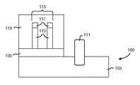
本発明の実施形態による集積回路デバイス100の形成が、図1から図8に示されるほぼ逐次的な製造ステップにおいて示される。ほぼ完成したデバイスの代替的な実施形態は図9から図11において示され、一般的な方法の流れの例は図10から図12に示される。図1に示すように、SOIウエハ101は、注入及び酸化による分離(SIMOX)、又はウエハ・ボンディング及びエッチ・バック、又は当該技術分野において一般に用いられる周知の技術のような周知の技術を用いて形成される。SOIウエハ101は、基板103の上の埋め込み分離層105の上にシリコン層115を含む。埋め込み分離層105は絶縁材料を含むが、埋め込み酸化物以外のいずれかの種類の埋め込み絶縁体を、埋め込み分離層105の代替物として用いることができる。埋め込み分離層105は、極めて薄い、約20ないし2000Åであることが好ましい。
The formation of
一実施形態においては、基板103は、単結晶シリコン層を含む。或いは、基板103は、シリコン(Si)、ゲルマニウム(Ge)、ガリウムリン(GaP)、ヒ化インジウム(InAs)、リン化インジウム(InP)、シリコン・ゲルマニウム(SiGe)、ヒ化ガリウム(GaAs)、又は他のIII/V族化合物を含むが、これらに限定されるものではない、任意の適切な半導体材料を含むことができる。基板103の反転を防ぐために、基板103の一部分は、低濃度ドープのウェル領域104、106を含む。さらに、高濃度ドープの逆型ウェル領域108、110が、基板103に形成される。当業者であれば、ウェル領域104、106、108、110は、対応するNウェル及び/又はPウェル領域として具体化できることを容易に理解するであろう。さらに、逆型ウェル領域104、106、108、110は、高エネルギー・イオン注入及びアニール法ような任意の周知の技術を用いて形成することができる。さらに、当業者であれは、逆型ウェル領域104、106、108、110は後に続く処理ステップに残るが、本発明の実施形態によって提供される他の関連する特徴を曖昧にしないように、逆型ウェル領域104、106、108、110は、図に示される構造に存在するが、図2から図11には示されないことを理解するであろう。低濃度ドープのウェルに対する典型的なドーズ量は、cm3当たり約1×1014から5×1015であり、高濃度ドープのウェルに対するドーズ量は、cm3当たり約3×1017から8×1018である。図2に示すように、ハードマスク膜107がシリコン層115の上に堆積される。その後、適当な異方性エッチングが行われ、ハードマスク膜107、シリコン層115、埋め込み分離層105、及び下にある基板103の一部がエッチングにより取り除かれ、これによって、デバイス100に狭い間隙109が形成される。次に、図3は、誘電体層111が、間隙109を埋めることを含み、ハードマスク膜107上に堆積された後のICデバイス100を示す。誘電体層111は、後に浅いトレンチ分離領域(STI)111(より具体的に図4に図示する)になるものを形成して、集積回路100における種々のデバイス間に電気的遮蔽を提供する。
In one embodiment, the
図4に示すように、ハードマスク膜107及び過剰な誘電体層111が適当な化学工程により剥離され、これによって、凹状STI領域111が形成される。STI領域111は、本発明の第一の実施形態による集積回路100に組み込まれる。しかし、(図9から図11に示す)本発明の第二の実施形態による集積回路102は、STI領域なしで組み立てることができる。従って、ハードマスク膜107の堆積を含むSTI領域111の形成、後に続く誘電体層111のエッチング及び堆積を含む処理ステップは、本発明の第二の実施形態の製造には含まれない。
As shown in FIG. 4, the
次に、図5に示すように、第1のFinFET誘電体層としての誘電キャップ層117が、堆積され、マスクされ、及びエッチングされる。さらに、シリコン層115が、このハードマスク膜117を使用してエッチングされる。シリコン層115及び誘電体層117が共同してフィン型構造体113を形成する。その後、図6に示すように、埋め込み分離層105の一部分を露光し、フィン型構造体113を保護するようにレジスト層119がマスクされる。膜119は、埋め込み分離層105のエッチングを可能にするようにマスクされ露光されるレジスト像を含むことが好ましい。その後、エッチング工程が行われ、これによって、膜119により保護されなてい埋め込み分離層105の部分(すなわち、デバイス100の平坦領域)が取り除かれて、下にある基板103が露光されるようになる。
Next, as shown in FIG. 5, a
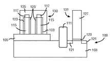
膜119が、適当な化学工程によって剥離された後で、図7に示すように、窒化物を含むことができる薄い、第1のFinFET誘電体層としての誘電体層123(例えば、約10ないし40Åの厚さ)が、デバイス100上に、より具体的には、シリコン層115、誘電体層117、シリコン基板103の全ての露光領域、及びソース/ドレイン接合部121(図8に示す)の上に、熱成長される。シリコン層115を取り囲む誘電体層123は、フィン型構造体113のためのゲート誘電体として機能し、基板103上の誘電体層123は、ゲート誘電体123として機能する。
After
図8は、好ましくはポリシリコン又はシリコン・ゲルマニウム材料を含むゲート材料125、127がデバイス100の上に堆積された後のデバイス100の第一の実施形態を示す。デバイス100は、次に、一つのステップでゲート材料125、127を平坦化するように化学機械研磨工程(CMP)を受け、これによって多数の処理ステップが省かれ、FETゲート127及びFinFETゲート125は同様な高さに構成される。FET及びFINFETゲート127、125はそれぞれ、次に、既知のリソグラフィー技術を用いてパターン形成されエッチングされて、ゲート材料125、127の一部が反応性イオンエッチング(RIE)により選択的に取り除かれて、FinFETゲート電極125及びFETゲート電極127を形成する。さらに、誘電体層123の露光部分もまた、エッチング工程中に取り除かれる。131は平坦型電界効果トランジスタ(FET)である。
FIG. 8 shows a first embodiment of the
さらに、図9に示されるように、ソース/ドレイン注入接合部121(間にチャネル領域(図示せず)をもつ)が基板103に形成される。同様に、ソース/ドレイン注入接合部122(図10)(間にチャネル領域(図示せず)をもつ)もまた、ソース/ドレイン注入接合部121が基板103に形成されるのと同時に、FinFETゲート125の両側(図10)に形成される。ソース/ドレイン接合部122は、本発明の第二の実施形態に対応する図10及び図11において最も良く見られ、第一の実施形態と同様な構成も提供されている。ソース/ドレイン接合部121、122の形成は、製造シーケンスのいずれかの適当な時点で生じることができる。さらに、ソース/ドレイン接合部121、122の形成は、特定の性能要求に調整されたいずれかの既知の方法を用いて達成することができる。そのようなものとして、種々のレベルの複雑さを有するソース/ドレイン接合部121、122の形成のための多くの方法がある。本発明の幾つかの実施形態においては、ソース/ドレイン接合部121、122は、低濃度ドープされ、イオン注入法を用いて形成することができる。例えば、NFETに対しては、通常、リン(P)、ヒ素(As)、アンチモン(Sb)又は他の適当な材料を、1から5keVまでの範囲、及び5×1014から2×1015cm−2までドーズ量でソース/ドレイン注入部121、122に用いることができる。同様に、PFETに対しては、通常、ホウ素(B)、インジウム(In)、ガリウム(Ga)又は他の適当な材料を、0.5から3keVまでの範囲、及び5×1014から2×1015cm−2までのドーズ量でソース/ドレイン注入部121、122に用いることができる。
Further, as shown in FIG. 9, a source / drain injection junction 121 (having a channel region (not shown) therebetween) is formed on the
さらに、本発明の他の実施形態においては、延長部及びハロ注入部(図示せず)を形成して、短チャネル効果(SCE)を改善することができる。NFETに対しては、通常、ホウ素(B)、インジウム(In)、ガリウム(Ga)又は他の適当な材料を、5から15keVまでのエネルギー範囲、及び1×10¹³から8×1013cm−2までのドーズ量でハロ注入部に用いることができる。同様に、PFETに対しては、通常、リン(P)、ヒ素(As)、アンチモン(Sb)又は他の適当な材料を、20から45keVまでのエネルギー範囲、及び1×10¹³から8×1013cm−2までのドーズ量でハロ注入部に用いることができる。 In addition, in other embodiments of the invention, extensions and halo implants (not shown) can be formed to improve short channel effects (SCE). For NFETs, typically boron (B), indium (In), gallium (Ga) or other suitable material is used in an energy range of 5 to 15 keV, and 1 × 10 13 to 8 × 10 13 cm −. It can be used for halo implants at doses up to 2 . Similarly, for PFETs, typically phosphorous (P), arsenic (As), antimony (Sb) or other suitable material is used in an energy range of 20 to 45 keV, and 1 × 10 13 to 8 × 10. It can be used for halo implants at doses up to 13 cm −2 .
図9から図11は、ゲート電極125及びFETゲート電極127が形成された後のデバイス100の第二の実施形態を示す。ここでも、第一の実施形態と第二の実施形態との間の違いは、第一の実施形態のデバイス100は隆起したSTI領域111を含むが、第二の実施形態のデバイス102はトレンチ分離領域を含まないことである。ゲート材料125、127は、平坦型FET131(埋め込み分離層105が取り除かれた領域)及びFINFET領域130(図11)の上に堆積され、一度のエッチングで、両方の領域がエッチングされる。従って、本発明の実施形態によって提供される製造技術は、一般的なSOI FINFET工程に対して小さな修正のみを必要とし、簡便な製造工程をもたらし、平坦型FET構造体131及びFinFET構造体130においては、ゲートのステップ高さの違いは極わずかである。図10及び図11は、特に第二の実施形態を例示するものであるが、当業者であれば、図10及び図11は、第一の実施形態に提供されるSTI領域を含まないことを除いては、第一の実施形態の代替的な図を同様に提供することを容易に理解するであろう。さらに、図11における点線AA−AA’は、図9の断面図の境界を提供する。
9-11 illustrate a second embodiment of the
平坦型FET131及びFinFET構造体130の形成後、デバイス100、102は、デバイスの高さの上方に形成される、相互接続部、コンタクト、配線層等(図示せず)を含む、残りの集積回路構造体の形成のために従来の処理を受ける。さらに、従来の製造技術により、幾つかのダマシン層(図示せず)をデバイス100、102の上に形成することができる。
After the formation of the
図1から図11に示される構造体は、従来の手法とは対照的に、こうしたデバイスを埋め込み分離層105の上方領域ではなく、基板103に配置することによって、より良好な温度制御を実現する。さらに、アナログ及びESDデバイスは、この改良された温度制御から利益を得る。基板103に内蔵されたデバイスは、さらに、改良された電源管理のための基板バイアスを支持することができる。さらに、図1から図11までに示される構造体の処理は、はるかに複雑ではなくなっており、従来のデバイス及び処理と比較すると、削減された費用で実行でき、より優れた温度制御を提供することができる。
The structure shown in FIGS. 1-11 provides better temperature control by placing such a device on the
本発明の別の実施形態は、図1から図11までに示される部品を指す説明を含む図12から図14までのフローチャートに示され、図12は、集積回路100を形成する方法を示し、この方法は、基板103を準備するステップ(201)と、埋め込み分離層105を基板上に形成するステップ(203)と、半導体層115を埋め込み分離層105に結合するステップ(205)と、を含む。この方法の次の段階は、ウェル領域104、106、108、110を基板103に構成するステップ(207)と、随意的にSTI領域111を基板103に構成するステップ(209)と、埋め込み分離層105の一部分を除去するステップ(211)と、FinFET130を埋め込み分離層105上に形成し、同時に、平坦型FET131を基板103に形成するステップ(213)と、を含む。その後、この方法は、FETゲート127及びFinFETゲート125を平坦化するステップ(215)を含む。一実施形態においては、埋め込み分離層105は、埋め込み酸化物から形成される。
Another embodiment of the present invention is shown in the flowchart of FIGS. 12-14, including a description referring to the components shown in FIGS. 1-11, which shows a method of forming an
図13のフローチャートに示されるように、FinFET130を形成する(213)工程は、第1のFinFET誘電体層117を半導体層115上に形成するステップ(223)と、埋め込み分離層105上の半導体層115をエッチングするステップ(225)であって、その半導体層115は側壁を含むステップ、と、埋め込み分離層の一部分を選択的に除去するステップ(227)と、第2のFinFET誘電体層123を半導体層115の側壁の各々に沿って及び基板103の上に構成するステップ(229)と、FinFETゲート領域125を第1の誘電体層及び第2の誘電体層117、123の上に形成するステップ(231)と、FinFETソース/ドレイン領域122をFinFETゲート領域125の両側に形成するステップ(233)と、を含む。
As shown in the flowchart of FIG. 13, the step (213) of forming the
図14のフローチャートに示されるように、(FinFET130の形成と同時に生じる)平坦型FET131を形成する(213)工程は、FETゲート誘電体層123を基板103上に形成するステップ(241)と、FETゲート領域127をFETゲート誘電体層123上に形成するステップ(243)であって、FETゲート誘電体層123が、FETゲート領域127に隣接する、ステップと、FETソース/ドレイン領域121を基板103に形成するステップ(245)と、を含む。さらに、FETゲート誘電体層123は、FETゲート領域127と基板103との間に形成される。さらに、FinFETゲート領域125及びFETゲート領域127の各々は、ポリシリコンを含む。
As shown in the flowchart of FIG. 14, the step (213) of forming the flat FET 131 (which occurs simultaneously with the formation of the FinFET 130) includes the step (241) of forming the FET
基板103における平坦型FET131をFinFET SOIデバイス130と一体化することは、論理ゲート、メモリ・セル、アナログ回路、ESDデバイス、キャパシタ、レジスタ等を含む、多くの種類のICデバイスを生成するのに用いることができる。本発明の実施形態により与えられる別の利点は、平坦型FET131として基板103に組み込むことによる主要なデバイスの温度制御能力である。
Integrating the
一般に、本発明の実施形態は、基板103と、基板103上の埋め込み分離層105と、埋め込み分離層105上のFinFET130と、基板103に一体化されたFET131とを含み、FETゲート127がFinFETゲート125に対して高さの違いは極くわずかである、構造体100、102を提供する。本発明の実施形態は、実施するのが容易な一体化技術を提供し、これによって、平坦型FET131がFinFETデバイス130に組み込まれ形成されて、FETゲート127及びFinFETゲート125が、1つの製造ステップで形成されるようになる。例えば、FETゲート材料127及びFinFETゲート材料125の堆積は同時に生じ、FETゲート材料127及びFinFETゲート材料125の平坦化は同時に生じる。FETゲート127及びFinFETゲート125は、同じ上方の高さに平坦化され、これにより、付加的なリソグラフィー及びエッチング工程の必要性を不要にして、製造ステップ数が減り、結果として製造費全体の削減がもたらされる。
In general, embodiments of the present invention include a
上記の特定の実施形態の説明は、現行の知識を加えることによって、類概念から離れることなく、他者がこうした特定の実施形態を種々の用途のために修正する及び/又は適応させることができ、従って、こうした適応及び修正は、開示された実施形態の意味及び等価物の範囲内で理解されるべきであり、そのように意図される本発明の一般的な性質を完全に明らかにするであろう。ここで採用される専門語又は術語は説明の目的のためであって、制限するためではないことが理解される。従って、本発明の実施形態は好ましい実施形態によって説明されるが、当業者であれば、本発明の実施形態は、添付の特許請求の範囲の精神及び範囲内の修正形態により実施できることを認識するであろう。 The above description of particular embodiments allows the others to modify and / or adapt these particular embodiments for various applications without departing from the analogy by adding current knowledge. Accordingly, such adaptations and modifications are to be understood within the meaning and equivalents of the disclosed embodiments and should fully disclose the general nature of the invention as intended. I will. It is understood that the terminology or terminology employed herein is for purposes of illustration and not limitation. Thus, while embodiments of the invention are described by preferred embodiments, those skilled in the art will recognize that embodiments of the invention can be practiced with modification within the spirit and scope of the appended claims. Will.
100:集積回路デバイス
101:SOIウエハ
102:デバイス
103:基板
104、106、108、110:逆型ウェル領域
105:埋め込み分離層
111:浅いトレンチ分離領域
115:シリコン層
125:FinFETゲート
127:FETゲート
130:FinFET
131:平坦型FET
100: integrated circuit device 101: SOI wafer 102: device 103:
131: Flat FET
Claims (3)
前記基板上の埋め込み分離層と、
前記埋め込み分離層上のフィン型電解効果トランジスタ(FinFET)と、
前記基板における平坦型電解効果トランジスタ(FET)であって、前記FETのゲート領域が前記FinFETのゲート領域と同様な高さに形成される、平坦型電解効果トランジスタ(FET)と、
を含む構造体。A substrate,
A buried isolation layer on the substrate;
A fin-type field effect transistor (FinFET) on the buried isolation layer;
A flat field effect transistor (FET) in the substrate, wherein the gate region of the FET is formed at the same height as the gate region of the FinFET;
A structure containing
前記基板上の埋め込み分離層と、
前記埋め込み分離層上の半導体層と、
を含むシリコン・オン・インシュレータ(SOI)ウエハと、
前記埋め込み分離層上のフィン型電解効果トランジスタ(FinFET)と、
前記基板に組み込まれた平坦型電解効果トランジスタ(FET)であって、前記FETのゲート領域が前記FinFETのゲート領域と同様な高さに形成される、平坦型電解効果トランジスタ(FET)と、
を含む構造体。A substrate,
A buried isolation layer on the substrate;
A semiconductor layer on the buried isolation layer;
A silicon-on-insulator (SOI) wafer including:
A fin-type field effect transistor (FinFET) on the buried isolation layer;
A flat field effect transistor (FET) embedded in the substrate, wherein the gate region of the FET is formed at the same height as the gate region of the FinFET;
A structure containing
基板を準備するステップと、
埋め込み分離層を前記基板上に形成するステップと、
半導体層を前記埋め込み分離層に結合するステップと、
第1の誘電体層を前記半導体層上に形成した後、該第1の誘電体層をハードマスクとして該半導体層をエッチングしてフィン型構造体を形成するステップと、
前記埋め込み分離層の一部分を選択的に除去して前記基板を露出させるステップと、
前記フィン型構造体の側壁の上及び露出した前記基板の上に第2の誘電体層を形成するステップと、
前記第1の誘電体層の上及び前記第2の誘電体層の上にゲート材料を同時に堆積するステップと、
前記ゲート材料を同時に平坦化してFinFETのゲート領域とFETのゲート領域とを同様な高さに形成するステップと、
含む方法。A method for forming a flat field effect transistor (FET) substrate device integrated with a fin field effect transistor (FinFET) comprising:
Preparing a substrate;
Forming a buried isolation layer on the substrate;
Coupling a semiconductor layer to the buried isolation layer;
Forming a first dielectric layer on the semiconductor layer, and then etching the semiconductor layer using the first dielectric layer as a hard mask to form a fin-type structure;
Selectively removing a portion of the buried isolation layer to expose the substrate;
Forming a second dielectric layer on sidewalls of the fin structure and on the exposed substrate;
Simultaneously depositing a gate material on the first dielectric layer and on the second dielectric layer;
Simultaneously planarizing the gate material to form a gate region of the FinFET and a gate region of the FET at similar heights;
Including methods.
Applications Claiming Priority (3)
| Application Number | Priority Date | Filing Date | Title |
|---|---|---|---|
| US10/711,974 US6949768B1 (en) | 2004-10-18 | 2004-10-18 | Planar substrate devices integrated with finfets and method of manufacture |
| US10/711,974 | 2004-10-18 | ||
| PCT/US2005/036471 WO2006044349A2 (en) | 2004-10-18 | 2005-10-11 | Planar substrate devices integrated with finfets and method of manufacture |
Publications (3)
| Publication Number | Publication Date |
|---|---|
| JP2008517464A JP2008517464A (en) | 2008-05-22 |
| JP2008517464A5 JP2008517464A5 (en) | 2008-09-04 |
| JP4711446B2 true JP4711446B2 (en) | 2011-06-29 |
Family
ID=34992630
Family Applications (1)
| Application Number | Title | Priority Date | Filing Date |
|---|---|---|---|
| JP2007536791A Expired - Fee Related JP4711446B2 (en) | 2004-10-18 | 2005-10-11 | Flat substrate device integrated with FINFET and method of manufacturing the same |
Country Status (7)
| Country | Link |
|---|---|
| US (2) | US6949768B1 (en) |
| EP (1) | EP1805795A4 (en) |
| JP (1) | JP4711446B2 (en) |
| KR (2) | KR20100105779A (en) |
| CN (1) | CN100533758C (en) |
| TW (1) | TWI380343B (en) |
| WO (1) | WO2006044349A2 (en) |
Families Citing this family (98)
| Publication number | Priority date | Publication date | Assignee | Title |
|---|---|---|---|---|
| US7719043B2 (en) * | 2004-07-12 | 2010-05-18 | Nec Corporation | Semiconductor device with fin-type field effect transistor and manufacturing method thereof. |
| JP2006049627A (en) * | 2004-08-05 | 2006-02-16 | Toshiba Corp | Semiconductor device and its manufacturing method |
| KR100612419B1 (en) * | 2004-10-19 | 2006-08-16 | 삼성전자주식회사 | Semiconductor devices having a fin transistor and a plannar transistor and methods of forming the same |
| JP2006261188A (en) * | 2005-03-15 | 2006-09-28 | Seiko Epson Corp | Semiconductor device and its manufacturing method |
| US7920544B2 (en) * | 2005-03-28 | 2011-04-05 | Qualcomm Incorporated | Method and apparatus for enhancing signal-to-noise ratio of position location measurements |
| JP2007018588A (en) * | 2005-07-06 | 2007-01-25 | Toshiba Corp | Semiconductor storage device and method of driving the semiconductor storage device |
| WO2007049170A1 (en) * | 2005-10-25 | 2007-05-03 | Nxp B.V. | Finfet transistors |
| US7512017B2 (en) * | 2005-12-21 | 2009-03-31 | Intel Corporation | Integration of planar and tri-gate devices on the same substrate |
| US7264743B2 (en) * | 2006-01-23 | 2007-09-04 | Lam Research Corporation | Fin structure formation |
| JP2007294857A (en) * | 2006-03-28 | 2007-11-08 | Elpida Memory Inc | Semiconductor device and manufacturing method therefor |
| US7803670B2 (en) * | 2006-07-20 | 2010-09-28 | Freescale Semiconductor, Inc. | Twisted dual-substrate orientation (DSO) substrates |
| US7456471B2 (en) * | 2006-09-15 | 2008-11-25 | International Business Machines Corporation | Field effect transistor with raised source/drain fin straps |
| US8368144B2 (en) * | 2006-12-18 | 2013-02-05 | Infineon Technologies Ag | Isolated multigate FET circuit blocks with different ground potentials |
| US8492796B2 (en) * | 2007-03-13 | 2013-07-23 | Infineon Technologies Ag | MuGFET switch |
| US7923337B2 (en) * | 2007-06-20 | 2011-04-12 | International Business Machines Corporation | Fin field effect transistor devices with self-aligned source and drain regions |
| JP4459257B2 (en) * | 2007-06-27 | 2010-04-28 | 株式会社東芝 | Semiconductor device |
| US9064963B2 (en) * | 2007-09-28 | 2015-06-23 | Infineon Technologies Ag | Semiconductor structure |
| US8329564B2 (en) * | 2007-10-26 | 2012-12-11 | International Business Machines Corporation | Method for fabricating super-steep retrograde well MOSFET on SOI or bulk silicon substrate, and device fabricated in accordance with the method |
| US7772651B2 (en) * | 2008-01-11 | 2010-08-10 | International Business Machines Corporation | Semiconductor-on-insulator high-voltage device structures, methods of fabricating such device structures, and design structures for high-voltage circuits |
| US7790543B2 (en) * | 2008-01-11 | 2010-09-07 | International Business Machines Corporation | Device structures for a metal-oxide-semiconductor field effect transistor and methods of fabricating such device structures |
| US7790524B2 (en) * | 2008-01-11 | 2010-09-07 | International Business Machines Corporation | Device and design structures for memory cells in a non-volatile random access memory and methods of fabricating such device structures |
| US7786535B2 (en) * | 2008-01-11 | 2010-08-31 | International Business Machines Corporation | Design structures for high-voltage integrated circuits |
| WO2009110048A1 (en) * | 2008-02-15 | 2009-09-11 | 日本ユニサンティスエレクトロニクス株式会社 | Semiconductor devuce and manufacturing method thereof |
| US8211786B2 (en) * | 2008-02-28 | 2012-07-03 | International Business Machines Corporation | CMOS structure including non-planar hybrid orientation substrate with planar gate electrodes and method for fabrication |
| US8331068B2 (en) * | 2009-02-19 | 2012-12-11 | Taiwan Semiconductor Manufacturing Company, Ltd. | ESD protection for FinFETs |
| US8305829B2 (en) * | 2009-02-23 | 2012-11-06 | Taiwan Semiconductor Manufacturing Company, Ltd. | Memory power gating circuit for controlling internal voltage of a memory array, system and method for controlling the same |
| US8305790B2 (en) * | 2009-03-16 | 2012-11-06 | Taiwan Semiconductor Manufacturing Company, Ltd. | Electrical anti-fuse and related applications |
| US8957482B2 (en) * | 2009-03-31 | 2015-02-17 | Taiwan Semiconductor Manufacturing Company, Ltd. | Electrical fuse and related applications |
| US8912602B2 (en) * | 2009-04-14 | 2014-12-16 | Taiwan Semiconductor Manufacturing Company, Ltd. | FinFETs and methods for forming the same |
| US7968971B2 (en) * | 2009-06-22 | 2011-06-28 | Taiwan Semiconductor Manufacturing Co., Ltd. | Thin-body bipolar device |
| US8461015B2 (en) * | 2009-07-08 | 2013-06-11 | Taiwan Semiconductor Manufacturing Company, Ltd. | STI structure and method of forming bottom void in same |
| US8440517B2 (en) | 2010-10-13 | 2013-05-14 | Taiwan Semiconductor Manufacturing Company, Ltd. | FinFET and method of fabricating the same |
| US8759943B2 (en) | 2010-10-08 | 2014-06-24 | Taiwan Semiconductor Manufacturing Company, Ltd. | Transistor having notched fin structure and method of making the same |
| US8482073B2 (en) * | 2010-03-25 | 2013-07-09 | Taiwan Semiconductor Manufacturing Company, Ltd. | Integrated circuit including FINFETs and methods for forming the same |
| US8298925B2 (en) | 2010-11-08 | 2012-10-30 | Taiwan Semiconductor Manufacturing Company, Ltd. | Mechanisms for forming ultra shallow junction |
| US8629478B2 (en) * | 2009-07-31 | 2014-01-14 | Taiwan Semiconductor Manufacturing Company, Ltd. | Fin structure for high mobility multiple-gate transistor |
| US8497528B2 (en) | 2010-05-06 | 2013-07-30 | Taiwan Semiconductor Manufacturing Company, Ltd. | Method for fabricating a strained structure |
| US8472227B2 (en) * | 2010-01-27 | 2013-06-25 | Taiwan Semiconductor Manufacturing Company, Ltd. | Integrated circuits and methods for forming the same |
| US8623728B2 (en) | 2009-07-28 | 2014-01-07 | Taiwan Semiconductor Manufacturing Company, Ltd. | Method for forming high germanium concentration SiGe stressor |
| US8980719B2 (en) | 2010-04-28 | 2015-03-17 | Taiwan Semiconductor Manufacturing Company, Ltd. | Methods for doping fin field-effect transistors |
| US9484462B2 (en) * | 2009-09-24 | 2016-11-01 | Taiwan Semiconductor Manufacturing Company, Ltd. | Fin structure of fin field effect transistor |
| US9112052B2 (en) | 2009-10-14 | 2015-08-18 | Taiwan Semiconductor Manufacturing Company, Ltd. | Voids in STI regions for forming bulk FinFETs |
| US8519481B2 (en) | 2009-10-14 | 2013-08-27 | Taiwan Semiconductor Manufacturing Company, Ltd. | Voids in STI regions for forming bulk FinFETs |
| US20110097867A1 (en) * | 2009-10-22 | 2011-04-28 | Taiwan Semiconductor Manufacturing Company, Ltd. | Method of controlling gate thicknesses in forming fusi gates |
| US8436404B2 (en) | 2009-12-30 | 2013-05-07 | Intel Corporation | Self-aligned contacts |
| US9040393B2 (en) | 2010-01-14 | 2015-05-26 | Taiwan Semiconductor Manufacturing Company, Ltd. | Method of forming semiconductor structure |
| US8513723B2 (en) * | 2010-01-19 | 2013-08-20 | International Business Machines Corporation | Method and structure for forming high performance MOS capacitor along with fully depleted semiconductor on insulator devices on the same chip |
| CN102315268B (en) * | 2010-07-01 | 2013-07-10 | 中国科学院微电子研究所 | Semiconductor device and making method thereof |
| US8354319B2 (en) | 2010-10-15 | 2013-01-15 | International Business Machines Corporation | Integrated planar and multiple gate FETs |
| US8603924B2 (en) | 2010-10-19 | 2013-12-10 | Taiwan Semiconductor Manufacturing Company, Ltd. | Methods of forming gate dielectric material |
| US8769446B2 (en) | 2010-11-12 | 2014-07-01 | Taiwan Semiconductor Manufacturing Company, Ltd. | Method and device for increasing fin device density for unaligned fins |
| US8592915B2 (en) | 2011-01-25 | 2013-11-26 | Taiwan Semiconductor Manufacturing Company, Ltd. | Doped oxide for shallow trench isolation (STI) |
| US8877602B2 (en) | 2011-01-25 | 2014-11-04 | Taiwan Semiconductor Manufacturing Company, Ltd. | Mechanisms of doping oxide for forming shallow trench isolation |
| CN102651321B (en) * | 2011-02-25 | 2015-03-04 | 中国科学院微电子研究所 | Manufacturing method for semiconductor devices |
| US8431453B2 (en) | 2011-03-31 | 2013-04-30 | Taiwan Semiconductor Manufacturing Company, Ltd. | Plasma doping to reduce dielectric loss during removal of dummy layers in a gate structure |
| CN102842507B (en) * | 2011-06-24 | 2015-08-19 | 中国科学院微电子研究所 | The preparation method of semiconductor field effect transistor |
| CN102842508B (en) * | 2011-06-24 | 2015-03-04 | 中国科学院微电子研究所 | Manufacturing method for semiconductor field effect transistor |
| US8778744B2 (en) * | 2011-06-24 | 2014-07-15 | Institute of Microelectronics, Chinese Academy of Sciences | Method for manufacturing semiconductor field effect transistor |
| US8842945B2 (en) * | 2011-08-09 | 2014-09-23 | Soitec | Methods of forming three dimensionally integrated semiconductor systems including photoactive devices and semiconductor-on-insulator substrates |
| CN103022038B (en) * | 2011-09-21 | 2015-06-10 | 中国科学院微电子研究所 | Static random access memory (SRAM) unit and manufacturing method thereof |
| US9397104B2 (en) | 2011-09-21 | 2016-07-19 | Institute of Microelectronics, Chinese Academy of Sciences | SRAM cell and method for manufacturing the same |
| DE112011105996B4 (en) * | 2011-12-22 | 2023-11-16 | Intel Corporation | Semiconductor component with a narrowed semiconductor body |
| US20130173214A1 (en) * | 2012-01-04 | 2013-07-04 | International Business Machines Corporation | Method and structure for inline electrical fin critical dimension measurement |
| US8587068B2 (en) | 2012-01-26 | 2013-11-19 | International Business Machines Corporation | SRAM with hybrid FinFET and planar transistors |
| US8466012B1 (en) * | 2012-02-01 | 2013-06-18 | International Business Machines Corporation | Bulk FinFET and SOI FinFET hybrid technology |
| US8916426B2 (en) | 2012-03-27 | 2014-12-23 | International Business Machines Corporation | Passive devices for FinFET integrated circuit technologies |
| US8692291B2 (en) * | 2012-03-27 | 2014-04-08 | International Business Machines Corporation | Passive devices for FinFET integrated circuit technologies |
| US9219056B2 (en) | 2012-03-27 | 2015-12-22 | International Business Machines Corporation | Passive devices for FinFET integrated circuit technologies |
| US9583398B2 (en) | 2012-06-29 | 2017-02-28 | Taiwan Semiconductor Manufacturing Company, Ltd. | Integrated circuit having FinFETS with different fin profiles |
| US8586449B1 (en) | 2012-08-14 | 2013-11-19 | International Business Machines Corporation | Raised isolation structure self-aligned to fin structures |
| US8987823B2 (en) * | 2012-11-07 | 2015-03-24 | International Business Machines Corporation | Method and structure for forming a localized SOI finFET |
| US8759874B1 (en) * | 2012-11-30 | 2014-06-24 | Stmicroelectronics, Inc. | FinFET device with isolated channel |
| US8890249B2 (en) | 2012-11-30 | 2014-11-18 | International Business Machines Corporation | Bulk FinFET ESD device |
| US9054124B2 (en) | 2012-12-14 | 2015-06-09 | International Business Machines Corporation | Electrostatic discharge resistant diodes |
| FR3005309B1 (en) | 2013-05-02 | 2016-03-11 | Commissariat Energie Atomique | NANOWELL AND PLANNER TRANSISTORS COINTEGRATED ON SUBSTRATE SOI UTBOX |
| US8963259B2 (en) * | 2013-05-31 | 2015-02-24 | Globalfoundries Inc. | Device isolation in finFET CMOS |
| US8957478B2 (en) | 2013-06-24 | 2015-02-17 | International Business Machines Corporation | Semiconductor device including source/drain formed on bulk and gate channel formed on oxide layer |
| US9515184B2 (en) * | 2013-09-12 | 2016-12-06 | Taiwan Semiconductor Manufacturing Company Limited | Semiconductor arrangement with multiple-height fins and substrate trenches |
| US9048123B2 (en) | 2013-09-19 | 2015-06-02 | International Business Machines Corporation | Interdigitated finFETs |
| US9312272B2 (en) | 2013-11-27 | 2016-04-12 | Globalfoundries Inc. | Implementing buried FET utilizing drain of finFET as gate of buried FET |
| US9059020B1 (en) | 2013-12-02 | 2015-06-16 | International Business Machins Corporation | Implementing buried FET below and beside FinFET on bulk substrate |
| US9099570B2 (en) * | 2013-12-05 | 2015-08-04 | Stmicroelectronics, Inc. | Method for the formation of dielectric isolated fin structures for use, for example, in FinFET devices |
| US20150171217A1 (en) * | 2013-12-12 | 2015-06-18 | Texas Instruments Incorporated | Design and integration of finfet device |
| US9443851B2 (en) * | 2014-01-03 | 2016-09-13 | Samsung Electronics Co., Ltd. | Semiconductor devices including finFETs and local interconnect layers and methods of fabricating the same |
| US9129863B2 (en) | 2014-02-11 | 2015-09-08 | International Business Machines Corporation | Method to form dual channel group III-V and Si/Ge FINFET CMOS |
| US9123585B1 (en) | 2014-02-11 | 2015-09-01 | International Business Machines Corporation | Method to form group III-V and Si/Ge FINFET on insulator |
| KR102171023B1 (en) * | 2014-07-21 | 2020-10-29 | 삼성전자주식회사 | Method of fabricating semiconductor devices |
| KR102245133B1 (en) | 2014-10-13 | 2021-04-28 | 삼성전자 주식회사 | Semiconductor device comprising finFETs(fin Field Effect Transistors) of different gate structures and method for fabricating the same |
| US9391065B1 (en) * | 2015-06-29 | 2016-07-12 | Globalfoundries Inc. | Electrostatic discharge and passive structures integrated in a vertical gate fin-type field effect diode |
| CN108243625B (en) * | 2015-11-03 | 2022-04-22 | 硅存储技术公司 | Split-gate non-volatile flash memory cell with metal gate and method of making the same |
| KR102402771B1 (en) | 2015-12-11 | 2022-05-26 | 삼성전자주식회사 | Semiconductor device and method for fabricating the same |
| US9899378B2 (en) | 2015-12-14 | 2018-02-20 | International Business Machines Corporation | Simultaneously fabricating a high voltage transistor and a finFET |
| EP3182461B1 (en) * | 2015-12-16 | 2022-08-03 | IMEC vzw | Method for fabricating finfet technology with locally higher fin-to-fin pitch |
| US9748389B1 (en) * | 2016-03-25 | 2017-08-29 | Taiwan Semiconductor Manufacturing Co., Ltd. | Method for semiconductor device fabrication with improved source drain epitaxy |
| US10290654B2 (en) | 2016-05-20 | 2019-05-14 | Globalfoundries Inc. | Circuit structures with vertically spaced transistors and fabrication methods |
| US10147802B2 (en) * | 2016-05-20 | 2018-12-04 | Globalfoundries Inc. | FINFET circuit structures with vertically spaced transistors and fabrication methods |
| US9646962B1 (en) | 2016-10-05 | 2017-05-09 | International Business Machines Corporation | Low leakage gate controlled vertical electrostatic discharge protection device integration with a planar FinFET |
| RU2670248C1 (en) * | 2017-09-05 | 2018-10-19 | Акционерное общество "Научно-исследовательский институт молекулярной электроники" | Method for forming local buried dielectric insulation region of active part of transistors with three-dimensional structure of shell (finfet) |
Citations (5)
| Publication number | Priority date | Publication date | Assignee | Title |
|---|---|---|---|---|
| JP2002057220A (en) * | 2000-08-11 | 2002-02-22 | Seiko Epson Corp | Semiconductor device and manufacturing method therefor |
| JP2003229575A (en) * | 2002-02-04 | 2003-08-15 | Hitachi Ltd | Integrated semiconductor device and manufacturing method therefor |
| JP2004214413A (en) * | 2002-12-27 | 2004-07-29 | Toshiba Corp | Semiconductor device |
| WO2005022637A1 (en) * | 2003-08-28 | 2005-03-10 | Nec Corporation | Semiconductor device having fin-type field effect transistors |
| WO2006006438A1 (en) * | 2004-07-12 | 2006-01-19 | Nec Corporation | Semiconductor device and manufacturing method thereof |
Family Cites Families (20)
| Publication number | Priority date | Publication date | Assignee | Title |
|---|---|---|---|---|
| JPH04179166A (en) * | 1990-11-09 | 1992-06-25 | Hitachi Ltd | Insulated gate semiconductor device and manufacture thereof |
| JP2789931B2 (en) * | 1991-05-27 | 1998-08-27 | 日本電気株式会社 | Semiconductor device |
| JP3462301B2 (en) * | 1995-06-16 | 2003-11-05 | 三菱電機株式会社 | Semiconductor device and manufacturing method thereof |
| US6140163A (en) * | 1997-07-11 | 2000-10-31 | Advanced Micro Devices, Inc. | Method and apparatus for upper level substrate isolation integrated with bulk silicon |
| WO1999033115A1 (en) * | 1997-12-19 | 1999-07-01 | Advanced Micro Devices, Inc. | Silicon-on-insulator configuration which is compatible with bulk cmos architecture |
| US6093585A (en) * | 1998-05-08 | 2000-07-25 | Lsi Logic Corporation | High voltage tolerant thin film transistor |
| US6252284B1 (en) | 1999-12-09 | 2001-06-26 | International Business Machines Corporation | Planarized silicon fin device |
| US6607950B2 (en) * | 2000-03-30 | 2003-08-19 | Interuniversitair Microelektronic Centrum (Imec) | MIS transistors with a metal gate and high-k dielectric and method of forming |
| US6720231B2 (en) | 2002-01-28 | 2004-04-13 | International Business Machines Corporation | Fin-type resistors |
| JP3782021B2 (en) * | 2002-02-22 | 2006-06-07 | 株式会社東芝 | Semiconductor device, semiconductor device manufacturing method, and semiconductor substrate manufacturing method |
| US6995412B2 (en) | 2002-04-12 | 2006-02-07 | International Business Machines Corporation | Integrated circuit with capacitors having a fin structure |
| US7074623B2 (en) * | 2002-06-07 | 2006-07-11 | Amberwave Systems Corporation | Methods of forming strained-semiconductor-on-insulator finFET device structures |
| EP1383166A3 (en) * | 2002-07-16 | 2006-10-11 | Interuniversitair Microelektronica Centrum ( Imec) | FIN field effect transistor device and a method for manufacturing such device |
| US6770516B2 (en) * | 2002-09-05 | 2004-08-03 | Taiwan Semiconductor Manufacturing Company | Method of forming an N channel and P channel FINFET device on the same semiconductor substrate |
| JP4546021B2 (en) * | 2002-10-02 | 2010-09-15 | ルネサスエレクトロニクス株式会社 | Insulated gate field effect transistor and semiconductor device |
| US6670516B1 (en) * | 2002-12-20 | 2003-12-30 | Uop Llc | Process for producing phenyl-alkanes using olefin isomerization and paraffin recycle |
| WO2004084292A1 (en) * | 2003-03-20 | 2004-09-30 | Matsushita Electric Industrial Co., Ltd. | Finfet-type semiconductor device and method for fabricating the same |
| US6844238B2 (en) * | 2003-03-26 | 2005-01-18 | Taiwan Semiconductor Manufacturing Co., Ltd | Multiple-gate transistors with improved gate control |
| US20050003592A1 (en) * | 2003-06-18 | 2005-01-06 | Jones A. Brooke | All-around MOSFET gate and methods of manufacture thereof |
| US7211864B2 (en) * | 2003-09-15 | 2007-05-01 | Seliskar John J | Fully-depleted castellated gate MOSFET device and method of manufacture thereof |
-
2004
- 2004-10-18 US US10/711,974 patent/US6949768B1/en active Active
-
2005
- 2005-08-09 US US11/200,271 patent/US7368354B2/en active Active
- 2005-10-11 EP EP05809789A patent/EP1805795A4/en not_active Withdrawn
- 2005-10-11 KR KR1020107018457A patent/KR20100105779A/en active IP Right Grant
- 2005-10-11 KR KR1020077008883A patent/KR100985639B1/en not_active IP Right Cessation
- 2005-10-11 TW TW094135386A patent/TWI380343B/en active
- 2005-10-11 JP JP2007536791A patent/JP4711446B2/en not_active Expired - Fee Related
- 2005-10-11 WO PCT/US2005/036471 patent/WO2006044349A2/en active Application Filing
- 2005-10-11 CN CNB2005800354842A patent/CN100533758C/en active Active
Patent Citations (5)
| Publication number | Priority date | Publication date | Assignee | Title |
|---|---|---|---|---|
| JP2002057220A (en) * | 2000-08-11 | 2002-02-22 | Seiko Epson Corp | Semiconductor device and manufacturing method therefor |
| JP2003229575A (en) * | 2002-02-04 | 2003-08-15 | Hitachi Ltd | Integrated semiconductor device and manufacturing method therefor |
| JP2004214413A (en) * | 2002-12-27 | 2004-07-29 | Toshiba Corp | Semiconductor device |
| WO2005022637A1 (en) * | 2003-08-28 | 2005-03-10 | Nec Corporation | Semiconductor device having fin-type field effect transistors |
| WO2006006438A1 (en) * | 2004-07-12 | 2006-01-19 | Nec Corporation | Semiconductor device and manufacturing method thereof |
Also Published As
| Publication number | Publication date |
|---|---|
| US7368354B2 (en) | 2008-05-06 |
| WO2006044349A9 (en) | 2007-08-16 |
| US6949768B1 (en) | 2005-09-27 |
| US20060084212A1 (en) | 2006-04-20 |
| JP2008517464A (en) | 2008-05-22 |
| KR20070064346A (en) | 2007-06-20 |
| TWI380343B (en) | 2012-12-21 |
| TW200614334A (en) | 2006-05-01 |
| CN100533758C (en) | 2009-08-26 |
| KR20100105779A (en) | 2010-09-29 |
| KR100985639B1 (en) | 2010-10-05 |
| EP1805795A2 (en) | 2007-07-11 |
| WO2006044349A2 (en) | 2006-04-27 |
| EP1805795A4 (en) | 2010-10-06 |
| WO2006044349A3 (en) | 2007-06-07 |
| CN101103463A (en) | 2008-01-09 |
Similar Documents
| Publication | Publication Date | Title |
|---|---|---|
| JP4711446B2 (en) | Flat substrate device integrated with FINFET and method of manufacturing the same | |
| TWI596711B (en) | Cointegration of bulk and soi semiconductor devices | |
| CN108807381B (en) | FINFET device and method of fabricating the same | |
| US8003458B2 (en) | Methods of manufacturing a semiconductor device with active regions of different heights | |
| US20080248615A1 (en) | Cmos structure for body ties in ultra-thin soi (utsoi) substrates | |
| US10748893B2 (en) | Electrostatic discharge devices and methods of manufacture | |
| US10170364B2 (en) | Stress memorization technique for strain coupling enhancement in bulk finFET device | |
| US6469350B1 (en) | Active well schemes for SOI technology | |
| US7939395B2 (en) | High-voltage SOI MOS device structure and method of fabrication | |
| KR101354397B1 (en) | Differential nitride pullback to create differential nfet to pfet divots for improved performance versus leakage | |
| TW201926711A (en) | Laterally double diffused metal oxide semiconductor (LDMOS) device on fully depleted silicon on insulator (FDSOI) enabling high input voltage | |
| US9324869B1 (en) | Method of forming a semiconductor device and resulting semiconductor devices | |
| US11545483B2 (en) | Nanosheet (NS) and fin field-effect transistor (FinFET) hybrid integration | |
| US20120094465A1 (en) | Integrated planar and multiple gate fets | |
| TWI830154B (en) | Semiconductor devices and methods for manufacturing capacitor in nanosheet | |
| US11355401B1 (en) | Field effect transistor | |
| US20230420359A1 (en) | Semiconductor device with power via |
Legal Events
| Date | Code | Title | Description |
|---|---|---|---|
| A521 | Request for written amendment filed |
Free format text: JAPANESE INTERMEDIATE CODE: A523 Effective date: 20080710 |
|
| A621 | Written request for application examination |
Free format text: JAPANESE INTERMEDIATE CODE: A621 Effective date: 20080710 |
|
| A977 | Report on retrieval |
Free format text: JAPANESE INTERMEDIATE CODE: A971007 Effective date: 20101015 |
|
| A131 | Notification of reasons for refusal |
Free format text: JAPANESE INTERMEDIATE CODE: A131 Effective date: 20101026 |
|
| RD12 | Notification of acceptance of power of sub attorney |
Free format text: JAPANESE INTERMEDIATE CODE: A7432 Effective date: 20101105 |
|
| A521 | Request for written amendment filed |
Free format text: JAPANESE INTERMEDIATE CODE: A821 Effective date: 20101105 |
|
| A521 | Request for written amendment filed |
Free format text: JAPANESE INTERMEDIATE CODE: A523 Effective date: 20110117 |
|
| A01 | Written decision to grant a patent or to grant a registration (utility model) |
Free format text: JAPANESE INTERMEDIATE CODE: A01 Effective date: 20110308 |
|
| RD14 | Notification of resignation of power of sub attorney |
Free format text: JAPANESE INTERMEDIATE CODE: A7434 Effective date: 20110309 |
|
| A61 | First payment of annual fees (during grant procedure) |
Free format text: JAPANESE INTERMEDIATE CODE: A61 Effective date: 20110318 |
|
| R250 | Receipt of annual fees |
Free format text: JAPANESE INTERMEDIATE CODE: R250 |
|
| R250 | Receipt of annual fees |
Free format text: JAPANESE INTERMEDIATE CODE: R250 |
|
| LAPS | Cancellation because of no payment of annual fees |