KR20100105779A - Planar substrate devices integrated with finfets and method of manufacture - Google Patents
Planar substrate devices integrated with finfets and method of manufacture Download PDFInfo
- Publication number
- KR20100105779A KR20100105779A KR1020107018457A KR20107018457A KR20100105779A KR 20100105779 A KR20100105779 A KR 20100105779A KR 1020107018457 A KR1020107018457 A KR 1020107018457A KR 20107018457 A KR20107018457 A KR 20107018457A KR 20100105779 A KR20100105779 A KR 20100105779A
- Authority
- KR
- South Korea
- Prior art keywords
- finfet
- substrate
- fet
- gate
- over
- Prior art date
Links
- 239000000758 substrate Substances 0.000 title claims abstract description 70
- 238000000034 method Methods 0.000 title claims description 40
- 238000004519 manufacturing process Methods 0.000 title abstract description 24
- 238000002955 isolation Methods 0.000 claims abstract description 27
- 239000004065 semiconductor Substances 0.000 claims abstract description 24
- XUIMIQQOPSSXEZ-UHFFFAOYSA-N Silicon Chemical compound [Si] XUIMIQQOPSSXEZ-UHFFFAOYSA-N 0.000 claims abstract description 13
- 230000005669 field effect Effects 0.000 claims abstract description 12
- 229910052710 silicon Inorganic materials 0.000 claims abstract description 12
- 239000010703 silicon Substances 0.000 claims abstract description 12
- 239000012212 insulator Substances 0.000 claims abstract description 5
- 239000000463 material Substances 0.000 description 20
- 239000007943 implant Substances 0.000 description 11
- 238000012545 processing Methods 0.000 description 11
- 238000005530 etching Methods 0.000 description 10
- 230000015572 biosynthetic process Effects 0.000 description 7
- 230000008021 deposition Effects 0.000 description 4
- 238000001459 lithography Methods 0.000 description 4
- 238000012986 modification Methods 0.000 description 4
- 230000004048 modification Effects 0.000 description 4
- 229910021420 polycrystalline silicon Inorganic materials 0.000 description 4
- 229920005591 polysilicon Polymers 0.000 description 4
- 238000000926 separation method Methods 0.000 description 4
- 229910000577 Silicon-germanium Inorganic materials 0.000 description 3
- 230000008901 benefit Effects 0.000 description 3
- 125000001475 halogen functional group Chemical group 0.000 description 3
- 238000009413 insulation Methods 0.000 description 3
- 230000010354 integration Effects 0.000 description 3
- ZOXJGFHDIHLPTG-UHFFFAOYSA-N Boron Chemical compound [B] ZOXJGFHDIHLPTG-UHFFFAOYSA-N 0.000 description 2
- GYHNNYVSQQEPJS-UHFFFAOYSA-N Gallium Chemical compound [Ga] GYHNNYVSQQEPJS-UHFFFAOYSA-N 0.000 description 2
- OAICVXFJPJFONN-UHFFFAOYSA-N Phosphorus Chemical compound [P] OAICVXFJPJFONN-UHFFFAOYSA-N 0.000 description 2
- LEVVHYCKPQWKOP-UHFFFAOYSA-N [Si].[Ge] Chemical compound [Si].[Ge] LEVVHYCKPQWKOP-UHFFFAOYSA-N 0.000 description 2
- 229910052787 antimony Inorganic materials 0.000 description 2
- WATWJIUSRGPENY-UHFFFAOYSA-N antimony atom Chemical compound [Sb] WATWJIUSRGPENY-UHFFFAOYSA-N 0.000 description 2
- 229910052785 arsenic Inorganic materials 0.000 description 2
- RQNWIZPPADIBDY-UHFFFAOYSA-N arsenic atom Chemical compound [As] RQNWIZPPADIBDY-UHFFFAOYSA-N 0.000 description 2
- 229910052796 boron Inorganic materials 0.000 description 2
- 238000001311 chemical methods and process Methods 0.000 description 2
- 238000005516 engineering process Methods 0.000 description 2
- 229910052733 gallium Inorganic materials 0.000 description 2
- 229910052738 indium Inorganic materials 0.000 description 2
- APFVFJFRJDLVQX-UHFFFAOYSA-N indium atom Chemical compound [In] APFVFJFRJDLVQX-UHFFFAOYSA-N 0.000 description 2
- 238000005468 ion implantation Methods 0.000 description 2
- 229910052698 phosphorus Inorganic materials 0.000 description 2
- 239000011574 phosphorus Substances 0.000 description 2
- 238000001020 plasma etching Methods 0.000 description 2
- JBRZTFJDHDCESZ-UHFFFAOYSA-N AsGa Chemical compound [As]#[Ga] JBRZTFJDHDCESZ-UHFFFAOYSA-N 0.000 description 1
- GPXJNWSHGFTCBW-UHFFFAOYSA-N Indium phosphide Chemical compound [In]#P GPXJNWSHGFTCBW-UHFFFAOYSA-N 0.000 description 1
- 238000000137 annealing Methods 0.000 description 1
- 238000013459 approach Methods 0.000 description 1
- QVGXLLKOCUKJST-UHFFFAOYSA-N atomic oxygen Chemical compound [O] QVGXLLKOCUKJST-UHFFFAOYSA-N 0.000 description 1
- 239000003990 capacitor Substances 0.000 description 1
- 150000001875 compounds Chemical class 0.000 description 1
- 230000003247 decreasing effect Effects 0.000 description 1
- 238000011161 development Methods 0.000 description 1
- 230000000694 effects Effects 0.000 description 1
- 238000011049 filling Methods 0.000 description 1
- HZXMRANICFIONG-UHFFFAOYSA-N gallium phosphide Chemical compound [Ga]#P HZXMRANICFIONG-UHFFFAOYSA-N 0.000 description 1
- 238000007429 general method Methods 0.000 description 1
- 229910052732 germanium Inorganic materials 0.000 description 1
- GNPVGFCGXDBREM-UHFFFAOYSA-N germanium atom Chemical compound [Ge] GNPVGFCGXDBREM-UHFFFAOYSA-N 0.000 description 1
- 238000002513 implantation Methods 0.000 description 1
- RPQDHPTXJYYUPQ-UHFFFAOYSA-N indium arsenide Chemical compound [In]#[As] RPQDHPTXJYYUPQ-UHFFFAOYSA-N 0.000 description 1
- 239000011810 insulating material Substances 0.000 description 1
- 150000002500 ions Chemical class 0.000 description 1
- 238000004377 microelectronic Methods 0.000 description 1
- 229910021421 monocrystalline silicon Inorganic materials 0.000 description 1
- 150000004767 nitrides Chemical class 0.000 description 1
- 229910052760 oxygen Inorganic materials 0.000 description 1
- 239000001301 oxygen Substances 0.000 description 1
- 238000005498 polishing Methods 0.000 description 1
- 230000003252 repetitive effect Effects 0.000 description 1
- 239000000126 substance Substances 0.000 description 1
- 230000001052 transient effect Effects 0.000 description 1
Images


Classifications
-
- H—ELECTRICITY
- H01—ELECTRIC ELEMENTS
- H01L—SEMICONDUCTOR DEVICES NOT COVERED BY CLASS H10
- H01L27/00—Devices consisting of a plurality of semiconductor or other solid-state components formed in or on a common substrate
- H01L27/02—Devices consisting of a plurality of semiconductor or other solid-state components formed in or on a common substrate including semiconductor components specially adapted for rectifying, oscillating, amplifying or switching and having at least one potential-jump barrier or surface barrier; including integrated passive circuit elements with at least one potential-jump barrier or surface barrier
- H01L27/12—Devices consisting of a plurality of semiconductor or other solid-state components formed in or on a common substrate including semiconductor components specially adapted for rectifying, oscillating, amplifying or switching and having at least one potential-jump barrier or surface barrier; including integrated passive circuit elements with at least one potential-jump barrier or surface barrier the substrate being other than a semiconductor body, e.g. an insulating body
- H01L27/1203—Devices consisting of a plurality of semiconductor or other solid-state components formed in or on a common substrate including semiconductor components specially adapted for rectifying, oscillating, amplifying or switching and having at least one potential-jump barrier or surface barrier; including integrated passive circuit elements with at least one potential-jump barrier or surface barrier the substrate being other than a semiconductor body, e.g. an insulating body the substrate comprising an insulating body on a semiconductor body, e.g. SOI
- H01L27/1211—Devices consisting of a plurality of semiconductor or other solid-state components formed in or on a common substrate including semiconductor components specially adapted for rectifying, oscillating, amplifying or switching and having at least one potential-jump barrier or surface barrier; including integrated passive circuit elements with at least one potential-jump barrier or surface barrier the substrate being other than a semiconductor body, e.g. an insulating body the substrate comprising an insulating body on a semiconductor body, e.g. SOI combined with field-effect transistors with a horizontal current flow in a vertical sidewall of a semiconductor body, e.g. FinFET, MuGFET
-
- H—ELECTRICITY
- H01—ELECTRIC ELEMENTS
- H01L—SEMICONDUCTOR DEVICES NOT COVERED BY CLASS H10
- H01L29/00—Semiconductor devices adapted for rectifying, amplifying, oscillating or switching, or capacitors or resistors with at least one potential-jump barrier or surface barrier, e.g. PN junction depletion layer or carrier concentration layer; Details of semiconductor bodies or of electrodes thereof ; Multistep manufacturing processes therefor
- H01L29/66—Types of semiconductor device ; Multistep manufacturing processes therefor
- H01L29/68—Types of semiconductor device ; Multistep manufacturing processes therefor controllable by only the electric current supplied, or only the electric potential applied, to an electrode which does not carry the current to be rectified, amplified or switched
- H01L29/76—Unipolar devices, e.g. field effect transistors
- H01L29/772—Field effect transistors
- H01L29/78—Field effect transistors with field effect produced by an insulated gate
- H01L29/785—Field effect transistors with field effect produced by an insulated gate having a channel with a horizontal current flow in a vertical sidewall of a semiconductor body, e.g. FinFET, MuGFET
-
- H—ELECTRICITY
- H01—ELECTRIC ELEMENTS
- H01L—SEMICONDUCTOR DEVICES NOT COVERED BY CLASS H10
- H01L21/00—Processes or apparatus adapted for the manufacture or treatment of semiconductor or solid state devices or of parts thereof
- H01L21/70—Manufacture or treatment of devices consisting of a plurality of solid state components formed in or on a common substrate or of parts thereof; Manufacture of integrated circuit devices or of parts thereof
- H01L21/77—Manufacture or treatment of devices consisting of a plurality of solid state components or integrated circuits formed in, or on, a common substrate
- H01L21/78—Manufacture or treatment of devices consisting of a plurality of solid state components or integrated circuits formed in, or on, a common substrate with subsequent division of the substrate into plural individual devices
- H01L21/82—Manufacture or treatment of devices consisting of a plurality of solid state components or integrated circuits formed in, or on, a common substrate with subsequent division of the substrate into plural individual devices to produce devices, e.g. integrated circuits, each consisting of a plurality of components
- H01L21/822—Manufacture or treatment of devices consisting of a plurality of solid state components or integrated circuits formed in, or on, a common substrate with subsequent division of the substrate into plural individual devices to produce devices, e.g. integrated circuits, each consisting of a plurality of components the substrate being a semiconductor, using silicon technology
- H01L21/8232—Field-effect technology
- H01L21/8234—MIS technology, i.e. integration processes of field effect transistors of the conductor-insulator-semiconductor type
- H01L21/8238—Complementary field-effect transistors, e.g. CMOS
- H01L21/823821—Complementary field-effect transistors, e.g. CMOS with a particular manufacturing method of transistors with a horizontal current flow in a vertical sidewall of a semiconductor body, e.g. FinFET, MuGFET
-
- H—ELECTRICITY
- H01—ELECTRIC ELEMENTS
- H01L—SEMICONDUCTOR DEVICES NOT COVERED BY CLASS H10
- H01L21/00—Processes or apparatus adapted for the manufacture or treatment of semiconductor or solid state devices or of parts thereof
- H01L21/70—Manufacture or treatment of devices consisting of a plurality of solid state components formed in or on a common substrate or of parts thereof; Manufacture of integrated circuit devices or of parts thereof
- H01L21/77—Manufacture or treatment of devices consisting of a plurality of solid state components or integrated circuits formed in, or on, a common substrate
- H01L21/78—Manufacture or treatment of devices consisting of a plurality of solid state components or integrated circuits formed in, or on, a common substrate with subsequent division of the substrate into plural individual devices
- H01L21/82—Manufacture or treatment of devices consisting of a plurality of solid state components or integrated circuits formed in, or on, a common substrate with subsequent division of the substrate into plural individual devices to produce devices, e.g. integrated circuits, each consisting of a plurality of components
- H01L21/822—Manufacture or treatment of devices consisting of a plurality of solid state components or integrated circuits formed in, or on, a common substrate with subsequent division of the substrate into plural individual devices to produce devices, e.g. integrated circuits, each consisting of a plurality of components the substrate being a semiconductor, using silicon technology
- H01L21/8232—Field-effect technology
- H01L21/8234—MIS technology, i.e. integration processes of field effect transistors of the conductor-insulator-semiconductor type
- H01L21/8238—Complementary field-effect transistors, e.g. CMOS
- H01L21/823828—Complementary field-effect transistors, e.g. CMOS with a particular manufacturing method of the gate conductors, e.g. particular materials, shapes
-
- H—ELECTRICITY
- H01—ELECTRIC ELEMENTS
- H01L—SEMICONDUCTOR DEVICES NOT COVERED BY CLASS H10
- H01L21/00—Processes or apparatus adapted for the manufacture or treatment of semiconductor or solid state devices or of parts thereof
- H01L21/70—Manufacture or treatment of devices consisting of a plurality of solid state components formed in or on a common substrate or of parts thereof; Manufacture of integrated circuit devices or of parts thereof
- H01L21/77—Manufacture or treatment of devices consisting of a plurality of solid state components or integrated circuits formed in, or on, a common substrate
- H01L21/78—Manufacture or treatment of devices consisting of a plurality of solid state components or integrated circuits formed in, or on, a common substrate with subsequent division of the substrate into plural individual devices
- H01L21/82—Manufacture or treatment of devices consisting of a plurality of solid state components or integrated circuits formed in, or on, a common substrate with subsequent division of the substrate into plural individual devices to produce devices, e.g. integrated circuits, each consisting of a plurality of components
- H01L21/822—Manufacture or treatment of devices consisting of a plurality of solid state components or integrated circuits formed in, or on, a common substrate with subsequent division of the substrate into plural individual devices to produce devices, e.g. integrated circuits, each consisting of a plurality of components the substrate being a semiconductor, using silicon technology
- H01L21/8232—Field-effect technology
- H01L21/8234—MIS technology, i.e. integration processes of field effect transistors of the conductor-insulator-semiconductor type
- H01L21/8238—Complementary field-effect transistors, e.g. CMOS
- H01L21/823878—Complementary field-effect transistors, e.g. CMOS isolation region manufacturing related aspects, e.g. to avoid interaction of isolation region with adjacent structure
-
- H—ELECTRICITY
- H01—ELECTRIC ELEMENTS
- H01L—SEMICONDUCTOR DEVICES NOT COVERED BY CLASS H10
- H01L21/00—Processes or apparatus adapted for the manufacture or treatment of semiconductor or solid state devices or of parts thereof
- H01L21/70—Manufacture or treatment of devices consisting of a plurality of solid state components formed in or on a common substrate or of parts thereof; Manufacture of integrated circuit devices or of parts thereof
- H01L21/77—Manufacture or treatment of devices consisting of a plurality of solid state components or integrated circuits formed in, or on, a common substrate
- H01L21/78—Manufacture or treatment of devices consisting of a plurality of solid state components or integrated circuits formed in, or on, a common substrate with subsequent division of the substrate into plural individual devices
- H01L21/82—Manufacture or treatment of devices consisting of a plurality of solid state components or integrated circuits formed in, or on, a common substrate with subsequent division of the substrate into plural individual devices to produce devices, e.g. integrated circuits, each consisting of a plurality of components
- H01L21/84—Manufacture or treatment of devices consisting of a plurality of solid state components or integrated circuits formed in, or on, a common substrate with subsequent division of the substrate into plural individual devices to produce devices, e.g. integrated circuits, each consisting of a plurality of components the substrate being other than a semiconductor body, e.g. being an insulating body
- H01L21/845—Manufacture or treatment of devices consisting of a plurality of solid state components or integrated circuits formed in, or on, a common substrate with subsequent division of the substrate into plural individual devices to produce devices, e.g. integrated circuits, each consisting of a plurality of components the substrate being other than a semiconductor body, e.g. being an insulating body including field-effect transistors with a horizontal current flow in a vertical sidewall of a semiconductor body, e.g. FinFET, MuGFET
-
- H—ELECTRICITY
- H01—ELECTRIC ELEMENTS
- H01L—SEMICONDUCTOR DEVICES NOT COVERED BY CLASS H10
- H01L27/00—Devices consisting of a plurality of semiconductor or other solid-state components formed in or on a common substrate
- H01L27/02—Devices consisting of a plurality of semiconductor or other solid-state components formed in or on a common substrate including semiconductor components specially adapted for rectifying, oscillating, amplifying or switching and having at least one potential-jump barrier or surface barrier; including integrated passive circuit elements with at least one potential-jump barrier or surface barrier
- H01L27/04—Devices consisting of a plurality of semiconductor or other solid-state components formed in or on a common substrate including semiconductor components specially adapted for rectifying, oscillating, amplifying or switching and having at least one potential-jump barrier or surface barrier; including integrated passive circuit elements with at least one potential-jump barrier or surface barrier the substrate being a semiconductor body
- H01L27/08—Devices consisting of a plurality of semiconductor or other solid-state components formed in or on a common substrate including semiconductor components specially adapted for rectifying, oscillating, amplifying or switching and having at least one potential-jump barrier or surface barrier; including integrated passive circuit elements with at least one potential-jump barrier or surface barrier the substrate being a semiconductor body including only semiconductor components of a single kind
- H01L27/085—Devices consisting of a plurality of semiconductor or other solid-state components formed in or on a common substrate including semiconductor components specially adapted for rectifying, oscillating, amplifying or switching and having at least one potential-jump barrier or surface barrier; including integrated passive circuit elements with at least one potential-jump barrier or surface barrier the substrate being a semiconductor body including only semiconductor components of a single kind including field-effect components only
- H01L27/088—Devices consisting of a plurality of semiconductor or other solid-state components formed in or on a common substrate including semiconductor components specially adapted for rectifying, oscillating, amplifying or switching and having at least one potential-jump barrier or surface barrier; including integrated passive circuit elements with at least one potential-jump barrier or surface barrier the substrate being a semiconductor body including only semiconductor components of a single kind including field-effect components only the components being field-effect transistors with insulated gate
- H01L27/092—Devices consisting of a plurality of semiconductor or other solid-state components formed in or on a common substrate including semiconductor components specially adapted for rectifying, oscillating, amplifying or switching and having at least one potential-jump barrier or surface barrier; including integrated passive circuit elements with at least one potential-jump barrier or surface barrier the substrate being a semiconductor body including only semiconductor components of a single kind including field-effect components only the components being field-effect transistors with insulated gate complementary MIS field-effect transistors
- H01L27/0924—Devices consisting of a plurality of semiconductor or other solid-state components formed in or on a common substrate including semiconductor components specially adapted for rectifying, oscillating, amplifying or switching and having at least one potential-jump barrier or surface barrier; including integrated passive circuit elements with at least one potential-jump barrier or surface barrier the substrate being a semiconductor body including only semiconductor components of a single kind including field-effect components only the components being field-effect transistors with insulated gate complementary MIS field-effect transistors including transistors with a horizontal current flow in a vertical sidewall of a semiconductor body, e.g. FinFET, MuGFET
-
- H—ELECTRICITY
- H01—ELECTRIC ELEMENTS
- H01L—SEMICONDUCTOR DEVICES NOT COVERED BY CLASS H10
- H01L29/00—Semiconductor devices adapted for rectifying, amplifying, oscillating or switching, or capacitors or resistors with at least one potential-jump barrier or surface barrier, e.g. PN junction depletion layer or carrier concentration layer; Details of semiconductor bodies or of electrodes thereof ; Multistep manufacturing processes therefor
- H01L29/66—Types of semiconductor device ; Multistep manufacturing processes therefor
- H01L29/66007—Multistep manufacturing processes
- H01L29/66075—Multistep manufacturing processes of devices having semiconductor bodies comprising group 14 or group 13/15 materials
- H01L29/66227—Multistep manufacturing processes of devices having semiconductor bodies comprising group 14 or group 13/15 materials the devices being controllable only by the electric current supplied or the electric potential applied, to an electrode which does not carry the current to be rectified, amplified or switched, e.g. three-terminal devices
- H01L29/66409—Unipolar field-effect transistors
- H01L29/66477—Unipolar field-effect transistors with an insulated gate, i.e. MISFET
- H01L29/66787—Unipolar field-effect transistors with an insulated gate, i.e. MISFET with a gate at the side of the channel
- H01L29/66795—Unipolar field-effect transistors with an insulated gate, i.e. MISFET with a gate at the side of the channel with a horizontal current flow in a vertical sidewall of a semiconductor body, e.g. FinFET, MuGFET
Abstract
핀 전계 효과 트랜지스터(FINFET)와 통합된 평면 기판 장치(100) 및 제조 방법은, 기판(103); 상기 기판(103) 상부의 매립된 절연층(105); 및 상기 매립된 절연층(105) 상부의 반도체층(115)을 포함하는 절연체 상 실리콘(SOI) 웨이퍼(101)를 포함한다. 상기 구조체(100)는 상기 매립된 절연층(105) 상부의 FinFET(130) 및 상기 기판(103) 내에 집적화된 전계 효과 트랜지스터(FET)(131)를 더 포함하며, 상기 FET 게이트(127)는 상기 FinFET 게이트(125)에 대해 평탄하다. 상기 구조체(100)는 상기 기판(103) 내에 구성되는 리트로그레이드웰 영역(104,106,108,110)을 더 포함한다. 일 실시예에서, 상기 구조체(100)는 상기 기판(103) 내에 구성되는 얕은 트렌치 분리 영역(111)을 더 포함한다. The planar substrate device 100 and the manufacturing method integrated with the fin field effect transistor (FINFET) include a substrate 103; A buried insulating layer 105 over the substrate 103; And an insulator silicon (SOI) wafer 101 including a semiconductor layer 115 over the buried insulating layer 105. The structure 100 further includes a FinFET 130 over the buried insulating layer 105 and a field effect transistor (FET) 131 integrated in the substrate 103, and the FET gate 127 It is flat with respect to the FinFET gate 125. The structure 100 further includes retrolog well regions 104, 106, 108, and 110 formed in the substrate 103. In one embodiment, the structure 100 further includes a shallow trench isolation region 111 configured within the substrate 103.
Description
본 발명의 실시예는 일반적으로 마이크로전자 로직 장치 및 제조 방법에 관한 것으로, 더 구체적으로는 개선된 장치 성능 특성 및 개선된 제조 방법을 가지는 집적 회로 장치의 제조 및 설계에 관한 것이다.Embodiments of the present invention generally relate to microelectronic logic devices and manufacturing methods, and more particularly to manufacturing and designing integrated circuit devices having improved device performance characteristics and improved manufacturing methods.
집적 회로(ICs)의 발전과 향상이 계속됨에 따라, 산업 표준이 되는 칩 상에 수억 개의, 10억 개에 이르는 장치를 구비하는 IC를 제조하면서, IC 기판 상에 형성되는 장치의 개수와 밀도가 상당히 증가하였다. IC 기판 상에 형성되는 장치 개수의 증가 및 수반되는 장치의 밀도의 증가와 함께, 장치의 디멘션(dimension)은 상당히 떨어졌다. 예컨대, 게이트 두께 및 소스와 드레인 요소의 채널 간격의 디멘션은, 오늘날 소스, 드레인, 및 게이트의 마이크로미터 및 나노미터의 간격이 요구되는 정도로 계속해서 최소화되었다. 장치의 크기가 꾸준히 감소되고 있는 동안, 장치의 성능도 계속하여 유지되거나 개선되어야 한다. 더욱이, 이러한 IC 제조의 용이성과 비용 효율도 역시 개선해야 한다.As the development and improvement of integrated circuits (ICs) continues, the number and density of devices formed on IC substrates increases, while producing ICs with hundreds of millions of devices on the chip, which is the industry standard. Increased significantly. With the increase in the number of devices formed on the IC substrate and the increase in the density of the devices involved, the dimensions of the devices have dropped considerably. For example, the dimensions of the gate thickness and channel spacing of the source and drain elements continue to be minimized to the extent that micrometer and nanometer spacing of the source, drain, and gate are required today. While the size of the device is steadily decreasing, the performance of the device must also continue to be maintained or improved. Moreover, the ease and cost effectiveness of such IC fabrication must also be improved.
핀 전계 효과 트랜지스터 절연체 상 실리콘 CMOS(FinFET SOI CMOS) 장치를 구비한 평면 IC 장치의 집적화는 정전기 방전(Electrostatic discharge; ESD) 및 아날로그 응용(analog application)과, 기존 설계의 사용에 대해 몇몇 장점들을 가지고 있다. 이 집적화를 수행하는 종래 기술은 FET 게이트를 SOI 아일랜드(island)의 상부 상에 배치하는 것을 포함한다. 그러나, 이것은 일반적으로 FinFET 게이트 및 평면 로직 상부의 게이트(즉, FET 게이트) 사이에 큰 높이차(height differences)를 야기하는 경향이 있다. 그리하여, 단차(step height) 차이는 리소그래피 및 에칭에 대한 심각한 문제이고, 위 문제를 개선하기 위해 수 개의 추가적 제조 단계를 필요로 하여, 총 제조 비용을 증가시키게 된다. The integration of planar IC devices with a FinFET SOI CMOS device on a fin field effect transistor insulator has several advantages for electrostatic discharge (ESD) and analog applications and the use of existing designs. have. Prior art for performing this integration involves placing a FET gate on top of an SOI island. However, this generally tends to cause large height differences between the FinFET gate and the gate above the planar logic (ie, the FET gate). Thus, step height differences are a serious problem for lithography and etching and require several additional manufacturing steps to ameliorate the above problem, increasing the total manufacturing cost.
따라서, 제조의 용이성과 제조 비용의 절감을 동시에 달성하면서 우수한 IC 장치 성능을 제공하는 새로운 방법 및 구조체를 필요로 하게 된다. Thus, there is a need for new methods and structures that provide superior IC device performance while simultaneously achieving ease of manufacture and reduced manufacturing costs.
이상에서 설명한 바에 비추어, 본 발명의 실시예는 기판; 상기 기판 상부의 매립된 분리층(buried isolation layer); 상기 매립된 분리층 상부의 핀 전계 효과 트랜지스터(FinFET); 및 기판에 집적화된 전계 효과 트랜지스터(FET)를 포함하며, 상기 FET의 게이트 영역은 상기 FinFET의 게이트 영역에 대해 평탄하다. 상기 구조체는 기판 내에 형성되는 리트로그레이드웰(retrograde well) 영역을 더 포함한다. 상기 FinFET은 측벽; 반도체층 상부의 제1 유전층; 상기 반도체층의 각각의 측벽을 따라 형성되는 제2 유전층; 상기 제1 및 제2 유전층 상부의 FinFET 게이트 영역; 및 FinFET 게이트 영역의 대향하는 측면들 상의 FinFET 소스/드레인 영역을 포함하는 반도체층을 포함한다. 상기 FET는 FET 게이트 영역의 대향하는 측면들 상의 FET 소스/드레인 영역; 및 FET 게이트 영역과 기판 사이의 게이트 유전층을 포함한다. 일 실시예에서, 상기 구조체는 기판 내에 형성되는 얕은 트렌치 분리(shallow trench isolation; STI) 영역을 더 포함한다. In view of the foregoing, embodiments of the present invention provide a substrate; A buried isolation layer over the substrate; A fin field effect transistor (FinFET) over the buried isolation layer; And a field effect transistor (FET) integrated in the substrate, wherein the gate region of the FET is flat with respect to the gate region of the FinFET. The structure further includes a retrograde well region formed in the substrate. The FinFET has sidewalls; A first dielectric layer over the semiconductor layer; A second dielectric layer formed along each sidewall of the semiconductor layer; A FinFET gate region over the first and second dielectric layers; And a semiconductor layer comprising a FinFET source / drain region on opposing sides of the FinFET gate region. The FET includes a FET source / drain region on opposite sides of the FET gate region; And a gate dielectric layer between the FET gate region and the substrate. In one embodiment, the structure further includes a shallow trench isolation (STI) region formed in the substrate.
본 발명의 다른 예에서, 절연체 상 실리콘(SOI) 웨이퍼를 포함하는 구조체는 기판; 상기 기판 상부의 매립된 절연층; 및 상기 매립된 절연층 상부의 반도체층을 포함한다. 상기 구조체는 매립된 절연층 상부에 FinFET과 기판 내에 집적화된 FET를 더 포함하며, FET의 게이트 영역은 FinFET의 게이트 영역에 대해 평탄하다. 상기 구조체는 기판 내에 구성된 리트로그레이드웰 영역을 더 포함한다. 상기 FinFET은 반도체층 상부에 구성된 측벽; 상기 반도체층 상부의 제1 FinFET 유전층; 상기 반도체층의 각각의 측벽을 따라 구성된 제2 FinFET 유전층; 상기 제1 및 제2 FinFET 유전층 상부의 FinFET 게이트 영역; 및 상기 FinFET 게이트 영역의 대향하는 측면들 상의 FinFET 소스/드레인 영역을 포함한다. 상기 FET는 FET 게이트 영역의 대향하는 측면들 상의 소스/드레인 영역; 및 상기 FET 게이트 영역과 기판 사이의 게이트 유전층을 포함한다. 일 실시예에서, 매립된 절연층은 매립된 산화물을 포함한다. 추가적으로, 다른 실시예에서, 상기 구조체는 기판 내에 구성되는 STI 영역을 더 포함한다.In another example of the invention, a structure comprising a silicon on insulator (SOI) wafer comprises a substrate; A buried insulation layer over the substrate; And a semiconductor layer over the buried insulating layer. The structure further includes a FinFET on top of the buried insulating layer and an FET integrated in the substrate, the gate region of the FET being flat relative to the gate region of the FinFET. The structure further includes a retrolog well region configured in the substrate. The FinFET has sidewalls formed over the semiconductor layer; A first FinFET dielectric layer over the semiconductor layer; A second FinFET dielectric layer configured along each sidewall of the semiconductor layer; A FinFET gate region over the first and second FinFET dielectric layers; And a FinFET source / drain region on opposing sides of the FinFET gate region. The FET comprises a source / drain region on opposite sides of the FET gate region; And a gate dielectric layer between the FET gate region and the substrate. In one embodiment, the buried insulation layer comprises buried oxide. Additionally, in another embodiment, the structure further includes an STI region configured in the substrate.
본 발명의 다른 실시예는 FinFET과 통합된 평면 기판 장치를 형성하는 방법을 제공하며, 상기 방법은, 기판을 제공하는 단계; 상기 기판 상부에 매립된 분리층을 형성하는 단계; 상기 매립된 분리층에 반도체층을 접착하는 단계; 상기 매립된 분리층 상부에 FinFET 게이트 영역을 포함하는 FinFET를 형성하는 동시에, 상기 기판 내에 전계 효과 트랜지스터(FET) 게이트 영역을 포함하는 FET를 형성하는 단계; 및 상기 FinFET 게이트 영역과 상기 FET 게이트 영역을 평탄화하는 단계를 포함한다. 상기 방법은 상기 기판 내에 웰 영역을 구성하는 단계를 더 포함한다. FinFET을 형성하는 프로세스는, 반도체층 상부에 제1 FinFET 유전층을 형성하는 단계로서 상기 반도체층은 측벽을 포함하는 것인 단계; 상기 반도체층의 각각의 측벽을 따라 상기 기판 상부에 제2 FinFET 유전층을 구성하는 단계; 제1 및 제2 FinFET 유전층 상부에 FinFET 게이트 영역을 형성하는 단계; 및 상기 FinFET 게이트 영역의 대향하는 측면들 상에 소스/드레인 영역을 형성하는 단계를 포함한다.Another embodiment of the present invention provides a method of forming a planar substrate device integrated with a FinFET, the method comprising: providing a substrate; Forming a separation layer buried on the substrate; Adhering a semiconductor layer to the buried isolation layer; Forming a FinFET including a FinFET gate region over the buried isolation layer, and simultaneously forming a FET in the substrate including a field effect transistor (FET) gate region; And planarizing the FinFET gate region and the FET gate region. The method further includes constructing a well region in the substrate. The process of forming a FinFET includes forming a first FinFET dielectric layer over the semiconductor layer, the semiconductor layer including sidewalls; Constructing a second FinFET dielectric layer over the substrate along each sidewall of the semiconductor layer; Forming a FinFET gate region over the first and second FinFET dielectric layers; And forming source / drain regions on opposing sides of the FinFET gate region.
FET를 형성하는 프로세스는, 상기 기판 상부에 FET 게이트 유전층을 형성하는 단계; 상기 FET 유전층 상부에 FET 게이트 영역을 형성하는 단계로서, 상기 FET 게이트 유전층은 상기 FET 게이트 영역에 인접한 것인 단계; 및 상기 기판 내의 FET 소스/드레인 영역을 형성하는 단계를 포함한다. 또한, 상기 FET 게이트 유전층은 상기 FET 게이트 영역과 기판 사이에 형성된다. 본 발명의 일 실시예에서, 상기 방법은 기판 내의 STI 영역을 구성하는 단계를 더 포함한다. 추가적으로, 상기 FinFET 게이트 영역은 폴리실리콘을 포함하고, 상기 FET 게이트 영역도 폴리실리콘을 포함한다. 일 실시예에서, 매립된 절연층은 매립된 산화물을 포함한다.The process of forming a FET includes forming a FET gate dielectric layer over the substrate; Forming a FET gate region over the FET dielectric layer, wherein the FET gate dielectric layer is adjacent to the FET gate region; And forming a FET source / drain region in the substrate. The FET gate dielectric layer is also formed between the FET gate region and the substrate. In one embodiment of the invention, the method further comprises configuring an STI region in the substrate. Additionally, the FinFET gate region includes polysilicon, and the FET gate region also includes polysilicon. In one embodiment, the buried insulation layer comprises buried oxide.
본 발명의 실시예는, 평면 로직 집적 회로 장치가 FinFET 장치와 통합되고, FET 게이트 및 FinFET 게이트가 단일 제조 단계에서 형성되도록 형성됨으로써, 집적 기술을 용이하게 구현하도록 한다. 예컨대, FET 게이트 물질 및 FinFET 게이트 물질의 증착은 동시에 발생하고, FET 게이트 물질 및 FinFET 게이트 물질(125)의 평탄화도 동시에 발생한다.Embodiments of the present invention facilitate the implementation of integrated technology by integrating planar logic integrated circuit devices with FinFET devices and forming FET gates and FinFET gates in a single manufacturing step. For example, the deposition of the FET gate material and the FinFET gate material occurs simultaneously, and the planarization of the FET gate material and the FinFET
본 발명의 실시예의 여러 양상은 이하의 상세한 설명과 첨부 도면과 함께 고려될 때 더 잘 인식되고 이해될 것이다. 그러나 이하의 설명은, 본 발명의 선호되는 실시예와 그들의 다양한 특정의 상세한 설명으로 나타나고 있지만, 이는 예시를 위한 것이지 제한하기 위해 제공된 것이 아니다. 본 발명의 실시예의 범주 내에서 그들의 사상을 벗어남이 없이 다양한 변화 및 변경이 가해질 수 있고 본 발명의 실시예는 그러한 모든 변경을 포함한다.Various aspects of embodiments of the invention will be better appreciated and understood when considered in conjunction with the following description and the accompanying drawings. The following description, however, is indicated by the preferred embodiments of the present invention and their various specific details, which are intended to be illustrative and not limiting. Various changes and modifications may be made without departing from the spirit of the embodiments of the present invention and embodiments of the present invention include all such changes.
FET 게이트 물질 및 FinFET 게이트 물질은 동일한 상부 높이로 평탄화되어 추가적인 리소그래피 및 에칭 프로세스의 불필요하게 되고, 그로 인해 제조 단계의 개수가 감소함에 따라 전체 제조 비용이 감소하게 된다.The FET gate material and FinFET gate material are planarized to the same top height, eliminating the need for additional lithography and etching processes, thereby reducing the overall manufacturing cost as the number of manufacturing steps is reduced.
본 발명의 실시예는 도면을 참조한 이하의 상세한 설명으로부터 더 잘 이해될 것이다.
도 1은 본 발명의 실시예에 따른 집적 회로 장치의 제1 중간 프로세싱 단계를 도시하는 단면도.
도 2는 본 발명의 실시예에 따른 집적 회로 장치의 제2 중간 프로세싱 단계를 도시하는 단면도.
도 3은 본 발명의 실시예에 따른 집적 회로 장치의 제3 중간 프로세싱 단계를 도시하는 단면도.
도 4는 본 발명의 실시예에 따른 집적 회로 장치의 제4 중간 프로세싱 단계를 도시하는 단면도.
도 5는 본 발명의 실시예에 따른 집적 회로 장치의 제5 중간 프로세싱 단계를 도시하는 단면도.
도 6은 본 발명의 실시예에 따른 집적 회로 장치의 제6 중간 프로세싱 단계를 도시하는 단면도.
도 7은 본 발명의 실시예에 따른 집적 회로 장치의 제7 중간 프로세싱 단계를 도시하는 단면도.
도 8은 본 발명의 제1 실시예에 따라 일반적으로 완성된 집적 회로 장치를 도시하는 단면도.
도 9는 본 발명의 제2 실시예에 따라 일반적으로 완성된 집적 회로 장치를 도시하는 단면도.
도 10은 본 발명의 제2 실시예에 따라 일반적으로 완성된 도 9의 집적 회로 장치를 도시하는 평면도.
도 11은 본 발명의 제2 실시예에 따라 일반적으로 완성된 도 9 및 도 10의 집적 회로 장치를 도시하는 사시도.
도 12도 내지 도 14는 본 발명의 실시예의 선호되는 방법을 도시하는 흐름도.Embodiments of the present invention will be better understood from the following detailed description with reference to the drawings.
1 is a cross-sectional view illustrating a first intermediate processing step of an integrated circuit device according to an embodiment of the present invention.
2 is a cross-sectional view illustrating a second intermediate processing step of an integrated circuit device according to an embodiment of the present invention.
3 is a cross-sectional view illustrating a third intermediate processing step of the integrated circuit device according to the embodiment of the present invention.
4 is a cross-sectional view illustrating a fourth intermediate processing step of the integrated circuit device according to the embodiment of the present invention.
5 is a sectional view showing a fifth intermediate processing step of the integrated circuit device according to the embodiment of the present invention.
6 is a cross sectional view showing a sixth intermediate processing step of the integrated circuit device according to the embodiment of the present invention;
7 is a sectional view showing a seventh intermediate processing step of the integrated circuit device according to the embodiment of the present invention;
8 is a cross-sectional view illustrating a generally completed integrated circuit device according to a first embodiment of the present invention.
9 is a cross-sectional view illustrating a generally completed integrated circuit device according to a second embodiment of the present invention.
FIG. 10 is a plan view illustrating the integrated circuit device of FIG. 9 generally completed in accordance with a second embodiment of the present invention. FIG.
FIG. 11 is a perspective view illustrating the integrated circuit device of FIGS. 9 and 10 generally completed in accordance with a second embodiment of the present invention.
12-14 are flowcharts illustrating a preferred method of an embodiment of the invention.
본 발명의 실시예들 및 그들의 다양한 특징 및 유리한 상세내용은, 첨부 도면에서 도시되고 이하의 설명에서 상술되는 제한하지 않는 실시예를 참조하여 더 완전히 설명된다. 도면에서 도시되는 피처(feature)는 반드시 비례로 도시된 것이 아님을 알아야 한다. 주지의 컴포넌트와 프로세싱 기술은 불필요하게 발명의 실시예를 불명확하도록 하지 않기 위해 생략된다. 본원에서 사용되는 예들은 단지 본 발명의 실시예가 실시되는 방법의 이해를 용이하게 하고, 나아가 당업자가 본 발명을 실시할 수 있도록 해주기 위함이다. 따라서, 이 예들이 본 발명의 실시예의 범위를 제한하려는 의미로 파악되어서는 안된다.Embodiments of the present invention and their various features and advantageous details are described more fully with reference to the non-limiting embodiments shown in the accompanying drawings and detailed in the following description. It should be noted that the features shown in the figures are not necessarily drawn to scale. Known components and processing techniques are omitted so as not to unnecessarily obscure embodiments of the invention. The examples used herein are merely intended to facilitate understanding of how embodiments of the invention are implemented and further enable those skilled in the art to practice the invention. Accordingly, these examples should not be construed as limiting the scope of the embodiments of the present invention.
언급한 바와 같이, 제조의 용이성과 제조 비용의 절감을 동시에 달성하면서 우수한 IC 장치 성능을 제공하는 새로운 방법 및 구조체를 필요로 한다. 일반적으로, 이 요구를 해결하기 위해 본 발명의 실시예는 평면 장치가 요구되는(즉, 집적 회로 내에 벌크 로직 FET 장치가 위치하는) 매립된 분리영역을 제거하는 기술을 제공한다. 이제 도면을 참조하면, 보다 구체적으로 동일 참조 번호는 도면 전부에서 일관하여 대응하는 피처를 나타내고 있는 도 1 내지 도 14를 참조하면, 본 발명의 선호되는 실시예가 나타나 있다.As mentioned, there is a need for new methods and structures that provide superior IC device performance while simultaneously achieving ease of manufacture and reduced manufacturing costs. In general, to address this need, embodiments of the present invention provide a technique for eliminating buried isolation regions where planar devices are required (i.e., bulk logic FET devices are located in integrated circuits). Referring now to the drawings, and more specifically to FIGS. 1 to 14, where like reference numerals consistently indicate corresponding features in all of the drawings, a preferred embodiment of the present invention is shown.
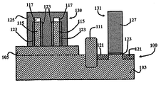
본 발명의 실시예에 따른 집적 회로 장치(100)의 형성은, 도 1 내지 도 8에서 도시되는 일반적으로 순차적인 제조 단계를 통해 도시된다. 일반적으로 완성되는 장치의 대안적인 실시예는 도 9 내지 도 11에서 도시되고, 일반적인 방법 흐름의 예가 도 12 내지 도 14에서 도시된다. 도 1에서 보이는 바와 같이, SOI 웨이퍼(101)는 SIMOX(separation by implantation of oxygen) 또는 웨이퍼 본딩(wafer bonding) 및 에치백(etch-back)에 의한 분리, 또는 해당 분야에서 일반적으로 사용되는 다른 주지 기술과 같은 주지 기술들을 사용하여 형성된다. SOI 웨이퍼(101)는 기판(103) 상부의 매립된 분리층(105) 상부의 실리콘층(115)를 포함한다. 매립된 분리층(105)은 절연 물질을 포함하나, 매립된 산화물을 제외한 임의 유형의 매립된 절연체가 매립된 분리층(105)의 대안으로 사용될 수 있다. 바람직하게는, 매립된 분리층(105)은 매우 얇고, 약 20-2000Å이다.Formation of
일 실시예에서, 기판(103)은 단결정(single crystal) 실리콘층을 포함한다. 대안적으로, 기판(103)은 실리콘(Si), 게르마늄(Ge), 인화갈륨(GaP), 비소화인듐(InAs), 인화인듐(InP), 실리콘 게르마늄(SiGe), 비소화갈륨(GaAs), 또는 다른 Ⅲ/Ⅴ족 화합물을 포함하는(그러나 이들에 한정되지는 않음) 임의의 적당한 반도체 물질을 포함할 수 있다. 기판(103)의 반전을 방지하기 위해, 기판(103)의 일부는 약하게 도핑된 리트로그레이드웰 영역(104,106)을 포함한다. 추가적으로, 강하게 도핑된 리트로그레이드웰 영역(108,110)이 기판(103) 내에 역시 형성된다. 당업자는 웰 영역(104,106,108,110)이, 대응하는 엔웰(Nwell) 및/또는 피웰(Pwell) 영역으로서 구체화될 수 있다. 또한, 리트로그레이드웰 영역(104,106,108,110)은 고에너지 이온 주입 및 어닐링(annealing)과 같은 임의의 주지 기술을 사용하여 형성될 수 있다. 더욱이, 당업자는 리트로그레이드웰 영역(104,106,108,110)이 이후의 프로세싱 단계에 남아 있음을 이해할 수 있을 것이나, 본 발명의 실시예에 의해 제공되는 다른 적절한 피처를 불명확하게 하지 않도록 하기 위해, 리트로그레이드웰 영역(104,106,108,110)은 도 2 내지 도 11의 도면에 도시된 구조체 내에도 존재하지만 상기 도면들 내에서 생략되어 있다. 약하게 도핑된 웰의 통상의 도즈(dose)는 약 1×10¹⁴ 내지 5×10¹⁵/㎤ 이고, 강하게 도핑된 웰의 도즈는 약 3×10¹⁷ 내지 8×10¹⁸/㎤ 이다. 도 2에서 보이는 바와 같이, 하드마스크 필름(hardmask film)(107)은 실리콘층(115) 상부에 증착된다. 그 후, 하드마스크 필름(107), 실리콘층(115), 매립된 분리층(105) 및 하부 기판(103)이 에칭에 의해 제거되는 곳에서 적합한 지향성 에칭이 수행되고, 그로 인해 장치(100)에 좁은 갭(109)을 형성한다. 다음으로, 도 3은 유전층(111)이 갭(109)필링(filling)을 포함해 하드마스크 필름(107) 상부로 증착된 후의 IC 장치(100)를 도시한다. 유전층(111)은, 집적 회로(100) 내의 다양한 장치들 사이를 전기적으로 분리시키기 위해 결국 얕은 트렌치 분리(shallow trench isolation; STI) 영역(111)이 될 부분(도 4에서 보다 구체적으로 도시)을 형성할 것이다. In one embodiment, the
도 4에서 보이는 바와 같이, 하드마스크 필름(107)과 과도 유전층(111)은 적합한 화학 프로세스에 의해 제거되고, 그로 인해 리세스된(recessed) STI 영역(111)을 형성한다. STI 영역(111)은 본 발명의 제1 실시예에 따라 집적 회로(100)에 통합된다. 그러나, 본 발명의 제2 실시예에 따른 집적 회로(102)(도 9 내지 도 11에 도시됨)는 STI 영역 없이 구성될 것이다. 따라서, 본 발명의 제2 실시예의 제조에 있어서, 하드마스크 필름(107)의 증착, 후속되는 에칭 및 유전층(111)의 증착을 포함하는, STI 영역(111)의 형성과 관련된 프로세싱 단계가 포함되지 않는다.As shown in FIG. 4, the
다음으로, 도 5에서 도시된 바와 같이, 유전체 캡층(dielectric cap layer)(117)은 증착되고, 마스킹되고(masked), 에칭된다. 더욱이, 실리콘층(115)은 이 하드마스크 필름(117)을 사용해 에칭된다. 전체적으로, 실리콘층(115)와 유전층(117)은 핀 구조체(113)를 형성한다. 그 후에, 도 6에서 보이는 바와 같이, 레지스트층(119)은 매립된 분리층(105)의 일부를 노출시키고 핀 구조체(113)를 보호하도록 마스킹된다. 필름(119)은 바람직하게는, 매립된 분리층(105)을 에칭할 수 있도록 마스킹되고 노출된 레지스트 이미지(resist image)를 포함한다. 그 후, 필름(119)에 의해 보호되지 않는(즉, 장치(100)의 평면 영역) 매립된 분리층(105)의 일부분들이 제거됨으로써 에칭 프로세스가 일어나고, 그에 의해 하부층(103)을 노출시킨다.Next, as shown in FIG. 5, a
도 7에서 도시된 바와 같이, 필름(119)이 적합한 화학 프로세스에 의해 제거된 후에, 니트라이드(nitride)를 포함할 수 있는 유전 박층(123)(예컨대, 약 10-40Å 두께)이 장치(100) 상에서, 더 명확하게는, 실리콘층(115), 유전층(117), 실리콘 기판(103)의 노출된 모든 부분, 및 소스/드레인 정션(junction)(121)(도 8에서 도시됨) 상부에서 열적으로 성장한다. 실리콘층(115)을 둘러싸는 유전층(123)은 핀 구조체(113)에 대해 게이트 유전체로서 작용하고, 기판(103) 상부의 유전층(123)은 게이트 유전체(123)로 작용한다. As shown in FIG. 7, after the
도 8은, 바람직하게는 폴리실리콘 또는 실리콘 게르마늄 물질을 포함하는 게이트 물질(125,127)이 장치(100) 상부에 증착된 후의 장치(100)의 제1 실시예를 도시한다. 그 후, 장치(100)는 단일 단계에서 게이트 물질(125,127)을 평탄화시키기 위한 화학 기계적 연마(chemical mechanical polishing; CMP) 프로세스를 수행하고, 그에 의해 반복 프로세싱 단계를 제거시켜, FET 게이트(127) 및 FinFET 게이트(125)가 유사한 높이로 구성되도록 한다. 그 후, FET 및 FinFET 게이트(127,125)는 각각, 공지의 리소그래피 기술을 사용해 패턴화되고, 게이트 물질(125,127)의 일부분들이 FinFET 게이트 전극(125) 및 FET 게이트 전극(127)을 형성하기 위해 반응성 이온 에칭(reactive ion etching; RIE) 프로세스로 인해 선택적으로 제거됨으로써 에칭된다. 추가적으로, 에칭 프로세스 중에 유전층(123)의 노출된 영역도 역시 제거된다.FIG. 8 shows a first embodiment of
소스/드레인 임플란트 정션(121)(그들 사이의 채널 영역(도시되지 않음)과 함께)도 역시 기판(103) 내에서 형성된다. 마찬가지로, 소스/드레인 임플란트 정션(122)(그들 사이의 채널 영역(도시되지 않음)과 함께)도 역시, 기판 내에서 소스/드레인 임플란트 정션(121)의 형성과 동시에 FinFET 게이트(125)의 대향하는 측면들 상에 형성된다. 제 1 실시예에서도 비슷한 구성이 제공되어 있지만, 소스/드레인 임플란트 정션(122)은 본 발명의 제2 실시예에 대응하는 도 10 및 도 11에 가장 잘 나타나 있다. 소스/드레인 임플란트 정션(121,122)의 형성은 제조 시퀀스의 임의의 적절한 시점에서 발생할 수 있다. 게다가, 소스/드레인 임플란트 정션(121,122)은 특정 성능의 요구에 의해 만들어진 임의의 공지 방법을 사용해 완성될 수 있다. 그러한 것으로, 다양한 레벨의 복잡도를 가지는 소스/드레인 정션(121,122)을 형성하는 다양한 방법들이 있다. 본 발명의 일부 실시예에서, 소스/드레인 정션(121,122)은 약하게 도핑되고 이온 주입을 사용하여 형성될 수 있다. 예컨대, NFETs의 경우, 소스/드레인 임플란트(121,122)를 위해 보통 인(P), 비소(As), 안티몬(Sb), 또는 다른 적합한 물질이, 1 내지 5 keV의 범위이고 5×10¹⁴ 내지 2×10¹⁵/㎠ 의 도즈에서 사용될 수 있다. 마찬가지로, PFETs의 경우, 소스/드레인 임플란트(121,122)를 위해 보통 붕소(B), 인듐(In), 갈륨(Ga), 또는 다른 적합한 물질이, 0.5 내지 3 keV의 범위이고 5×10¹⁴ 내지 2×10¹⁵/㎠ 의 도즈에서 사용될 수 있다.Source / drain implant junction 121 (along with the channel region (not shown) between them) is also formed in
또한, 본 발명의 다른 실시예에서, 단채널 효과(Short Channel Effect; SCE)를 개선하기 위해서 확장 및 할로(halo) 임플란트(도시되지 않음)가 형성될 수 있다. NFETs의 경우, 할로 임플란트를 위해 보통 붕소(B), 인듐(In), 갈륨(Ga), 또는 다른 적합한 물질이, 5 내지 15 keV의 범위의 에너지이고 1×10¹³내지 8×10¹³/㎠ 의 도즈에서 사용될 수 있다. 마찬가지로, PFETs의 경우, 할로 임플란트를 위해 보통 인(P), 비소(As), 안티몬(Sb), 또는 다른 적합한 물질이, 20 내지 45 keV의 범위이고 1×10¹³ 내지 8×10¹³/㎠ 의 도즈에서 사용될 수 있다. In addition, in other embodiments of the present invention, expansion and halo implants (not shown) may be formed to improve the Short Channel Effect (SCE). For NFETs, boron (B), indium (In), gallium (Ga), or other suitable materials for halo implants are usually in the range of 5 to 15 keV and have energy in the range of 1 × 10 13 to 8 × 10 13 / cm 2. Can be used in the dose. Likewise, for PFETs, phosphorus (P), arsenic (As), antimony (Sb), or other suitable materials for halo implants are usually in the range of 20 to 45 keV and in the range of 1 × 10 13 to 8 × 10 13 / cm 2. Can be used in the dose.
도 9 내지 도 11은 게이트 전극(125) 및 FET 게이트 전극(127)이 형성된 후의 장치(100)의 제2 실시예를 도시한다. 또, 제1 및 제2 실시예의 차이점은 제1 실시예의 장치(100)는 융기형(raised) STI 영역(11)을 포함하는 반면에, 제2 실시예의 장치(102)는 트렌치 분리 영역을 포함하지 않는다는 점이다. 게이트 물질(125,127)은 평면 영역(131)(매립된 분리층(105)이 제거되는 영역) 및 FINFET 영역(130) 상에 증착되고, 단일 에칭으로 양쪽 영역에서 에칭된다. 따라서, 본 발명의 실시예에 의해서 제공되는 제조 기술은 일반 SOI FINFET 프로세스에 단지 약간의 변형만을 요구하고, FET 구조체(131) 및 FinFET 구조체(130)에서 무시할 수 있는 게이트 단차 차이를 가진 제조 프로세스를 용이하도록 해준다. 도 10 및 도 11은 제2 실시예를 명확히 도시하고 있지만, 당업자는 도 10 및 도 11이 제1 실시예에서 제공되는 STI 영역(111)을 포함하지 않는 것을 제외하고, 제1 실시예의 대안적인 뷰를 제공함을 쉽게 이해할 수 있을 것이다. 더욱이, 도 11에서 AA-AA' 파선은 도 9의 단면도의 경계를 제공한다. 9-11 show a second embodiment of the
FET 구조체(131) 및 FinFET 구조체(130)의 형성 후에, 장치(100,102)는 장치높이 위에서 형성되는 인터커넥트(interconnect), 콘택(contact), 배선층(wiring layer) 등(도시되지 않음)을 포함하는 남아있는 집적 회로 구조체의 형성을 위한 종래 프로세스를 수행한다. 더욱이, 다수의 다마신층(damascene layer)(도시되지 않음)은 종래 제조 기술에 따라 장치(100,102) 상부에 형성될 수 있다.After formation of the
도 1 내지 도 11에 도시되는 구조체는, 장치를 기판(103) 내에 배치할지, 종래 접근 방식과 반대되도록, 매립된 분리층(105) 상부의 영역에 배치할지 선택함으로써 민감한 장치의 향상된 열제어를 달성할 수 있다. 게다가, 아날로그 및 ESD 장치가 이 향상된 열제어에 이익이 된다. 기판(103)에 장착된 장치는 역시 향상된 파워 관리(power management)를 위한 기판 바이어싱을 지지할 수 있다. 또한, 도 1 내지 도 11에 도시된 구조체의 프로세스는 상당히 덜 복잡하고, 종래 장치 및 프로세스에 비해 훌륭한 열제어를 제공하면서도 절감된 비용에서 수행될 수 있다.The structures shown in FIGS. 1-11 provide improved thermal control of sensitive devices by selecting whether to place the device within the
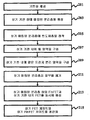
본 발명의 다른 실시예는 도 12 내지 도 14의 흐름도에 도시되어 있으며, 상기 도면들은, 도 12가 집적 회로(100)를 형성하는 방법으로서, 기판(103)을 제공하는 단계(201); 상기 기판 상부에 매립된 분리층(105)을 형성하는 단계(203); 및 상기 매립된 분리층(105)에 반도체층(115)을 접착하는 단계(205)를 포함하는 방법을 도시함으로써, 도 1 내지 도 11에 도시되는 컴포넌트를 언급하는 설명을 포함한다. 상기 방법의 다음 단계는 기판(103) 내의 웰 영역(104,106,108,110)을 구성하는 단계(207), 선택적으로 기판(103) 내의 STI 영역(111)을 구성하는 단계(209), 매립된 분리층(105)의 일부를 제거하는 단계(211), 및 매립된 분리층(105) 상부의 FinFET(130) 및 기판(103) 내의 FET(131)을 동시에 형성하는 단계를 포함한다. 그 후에, 상기 방법은 FET 게이트(127) 및 FinFET 게이트(125)를 평탄화하는 단계(215)를 포함한다. 일 실시예에서, 상기 매립된 절연층(105)은 매립된 산화물로 형성된다. Another embodiment of the present invention is shown in the flow charts of FIGS. 12-14, wherein the method of FIG. 12 forms an
도 13의 흐름도에 보이는 바와 같이, FinFET(130)을 형성하는 단계(213)의 프로세스는 반도체층(115) 상부에 제1 FinFET 유전층(117)을 형성하는 단계(223), 매립된 분리층(105) 상부의, 측벽들을 포함하는 상기 반도체층(115)을 에칭하는 단계(225); 상기 매립된 분리층의 일부를 선택적으로 제거하는 단계(227), 상기 반도체층(115)의 각각의 측벽을 따라 기판 상부에 제2 FinFET 유전층(123)을 구성하는 단계(229), 상기 제1 및 제2 유전층(117,123) 상부에 FinFET 게이트 영역(125)을 형성하는 단계(231); 그리고 상기 FinFET 게이트 영역(125)의 대향하는 측면들 상에 FinFET 소스/드레인 영역(122)을 형성하는 단계(233)를 포함한다. As shown in the flow chart of FIG. 13, the process of forming
도 14의 흐름도에 보이는 바와 같이, FET(131)을 형성하는 단계(213)(FinFET(130)의 형성과 동시에 발생)의 프로세스는 기판(103) 상부에 FET 게이트 유전층(123)을 형성하는 단계(241); 상기 FET 게이트 유전층(123) 상부에 FET 게이트 영역(127)을 형성하는 단계(243)로서 상기 FET 게이트 유전층(123)은 상기 FET 게이트 영역(127)에 인접한 것인 단계; 그리고 상기 기판(103) 내에 FET 소스/드레인 영역(121)을 형성하는 단계(245)를 포함한다. 또한, 상기 FET 게이트 유전층(123)은 상기 FET 게이트 영역(127)과 상기 기판(103) 사이에 형성된다. 추가적으로, 상기 각각의 FinFET 게이트 영역(125) 및 FET 게이트 영역(127)은 폴리실리콘을 포함한다.As shown in the flowchart of FIG. 14, the process of forming 213 131 (which occurs concurrently with the formation of FinFET 130) involves forming a FET
FinFET SOI 장치(130)를 구비한 기판(103) 내의 평면 IC 장치(131)를 집적화하는 것은 로직 게이트, 메모리 셀, 아날로그 회로, ESD 장치, 캐패시터, 레지스터 등을 포함하는 다양한 유형의 IC 장치를 생산하는 데 사용될 수 있다. 본 발명의 실시예에 의해 제공되는 다른 이점은 평면 장치로서(131) 기판(103) 내에 장착함으로써 키(key) 장치의 열제어 능력이다.Integrating
일반적으로, 본 발명의 실시예는, 기판(103), 상기 기판(103) 상부의 매립된 분리층(105), 상기 매립된 분리층(105) 상부의 FinFET(130), 및 상기 기판(103) 내에 집적화된 FET(131)를 포함하는 구조체(100,102)를 제공하며, 상기 FET 게이트(127)는 상기 FinFET 게이트(125)에 대해 평탄하다. 본 발명의 실시예는, 평면 로직 집적 회로 장치(130)가 FinFET 장치(131)와 통합되고, FET 게이트(127) 및 FinFET 게이트(125)가 단일 제조 단계에서 형성되도록 형성됨으로써, 집적 기술을 용이하게 구현하도록 한다. 예컨대, FET 게이트 물질(127) 및 FinFET 게이트 물질(125)의 증착은 동시에 발생하고, FET 게이트 물질(127) 및 FinFET 게이트 물질(125)의 평탄화도 동시에 발생한다. FET 게이트(127) 및 FinFET 게이트(125)는 동일한 상부 높이로 평탄화되어 추가적인 리소그래피 및 에칭 프로세스가 불필요하게 되고, 그로 인해 제조 단계의 개수가 감소함에 따라 전체 제조 비용이 감소하게 된다.In general, embodiments of the present invention include a
특정 실시예의 상기 설명은, 다른 사람들이 공지의 지식을 적용하여 일반 개념을 벗어나지 않는 특정 실시예를 다양한 적용을 위해 용이하게 변경하고 개조할 수 있는 본 발명의 일반적인 본질을 완전히 보여줄 것이고, 따라서, 그러한 개조 및 변경은 개시된 실시예의 등가물의 의미 및 범위 내에서 이해되도록 의도된다. 본원에서 사용되는 표현이나 용어들은 설명을 위한 것이지 제한하기 위한 것이 아님은 당연하다. 따라서, 본 발명의 실시예가 바람직한 실시예와 관련하여 기술되었더라도, 당업자는 본 발명의 실시예가 첨부된 청구범위의 사상 및 범주 내에서 변형되어 실시될 수 있음을 인식할 것이다.The above description of specific embodiments will fully illustrate the general nature of the invention in which other embodiments can readily be modified and modified for various applications without departing from the general concept by applying known knowledge, and thus Modifications and variations are intended to be understood within the meaning and scope of equivalents of the disclosed embodiments. It is to be understood that the phraseology or terminology used herein is for the purpose of description and not of limitation. Thus, although embodiments of the invention have been described in connection with preferred embodiments, those skilled in the art will recognize that embodiments of the invention may be practiced with modification within the spirit and scope of the appended claims.
Claims (7)
기판;
상기 기판 상부의 매립된 분리층(isolation layer);
상기 매립된 분리층 상부의 핀 전계 효과 트랜지스터(FinFET); 및
상기 기판 내의 전계 효과 트랜지스터(FET)를 포함하고,
상기 FET의 게이트 영역의 상부 표면은 상기 FinFET의 게이트 영역의 상부 표면에 대해 평탄한 것인 평면 기판 장치.A planar substrate device integrated with a fin field effect transistor (FinFET),
Board;
A buried isolation layer over the substrate;
A fin field effect transistor (FinFET) over the buried isolation layer; And
A field effect transistor (FET) in the substrate,
And the top surface of the gate region of the FET is flat to the top surface of the gate region of the FinFET.
측벽들을 포함하는 반도체층;
상기 반도체층 상부의 제1 유전층;
상기 반도체층의 상기 각각의 측벽을 따라 있는 제2 유전층;
상기 제1 및 제2 유전층 상부의 상기 FinFET 게이트 영역; 및
상기 FinFET 게이트 영역의 대향하는 측면들 상의 FinFET 소스/드레인 영역을 포함하는 것인 평면 기판 장치.The method of claim 1, wherein the FinFET,
A semiconductor layer comprising sidewalls;
A first dielectric layer over the semiconductor layer;
A second dielectric layer along each of the sidewalls of the semiconductor layer;
The FinFET gate region over the first and second dielectric layers; And
A FinFET source / drain region on opposing sides of the FinFET gate region.
상기 FET 게이트 영역의 대향하는 측면들 상의 FET 소스/드레인 영역; 및
상기 FET 게이트 영역과 상기 기판 사이의 게이트 유전층을 포함하는 것인 평면 기판 장치.The method of claim 1, wherein the FET,
FET source / drain regions on opposing sides of the FET gate region; And
And a gate dielectric layer between said FET gate region and said substrate.
기판, 이 기판 상부의 매립된 절연층, 및 이 매립된 절연층 상부의 반도체층을 포함하는 절연체 상 실리콘(SOI) 웨이퍼;
상기 매립된 절연층 상부의 핀 전계 효과 트랜지스터(FinFET); 및
상기 기판 내에 집적화된 전계 효과 트랜지스터(FET)를 포함하고,
상기 FET의 게이트 영역의 상부 표면은 상기 FinFET의 게이트 영역의 상부 표면에 대해 평탄한 것인 평면 기판 장치.A planar substrate device integrated with a fin field effect transistor (FinFET),
An on-insulator silicon (SOI) wafer comprising a substrate, a buried insulating layer over the substrate, and a semiconductor layer over the buried insulating layer;
A fin field effect transistor (FinFET) on the buried insulating layer; And
A field effect transistor (FET) integrated in the substrate,
And the top surface of the gate region of the FET is flat to the top surface of the gate region of the FinFET.
상기 반도체층 상의 측벽들;
상기 반도체층 상부의 제1 FinFET 유전층;
상기 반도체층의 상기 각각의 측벽을 따라 있는 제2 FinFET 유전층;
상기 제1 및 제2 FinFET 유전층 상부의 상기 FinFET 게이트 영역; 및
상기 FinFET 게이트 영역의 대향하는 측면들 상의 FinFET 소스/드레인 영역을 포함하는 것인 평면 기판 장치.The method of claim 5, wherein the FinFET,
Sidewalls on the semiconductor layer;
A first FinFET dielectric layer over the semiconductor layer;
A second FinFET dielectric layer along each of the sidewalls of the semiconductor layer;
The FinFET gate region over the first and second FinFET dielectric layers; And
A FinFET source / drain region on opposing sides of the FinFET gate region.
상기 FET 게이트 영역의 대향하는 측면들 상의 FET 소스/드레인 영역; 및
상기 FET 게이트 영역과 상기 기판 사이의 게이트 유전층을 포함하는 것인 평면 기판 장치.The method of claim 5, wherein the FET,
FET source / drain regions on opposing sides of the FET gate region; And
And a gate dielectric layer between said FET gate region and said substrate.
Applications Claiming Priority (2)
| Application Number | Priority Date | Filing Date | Title |
|---|---|---|---|
| US10/711,974 | 2004-10-18 | ||
| US10/711,974 US6949768B1 (en) | 2004-10-18 | 2004-10-18 | Planar substrate devices integrated with finfets and method of manufacture |
Related Parent Applications (1)
| Application Number | Title | Priority Date | Filing Date |
|---|---|---|---|
| KR1020077008883A Division KR100985639B1 (en) | 2004-10-18 | 2005-10-11 | Planar substrate devices integrated with finfets and method of manufacture |
Publications (1)
| Publication Number | Publication Date |
|---|---|
| KR20100105779A true KR20100105779A (en) | 2010-09-29 |
Family
ID=34992630
Family Applications (2)
| Application Number | Title | Priority Date | Filing Date |
|---|---|---|---|
| KR1020077008883A KR100985639B1 (en) | 2004-10-18 | 2005-10-11 | Planar substrate devices integrated with finfets and method of manufacture |
| KR1020107018457A KR20100105779A (en) | 2004-10-18 | 2005-10-11 | Planar substrate devices integrated with finfets and method of manufacture |
Family Applications Before (1)
| Application Number | Title | Priority Date | Filing Date |
|---|---|---|---|
| KR1020077008883A KR100985639B1 (en) | 2004-10-18 | 2005-10-11 | Planar substrate devices integrated with finfets and method of manufacture |
Country Status (7)
| Country | Link |
|---|---|
| US (2) | US6949768B1 (en) |
| EP (1) | EP1805795A4 (en) |
| JP (1) | JP4711446B2 (en) |
| KR (2) | KR100985639B1 (en) |
| CN (1) | CN100533758C (en) |
| TW (1) | TWI380343B (en) |
| WO (1) | WO2006044349A2 (en) |
Cited By (1)
| Publication number | Priority date | Publication date | Assignee | Title |
|---|---|---|---|---|
| KR20170112912A (en) * | 2016-03-25 | 2017-10-12 | 타이완 세미콘덕터 매뉴팩쳐링 컴퍼니 리미티드 | Method for semiconductor device fabrication with improved source drain epitaxy |
Families Citing this family (97)
| Publication number | Priority date | Publication date | Assignee | Title |
|---|---|---|---|---|
| WO2006006438A1 (en) * | 2004-07-12 | 2006-01-19 | Nec Corporation | Semiconductor device and manufacturing method thereof |
| JP2006049627A (en) * | 2004-08-05 | 2006-02-16 | Toshiba Corp | Semiconductor device and its manufacturing method |
| KR100612419B1 (en) * | 2004-10-19 | 2006-08-16 | 삼성전자주식회사 | Semiconductor devices having a fin transistor and a plannar transistor and methods of forming the same |
| JP2006261188A (en) * | 2005-03-15 | 2006-09-28 | Seiko Epson Corp | Semiconductor device and its manufacturing method |
| US7920544B2 (en) * | 2005-03-28 | 2011-04-05 | Qualcomm Incorporated | Method and apparatus for enhancing signal-to-noise ratio of position location measurements |
| JP2007018588A (en) * | 2005-07-06 | 2007-01-25 | Toshiba Corp | Semiconductor storage device and method of driving the semiconductor storage device |
| WO2007049170A1 (en) * | 2005-10-25 | 2007-05-03 | Nxp B.V. | Finfet transistors |
| US7512017B2 (en) * | 2005-12-21 | 2009-03-31 | Intel Corporation | Integration of planar and tri-gate devices on the same substrate |
| US7264743B2 (en) * | 2006-01-23 | 2007-09-04 | Lam Research Corporation | Fin structure formation |
| JP2007294857A (en) * | 2006-03-28 | 2007-11-08 | Elpida Memory Inc | Semiconductor device and manufacturing method therefor |
| US7803670B2 (en) * | 2006-07-20 | 2010-09-28 | Freescale Semiconductor, Inc. | Twisted dual-substrate orientation (DSO) substrates |
| US7456471B2 (en) * | 2006-09-15 | 2008-11-25 | International Business Machines Corporation | Field effect transistor with raised source/drain fin straps |
| US8368144B2 (en) * | 2006-12-18 | 2013-02-05 | Infineon Technologies Ag | Isolated multigate FET circuit blocks with different ground potentials |
| US8492796B2 (en) * | 2007-03-13 | 2013-07-23 | Infineon Technologies Ag | MuGFET switch |
| US7923337B2 (en) * | 2007-06-20 | 2011-04-12 | International Business Machines Corporation | Fin field effect transistor devices with self-aligned source and drain regions |
| JP4459257B2 (en) * | 2007-06-27 | 2010-04-28 | 株式会社東芝 | Semiconductor device |
| US9064963B2 (en) * | 2007-09-28 | 2015-06-23 | Infineon Technologies Ag | Semiconductor structure |
| US8329564B2 (en) * | 2007-10-26 | 2012-12-11 | International Business Machines Corporation | Method for fabricating super-steep retrograde well MOSFET on SOI or bulk silicon substrate, and device fabricated in accordance with the method |
| US7786535B2 (en) * | 2008-01-11 | 2010-08-31 | International Business Machines Corporation | Design structures for high-voltage integrated circuits |
| US7790543B2 (en) * | 2008-01-11 | 2010-09-07 | International Business Machines Corporation | Device structures for a metal-oxide-semiconductor field effect transistor and methods of fabricating such device structures |
| US7790524B2 (en) * | 2008-01-11 | 2010-09-07 | International Business Machines Corporation | Device and design structures for memory cells in a non-volatile random access memory and methods of fabricating such device structures |
| US7772651B2 (en) * | 2008-01-11 | 2010-08-10 | International Business Machines Corporation | Semiconductor-on-insulator high-voltage device structures, methods of fabricating such device structures, and design structures for high-voltage circuits |
| WO2009110048A1 (en) * | 2008-02-15 | 2009-09-11 | 日本ユニサンティスエレクトロニクス株式会社 | Semiconductor devuce and manufacturing method thereof |
| US8211786B2 (en) * | 2008-02-28 | 2012-07-03 | International Business Machines Corporation | CMOS structure including non-planar hybrid orientation substrate with planar gate electrodes and method for fabrication |
| US8331068B2 (en) | 2009-02-19 | 2012-12-11 | Taiwan Semiconductor Manufacturing Company, Ltd. | ESD protection for FinFETs |
| US8305829B2 (en) * | 2009-02-23 | 2012-11-06 | Taiwan Semiconductor Manufacturing Company, Ltd. | Memory power gating circuit for controlling internal voltage of a memory array, system and method for controlling the same |
| US8305790B2 (en) * | 2009-03-16 | 2012-11-06 | Taiwan Semiconductor Manufacturing Company, Ltd. | Electrical anti-fuse and related applications |
| US8957482B2 (en) * | 2009-03-31 | 2015-02-17 | Taiwan Semiconductor Manufacturing Company, Ltd. | Electrical fuse and related applications |
| US8912602B2 (en) * | 2009-04-14 | 2014-12-16 | Taiwan Semiconductor Manufacturing Company, Ltd. | FinFETs and methods for forming the same |
| US7968971B2 (en) * | 2009-06-22 | 2011-06-28 | Taiwan Semiconductor Manufacturing Co., Ltd. | Thin-body bipolar device |
| US8461015B2 (en) * | 2009-07-08 | 2013-06-11 | Taiwan Semiconductor Manufacturing Company, Ltd. | STI structure and method of forming bottom void in same |
| US8759943B2 (en) | 2010-10-08 | 2014-06-24 | Taiwan Semiconductor Manufacturing Company, Ltd. | Transistor having notched fin structure and method of making the same |
| US8980719B2 (en) | 2010-04-28 | 2015-03-17 | Taiwan Semiconductor Manufacturing Company, Ltd. | Methods for doping fin field-effect transistors |
| US8623728B2 (en) * | 2009-07-28 | 2014-01-07 | Taiwan Semiconductor Manufacturing Company, Ltd. | Method for forming high germanium concentration SiGe stressor |
| US8497528B2 (en) | 2010-05-06 | 2013-07-30 | Taiwan Semiconductor Manufacturing Company, Ltd. | Method for fabricating a strained structure |
| US8629478B2 (en) * | 2009-07-31 | 2014-01-14 | Taiwan Semiconductor Manufacturing Company, Ltd. | Fin structure for high mobility multiple-gate transistor |
| US8482073B2 (en) * | 2010-03-25 | 2013-07-09 | Taiwan Semiconductor Manufacturing Company, Ltd. | Integrated circuit including FINFETs and methods for forming the same |
| US8298925B2 (en) | 2010-11-08 | 2012-10-30 | Taiwan Semiconductor Manufacturing Company, Ltd. | Mechanisms for forming ultra shallow junction |
| US8472227B2 (en) * | 2010-01-27 | 2013-06-25 | Taiwan Semiconductor Manufacturing Company, Ltd. | Integrated circuits and methods for forming the same |
| US9484462B2 (en) | 2009-09-24 | 2016-11-01 | Taiwan Semiconductor Manufacturing Company, Ltd. | Fin structure of fin field effect transistor |
| US8440517B2 (en) | 2010-10-13 | 2013-05-14 | Taiwan Semiconductor Manufacturing Company, Ltd. | FinFET and method of fabricating the same |
| US9112052B2 (en) | 2009-10-14 | 2015-08-18 | Taiwan Semiconductor Manufacturing Company, Ltd. | Voids in STI regions for forming bulk FinFETs |
| US8519481B2 (en) | 2009-10-14 | 2013-08-27 | Taiwan Semiconductor Manufacturing Company, Ltd. | Voids in STI regions for forming bulk FinFETs |
| US20110097867A1 (en) * | 2009-10-22 | 2011-04-28 | Taiwan Semiconductor Manufacturing Company, Ltd. | Method of controlling gate thicknesses in forming fusi gates |
| US8436404B2 (en) | 2009-12-30 | 2013-05-07 | Intel Corporation | Self-aligned contacts |
| US9040393B2 (en) | 2010-01-14 | 2015-05-26 | Taiwan Semiconductor Manufacturing Company, Ltd. | Method of forming semiconductor structure |
| US8513723B2 (en) * | 2010-01-19 | 2013-08-20 | International Business Machines Corporation | Method and structure for forming high performance MOS capacitor along with fully depleted semiconductor on insulator devices on the same chip |
| CN102315268B (en) * | 2010-07-01 | 2013-07-10 | 中国科学院微电子研究所 | Semiconductor device and making method thereof |
| US8354319B2 (en) | 2010-10-15 | 2013-01-15 | International Business Machines Corporation | Integrated planar and multiple gate FETs |
| US8603924B2 (en) | 2010-10-19 | 2013-12-10 | Taiwan Semiconductor Manufacturing Company, Ltd. | Methods of forming gate dielectric material |
| US8769446B2 (en) | 2010-11-12 | 2014-07-01 | Taiwan Semiconductor Manufacturing Company, Ltd. | Method and device for increasing fin device density for unaligned fins |
| US8877602B2 (en) | 2011-01-25 | 2014-11-04 | Taiwan Semiconductor Manufacturing Company, Ltd. | Mechanisms of doping oxide for forming shallow trench isolation |
| US8592915B2 (en) | 2011-01-25 | 2013-11-26 | Taiwan Semiconductor Manufacturing Company, Ltd. | Doped oxide for shallow trench isolation (STI) |
| CN102651321B (en) * | 2011-02-25 | 2015-03-04 | 中国科学院微电子研究所 | Manufacturing method for semiconductor devices |
| US8431453B2 (en) | 2011-03-31 | 2013-04-30 | Taiwan Semiconductor Manufacturing Company, Ltd. | Plasma doping to reduce dielectric loss during removal of dummy layers in a gate structure |
| CN102842508B (en) * | 2011-06-24 | 2015-03-04 | 中国科学院微电子研究所 | Manufacturing method for semiconductor field effect transistor |
| US8778744B2 (en) * | 2011-06-24 | 2014-07-15 | Institute of Microelectronics, Chinese Academy of Sciences | Method for manufacturing semiconductor field effect transistor |
| CN102842507B (en) * | 2011-06-24 | 2015-08-19 | 中国科学院微电子研究所 | The preparation method of semiconductor field effect transistor |
| US8842945B2 (en) * | 2011-08-09 | 2014-09-23 | Soitec | Methods of forming three dimensionally integrated semiconductor systems including photoactive devices and semiconductor-on-insulator substrates |
| CN103022038B (en) * | 2011-09-21 | 2015-06-10 | 中国科学院微电子研究所 | Static random access memory (SRAM) unit and manufacturing method thereof |
| US9397104B2 (en) | 2011-09-21 | 2016-07-19 | Institute of Microelectronics, Chinese Academy of Sciences | SRAM cell and method for manufacturing the same |
| WO2013095550A1 (en) | 2011-12-22 | 2013-06-27 | Intel Corporation | Semiconductor device having a necked semiconductor body and method of forming semiconductor bodies of varying width |
| US20130173214A1 (en) * | 2012-01-04 | 2013-07-04 | International Business Machines Corporation | Method and structure for inline electrical fin critical dimension measurement |
| US8587068B2 (en) | 2012-01-26 | 2013-11-19 | International Business Machines Corporation | SRAM with hybrid FinFET and planar transistors |
| US8466012B1 (en) * | 2012-02-01 | 2013-06-18 | International Business Machines Corporation | Bulk FinFET and SOI FinFET hybrid technology |
| US8692291B2 (en) | 2012-03-27 | 2014-04-08 | International Business Machines Corporation | Passive devices for FinFET integrated circuit technologies |
| US9219056B2 (en) | 2012-03-27 | 2015-12-22 | International Business Machines Corporation | Passive devices for FinFET integrated circuit technologies |
| US8916426B2 (en) | 2012-03-27 | 2014-12-23 | International Business Machines Corporation | Passive devices for FinFET integrated circuit technologies |
| US9583398B2 (en) * | 2012-06-29 | 2017-02-28 | Taiwan Semiconductor Manufacturing Company, Ltd. | Integrated circuit having FinFETS with different fin profiles |
| US8586449B1 (en) | 2012-08-14 | 2013-11-19 | International Business Machines Corporation | Raised isolation structure self-aligned to fin structures |
| US8987823B2 (en) * | 2012-11-07 | 2015-03-24 | International Business Machines Corporation | Method and structure for forming a localized SOI finFET |
| US8759874B1 (en) * | 2012-11-30 | 2014-06-24 | Stmicroelectronics, Inc. | FinFET device with isolated channel |
| US8890249B2 (en) | 2012-11-30 | 2014-11-18 | International Business Machines Corporation | Bulk FinFET ESD device |
| US9054124B2 (en) | 2012-12-14 | 2015-06-09 | International Business Machines Corporation | Electrostatic discharge resistant diodes |
| FR3005309B1 (en) | 2013-05-02 | 2016-03-11 | Commissariat Energie Atomique | NANOWELL AND PLANNER TRANSISTORS COINTEGRATED ON SUBSTRATE SOI UTBOX |
| US8963259B2 (en) * | 2013-05-31 | 2015-02-24 | Globalfoundries Inc. | Device isolation in finFET CMOS |
| US8957478B2 (en) * | 2013-06-24 | 2015-02-17 | International Business Machines Corporation | Semiconductor device including source/drain formed on bulk and gate channel formed on oxide layer |
| US9515184B2 (en) * | 2013-09-12 | 2016-12-06 | Taiwan Semiconductor Manufacturing Company Limited | Semiconductor arrangement with multiple-height fins and substrate trenches |
| US9048123B2 (en) | 2013-09-19 | 2015-06-02 | International Business Machines Corporation | Interdigitated finFETs |
| US9312272B2 (en) | 2013-11-27 | 2016-04-12 | Globalfoundries Inc. | Implementing buried FET utilizing drain of finFET as gate of buried FET |
| US9059020B1 (en) | 2013-12-02 | 2015-06-16 | International Business Machins Corporation | Implementing buried FET below and beside FinFET on bulk substrate |
| US9099570B2 (en) * | 2013-12-05 | 2015-08-04 | Stmicroelectronics, Inc. | Method for the formation of dielectric isolated fin structures for use, for example, in FinFET devices |
| US20150171217A1 (en) * | 2013-12-12 | 2015-06-18 | Texas Instruments Incorporated | Design and integration of finfet device |
| US9443851B2 (en) * | 2014-01-03 | 2016-09-13 | Samsung Electronics Co., Ltd. | Semiconductor devices including finFETs and local interconnect layers and methods of fabricating the same |
| US9129863B2 (en) | 2014-02-11 | 2015-09-08 | International Business Machines Corporation | Method to form dual channel group III-V and Si/Ge FINFET CMOS |
| US9123585B1 (en) | 2014-02-11 | 2015-09-01 | International Business Machines Corporation | Method to form group III-V and Si/Ge FINFET on insulator |
| KR102171023B1 (en) * | 2014-07-21 | 2020-10-29 | 삼성전자주식회사 | Method of fabricating semiconductor devices |
| KR102245133B1 (en) | 2014-10-13 | 2021-04-28 | 삼성전자 주식회사 | Semiconductor device comprising finFETs(fin Field Effect Transistors) of different gate structures and method for fabricating the same |
| US9391065B1 (en) | 2015-06-29 | 2016-07-12 | Globalfoundries Inc. | Electrostatic discharge and passive structures integrated in a vertical gate fin-type field effect diode |
| CN108243625B (en) * | 2015-11-03 | 2022-04-22 | 硅存储技术公司 | Split-gate non-volatile flash memory cell with metal gate and method of making the same |
| KR102402771B1 (en) | 2015-12-11 | 2022-05-26 | 삼성전자주식회사 | Semiconductor device and method for fabricating the same |
| US9899378B2 (en) | 2015-12-14 | 2018-02-20 | International Business Machines Corporation | Simultaneously fabricating a high voltage transistor and a finFET |
| EP3182461B1 (en) * | 2015-12-16 | 2022-08-03 | IMEC vzw | Method for fabricating finfet technology with locally higher fin-to-fin pitch |
| US10147802B2 (en) * | 2016-05-20 | 2018-12-04 | Globalfoundries Inc. | FINFET circuit structures with vertically spaced transistors and fabrication methods |
| US10290654B2 (en) | 2016-05-20 | 2019-05-14 | Globalfoundries Inc. | Circuit structures with vertically spaced transistors and fabrication methods |
| US9646962B1 (en) | 2016-10-05 | 2017-05-09 | International Business Machines Corporation | Low leakage gate controlled vertical electrostatic discharge protection device integration with a planar FinFET |
| RU2670248C1 (en) * | 2017-09-05 | 2018-10-19 | Акционерное общество "Научно-исследовательский институт молекулярной электроники" | Method for forming local buried dielectric insulation region of active part of transistors with three-dimensional structure of shell (finfet) |
Family Cites Families (25)
| Publication number | Priority date | Publication date | Assignee | Title |
|---|---|---|---|---|
| JPH04179166A (en) * | 1990-11-09 | 1992-06-25 | Hitachi Ltd | Insulated gate semiconductor device and manufacture thereof |
| JP2789931B2 (en) * | 1991-05-27 | 1998-08-27 | 日本電気株式会社 | Semiconductor device |
| JP3462301B2 (en) * | 1995-06-16 | 2003-11-05 | 三菱電機株式会社 | Semiconductor device and manufacturing method thereof |
| US6140163A (en) * | 1997-07-11 | 2000-10-31 | Advanced Micro Devices, Inc. | Method and apparatus for upper level substrate isolation integrated with bulk silicon |
| KR100562539B1 (en) * | 1997-12-19 | 2006-03-22 | 어드밴스드 마이크로 디바이시즈, 인코포레이티드 | Silicon-on-insulator configuration which is compatible with bulk cmos architecture |
| US6093585A (en) * | 1998-05-08 | 2000-07-25 | Lsi Logic Corporation | High voltage tolerant thin film transistor |
| US6252284B1 (en) | 1999-12-09 | 2001-06-26 | International Business Machines Corporation | Planarized silicon fin device |
| US6607950B2 (en) * | 2000-03-30 | 2003-08-19 | Interuniversitair Microelektronic Centrum (Imec) | MIS transistors with a metal gate and high-k dielectric and method of forming |
| JP2002057220A (en) * | 2000-08-11 | 2002-02-22 | Seiko Epson Corp | Semiconductor device and manufacturing method therefor |
| US6720231B2 (en) | 2002-01-28 | 2004-04-13 | International Business Machines Corporation | Fin-type resistors |
| JP2003229575A (en) * | 2002-02-04 | 2003-08-15 | Hitachi Ltd | Integrated semiconductor device and manufacturing method therefor |
| JP3782021B2 (en) * | 2002-02-22 | 2006-06-07 | 株式会社東芝 | Semiconductor device, semiconductor device manufacturing method, and semiconductor substrate manufacturing method |
| US6995412B2 (en) | 2002-04-12 | 2006-02-07 | International Business Machines Corporation | Integrated circuit with capacitors having a fin structure |
| US7074623B2 (en) * | 2002-06-07 | 2006-07-11 | Amberwave Systems Corporation | Methods of forming strained-semiconductor-on-insulator finFET device structures |
| EP1383166A3 (en) * | 2002-07-16 | 2006-10-11 | Interuniversitair Microelektronica Centrum ( Imec) | FIN field effect transistor device and a method for manufacturing such device |
| US6770516B2 (en) * | 2002-09-05 | 2004-08-03 | Taiwan Semiconductor Manufacturing Company | Method of forming an N channel and P channel FINFET device on the same semiconductor substrate |
| JP4546021B2 (en) * | 2002-10-02 | 2010-09-15 | ルネサスエレクトロニクス株式会社 | Insulated gate field effect transistor and semiconductor device |
| US6670516B1 (en) * | 2002-12-20 | 2003-12-30 | Uop Llc | Process for producing phenyl-alkanes using olefin isomerization and paraffin recycle |
| JP2004214413A (en) * | 2002-12-27 | 2004-07-29 | Toshiba Corp | Semiconductor device |
| CN1762047A (en) * | 2003-03-20 | 2006-04-19 | 松下电器产业株式会社 | Semiconductor device and method for fabricating the same |
| US6844238B2 (en) * | 2003-03-26 | 2005-01-18 | Taiwan Semiconductor Manufacturing Co., Ltd | Multiple-gate transistors with improved gate control |
| US20050003592A1 (en) * | 2003-06-18 | 2005-01-06 | Jones A. Brooke | All-around MOSFET gate and methods of manufacture thereof |
| WO2005022637A1 (en) * | 2003-08-28 | 2005-03-10 | Nec Corporation | Semiconductor device having fin-type field effect transistors |
| US7211864B2 (en) * | 2003-09-15 | 2007-05-01 | Seliskar John J | Fully-depleted castellated gate MOSFET device and method of manufacture thereof |
| WO2006006438A1 (en) * | 2004-07-12 | 2006-01-19 | Nec Corporation | Semiconductor device and manufacturing method thereof |
-
2004
- 2004-10-18 US US10/711,974 patent/US6949768B1/en active Active
-
2005
- 2005-08-09 US US11/200,271 patent/US7368354B2/en active Active
- 2005-10-11 KR KR1020077008883A patent/KR100985639B1/en not_active IP Right Cessation
- 2005-10-11 CN CNB2005800354842A patent/CN100533758C/en active Active
- 2005-10-11 EP EP05809789A patent/EP1805795A4/en not_active Withdrawn
- 2005-10-11 WO PCT/US2005/036471 patent/WO2006044349A2/en active Application Filing
- 2005-10-11 KR KR1020107018457A patent/KR20100105779A/en active IP Right Grant
- 2005-10-11 JP JP2007536791A patent/JP4711446B2/en not_active Expired - Fee Related
- 2005-10-11 TW TW094135386A patent/TWI380343B/en active
Cited By (1)
| Publication number | Priority date | Publication date | Assignee | Title |
|---|---|---|---|---|
| KR20170112912A (en) * | 2016-03-25 | 2017-10-12 | 타이완 세미콘덕터 매뉴팩쳐링 컴퍼니 리미티드 | Method for semiconductor device fabrication with improved source drain epitaxy |
Also Published As
| Publication number | Publication date |
|---|---|
| KR100985639B1 (en) | 2010-10-05 |
| EP1805795A4 (en) | 2010-10-06 |
| JP4711446B2 (en) | 2011-06-29 |
| US6949768B1 (en) | 2005-09-27 |
| JP2008517464A (en) | 2008-05-22 |
| WO2006044349A2 (en) | 2006-04-27 |
| US7368354B2 (en) | 2008-05-06 |
| WO2006044349A9 (en) | 2007-08-16 |
| CN101103463A (en) | 2008-01-09 |
| TW200614334A (en) | 2006-05-01 |
| TWI380343B (en) | 2012-12-21 |
| US20060084212A1 (en) | 2006-04-20 |
| KR20070064346A (en) | 2007-06-20 |
| CN100533758C (en) | 2009-08-26 |
| WO2006044349A3 (en) | 2007-06-07 |
| EP1805795A2 (en) | 2007-07-11 |
Similar Documents
| Publication | Publication Date | Title |
|---|---|---|
| KR100985639B1 (en) | Planar substrate devices integrated with finfets and method of manufacture | |
| US7786535B2 (en) | Design structures for high-voltage integrated circuits | |
| US9196543B2 (en) | Structure and method for finFET device | |
| CN101226941B (en) | Semiconductor device and manufacturing method thereof | |
| US9263449B2 (en) | FinFET and fin-passive devices | |
| US7687862B2 (en) | Semiconductor devices with active regions of different heights | |
| US20100127333A1 (en) | novel layout architecture for performance enhancement | |
| US20080079094A1 (en) | Methods for inducing strain in non-planar transistor structures | |
| US20080248615A1 (en) | Cmos structure for body ties in ultra-thin soi (utsoi) substrates | |
| US7638376B2 (en) | Method for forming SOI device | |
| US20150325692A1 (en) | Fin field effect transistor (finfet) device including a set of merged fins formed adjacent a set of unmerged fins | |
| US20180211879A1 (en) | Stress memorization technique for strain coupling enhancement in bulk finfet device | |
| US9276115B2 (en) | Semiconductor devices and methods of manufacture | |
| CN109119470B (en) | Boundary spacer structure and integration | |
| CN102299177B (en) | Manufacturing method of contact and semiconductor device with contact | |
| TWI414039B (en) | Trench formation in a semiconductor material | |
| US9171952B2 (en) | Low gate-to-drain capacitance fully merged finFET | |
| US8354319B2 (en) | Integrated planar and multiple gate FETs | |
| US20080305613A1 (en) | Method for fabricating an soi defined semiconductor device | |
| US7791105B2 (en) | Device structures for a high voltage junction field effect transistor manufactured using a hybrid orientation technology wafer and design structures for a high voltage integrated circuit | |
| US7772651B2 (en) | Semiconductor-on-insulator high-voltage device structures, methods of fabricating such device structures, and design structures for high-voltage circuits |
Legal Events
| Date | Code | Title | Description |
|---|---|---|---|
| A107 | Divisional application of patent | ||
| A201 | Request for examination | ||
| E902 | Notification of reason for refusal | ||
| E701 | Decision to grant or registration of patent right | ||
| NORF | Unpaid initial registration fee |