JP4711404B2 - 表示装置 - Google Patents
表示装置 Download PDFInfo
- Publication number
- JP4711404B2 JP4711404B2 JP2005234352A JP2005234352A JP4711404B2 JP 4711404 B2 JP4711404 B2 JP 4711404B2 JP 2005234352 A JP2005234352 A JP 2005234352A JP 2005234352 A JP2005234352 A JP 2005234352A JP 4711404 B2 JP4711404 B2 JP 4711404B2
- Authority
- JP
- Japan
- Prior art keywords
- dummy
- pixel
- drain electrode
- electrode line
- tft
- Prior art date
- Legal status (The legal status is an assumption and is not a legal conclusion. Google has not performed a legal analysis and makes no representation as to the accuracy of the status listed.)
- Active
Links
- 239000000758 substrate Substances 0.000 description 59
- 238000010586 diagram Methods 0.000 description 31
- 239000004973 liquid crystal related substance Substances 0.000 description 24
- 230000004048 modification Effects 0.000 description 18
- 238000012986 modification Methods 0.000 description 18
- 239000010410 layer Substances 0.000 description 15
- 238000000034 method Methods 0.000 description 8
- 239000011229 interlayer Substances 0.000 description 4
- 239000004065 semiconductor Substances 0.000 description 4
- 239000000463 material Substances 0.000 description 3
- 239000003566 sealing material Substances 0.000 description 3
- 239000011521 glass Substances 0.000 description 2
- 238000009413 insulation Methods 0.000 description 2
- 239000003990 capacitor Substances 0.000 description 1
- 230000015556 catabolic process Effects 0.000 description 1
- 238000006731 degradation reaction Methods 0.000 description 1
- 230000006866 deterioration Effects 0.000 description 1
- 230000000694 effects Effects 0.000 description 1
- 230000005684 electric field Effects 0.000 description 1
- 239000011159 matrix material Substances 0.000 description 1
- 231100000989 no adverse effect Toxicity 0.000 description 1
Images


Classifications
-
- G—PHYSICS
- G09—EDUCATION; CRYPTOGRAPHY; DISPLAY; ADVERTISING; SEALS
- G09G—ARRANGEMENTS OR CIRCUITS FOR CONTROL OF INDICATING DEVICES USING STATIC MEANS TO PRESENT VARIABLE INFORMATION
- G09G3/00—Control arrangements or circuits, of interest only in connection with visual indicators other than cathode-ray tubes
- G09G3/20—Control arrangements or circuits, of interest only in connection with visual indicators other than cathode-ray tubes for presentation of an assembly of a number of characters, e.g. a page, by composing the assembly by combination of individual elements arranged in a matrix no fixed position being assigned to or needed to be assigned to the individual characters or partial characters
- G09G3/34—Control arrangements or circuits, of interest only in connection with visual indicators other than cathode-ray tubes for presentation of an assembly of a number of characters, e.g. a page, by composing the assembly by combination of individual elements arranged in a matrix no fixed position being assigned to or needed to be assigned to the individual characters or partial characters by control of light from an independent source
- G09G3/36—Control arrangements or circuits, of interest only in connection with visual indicators other than cathode-ray tubes for presentation of an assembly of a number of characters, e.g. a page, by composing the assembly by combination of individual elements arranged in a matrix no fixed position being assigned to or needed to be assigned to the individual characters or partial characters by control of light from an independent source using liquid crystals
- G09G3/3611—Control of matrices with row and column drivers
- G09G3/3614—Control of polarity reversal in general
-
- G—PHYSICS
- G09—EDUCATION; CRYPTOGRAPHY; DISPLAY; ADVERTISING; SEALS
- G09G—ARRANGEMENTS OR CIRCUITS FOR CONTROL OF INDICATING DEVICES USING STATIC MEANS TO PRESENT VARIABLE INFORMATION
- G09G2310/00—Command of the display device
- G09G2310/02—Addressing, scanning or driving the display screen or processing steps related thereto
-
- G—PHYSICS
- G09—EDUCATION; CRYPTOGRAPHY; DISPLAY; ADVERTISING; SEALS
- G09G—ARRANGEMENTS OR CIRCUITS FOR CONTROL OF INDICATING DEVICES USING STATIC MEANS TO PRESENT VARIABLE INFORMATION
- G09G2320/00—Control of display operating conditions
- G09G2320/02—Improving the quality of display appearance
- G09G2320/0247—Flicker reduction other than flicker reduction circuits used for single beam cathode-ray tubes
-
- G—PHYSICS
- G09—EDUCATION; CRYPTOGRAPHY; DISPLAY; ADVERTISING; SEALS
- G09G—ARRANGEMENTS OR CIRCUITS FOR CONTROL OF INDICATING DEVICES USING STATIC MEANS TO PRESENT VARIABLE INFORMATION
- G09G2320/00—Control of display operating conditions
- G09G2320/02—Improving the quality of display appearance
- G09G2320/029—Improving the quality of display appearance by monitoring one or more pixels in the display panel, e.g. by monitoring a fixed reference pixel
-
- G—PHYSICS
- G09—EDUCATION; CRYPTOGRAPHY; DISPLAY; ADVERTISING; SEALS
- G09G—ARRANGEMENTS OR CIRCUITS FOR CONTROL OF INDICATING DEVICES USING STATIC MEANS TO PRESENT VARIABLE INFORMATION
- G09G3/00—Control arrangements or circuits, of interest only in connection with visual indicators other than cathode-ray tubes
- G09G3/20—Control arrangements or circuits, of interest only in connection with visual indicators other than cathode-ray tubes for presentation of an assembly of a number of characters, e.g. a page, by composing the assembly by combination of individual elements arranged in a matrix no fixed position being assigned to or needed to be assigned to the individual characters or partial characters
- G09G3/34—Control arrangements or circuits, of interest only in connection with visual indicators other than cathode-ray tubes for presentation of an assembly of a number of characters, e.g. a page, by composing the assembly by combination of individual elements arranged in a matrix no fixed position being assigned to or needed to be assigned to the individual characters or partial characters by control of light from an independent source
- G09G3/36—Control arrangements or circuits, of interest only in connection with visual indicators other than cathode-ray tubes for presentation of an assembly of a number of characters, e.g. a page, by composing the assembly by combination of individual elements arranged in a matrix no fixed position being assigned to or needed to be assigned to the individual characters or partial characters by control of light from an independent source using liquid crystals
- G09G3/3611—Control of matrices with row and column drivers
- G09G3/3648—Control of matrices with row and column drivers using an active matrix
Description
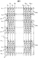
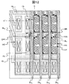
なお、実施例を説明するための全図において、同一機能を有するものは、同一符号を付け、その繰り返しの説明は省略する。
101…ガラス基板
102…第1層間絶縁膜
103…半導体層
104…第2層間絶縁膜
2…CF基板
3…シール材
4…液晶材料
GL…ゲート電極線
DL…ドレイン電極線
CL…共通信号線
PX…画素電極
PXd…ダミーの画素電極
CT…コモン電極
SL…ソース電極
BR…ブリッジ配線
DP1…第1のダミー画素
DP2…第2のダミー画素
DP3…第3のダミー画素
Claims (8)
- TFT素子および画素電極が画素単位で配置された表示パネルを有する表示装置であって、
前記表示パネルは、
有効表示領域内を通る複数のゲート電極線および複数のドレイン電極線を有し、
前記有効表示領域の外側であり、かつ、前記ゲート電極線の延在方向の一方の端部側に位置するドレイン電極線に沿った領域には、前記ドレイン電極線の延在方向の一方の端部側から数えて偶数本目のゲート電極線に接続されたTFT素子を有する第1のダミー画素が配置され、
前記有効表示領域の外側であり、かつ、前記ゲート電極線の延在方向の他方の端部側に位置するドレイン電極線に沿った領域には、前記ドレイン電極線の延在方向の前記一方の端部側から数えて奇数本目のゲート電極線に接続されたTFT素子を有する第2のダミー画素が配置されており、
各ドレイン電極線は、当該ドレイン電極線に接続された各画素のTFT素子が、延在方向に沿って交互に配置されており、
前記ゲート電極線の延在方向の端部に位置する2本の前記ドレイン電極線は、それぞれ、前記有効表示領域内に配置された複数のTFT素子と、複数の前記第1または第2のダミー画素のTFT素子とに接続されており、かつ、前記各ドレイン電極線に接続された前記有効表示領域内のTFT素子と前記第1または第2のダミー画素のTFT素子とは、前記各ドレイン電極線の延在方向に沿って交互に配置されており、
複数の前記第1のダミー画素の間、または複数の前記第2のダミー画素の間には、第3のダミー画素が配置されていることを特徴とする表示装置。 - 前記第1のダミー画素が配置された端部が、前記ゲート電極線の入力端側であることを特徴とする請求項1に記載の表示装置。
- 前記第1および第2のダミー画素は、前記有効表示領域内の画素と同じ構成であることを特徴とする請求項1または請求項2に記載の表示装置。
- 前記第1および第2のダミー画素は、TFT素子のみを有することを特徴とする請求項1または請求項2に記載の表示装置。
- 前記第1または第2のダミー画素の外側に、ダミーのドレイン電極線を有することを特徴とする請求項1に記載の表示装置。
- 前記第3のダミー画素は、前記有効表示領域内の画素の画素電極と同じ導電層に、前記有効表示領域内を通る前記ドレイン電極線とは接続していないダミーの電極層を有することを特徴とする請求項1に記載の表示装置。
- 前記第1または第2のダミー画素の外側にダミーのドレイン電極線を有し、
前記第3のダミー画素は、前記ダミーのドレイン電極線および前記ダミーの電極層と接続されたTFT素子を有することを特徴とする請求項6に記載の表示装置。 - 前記ダミー画素が配置された領域は、遮光されていることを特徴とする請求項1に記載の表示装置。
Priority Applications (4)
| Application Number | Priority Date | Filing Date | Title |
|---|---|---|---|
| JP2005234352A JP4711404B2 (ja) | 2005-08-12 | 2005-08-12 | 表示装置 |
| TW095129648A TW200719065A (en) | 2005-08-12 | 2006-08-11 | Display apparatus |
| US11/502,458 US20070035687A1 (en) | 2005-08-12 | 2006-08-11 | Display device |
| CN2006101157227A CN1912721B (zh) | 2005-08-12 | 2006-08-11 | 显示装置 |
Applications Claiming Priority (1)
| Application Number | Priority Date | Filing Date | Title |
|---|---|---|---|
| JP2005234352A JP4711404B2 (ja) | 2005-08-12 | 2005-08-12 | 表示装置 |
Publications (3)
| Publication Number | Publication Date |
|---|---|
| JP2007047664A JP2007047664A (ja) | 2007-02-22 |
| JP2007047664A5 JP2007047664A5 (ja) | 2007-04-05 |
| JP4711404B2 true JP4711404B2 (ja) | 2011-06-29 |
Family
ID=37721685
Family Applications (1)
| Application Number | Title | Priority Date | Filing Date |
|---|---|---|---|
| JP2005234352A Active JP4711404B2 (ja) | 2005-08-12 | 2005-08-12 | 表示装置 |
Country Status (4)
| Country | Link |
|---|---|
| US (1) | US20070035687A1 (ja) |
| JP (1) | JP4711404B2 (ja) |
| CN (1) | CN1912721B (ja) |
| TW (1) | TW200719065A (ja) |
Cited By (1)
| Publication number | Priority date | Publication date | Assignee | Title |
|---|---|---|---|---|
| US9601075B2 (en) | 2014-01-08 | 2017-03-21 | Samsung Display Co., Ltd. | Display panel, method of manufacturing the display panel and display apparatus |
Families Citing this family (18)
| Publication number | Priority date | Publication date | Assignee | Title |
|---|---|---|---|---|
| JP5199638B2 (ja) * | 2007-10-16 | 2013-05-15 | 株式会社ジャパンディスプレイイースト | 液晶表示装置 |
| KR100937850B1 (ko) * | 2008-04-04 | 2010-01-21 | 엘지디스플레이 주식회사 | 액정 표시 장치 |
| JP5341191B2 (ja) | 2009-07-17 | 2013-11-13 | シャープ株式会社 | 表示装置および表示装置の駆動方法 |
| US20120127148A1 (en) * | 2010-11-24 | 2012-05-24 | Seong-Jun Lee | Display substrate, display panel and display device |
| JP2014026069A (ja) * | 2012-07-26 | 2014-02-06 | Kyocera Display Corp | 液晶表示装置 |
| CN102879965A (zh) * | 2012-10-12 | 2013-01-16 | 京东方科技集团股份有限公司 | 一种液晶显示面板及液晶显示装置 |
| KR102138107B1 (ko) | 2013-10-10 | 2020-07-28 | 삼성디스플레이 주식회사 | 표시 패널의 구동 방법 및 이를 수행하기 위한 표시 장치 |
| KR20160024274A (ko) | 2014-08-25 | 2016-03-04 | 삼성디스플레이 주식회사 | 유기전계발광 표시장치 |
| KR102309455B1 (ko) | 2014-10-13 | 2021-10-08 | 삼성디스플레이 주식회사 | 유기전계발광 표시장치 |
| KR20170007610A (ko) * | 2015-07-09 | 2017-01-19 | 삼성디스플레이 주식회사 | 표시 장치 |
| JP6747068B2 (ja) * | 2016-06-07 | 2020-08-26 | 三菱電機株式会社 | 液晶表示パネルおよび当該液晶表示パネルを備えた液晶表示装置 |
| KR102538750B1 (ko) * | 2016-11-29 | 2023-06-02 | 엘지디스플레이 주식회사 | 액정 표시장치 |
| KR102401648B1 (ko) | 2017-06-07 | 2022-05-26 | 삼성디스플레이 주식회사 | 액정 표시 장치 |
| CN111108432A (zh) * | 2018-02-11 | 2020-05-05 | 华为技术有限公司 | 一种显示屏及终端设备 |
| CN109828397A (zh) * | 2019-04-09 | 2019-05-31 | 惠科股份有限公司 | 像素电路结构 |
| CN111429857A (zh) * | 2020-04-10 | 2020-07-17 | 深圳市华星光电半导体显示技术有限公司 | 一种显示面板的像素驱动电路 |
| EP4138136A4 (en) * | 2020-04-14 | 2023-06-07 | BOE Technology Group Co., Ltd. | DISPLAY SUBSTRATE AND DISPLAY DEVICE |
| CN115547272B (zh) * | 2022-10-28 | 2024-03-15 | 惠科股份有限公司 | 显示面板和显示装置 |
Citations (2)
| Publication number | Priority date | Publication date | Assignee | Title |
|---|---|---|---|---|
| WO2004097786A1 (ja) * | 2003-04-30 | 2004-11-11 | Toshiba Matsushita Display Technology Co., Ltd. | 表示装置用アレイ基板及び表示装置 |
| JP2004341134A (ja) * | 2003-05-14 | 2004-12-02 | Mitsubishi Electric Corp | 画像表示装置 |
Family Cites Families (8)
| Publication number | Priority date | Publication date | Assignee | Title |
|---|---|---|---|---|
| KR100242443B1 (ko) * | 1997-06-16 | 2000-02-01 | 윤종용 | 도트 반전 구동을 위한 액정 패널 및 이를 이용한 액정 표시 장치 |
| KR100587366B1 (ko) * | 2000-08-30 | 2006-06-08 | 엘지.필립스 엘시디 주식회사 | 횡전계방식 액정표시장치 및 그 제조방법 |
| KR100482468B1 (ko) * | 2000-10-10 | 2005-04-14 | 비오이 하이디스 테크놀로지 주식회사 | 프린지 필드 구동 액정 표시 장치 |
| JP4609970B2 (ja) * | 2001-01-17 | 2011-01-12 | カシオ計算機株式会社 | 液晶表示装置 |
| JP4190921B2 (ja) * | 2002-04-10 | 2008-12-03 | シャープ株式会社 | 駆動回路及びそれを備えた表示装置 |
| KR100853772B1 (ko) * | 2002-04-20 | 2008-08-25 | 엘지디스플레이 주식회사 | 액정표시장치의 구동방법 및 장치 |
| JP4589614B2 (ja) * | 2003-10-28 | 2010-12-01 | 株式会社 日立ディスプレイズ | 画像表示装置 |
| TWI387800B (zh) * | 2004-09-10 | 2013-03-01 | Samsung Display Co Ltd | 顯示裝置 |
-
2005
- 2005-08-12 JP JP2005234352A patent/JP4711404B2/ja active Active
-
2006
- 2006-08-11 CN CN2006101157227A patent/CN1912721B/zh active Active
- 2006-08-11 TW TW095129648A patent/TW200719065A/zh not_active IP Right Cessation
- 2006-08-11 US US11/502,458 patent/US20070035687A1/en not_active Abandoned
Patent Citations (2)
| Publication number | Priority date | Publication date | Assignee | Title |
|---|---|---|---|---|
| WO2004097786A1 (ja) * | 2003-04-30 | 2004-11-11 | Toshiba Matsushita Display Technology Co., Ltd. | 表示装置用アレイ基板及び表示装置 |
| JP2004341134A (ja) * | 2003-05-14 | 2004-12-02 | Mitsubishi Electric Corp | 画像表示装置 |
Cited By (1)
| Publication number | Priority date | Publication date | Assignee | Title |
|---|---|---|---|---|
| US9601075B2 (en) | 2014-01-08 | 2017-03-21 | Samsung Display Co., Ltd. | Display panel, method of manufacturing the display panel and display apparatus |
Also Published As
| Publication number | Publication date |
|---|---|
| CN1912721A (zh) | 2007-02-14 |
| CN1912721B (zh) | 2010-08-25 |
| JP2007047664A (ja) | 2007-02-22 |
| US20070035687A1 (en) | 2007-02-15 |
| TWI350421B (ja) | 2011-10-11 |
| TW200719065A (en) | 2007-05-16 |
Similar Documents
| Publication | Publication Date | Title |
|---|---|---|
| JP4711404B2 (ja) | 表示装置 | |
| US20170162160A1 (en) | Liquid crystal display | |
| JP3730161B2 (ja) | 液晶表示装置 | |
| US20200175937A1 (en) | Drive circuit, display device, and drive method | |
| JP4049162B2 (ja) | 電気光学装置及び電子機器 | |
| US20170365227A1 (en) | Display device and driving circuit | |
| US8854291B2 (en) | Gate signal line driving circuit for supressing noise in a gate signal in a display device | |
| JP5128703B2 (ja) | Tft基板及びこれを用いた液晶表示装置 | |
| US20080284708A1 (en) | Liquid Crystal Display Device | |
| JP5199638B2 (ja) | 液晶表示装置 | |
| JP2017040881A (ja) | 駆動回路、表示装置及び駆動方法 | |
| JP4163611B2 (ja) | 液晶表示装置 | |
| JP6906066B2 (ja) | 液晶表示パネル及び装置 | |
| JP2006189477A (ja) | カラー液晶表示装置 | |
| US6917407B2 (en) | Liquid crystal display device and method of fabricating the same | |
| JP6602136B2 (ja) | 表示装置 | |
| KR100894370B1 (ko) | 표시 장치 | |
| JP2006251322A (ja) | 液晶表示装置および電子情報機器 | |
| US8384703B2 (en) | Liquid crystal display device | |
| JP3841074B2 (ja) | 電気光学装置及び電子機器 | |
| JP5398897B2 (ja) | 液晶表示装置 | |
| JP7289693B2 (ja) | 表示装置およびその駆動方法 | |
| JP2011164236A (ja) | 表示装置 | |
| JP4612100B2 (ja) | 液晶表示装置及びこれの製造方法 | |
| JP2008180951A (ja) | 液晶装置及び電子機器 |
Legal Events
| Date | Code | Title | Description |
|---|---|---|---|
| A521 | Request for written amendment filed |
Free format text: JAPANESE INTERMEDIATE CODE: A523 Effective date: 20070215 |
|
| A621 | Written request for application examination |
Free format text: JAPANESE INTERMEDIATE CODE: A621 Effective date: 20080528 |
|
| A977 | Report on retrieval |
Free format text: JAPANESE INTERMEDIATE CODE: A971007 Effective date: 20101021 |
|
| A131 | Notification of reasons for refusal |
Free format text: JAPANESE INTERMEDIATE CODE: A131 Effective date: 20101026 |
|
| A521 | Request for written amendment filed |
Free format text: JAPANESE INTERMEDIATE CODE: A523 Effective date: 20101224 |
|
| A711 | Notification of change in applicant |
Free format text: JAPANESE INTERMEDIATE CODE: A712 Effective date: 20110218 |
|
| RD03 | Notification of appointment of power of attorney |
Free format text: JAPANESE INTERMEDIATE CODE: A7423 Effective date: 20110218 |
|
| TRDD | Decision of grant or rejection written | ||
| A01 | Written decision to grant a patent or to grant a registration (utility model) |
Free format text: JAPANESE INTERMEDIATE CODE: A01 Effective date: 20110315 |
|
| A61 | First payment of annual fees (during grant procedure) |
Free format text: JAPANESE INTERMEDIATE CODE: A61 Effective date: 20110318 |
|
| R150 | Certificate of patent or registration of utility model |
Ref document number: 4711404 Country of ref document: JP Free format text: JAPANESE INTERMEDIATE CODE: R150 |
|
| R250 | Receipt of annual fees |
Free format text: JAPANESE INTERMEDIATE CODE: R250 |
|
| R250 | Receipt of annual fees |
Free format text: JAPANESE INTERMEDIATE CODE: R250 |
|
| R250 | Receipt of annual fees |
Free format text: JAPANESE INTERMEDIATE CODE: R250 |
|
| R250 | Receipt of annual fees |
Free format text: JAPANESE INTERMEDIATE CODE: R250 |
|
| R250 | Receipt of annual fees |
Free format text: JAPANESE INTERMEDIATE CODE: R250 |
|
| R250 | Receipt of annual fees |
Free format text: JAPANESE INTERMEDIATE CODE: R250 |
|
| R250 | Receipt of annual fees |
Free format text: JAPANESE INTERMEDIATE CODE: R250 |
|
| R250 | Receipt of annual fees |
Free format text: JAPANESE INTERMEDIATE CODE: R250 |
|
| S531 | Written request for registration of change of domicile |
Free format text: JAPANESE INTERMEDIATE CODE: R313531 |
|
| S533 | Written request for registration of change of name |
Free format text: JAPANESE INTERMEDIATE CODE: R313533 |
|
| R350 | Written notification of registration of transfer |
Free format text: JAPANESE INTERMEDIATE CODE: R350 |
|
| R250 | Receipt of annual fees |
Free format text: JAPANESE INTERMEDIATE CODE: R250 |
|
| R250 | Receipt of annual fees |
Free format text: JAPANESE INTERMEDIATE CODE: R250 |
|
| S111 | Request for change of ownership or part of ownership |
Free format text: JAPANESE INTERMEDIATE CODE: R313117 |
|
| R350 | Written notification of registration of transfer |
Free format text: JAPANESE INTERMEDIATE CODE: R350 |
|
| R250 | Receipt of annual fees |
Free format text: JAPANESE INTERMEDIATE CODE: R250 |