JP4698996B2 - 半導体装置 - Google Patents
半導体装置 Download PDFInfo
- Publication number
- JP4698996B2 JP4698996B2 JP2004285593A JP2004285593A JP4698996B2 JP 4698996 B2 JP4698996 B2 JP 4698996B2 JP 2004285593 A JP2004285593 A JP 2004285593A JP 2004285593 A JP2004285593 A JP 2004285593A JP 4698996 B2 JP4698996 B2 JP 4698996B2
- Authority
- JP
- Japan
- Prior art keywords
- power supply
- circuit
- circuit block
- clamp
- semiconductor device
- Prior art date
- Legal status (The legal status is an assumption and is not a legal conclusion. Google has not performed a legal analysis and makes no representation as to the accuracy of the status listed.)
- Expired - Fee Related
Links
Images


Classifications
-
- H—ELECTRICITY
- H10—SEMICONDUCTOR DEVICES; ELECTRIC SOLID-STATE DEVICES NOT OTHERWISE PROVIDED FOR
- H10D—INORGANIC ELECTRIC SEMICONDUCTOR DEVICES
- H10D89/00—Aspects of integrated devices not covered by groups H10D84/00 - H10D88/00
- H10D89/60—Integrated devices comprising arrangements for electrical or thermal protection, e.g. protection circuits against electrostatic discharge [ESD]
- H10D89/601—Integrated devices comprising arrangements for electrical or thermal protection, e.g. protection circuits against electrostatic discharge [ESD] for devices having insulated gate electrodes, e.g. for IGFETs or IGBTs
Landscapes
- Semiconductor Integrated Circuits (AREA)
Description
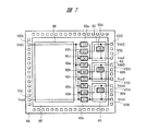
12,96 信号ライン
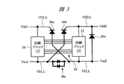
13a〜13d,61a〜61d,62a〜62d,63a〜63d クランプ回路
14a,14b,15a,15b,64a〜64h,92a,93a,94a,95a クランプ回路
20 I/O領域
21 コア領域
30a,30b,30d ダイオード
30c,40c,50c 双方向ダイオード
40a,40b,40d ダイオード接続のMOSトランジスタ
50a,50b,50d GCNMOS回路
51 CMOSインバータ回路
52 NMOSトランジスタ
53 ダイオード
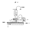
80 半導体デバイス
81 検査板
82 高圧電源
83 抵抗体
84 リレー
90a 信号出力回路
90b,91b 寄生ダイオード
91a 信号入力回路
92〜95 パッド
VD1〜4,VS1〜4 電源端子
VD1_L,VD2_L,VS1_L,VS2_L 電源ライン
R 配線抵抗
R1 抵抗
C コンデンサ
Claims (5)
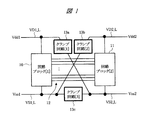
- 第1の電源電圧および第1の基準電圧によって動作する第1の回路ブロックと、第2の電源電圧および第2の基準電圧によって動作する第2の回路ブロックとを備え、前記第1の回路ブロックと前記第2の回路ブロックとの間で信号の送受信が行われる半導体装置であって、
前記第1の電源電圧と前記第2の基準電圧との間をクランプする第1のクランプ回路と、
前記第2の電源電圧と前記第1の基準電圧との間をクランプする第2のクランプ回路と、
前記第1の基準電圧と前記第2の基準電圧との間をクランプする第3のクランプ回路とを有し、
前記第2の回路ブロックは、前記第1の回路ブロックよりも回路面積が小さく、
さらに、前記第2の電源電圧と前記第2の基準電圧との間をクランプする第4のクランプ回路を有することを特徴とする半導体装置。 - 請求項1記載の半導体装置において、
前記第3のクランプ回路は、双方向ダイオードであることを特徴とする半導体装置。 - 請求項1記載の半導体装置において、
前記第1、第2、第4のクランプ回路は、ダイオード接続のMOSトランジスタであることを特徴とする半導体装置。 - 請求項1記載の半導体装置において、
前記第1、第2、第4のクランプ回路は、GCNMOS回路であることを特徴とする半導体装置。 - 第1の電源電圧が供給される第1の電源端子に接続された第1の電源ラインと、
第1の基準電圧が供給される第2の電源端子に接続された第2の電源ラインと、
第2の電源電圧が供給される第3の電源端子に接続された第3の電源ラインと、
第2の基準電圧が供給される第4の電源端子に接続された第4の電源ラインと、
前記第1の電源ラインと前記第2の電源ラインに接続された第1の回路ブロックと、
前記第3の電源ラインと前記第4の電源ラインに接続された第2の回路ブロックと、
前記第1の回路ブロックと前記第2の回路ブロックとを接続する信号ラインとを備えた半導体装置であって、
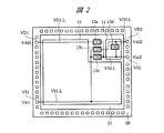
前記半導体装置の外周に、前記第1、第2、第3、第4の電源端子および複数の入出力バッファを含むI/O領域が配置され、
前記I/O領域の内側の領域に、前記第1の回路ブロックと前記第2の回路ブロックとを含むコア領域が配置され、
前記コア領域内に、
前記第1の電源ラインと前記第4の電源ラインとの間に接続された第1のクランプ回路と、
前記第2の電源ラインと前記第3の電源ラインとの間に接続された第2のクランプ回路と、
前記第2の電源ラインと前記第4の電源ラインとの間に接続された第3のクランプ回路とを有し、
前記第2の回路ブロックは、前記第1の回路ブロックよりも回路面積が小さく、
前記第2の回路ブロック内に、さらに、前記第3の電源ラインと前記第4の電源ラインとの間に接続された第4のクランプ回路を有することを特徴とする半導体装置。
Priority Applications (2)
| Application Number | Priority Date | Filing Date | Title |
|---|---|---|---|
| JP2004285593A JP4698996B2 (ja) | 2004-09-30 | 2004-09-30 | 半導体装置 |
| US11/222,780 US20060077601A1 (en) | 2004-09-30 | 2005-09-12 | Semiconductor device |
Applications Claiming Priority (1)
| Application Number | Priority Date | Filing Date | Title |
|---|---|---|---|
| JP2004285593A JP4698996B2 (ja) | 2004-09-30 | 2004-09-30 | 半導体装置 |
Related Child Applications (1)
| Application Number | Title | Priority Date | Filing Date |
|---|---|---|---|
| JP2011002092A Division JP5337173B2 (ja) | 2011-01-07 | 2011-01-07 | 半導体装置 |
Publications (2)
| Publication Number | Publication Date |
|---|---|
| JP2006100606A JP2006100606A (ja) | 2006-04-13 |
| JP4698996B2 true JP4698996B2 (ja) | 2011-06-08 |
Family
ID=36144989
Family Applications (1)
| Application Number | Title | Priority Date | Filing Date |
|---|---|---|---|
| JP2004285593A Expired - Fee Related JP4698996B2 (ja) | 2004-09-30 | 2004-09-30 | 半導体装置 |
Country Status (2)
| Country | Link |
|---|---|
| US (1) | US20060077601A1 (ja) |
| JP (1) | JP4698996B2 (ja) |
Families Citing this family (18)
| Publication number | Priority date | Publication date | Assignee | Title |
|---|---|---|---|---|
| US7401315B2 (en) * | 2005-11-14 | 2008-07-15 | Avago Technologies General Ip Pte Ltd | System and method for implementing package level IP preverification for system on chip devices |
| US7518844B1 (en) * | 2006-02-10 | 2009-04-14 | Integrated Device Technology, Inc. | Over-voltage tolerant ESD protection circuit |
| WO2008021981A2 (en) * | 2006-08-09 | 2008-02-21 | Nexgenix Pharmaceuticals, Llc. | Local treatment of epidermal and dermal hyperproliferative lesions |
| US7511550B2 (en) * | 2006-09-26 | 2009-03-31 | Agere Systems Inc. | Method and apparatus for improving reliability of an integrated circuit having multiple power domains |
| JP4337904B2 (ja) | 2007-04-12 | 2009-09-30 | セイコーエプソン株式会社 | 集積回路装置および電子機器 |
| JP4699417B2 (ja) * | 2007-04-16 | 2011-06-08 | 株式会社リコー | アナログ処理回路およびアナログ集積回路装置および画像読取装置および画像形成装置 |
| JP2009016736A (ja) * | 2007-07-09 | 2009-01-22 | Canon Inc | 半導体集積回路 |
| JP5310100B2 (ja) * | 2009-03-03 | 2013-10-09 | 富士通セミコンダクター株式会社 | 静電気保護回路および半導体装置 |
| JP2011096879A (ja) * | 2009-10-30 | 2011-05-12 | Panasonic Corp | 半導体集積回路 |
| JP5719126B2 (ja) * | 2010-06-16 | 2015-05-13 | ルネサスエレクトロニクス株式会社 | 内部回路と静電保護回路を具備する半導体集積回路 |
| KR20120083610A (ko) * | 2011-01-18 | 2012-07-26 | 삼성전자주식회사 | 반도체 모듈 및 이를 포함하는 시스템 |
| US8531806B2 (en) * | 2011-03-01 | 2013-09-10 | Qualcomm Incorporated | Distributed building blocks of R-C clamping circuitry in semiconductor die core area |
| JP2014207412A (ja) * | 2013-04-16 | 2014-10-30 | 株式会社東芝 | Esd保護回路 |
| WO2014188514A1 (ja) * | 2013-05-21 | 2014-11-27 | ルネサスエレクトロニクス株式会社 | 半導体集積回路装置 |
| JP6503915B2 (ja) | 2015-06-19 | 2019-04-24 | 株式会社ソシオネクスト | 半導体装置 |
| JP6521792B2 (ja) * | 2015-08-10 | 2019-05-29 | ルネサスエレクトロニクス株式会社 | 半導体装置 |
| US20180083441A1 (en) * | 2016-09-20 | 2018-03-22 | Globalfoundries Inc. | Method, apparatus, and system for a semiconductor device having novel electrostatic discharge (esd) protection scheme and circuit |
| JP2018067654A (ja) * | 2016-10-20 | 2018-04-26 | ルネサスエレクトロニクス株式会社 | 半導体集積回路及びそれを備えた半導体装置 |
Family Cites Families (7)
| Publication number | Priority date | Publication date | Assignee | Title |
|---|---|---|---|---|
| JPH04111350A (ja) * | 1990-08-31 | 1992-04-13 | Toshiba Corp | 半導体装置 |
| JPH09321225A (ja) * | 1996-05-30 | 1997-12-12 | Nec Corp | 半導体集積回路装置 |
| US5991135A (en) * | 1998-05-11 | 1999-11-23 | Vlsi Technology, Inc. | System including ESD protection |
| JP2000208718A (ja) * | 1999-01-19 | 2000-07-28 | Matsushita Electric Ind Co Ltd | 半導体装置 |
| US6979908B1 (en) * | 2000-01-11 | 2005-12-27 | Texas Instruments Incorporated | Input/output architecture for integrated circuits with efficient positioning of integrated circuit elements |
| JP2001298157A (ja) * | 2000-04-14 | 2001-10-26 | Nec Corp | 保護回路及びこれを搭載した半導体集積回路 |
| TW502428B (en) * | 2001-09-03 | 2002-09-11 | Faraday Tech Corp | Electrostatic discharge protection circuit for power source terminal with dual trigger voltages |
-
2004
- 2004-09-30 JP JP2004285593A patent/JP4698996B2/ja not_active Expired - Fee Related
-
2005
- 2005-09-12 US US11/222,780 patent/US20060077601A1/en not_active Abandoned
Also Published As
| Publication number | Publication date |
|---|---|
| JP2006100606A (ja) | 2006-04-13 |
| US20060077601A1 (en) | 2006-04-13 |
Similar Documents
| Publication | Publication Date | Title |
|---|---|---|
| JP4698996B2 (ja) | 半導体装置 | |
| US7002379B2 (en) | I/O circuit using low voltage transistors which can tolerate high voltages even when power supplies are powered off | |
| US6504418B1 (en) | Using thick-oxide CMOS devices to interface high voltage integrated circuits | |
| TWI415243B (zh) | 用以減少在積體電路內的靜電放電保護之佔用面積的方法和裝置 | |
| CN101882616B (zh) | 集成电路 | |
| US6300800B1 (en) | Integrated circuit I/O buffer with series P-channel and floating well | |
| JPH11274911A (ja) | 耐電圧性出力バッファ | |
| KR101039856B1 (ko) | 정전기 방전 회로 | |
| KR940001383A (ko) | 출력 버퍼의 정전 방전 보호회로를 구비한 집적회로 | |
| JP2017037949A (ja) | 半導体装置 | |
| US6212050B1 (en) | Circuit and method for protecting input/output stage of a low voltage integrated circuit device from a failure of the internal power supply or in the power-up sequencing of power supplies | |
| US5705941A (en) | Output driver for use in semiconductor integrated circuit | |
| US8830639B2 (en) | ESD protection against charge coupling | |
| JP4114751B2 (ja) | 半導体装置 | |
| JP5337173B2 (ja) | 半導体装置 | |
| US20070091523A1 (en) | ESD protection system for multi-power domain circuitry | |
| US7002372B2 (en) | Moderate current 5V tolerant buffer using a 2.5 volt power supply | |
| US6977524B2 (en) | High current 5V tolerant buffer using a 2.5 volt power supply | |
| US20050237682A1 (en) | Novel ESD protection scheme for core devices | |
| US7256975B2 (en) | ESD protection circuit and method | |
| JPS60224259A (ja) | 半導体集積回路装置 | |
| JP2002270766A (ja) | Esd保護回路 | |
| JP3440972B2 (ja) | サージ保護回路 | |
| JP3800501B2 (ja) | 半導体装置 | |
| KR100225850B1 (ko) | Esd cdm를 방지할 수 있는 반도체 메모리 장치의 pad i/o 회로 |
Legal Events
| Date | Code | Title | Description |
|---|---|---|---|
| A621 | Written request for application examination |
Free format text: JAPANESE INTERMEDIATE CODE: A621 Effective date: 20070921 |
|
| A711 | Notification of change in applicant |
Free format text: JAPANESE INTERMEDIATE CODE: A712 Effective date: 20100528 |
|
| A977 | Report on retrieval |
Free format text: JAPANESE INTERMEDIATE CODE: A971007 Effective date: 20101101 |
|
| A131 | Notification of reasons for refusal |
Free format text: JAPANESE INTERMEDIATE CODE: A131 Effective date: 20101109 |
|
| A521 | Request for written amendment filed |
Free format text: JAPANESE INTERMEDIATE CODE: A523 Effective date: 20110107 |
|
| A01 | Written decision to grant a patent or to grant a registration (utility model) |
Free format text: JAPANESE INTERMEDIATE CODE: A01 Effective date: 20110208 |
|
| A61 | First payment of annual fees (during grant procedure) |
Free format text: JAPANESE INTERMEDIATE CODE: A61 Effective date: 20110302 |
|
| S531 | Written request for registration of change of domicile |
Free format text: JAPANESE INTERMEDIATE CODE: R313531 |
|
| R350 | Written notification of registration of transfer |
Free format text: JAPANESE INTERMEDIATE CODE: R350 |
|
| LAPS | Cancellation because of no payment of annual fees |