JP4686300B2 - デバイス支持構造体及びこれの製造方法 - Google Patents
デバイス支持構造体及びこれの製造方法 Download PDFInfo
- Publication number
- JP4686300B2 JP4686300B2 JP2005238111A JP2005238111A JP4686300B2 JP 4686300 B2 JP4686300 B2 JP 4686300B2 JP 2005238111 A JP2005238111 A JP 2005238111A JP 2005238111 A JP2005238111 A JP 2005238111A JP 4686300 B2 JP4686300 B2 JP 4686300B2
- Authority
- JP
- Japan
- Prior art keywords
- lead
- free solder
- support
- connector
- compressible film
- Prior art date
- Legal status (The legal status is an assumption and is not a legal conclusion. Google has not performed a legal analysis and makes no representation as to the accuracy of the status listed.)
- Expired - Fee Related
Links
Images


Classifications
-
- H—ELECTRICITY
- H01—ELECTRIC ELEMENTS
- H01L—SEMICONDUCTOR DEVICES NOT COVERED BY CLASS H10
- H01L21/00—Processes or apparatus adapted for the manufacture or treatment of semiconductor or solid state devices or of parts thereof
- H01L21/02—Manufacture or treatment of semiconductor devices or of parts thereof
- H01L21/04—Manufacture or treatment of semiconductor devices or of parts thereof the devices having at least one potential-jump barrier or surface barrier, e.g. PN junction, depletion layer or carrier concentration layer
- H01L21/50—Assembly of semiconductor devices using processes or apparatus not provided for in a single one of the subgroups H01L21/06 - H01L21/326, e.g. sealing of a cap to a base of a container
- H01L21/56—Encapsulations, e.g. encapsulation layers, coatings
- H01L21/563—Encapsulation of active face of flip-chip device, e.g. underfilling or underencapsulation of flip-chip, encapsulation preform on chip or mounting substrate
-
- H—ELECTRICITY
- H01—ELECTRIC ELEMENTS
- H01L—SEMICONDUCTOR DEVICES NOT COVERED BY CLASS H10
- H01L24/00—Arrangements for connecting or disconnecting semiconductor or solid-state bodies; Methods or apparatus related thereto
- H01L24/01—Means for bonding being attached to, or being formed on, the surface to be connected, e.g. chip-to-package, die-attach, "first-level" interconnects; Manufacturing methods related thereto
- H01L24/10—Bump connectors ; Manufacturing methods related thereto
- H01L24/12—Structure, shape, material or disposition of the bump connectors prior to the connecting process
-
- H—ELECTRICITY
- H01—ELECTRIC ELEMENTS
- H01L—SEMICONDUCTOR DEVICES NOT COVERED BY CLASS H10
- H01L24/00—Arrangements for connecting or disconnecting semiconductor or solid-state bodies; Methods or apparatus related thereto
- H01L24/80—Methods for connecting semiconductor or other solid state bodies using means for bonding being attached to, or being formed on, the surface to be connected
- H01L24/81—Methods for connecting semiconductor or other solid state bodies using means for bonding being attached to, or being formed on, the surface to be connected using a bump connector
-
- H—ELECTRICITY
- H05—ELECTRIC TECHNIQUES NOT OTHERWISE PROVIDED FOR
- H05K—PRINTED CIRCUITS; CASINGS OR CONSTRUCTIONAL DETAILS OF ELECTRIC APPARATUS; MANUFACTURE OF ASSEMBLAGES OF ELECTRICAL COMPONENTS
- H05K3/00—Apparatus or processes for manufacturing printed circuits
- H05K3/30—Assembling printed circuits with electric components, e.g. with resistor
- H05K3/32—Assembling printed circuits with electric components, e.g. with resistor electrically connecting electric components or wires to printed circuits
- H05K3/34—Assembling printed circuits with electric components, e.g. with resistor electrically connecting electric components or wires to printed circuits by soldering
- H05K3/341—Surface mounted components
- H05K3/3431—Leadless components
- H05K3/3436—Leadless components having an array of bottom contacts, e.g. pad grid array or ball grid array components
-
- H—ELECTRICITY
- H01—ELECTRIC ELEMENTS
- H01L—SEMICONDUCTOR DEVICES NOT COVERED BY CLASS H10
- H01L2224/00—Indexing scheme for arrangements for connecting or disconnecting semiconductor or solid-state bodies and methods related thereto as covered by H01L24/00
- H01L2224/01—Means for bonding being attached to, or being formed on, the surface to be connected, e.g. chip-to-package, die-attach, "first-level" interconnects; Manufacturing methods related thereto
- H01L2224/10—Bump connectors; Manufacturing methods related thereto
- H01L2224/1012—Auxiliary members for bump connectors, e.g. spacers
- H01L2224/10122—Auxiliary members for bump connectors, e.g. spacers being formed on the semiconductor or solid-state body to be connected
- H01L2224/10125—Reinforcing structures
- H01L2224/10126—Bump collar
-
- H—ELECTRICITY
- H01—ELECTRIC ELEMENTS
- H01L—SEMICONDUCTOR DEVICES NOT COVERED BY CLASS H10
- H01L2224/00—Indexing scheme for arrangements for connecting or disconnecting semiconductor or solid-state bodies and methods related thereto as covered by H01L24/00
- H01L2224/01—Means for bonding being attached to, or being formed on, the surface to be connected, e.g. chip-to-package, die-attach, "first-level" interconnects; Manufacturing methods related thereto
- H01L2224/10—Bump connectors; Manufacturing methods related thereto
- H01L2224/12—Structure, shape, material or disposition of the bump connectors prior to the connecting process
- H01L2224/13—Structure, shape, material or disposition of the bump connectors prior to the connecting process of an individual bump connector
- H01L2224/13001—Core members of the bump connector
- H01L2224/13099—Material
- H01L2224/131—Material with a principal constituent of the material being a metal or a metalloid, e.g. boron [B], silicon [Si], germanium [Ge], arsenic [As], antimony [Sb], tellurium [Te] and polonium [Po], and alloys thereof
-
- H—ELECTRICITY
- H01—ELECTRIC ELEMENTS
- H01L—SEMICONDUCTOR DEVICES NOT COVERED BY CLASS H10
- H01L2224/00—Indexing scheme for arrangements for connecting or disconnecting semiconductor or solid-state bodies and methods related thereto as covered by H01L24/00
- H01L2224/01—Means for bonding being attached to, or being formed on, the surface to be connected, e.g. chip-to-package, die-attach, "first-level" interconnects; Manufacturing methods related thereto
- H01L2224/10—Bump connectors; Manufacturing methods related thereto
- H01L2224/12—Structure, shape, material or disposition of the bump connectors prior to the connecting process
- H01L2224/13—Structure, shape, material or disposition of the bump connectors prior to the connecting process of an individual bump connector
- H01L2224/1354—Coating
- H01L2224/1356—Disposition
- H01L2224/13563—Only on parts of the surface of the core, i.e. partial coating
- H01L2224/13566—Both on and outside the bonding interface of the bump connector
-
- H—ELECTRICITY
- H01—ELECTRIC ELEMENTS
- H01L—SEMICONDUCTOR DEVICES NOT COVERED BY CLASS H10
- H01L2224/00—Indexing scheme for arrangements for connecting or disconnecting semiconductor or solid-state bodies and methods related thereto as covered by H01L24/00
- H01L2224/01—Means for bonding being attached to, or being formed on, the surface to be connected, e.g. chip-to-package, die-attach, "first-level" interconnects; Manufacturing methods related thereto
- H01L2224/10—Bump connectors; Manufacturing methods related thereto
- H01L2224/15—Structure, shape, material or disposition of the bump connectors after the connecting process
- H01L2224/16—Structure, shape, material or disposition of the bump connectors after the connecting process of an individual bump connector
-
- H—ELECTRICITY
- H01—ELECTRIC ELEMENTS
- H01L—SEMICONDUCTOR DEVICES NOT COVERED BY CLASS H10
- H01L2224/00—Indexing scheme for arrangements for connecting or disconnecting semiconductor or solid-state bodies and methods related thereto as covered by H01L24/00
- H01L2224/73—Means for bonding being of different types provided for in two or more of groups H01L2224/10, H01L2224/18, H01L2224/26, H01L2224/34, H01L2224/42, H01L2224/50, H01L2224/63, H01L2224/71
- H01L2224/732—Location after the connecting process
- H01L2224/73201—Location after the connecting process on the same surface
- H01L2224/73203—Bump and layer connectors
-
- H—ELECTRICITY
- H01—ELECTRIC ELEMENTS
- H01L—SEMICONDUCTOR DEVICES NOT COVERED BY CLASS H10
- H01L2224/00—Indexing scheme for arrangements for connecting or disconnecting semiconductor or solid-state bodies and methods related thereto as covered by H01L24/00
- H01L2224/80—Methods for connecting semiconductor or other solid state bodies using means for bonding being attached to, or being formed on, the surface to be connected
- H01L2224/81—Methods for connecting semiconductor or other solid state bodies using means for bonding being attached to, or being formed on, the surface to be connected using a bump connector
- H01L2224/812—Applying energy for connecting
- H01L2224/8121—Applying energy for connecting using a reflow oven
-
- H—ELECTRICITY
- H01—ELECTRIC ELEMENTS
- H01L—SEMICONDUCTOR DEVICES NOT COVERED BY CLASS H10
- H01L2224/00—Indexing scheme for arrangements for connecting or disconnecting semiconductor or solid-state bodies and methods related thereto as covered by H01L24/00
- H01L2224/80—Methods for connecting semiconductor or other solid state bodies using means for bonding being attached to, or being formed on, the surface to be connected
- H01L2224/81—Methods for connecting semiconductor or other solid state bodies using means for bonding being attached to, or being formed on, the surface to be connected using a bump connector
- H01L2224/818—Bonding techniques
- H01L2224/81801—Soldering or alloying
- H01L2224/81815—Reflow soldering
-
- H—ELECTRICITY
- H01—ELECTRIC ELEMENTS
- H01L—SEMICONDUCTOR DEVICES NOT COVERED BY CLASS H10
- H01L23/00—Details of semiconductor or other solid state devices
- H01L23/28—Encapsulations, e.g. encapsulating layers, coatings, e.g. for protection
- H01L23/31—Encapsulations, e.g. encapsulating layers, coatings, e.g. for protection characterised by the arrangement or shape
- H01L23/3157—Partial encapsulation or coating
- H01L23/3171—Partial encapsulation or coating the coating being directly applied to the semiconductor body, e.g. passivation layer
-
- H—ELECTRICITY
- H01—ELECTRIC ELEMENTS
- H01L—SEMICONDUCTOR DEVICES NOT COVERED BY CLASS H10
- H01L24/00—Arrangements for connecting or disconnecting semiconductor or solid-state bodies; Methods or apparatus related thereto
- H01L24/01—Means for bonding being attached to, or being formed on, the surface to be connected, e.g. chip-to-package, die-attach, "first-level" interconnects; Manufacturing methods related thereto
- H01L24/10—Bump connectors ; Manufacturing methods related thereto
- H01L24/15—Structure, shape, material or disposition of the bump connectors after the connecting process
- H01L24/16—Structure, shape, material or disposition of the bump connectors after the connecting process of an individual bump connector
-
- H—ELECTRICITY
- H01—ELECTRIC ELEMENTS
- H01L—SEMICONDUCTOR DEVICES NOT COVERED BY CLASS H10
- H01L2924/00—Indexing scheme for arrangements or methods for connecting or disconnecting semiconductor or solid-state bodies as covered by H01L24/00
- H01L2924/0001—Technical content checked by a classifier
- H01L2924/00011—Not relevant to the scope of the group, the symbol of which is combined with the symbol of this group
-
- H—ELECTRICITY
- H01—ELECTRIC ELEMENTS
- H01L—SEMICONDUCTOR DEVICES NOT COVERED BY CLASS H10
- H01L2924/00—Indexing scheme for arrangements or methods for connecting or disconnecting semiconductor or solid-state bodies as covered by H01L24/00
- H01L2924/0001—Technical content checked by a classifier
- H01L2924/00013—Fully indexed content
-
- H—ELECTRICITY
- H01—ELECTRIC ELEMENTS
- H01L—SEMICONDUCTOR DEVICES NOT COVERED BY CLASS H10
- H01L2924/00—Indexing scheme for arrangements or methods for connecting or disconnecting semiconductor or solid-state bodies as covered by H01L24/00
- H01L2924/0001—Technical content checked by a classifier
- H01L2924/00014—Technical content checked by a classifier the subject-matter covered by the group, the symbol of which is combined with the symbol of this group, being disclosed without further technical details
-
- H—ELECTRICITY
- H01—ELECTRIC ELEMENTS
- H01L—SEMICONDUCTOR DEVICES NOT COVERED BY CLASS H10
- H01L2924/00—Indexing scheme for arrangements or methods for connecting or disconnecting semiconductor or solid-state bodies as covered by H01L24/00
- H01L2924/01—Chemical elements
- H01L2924/01004—Beryllium [Be]
-
- H—ELECTRICITY
- H01—ELECTRIC ELEMENTS
- H01L—SEMICONDUCTOR DEVICES NOT COVERED BY CLASS H10
- H01L2924/00—Indexing scheme for arrangements or methods for connecting or disconnecting semiconductor or solid-state bodies as covered by H01L24/00
- H01L2924/01—Chemical elements
- H01L2924/01006—Carbon [C]
-
- H—ELECTRICITY
- H01—ELECTRIC ELEMENTS
- H01L—SEMICONDUCTOR DEVICES NOT COVERED BY CLASS H10
- H01L2924/00—Indexing scheme for arrangements or methods for connecting or disconnecting semiconductor or solid-state bodies as covered by H01L24/00
- H01L2924/01—Chemical elements
- H01L2924/01029—Copper [Cu]
-
- H—ELECTRICITY
- H01—ELECTRIC ELEMENTS
- H01L—SEMICONDUCTOR DEVICES NOT COVERED BY CLASS H10
- H01L2924/00—Indexing scheme for arrangements or methods for connecting or disconnecting semiconductor or solid-state bodies as covered by H01L24/00
- H01L2924/01—Chemical elements
- H01L2924/01033—Arsenic [As]
-
- H—ELECTRICITY
- H01—ELECTRIC ELEMENTS
- H01L—SEMICONDUCTOR DEVICES NOT COVERED BY CLASS H10
- H01L2924/00—Indexing scheme for arrangements or methods for connecting or disconnecting semiconductor or solid-state bodies as covered by H01L24/00
- H01L2924/01—Chemical elements
- H01L2924/01047—Silver [Ag]
-
- H—ELECTRICITY
- H01—ELECTRIC ELEMENTS
- H01L—SEMICONDUCTOR DEVICES NOT COVERED BY CLASS H10
- H01L2924/00—Indexing scheme for arrangements or methods for connecting or disconnecting semiconductor or solid-state bodies as covered by H01L24/00
- H01L2924/01—Chemical elements
- H01L2924/01075—Rhenium [Re]
-
- H—ELECTRICITY
- H01—ELECTRIC ELEMENTS
- H01L—SEMICONDUCTOR DEVICES NOT COVERED BY CLASS H10
- H01L2924/00—Indexing scheme for arrangements or methods for connecting or disconnecting semiconductor or solid-state bodies as covered by H01L24/00
- H01L2924/01—Chemical elements
- H01L2924/01082—Lead [Pb]
-
- H—ELECTRICITY
- H01—ELECTRIC ELEMENTS
- H01L—SEMICONDUCTOR DEVICES NOT COVERED BY CLASS H10
- H01L2924/00—Indexing scheme for arrangements or methods for connecting or disconnecting semiconductor or solid-state bodies as covered by H01L24/00
- H01L2924/013—Alloys
- H01L2924/014—Solder alloys
-
- H—ELECTRICITY
- H01—ELECTRIC ELEMENTS
- H01L—SEMICONDUCTOR DEVICES NOT COVERED BY CLASS H10
- H01L2924/00—Indexing scheme for arrangements or methods for connecting or disconnecting semiconductor or solid-state bodies as covered by H01L24/00
- H01L2924/10—Details of semiconductor or other solid state devices to be connected
- H01L2924/11—Device type
- H01L2924/14—Integrated circuits
-
- H—ELECTRICITY
- H01—ELECTRIC ELEMENTS
- H01R—ELECTRICALLY-CONDUCTIVE CONNECTIONS; STRUCTURAL ASSOCIATIONS OF A PLURALITY OF MUTUALLY-INSULATED ELECTRICAL CONNECTING ELEMENTS; COUPLING DEVICES; CURRENT COLLECTORS
- H01R43/00—Apparatus or processes specially adapted for manufacturing, assembling, maintaining, or repairing of line connectors or current collectors or for joining electric conductors
- H01R43/02—Apparatus or processes specially adapted for manufacturing, assembling, maintaining, or repairing of line connectors or current collectors or for joining electric conductors for soldered or welded connections
- H01R43/0256—Apparatus or processes specially adapted for manufacturing, assembling, maintaining, or repairing of line connectors or current collectors or for joining electric conductors for soldered or welded connections for soldering or welding connectors to a printed circuit board
-
- H—ELECTRICITY
- H05—ELECTRIC TECHNIQUES NOT OTHERWISE PROVIDED FOR
- H05K—PRINTED CIRCUITS; CASINGS OR CONSTRUCTIONAL DETAILS OF ELECTRIC APPARATUS; MANUFACTURE OF ASSEMBLAGES OF ELECTRICAL COMPONENTS
- H05K2201/00—Indexing scheme relating to printed circuits covered by H05K1/00
- H05K2201/01—Dielectrics
- H05K2201/0104—Properties and characteristics in general
- H05K2201/0133—Elastomeric or compliant polymer
-
- H—ELECTRICITY
- H05—ELECTRIC TECHNIQUES NOT OTHERWISE PROVIDED FOR
- H05K—PRINTED CIRCUITS; CASINGS OR CONSTRUCTIONAL DETAILS OF ELECTRIC APPARATUS; MANUFACTURE OF ASSEMBLAGES OF ELECTRICAL COMPONENTS
- H05K2201/00—Indexing scheme relating to printed circuits covered by H05K1/00
- H05K2201/10—Details of components or other objects attached to or integrated in a printed circuit board
- H05K2201/10613—Details of electrical connections of non-printed components, e.g. special leads
- H05K2201/10954—Other details of electrical connections
- H05K2201/10977—Encapsulated connections
-
- H—ELECTRICITY
- H05—ELECTRIC TECHNIQUES NOT OTHERWISE PROVIDED FOR
- H05K—PRINTED CIRCUITS; CASINGS OR CONSTRUCTIONAL DETAILS OF ELECTRIC APPARATUS; MANUFACTURE OF ASSEMBLAGES OF ELECTRICAL COMPONENTS
- H05K3/00—Apparatus or processes for manufacturing printed circuits
- H05K3/22—Secondary treatment of printed circuits
- H05K3/28—Applying non-metallic protective coatings
- H05K3/284—Applying non-metallic protective coatings for encapsulating mounted components
-
- Y—GENERAL TAGGING OF NEW TECHNOLOGICAL DEVELOPMENTS; GENERAL TAGGING OF CROSS-SECTIONAL TECHNOLOGIES SPANNING OVER SEVERAL SECTIONS OF THE IPC; TECHNICAL SUBJECTS COVERED BY FORMER USPC CROSS-REFERENCE ART COLLECTIONS [XRACs] AND DIGESTS
- Y02—TECHNOLOGIES OR APPLICATIONS FOR MITIGATION OR ADAPTATION AGAINST CLIMATE CHANGE
- Y02P—CLIMATE CHANGE MITIGATION TECHNOLOGIES IN THE PRODUCTION OR PROCESSING OF GOODS
- Y02P70/00—Climate change mitigation technologies in the production process for final industrial or consumer products
- Y02P70/50—Manufacturing or production processes characterised by the final manufactured product
Description
本発明は図面を参照しながら以下の詳細な説明からより一層理解されるであろう。
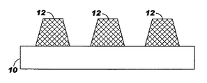
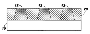
12:コネクタ
20:圧縮性材料
30:マスク
60:支持体
62:アンダーフィル
90:チャネル
Claims (15)
- 支持体と、
前記支持体に結合されるデバイスと、
前記デバイスの表面から突出し該デバイスを前記支持体に電気接続する複数個の無鉛ハンダコネクタと、
隣接する無鉛ハンダコネクタ相互間に隙間を形成するように前記複数個の無鉛ハンダコネクタのそれぞれの側面を囲む圧縮性フィルムであって、前記圧縮性フィルムは前記無鉛ハンダコネクタの融点以上で熱的に安定であり、前記無鉛ハンダコネクタのリフロー時の体積膨張を吸収する、前記圧縮性フィルムと、
前記圧縮性フィルムに接し、前記支持体と前記デバイスの前記表面との間の前記隙間を埋める絶縁性のアンダーフィルと、
を含むデバイス支持構造体。 - 前記圧縮性フィルムは、複数個の前記無鉛ハンダコネクタを囲む正方形または矩形のパターンにパターン化されている、請求項1に記載の構造体。
- 前記パターンは、該パターン相互間に前記隙間に対応するチャネルを形成するように配置されている、請求項2に記載の構造体。
- 前記無鉛ハンダコネクタは、SnAgCuハンダである、請求項1に記載の構造体。
- 前記圧縮性フィルムの材料は、シリコンゴム又はポリイミド発泡体である、請求項1に記載の構造体。
- デバイスの表面上に該表面から突出する複数個の無鉛ハンダコネクタを形成するステップと、
隣接する無鉛ハンダコネクタ相互間に隙間を形成するように前記複数個の無鉛ハンダコネクタのそれぞれの側面を圧縮性フィルムで囲むステップであって、前記圧縮性フィルムは前記無鉛ハンダコネクタの融点以上で熱的に安定であり、前記無鉛ハンダコネクタのリフロー時の体積膨張を吸収する、前記ステップと、
前記デバイスの前記複数個の無鉛ハンダコネクタを支持体に位置決めして前記無鉛ハンダコネクタをリフローすることにより前記デバイスを前記支持体に電気的に接続するステップと、
前記支持体と前記デバイスの前記表面との間の前記隙間を絶縁性のアンダーフィルで埋めるステップとを含むデバイス支持構造体を製造する方法。 - 前記圧縮性フィルムは、複数個の前記無鉛ハンダコネクタを囲む正方形または矩形のパターンにパターン化されている、請求項6に記載の方法。
- 前記パターンは、該パターン相互間に前記隙間に対応するチャネルを形成するように配置されている、請求項7に記載の方法。
- 前記無鉛ハンダコネクタは、SnAgCuハンダである、請求項6に記載の方法。
- 前記圧縮性フィルムの材料は、シリコンゴム又はポリイミド発泡体である、請求項6に記載の方法。
- デバイスの表面上に該表面から突出する複数個の無鉛ハンダコネクタを形成ステップと、
前記複数個の無鉛ハンダコネクタ相互間を埋めるように前記デバイスの表面に圧縮性フィルムを付着するステップであって、前記圧縮性フィルムは前記無鉛ハンダコネクタの融点以上で熱的に安定であり、前記無鉛ハンダコネクタのリフロー時の体積膨張を吸収する、前記ステップと、
前記無鉛ハンダコネクタの上面と、前記圧縮性フィルムの上面のうち前記無鉛ハンダコネクタの上面に隣接する一部分とを覆うマスクを形成するステップと、
前記マスクを介して前記圧縮性フィルムをパターン化することにより、隣接する無鉛ハンダコネクタ相互間に隙間を形成するように前記複数個の無鉛ハンダコネクタのそれぞれの側面に圧縮性フィルムを残すステップと、
前記マスクを除去し、前記デバイスの前記複数個の無鉛ハンダコネクタを支持体に位置決めして前記無鉛ハンダコネクタをリフローすることにより前記デバイスを前記支持体に電気的に接続するステップと、
前記支持体と前記デバイスの前記表面との間の前記隙間を絶縁性のアンダーフィルで埋めるステップとを含むデバイス支持構造体を製造する方法。 - 前記圧縮性フィルムは、複数個の前記無鉛ハンダコネクタを囲む正方形または矩形のパターンにパターン化されている、請求項11に記載の方法。
- 前記パターンは、該パターン相互間に前記隙間に対応するチャネルを形成するように配置されている、請求項12に記載の方法。
- 前記無鉛ハンダコネクタは、SnAgCuハンダである、請求項11に記載の方法。
- 前記圧縮性フィルムの材料は、シリコンゴム又はポリイミド発泡体である、請求項11に記載の方法
Applications Claiming Priority (2)
| Application Number | Priority Date | Filing Date | Title |
|---|---|---|---|
| US10/711076 | 2004-08-20 | ||
| US10/711,076 US7332821B2 (en) | 2004-08-20 | 2004-08-20 | Compressible films surrounding solder connectors |
Publications (3)
| Publication Number | Publication Date |
|---|---|
| JP2006059814A JP2006059814A (ja) | 2006-03-02 |
| JP2006059814A5 JP2006059814A5 (ja) | 2008-07-10 |
| JP4686300B2 true JP4686300B2 (ja) | 2011-05-25 |
Family
ID=35910206
Family Applications (1)
| Application Number | Title | Priority Date | Filing Date |
|---|---|---|---|
| JP2005238111A Expired - Fee Related JP4686300B2 (ja) | 2004-08-20 | 2005-08-19 | デバイス支持構造体及びこれの製造方法 |
Country Status (4)
| Country | Link |
|---|---|
| US (2) | US7332821B2 (ja) |
| JP (1) | JP4686300B2 (ja) |
| CN (1) | CN100399560C (ja) |
| TW (1) | TWI346518B (ja) |
Families Citing this family (16)
| Publication number | Priority date | Publication date | Assignee | Title |
|---|---|---|---|---|
| WO2006056999A2 (en) * | 2004-11-29 | 2006-06-01 | N-Trig Ltd. | Methods for manufacturing a sensor assembly |
| US20070063344A1 (en) * | 2005-09-22 | 2007-03-22 | Chun-Hung Lin | Chip package structure and bumping process |
| WO2007114111A1 (ja) * | 2006-03-28 | 2007-10-11 | Matsushita Electric Industrial Co., Ltd. | 多層配線基板とその製造方法 |
| US7727805B2 (en) * | 2007-06-11 | 2010-06-01 | Intel Corporation | Reducing stress in a flip chip assembly |
| US20090108442A1 (en) * | 2007-10-25 | 2009-04-30 | International Business Machines Corporation | Self-assembled stress relief interface |
| US8507325B2 (en) | 2010-01-28 | 2013-08-13 | International Business Machines Corporation | Co-axial restraint for connectors within flip-chip packages |
| FR2957748B1 (fr) * | 2010-03-16 | 2012-09-07 | St Microelectronics Grenoble 2 | Composant electronique a montage en surface |
| US9082780B2 (en) * | 2012-03-23 | 2015-07-14 | Stats Chippac, Ltd. | Semiconductor device and method of forming a robust fan-out package including vertical interconnects and mechanical support layer |
| US20140291834A1 (en) * | 2013-03-27 | 2014-10-02 | Micron Technology, Inc. | Semiconductor devices and packages including conductive underfill material and related methods |
| US9711474B2 (en) * | 2014-09-24 | 2017-07-18 | Taiwan Semiconductor Manufacturing Company Ltd. | Semiconductor package structure with polymeric layer and manufacturing method thereof |
| US20170309584A1 (en) * | 2014-10-23 | 2017-10-26 | Agency For Science, Technology And Research | Method of bonding a first substrate and a second substrate |
| KR102458034B1 (ko) | 2015-10-16 | 2022-10-25 | 삼성전자주식회사 | 반도체 패키지, 반도체 패키지의 제조방법, 및 반도체 모듈 |
| US10597486B2 (en) | 2016-11-02 | 2020-03-24 | Seagate Technology Llc | Encapsulant composition for use with electrical components in hard disk drives, and related electrical components and hard disk drives |
| US10163847B2 (en) * | 2017-03-03 | 2018-12-25 | Tdk Corporation | Method for producing semiconductor package |
| CN108538726B (zh) * | 2017-03-03 | 2022-08-26 | Tdk株式会社 | 半导体芯片的制造方法 |
| WO2021222582A1 (en) * | 2020-04-30 | 2021-11-04 | Dujud Llc | Methods and processes for forming electrical circuitries on three-dimensional geometries |
Citations (5)
| Publication number | Priority date | Publication date | Assignee | Title |
|---|---|---|---|---|
| JPH10178121A (ja) * | 1996-12-18 | 1998-06-30 | Toshiba Corp | 半導体パッケージ用金属ボール配設板、半導体装置及びその製造方法 |
| WO1999050906A1 (en) * | 1998-03-27 | 1999-10-07 | Seiko Epson Corporation | Semiconductor device and method for manufacturing the same, circuit substrate, and electronic device |
| JP2001007502A (ja) * | 1999-06-23 | 2001-01-12 | Sony Corp | 電子部品パッケージの接続構造及び接続方法 |
| JP2001313315A (ja) * | 2001-04-25 | 2001-11-09 | Hitachi Ltd | 実装用半導体装置とその実装方法 |
| JP2004103928A (ja) * | 2002-09-11 | 2004-04-02 | Fujitsu Ltd | 基板及びハンダボールの形成方法及びその実装構造 |
Family Cites Families (17)
| Publication number | Priority date | Publication date | Assignee | Title |
|---|---|---|---|---|
| US5274913A (en) * | 1991-10-25 | 1994-01-04 | International Business Machines Corporation | Method of fabricating a reworkable module |
| US5956605A (en) * | 1996-09-20 | 1999-09-21 | Micron Technology, Inc. | Use of nitrides for flip-chip encapsulation |
| DE1025587T1 (de) * | 1997-07-21 | 2001-02-08 | Aguila Technologies Inc | Halbleiter-flipchippackung und herstellungsverfahren dafür |
| US6100114A (en) * | 1998-08-10 | 2000-08-08 | International Business Machines Corporation | Encapsulation of solder bumps and solder connections |
| US6281452B1 (en) * | 1998-12-03 | 2001-08-28 | International Business Machines Corporation | Multi-level thin-film electronic packaging structure and related method |
| US6225206B1 (en) * | 1999-05-10 | 2001-05-01 | International Business Machines Corporation | Flip chip C4 extension structure and process |
| JP2001127108A (ja) | 1999-10-25 | 2001-05-11 | Hitachi Ltd | 半導体装置 |
| US6700209B1 (en) * | 1999-12-29 | 2004-03-02 | Intel Corporation | Partial underfill for flip-chip electronic packages |
| JP2001339012A (ja) * | 2000-05-30 | 2001-12-07 | Nec Kyushu Ltd | 半導体装置およびその製造方法 |
| US6680436B2 (en) * | 2000-07-12 | 2004-01-20 | Seagate Technology Llc | Reflow encapsulant |
| US6573122B2 (en) * | 2001-03-28 | 2003-06-03 | International Rectifier Corporation | Wafer level insulation underfill for die attach |
| US20020180029A1 (en) * | 2001-04-25 | 2002-12-05 | Hideki Higashitani | Semiconductor device with intermediate connector |
| TW544826B (en) * | 2001-05-18 | 2003-08-01 | Nec Electronics Corp | Flip-chip-type semiconductor device and manufacturing method thereof |
| JP3708478B2 (ja) * | 2001-11-20 | 2005-10-19 | 松下電器産業株式会社 | 電子部品の実装方法 |
| JP2003234362A (ja) * | 2002-02-12 | 2003-08-22 | Yokogawa Electric Corp | 半導体装置 |
| TW540123B (en) * | 2002-06-14 | 2003-07-01 | Siliconware Precision Industries Co Ltd | Flip-chip semiconductor package with lead frame as chip carrier |
| US6921860B2 (en) * | 2003-03-18 | 2005-07-26 | Micron Technology, Inc. | Microelectronic component assemblies having exposed contacts |
-
2004
- 2004-08-20 US US10/711,076 patent/US7332821B2/en not_active Expired - Fee Related
-
2005
- 2005-04-29 CN CNB2005100684327A patent/CN100399560C/zh not_active Expired - Fee Related
- 2005-08-02 TW TW094126235A patent/TWI346518B/zh not_active IP Right Cessation
- 2005-08-19 JP JP2005238111A patent/JP4686300B2/ja not_active Expired - Fee Related
-
2007
- 2007-09-20 US US11/858,147 patent/US7566649B2/en not_active Expired - Fee Related
Patent Citations (5)
| Publication number | Priority date | Publication date | Assignee | Title |
|---|---|---|---|---|
| JPH10178121A (ja) * | 1996-12-18 | 1998-06-30 | Toshiba Corp | 半導体パッケージ用金属ボール配設板、半導体装置及びその製造方法 |
| WO1999050906A1 (en) * | 1998-03-27 | 1999-10-07 | Seiko Epson Corporation | Semiconductor device and method for manufacturing the same, circuit substrate, and electronic device |
| JP2001007502A (ja) * | 1999-06-23 | 2001-01-12 | Sony Corp | 電子部品パッケージの接続構造及び接続方法 |
| JP2001313315A (ja) * | 2001-04-25 | 2001-11-09 | Hitachi Ltd | 実装用半導体装置とその実装方法 |
| JP2004103928A (ja) * | 2002-09-11 | 2004-04-02 | Fujitsu Ltd | 基板及びハンダボールの形成方法及びその実装構造 |
Also Published As
| Publication number | Publication date |
|---|---|
| JP2006059814A (ja) | 2006-03-02 |
| TWI346518B (en) | 2011-08-01 |
| US7566649B2 (en) | 2009-07-28 |
| CN1738042A (zh) | 2006-02-22 |
| TW200618685A (en) | 2006-06-01 |
| US20080009101A1 (en) | 2008-01-10 |
| CN100399560C (zh) | 2008-07-02 |
| US20060040567A1 (en) | 2006-02-23 |
| US7332821B2 (en) | 2008-02-19 |
Similar Documents
| Publication | Publication Date | Title |
|---|---|---|
| JP4686300B2 (ja) | デバイス支持構造体及びこれの製造方法 | |
| TWI378516B (en) | Bump-on-lead flip chip interconnection | |
| US6828669B2 (en) | Interconnection substrate having metal columns covered by a resin film, and manufacturing method thereof | |
| KR101328551B1 (ko) | 반도체 장치 | |
| JP5923725B2 (ja) | 電子部品の実装構造体 | |
| CN108695264B (zh) | 半导体器件 | |
| KR100687000B1 (ko) | 반도체 장치의 제조 방법 및 전기적 접속부의 처리 방법 | |
| JP2006128662A (ja) | 半導体装置およびその実装体 | |
| US20180337106A1 (en) | Bump-on-trace packaging structure and method for forming the same | |
| US20060022320A1 (en) | Semiconductor device and manufacturing method thereof | |
| JP6547745B2 (ja) | 半導体装置およびその製造方法 | |
| JP2006202969A (ja) | 半導体装置およびその実装体 | |
| JP4963998B2 (ja) | 回路基板、半導体装置、及び半田バンプの形成方法 | |
| JP2010157693A (ja) | 金属バンプを備えた半導体パッケージ基板 | |
| JP6544354B2 (ja) | 半導体装置の製造方法 | |
| JP4835406B2 (ja) | 実装構造体とその製造方法および半導体装置とその製造方法 | |
| US6956293B2 (en) | Semiconductor device | |
| JP4267549B2 (ja) | 半導体装置およびその製造方法ならびに電子機器 | |
| JP2006108182A (ja) | 半導体装置およびその実装体およびその製造方法 | |
| JP7197967B2 (ja) | リードフレーム構造の製造方法、並びに半導体装置の製造方法及び積層半導体装置の製造方法 | |
| JP2001168224A (ja) | 半導体装置、電子回路装置および製造方法 | |
| JP2006108181A (ja) | 半導体装置およびその製造方法およびその実装体 | |
| JP2004253598A (ja) | 電子部品の実装方法 | |
| JP2006041559A (ja) | 半導体装置及び電子機器 | |
| KR101133126B1 (ko) | 반도체 패키지 및 그 제조 방법 |
Legal Events
| Date | Code | Title | Description |
|---|---|---|---|
| A521 | Request for written amendment filed |
Free format text: JAPANESE INTERMEDIATE CODE: A523 Effective date: 20080528 |
|
| A621 | Written request for application examination |
Free format text: JAPANESE INTERMEDIATE CODE: A621 Effective date: 20080528 |
|
| A521 | Request for written amendment filed |
Free format text: JAPANESE INTERMEDIATE CODE: A523 Effective date: 20090206 |
|
| A977 | Report on retrieval |
Free format text: JAPANESE INTERMEDIATE CODE: A971007 Effective date: 20100818 |
|
| A131 | Notification of reasons for refusal |
Free format text: JAPANESE INTERMEDIATE CODE: A131 Effective date: 20100824 |
|
| A521 | Request for written amendment filed |
Free format text: JAPANESE INTERMEDIATE CODE: A523 Effective date: 20101118 |
|
| TRDD | Decision of grant or rejection written | ||
| A01 | Written decision to grant a patent or to grant a registration (utility model) |
Free format text: JAPANESE INTERMEDIATE CODE: A01 Effective date: 20110201 |
|
| A01 | Written decision to grant a patent or to grant a registration (utility model) |
Free format text: JAPANESE INTERMEDIATE CODE: A01 |
|
| A61 | First payment of annual fees (during grant procedure) |
Free format text: JAPANESE INTERMEDIATE CODE: A61 Effective date: 20110214 |
|
| FPAY | Renewal fee payment (event date is renewal date of database) |
Free format text: PAYMENT UNTIL: 20140218 Year of fee payment: 3 |
|
| R150 | Certificate of patent or registration of utility model |
Free format text: JAPANESE INTERMEDIATE CODE: R150 |
|
| S111 | Request for change of ownership or part of ownership |
Free format text: JAPANESE INTERMEDIATE CODE: R313113 |
|
| R360 | Written notification for declining of transfer of rights |
Free format text: JAPANESE INTERMEDIATE CODE: R360 |
|
| R360 | Written notification for declining of transfer of rights |
Free format text: JAPANESE INTERMEDIATE CODE: R360 |
|
| R371 | Transfer withdrawn |
Free format text: JAPANESE INTERMEDIATE CODE: R371 |
|
| R250 | Receipt of annual fees |
Free format text: JAPANESE INTERMEDIATE CODE: R250 |
|
| S111 | Request for change of ownership or part of ownership |
Free format text: JAPANESE INTERMEDIATE CODE: R313113 |
|
| R350 | Written notification of registration of transfer |
Free format text: JAPANESE INTERMEDIATE CODE: R350 |
|
| R250 | Receipt of annual fees |
Free format text: JAPANESE INTERMEDIATE CODE: R250 |
|
| R250 | Receipt of annual fees |
Free format text: JAPANESE INTERMEDIATE CODE: R250 |
|
| R250 | Receipt of annual fees |
Free format text: JAPANESE INTERMEDIATE CODE: R250 |
|
| LAPS | Cancellation because of no payment of annual fees |