JP4635494B2 - レンズ付き発光素子 - Google Patents
レンズ付き発光素子 Download PDFInfo
- Publication number
- JP4635494B2 JP4635494B2 JP2004205508A JP2004205508A JP4635494B2 JP 4635494 B2 JP4635494 B2 JP 4635494B2 JP 2004205508 A JP2004205508 A JP 2004205508A JP 2004205508 A JP2004205508 A JP 2004205508A JP 4635494 B2 JP4635494 B2 JP 4635494B2
- Authority
- JP
- Japan
- Prior art keywords
- lens
- light emitting
- light
- emitting element
- shaped
- Prior art date
- Legal status (The legal status is an assumption and is not a legal conclusion. Google has not performed a legal analysis and makes no representation as to the accuracy of the status listed.)
- Expired - Lifetime
Links
Images


Classifications
-
- G—PHYSICS
- G02—OPTICS
- G02B—OPTICAL ELEMENTS, SYSTEMS OR APPARATUS
- G02B19/00—Condensers, e.g. light collectors or similar non-imaging optics
- G02B19/0033—Condensers, e.g. light collectors or similar non-imaging optics characterised by the use
- G02B19/0047—Condensers, e.g. light collectors or similar non-imaging optics characterised by the use for use with a light source
- G02B19/0061—Condensers, e.g. light collectors or similar non-imaging optics characterised by the use for use with a light source the light source comprising a LED
- G02B19/0066—Condensers, e.g. light collectors or similar non-imaging optics characterised by the use for use with a light source the light source comprising a LED in the form of an LED array
-
- G—PHYSICS
- G02—OPTICS
- G02B—OPTICAL ELEMENTS, SYSTEMS OR APPARATUS
- G02B19/00—Condensers, e.g. light collectors or similar non-imaging optics
- G02B19/0004—Condensers, e.g. light collectors or similar non-imaging optics characterised by the optical means employed
- G02B19/0009—Condensers, e.g. light collectors or similar non-imaging optics characterised by the optical means employed having refractive surfaces only
- G02B19/0014—Condensers, e.g. light collectors or similar non-imaging optics characterised by the optical means employed having refractive surfaces only at least one surface having optical power
-
- G—PHYSICS
- G02—OPTICS
- G02B—OPTICAL ELEMENTS, SYSTEMS OR APPARATUS
- G02B27/00—Optical systems or apparatus not provided for by any of the groups G02B1/00 - G02B26/00, G02B30/00
- G02B27/09—Beam shaping, e.g. changing the cross-sectional area, not otherwise provided for
- G02B27/0938—Using specific optical elements
- G02B27/095—Refractive optical elements
-
- H—ELECTRICITY
- H10—SEMICONDUCTOR DEVICES; ELECTRIC SOLID-STATE DEVICES NOT OTHERWISE PROVIDED FOR
- H10H—INORGANIC LIGHT-EMITTING SEMICONDUCTOR DEVICES HAVING POTENTIAL BARRIERS
- H10H20/00—Individual inorganic light-emitting semiconductor devices having potential barriers, e.g. light-emitting diodes [LED]
- H10H20/80—Constructional details
- H10H20/85—Packages
- H10H20/855—Optical field-shaping means, e.g. lenses
Landscapes
- Physics & Mathematics (AREA)
- General Physics & Mathematics (AREA)
- Optics & Photonics (AREA)
- Led Device Packages (AREA)
- Printers Or Recording Devices Using Electromagnetic And Radiation Means (AREA)
- Led Devices (AREA)
Description
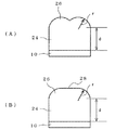
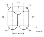
図6に示すように、略U字状の発光部の形状に対応し、直線部の各上面部分が半円柱状のシリンドリカルレンズ30,32,34と、半球状レンズ(正確には半球状レンズの一部分)36,38,40,42との組合せとなっている。半球状レンズ36,38は1/2部分よりなり、半球状レンズ40,42は1/4部分よりなる。上記の厚み方向のパラメータdのほか、図示するように、X軸方向に並置される一対のシリンドリカルレンズ30,32の中心間距離wが重要なパラメータである。
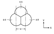
図7に示すように、略U字状発光部の形状に対応して、3個の半球状レンズ(正確には半球状レンズの一部分)44,46,48が、レンズ径より短い中心間距離で配列されて複合レンズを形成している。各半球状レンズは、扇形をしている。すなわち、2個の半球状レンズ46,48がX軸方向に並置され、これら2個の半球状レンズ46,48に接して、1個の半球状レンズ44が配置されている。U字状発光部の左右方向に対応する方向(X軸方向)の2つのレンズ46,48の中心間距離wが重要な形状パラメータである。
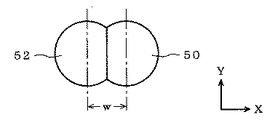
図8に示すように、略U字状の発光部の形状に対応し、単純に2個の半球状レンズ(正確には半球状レンズの一部分)50,52をレンズ径より短いレンズ中心間距離wでx軸方向に配列したものである。U字状発光部22の左右方向に対応する方向(X軸方向)の2つのレンズの中心間の方向(Y軸方向)が一致するように配置するが、その2つのレンズ中心間距離wが重要な形状パラメータである。

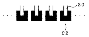
22 発光部
24 ベース部分
26 曲面部分
30,32,34 シリンドリカルレンズ
36,38,40,42,44,46,48,50,52 半球状レンズ
Claims (4)
- 複数の発光素子が1次元状に配列された発光素子アレイを構成するレンズ付き発光素子であって、
略U字状であって当該略U字状の一対の直線部が前記1次元の方向に並置された発光部を有する発光素子と、
前記発光部を覆うように前記発光素子上に設けられ、前記略U字状の発光部の前記一対の直線部を覆うように設けられた一対のシリンドリカルレンズと、当該一対の直線部の先端部を覆うように設けられた半球状レンズとを含む略U字状の複合レンズとを備え、
前記複合レンズは一定の厚みを有するベース部分と、その上部の表面に曲率を有する曲面部分とから構成され、
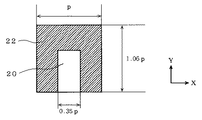
前記略U字状の発光部の、前記1次元の方向の幅をpとした場合に、
前記略U字状の発光部の前記一対の直線部の先端部の並置間隔は、0.35p、
前記複合レンズのベース部分の厚さは、0〜0.71p、
前記シリンドリカルレンズまたは半球状レンズの曲率半径は、0.20p〜0.47p、
前記一対のシリンドリカルレンズの中心間距離は0.70pである、レンズ付き発光素子。 - 前記複合レンズのベース部分の厚さは、0.35p、
前記シリンドリカルレンズまたは半球状レンズの曲率半径は、0.27pである、請求項1に記載のレンズ付き発光素子。 - 複数の発光素子が1次元状に配列された発光素子アレイを構成するレンズ付き発光素子であって、
略U字状であって当該略U字状の一対の直線部が前記1次元の方向に並置された発光部を有する発光素子と、
前記発光部を覆うように前記発光素子上に設けられ、前記略U字状の発光部の前記一対の直線部を覆うように設けられた前記1次元の方向に並置された2個の半球状レンズと、当該2個の半球状レンズに接する1個の半球状レンズとの組合わせよりなる複合レンズとを備え、
前記複合レンズは一定の厚みを有するベース部分と、その上部の表面に曲率を有する曲面部分とから構成され、
前記略U字状の発光部の、前記1次元の方向の幅をpとした場合に、
前記略U字状の発光部の前記一対の直線部の先端部の並置間隔は、0.35p、
前記複合レンズのベース部分の厚さは、0〜0.12p、
前記半球状レンズの曲率半径は、0.71p〜1.18p、
前記複合レンズを構成する3個の半球状レンズの相互の中心間距離は、1.41pである、レンズ付き発光素子。 - 前記複合レンズのベース部分の厚さは、0.12p、
前記半球状レンズの曲率半径は、0.94pである、請求項3に記載のレンズ付き発光素子。
Priority Applications (4)
| Application Number | Priority Date | Filing Date | Title |
|---|---|---|---|
| JP2004205508A JP4635494B2 (ja) | 2004-07-13 | 2004-07-13 | レンズ付き発光素子 |
| TW094122976A TW200607199A (en) | 2004-07-13 | 2005-07-07 | Lens-attached light-emitting element |
| CNB2005100833073A CN100435363C (zh) | 2004-07-13 | 2005-07-12 | 附带透镜的发光元件 |
| US11/180,217 US7142377B2 (en) | 2004-07-13 | 2005-07-13 | Lens-attached light-emitting element |
Applications Claiming Priority (1)
| Application Number | Priority Date | Filing Date | Title |
|---|---|---|---|
| JP2004205508A JP4635494B2 (ja) | 2004-07-13 | 2004-07-13 | レンズ付き発光素子 |
Publications (2)
| Publication Number | Publication Date |
|---|---|
| JP2006032448A JP2006032448A (ja) | 2006-02-02 |
| JP4635494B2 true JP4635494B2 (ja) | 2011-02-23 |
Family
ID=35599125
Family Applications (1)
| Application Number | Title | Priority Date | Filing Date |
|---|---|---|---|
| JP2004205508A Expired - Lifetime JP4635494B2 (ja) | 2004-07-13 | 2004-07-13 | レンズ付き発光素子 |
Country Status (4)
| Country | Link |
|---|---|
| US (1) | US7142377B2 (ja) |
| JP (1) | JP4635494B2 (ja) |
| CN (1) | CN100435363C (ja) |
| TW (1) | TW200607199A (ja) |
Families Citing this family (12)
| Publication number | Priority date | Publication date | Assignee | Title |
|---|---|---|---|---|
| JP4952028B2 (ja) * | 2006-04-04 | 2012-06-13 | 富士ゼロックス株式会社 | マイクロレンズ付き発光素子アレイチップ及び光書き込みヘッド |
| JP5157896B2 (ja) | 2006-04-04 | 2013-03-06 | 富士ゼロックス株式会社 | マイクロレンズ付き発光素子アレイ及び光書込みヘッド |
| CN102104705B (zh) * | 2009-12-21 | 2013-01-23 | 致伸科技股份有限公司 | 扫描装置及其发光结构 |
| KR101644140B1 (ko) * | 2010-01-07 | 2016-07-29 | 서울반도체 주식회사 | 비대칭 광 지향각 패턴을 갖는 led용 렌즈 및 그것을 포함하는 발광장치 |
| US8602605B2 (en) | 2010-01-07 | 2013-12-10 | Seoul Semiconductor Co., Ltd. | Aspherical LED lens and light emitting device including the same |
| JP5585292B2 (ja) * | 2010-08-16 | 2014-09-10 | 富士ゼロックス株式会社 | レンズ付発光素子アレイ及びプリントヘッド |
| CN104154463A (zh) * | 2010-09-27 | 2014-11-19 | 北京京东方光电科技有限公司 | 发光二极管光源及其制造方法、具有其的背光源 |
| JP5643720B2 (ja) * | 2011-06-30 | 2014-12-17 | 株式会社沖データ | ディスプレイモジュール及びその製造方法と表示装置 |
| JP5887767B2 (ja) * | 2011-08-31 | 2016-03-16 | 富士ゼロックス株式会社 | 発光部品、プリントヘッドおよび画像形成装置 |
| KR101887624B1 (ko) * | 2011-12-23 | 2018-08-13 | 서울반도체 주식회사 | 발광 모듈 및 렌즈 |
| US9123222B2 (en) | 2012-03-15 | 2015-09-01 | Ninve Jr. Inc. | Apparatus and method for detecting tampering with an infra-red motion sensor |
| US12360035B2 (en) * | 2020-10-12 | 2025-07-15 | Sony Group Corporation | Information processing apparatus, particle analysis apparatus, particle fractionation apparatus, and information processing method |
Family Cites Families (13)
| Publication number | Priority date | Publication date | Assignee | Title |
|---|---|---|---|---|
| US3844639A (en) * | 1972-12-11 | 1974-10-29 | Us Trad Corp | Converter lens |
| FR2554606B1 (fr) * | 1983-11-04 | 1987-04-10 | Thomson Csf | Dispositif optique de concentration du rayonnement lumineux emis par une diode electroluminescente, et diode electroluminescente comportant un tel dispositif |
| US5289082A (en) * | 1990-09-07 | 1994-02-22 | Kabushiki Kaisha Toshiba | LED lamp |
| US5526190A (en) * | 1994-09-29 | 1996-06-11 | Xerox Corporation | Optical element and device for providing uniform irradiance of a surface |
| JPH08156320A (ja) * | 1994-12-08 | 1996-06-18 | Matsushita Electric Ind Co Ltd | Ledプリンタヘッド及びその製造方法 |
| US5633527A (en) * | 1995-02-06 | 1997-05-27 | Sandia Corporation | Unitary lens semiconductor device |
| JPH09109455A (ja) | 1995-10-20 | 1997-04-28 | Ricoh Co Ltd | Ledアレイヘッド |
| JPH1127459A (ja) * | 1997-07-08 | 1999-01-29 | Ricoh Co Ltd | 画像形成装置 |
| US6188527B1 (en) * | 1999-04-12 | 2001-02-13 | Hewlett-Packard Company | LED array PCB with adhesive rod lens |
| JP2001036144A (ja) * | 1999-07-19 | 2001-02-09 | Stanley Electric Co Ltd | マイクロレンズ付発光素子アレイチップ及びその製造方法 |
| JP2002198571A (ja) * | 2000-12-26 | 2002-07-12 | Kyocera Corp | 半導体発光装置及びそれを用いた光プリンタヘッド |
| JP4140358B2 (ja) * | 2002-11-27 | 2008-08-27 | 富士ゼロックス株式会社 | 発光サイリスタ、発光サイリスタの製造方法および発光素子アレイチップ |
| WO2005001944A1 (ja) | 2003-06-26 | 2005-01-06 | Nippon Sheet Glass Company, Limited | レンズ付き発光素子およびその製造方法 |
-
2004
- 2004-07-13 JP JP2004205508A patent/JP4635494B2/ja not_active Expired - Lifetime
-
2005
- 2005-07-07 TW TW094122976A patent/TW200607199A/zh not_active IP Right Cessation
- 2005-07-12 CN CNB2005100833073A patent/CN100435363C/zh not_active Expired - Fee Related
- 2005-07-13 US US11/180,217 patent/US7142377B2/en not_active Expired - Fee Related
Also Published As
| Publication number | Publication date |
|---|---|
| CN100435363C (zh) | 2008-11-19 |
| TW200607199A (en) | 2006-02-16 |
| JP2006032448A (ja) | 2006-02-02 |
| US20060012888A1 (en) | 2006-01-19 |
| US7142377B2 (en) | 2006-11-28 |
| CN1722483A (zh) | 2006-01-18 |
| TWI358870B (ja) | 2012-02-21 |
Similar Documents
| Publication | Publication Date | Title |
|---|---|---|
| TWI392897B (zh) | 微型光學透鏡、含此透鏡之發光二極體封裝結構、及微型光學透鏡角度的設計方法 | |
| JP4093990B2 (ja) | 導光体、ライン照明装置および画像読取装置 | |
| US11302732B2 (en) | Array with light emitting diodes and varying lens | |
| JP4635494B2 (ja) | レンズ付き発光素子 | |
| US20040252522A1 (en) | Linear light source having indented reflecting plane | |
| JP2009303080A (ja) | 棒状導光体および画像読取装置 | |
| JP2012174601A (ja) | 照明装置 | |
| JP2017009778A (ja) | 照明用光学ユニット及び照明装置 | |
| JP6541450B2 (ja) | 照明装置 | |
| JP2006085150A (ja) | 発光装置のための光学システム | |
| JP5703180B2 (ja) | レンズ光学素子及び表示装置 | |
| JP6543825B2 (ja) | マイクロレンズアレイ | |
| JP7741999B1 (ja) | 光射出装置 | |
| JP2014010428A (ja) | ライン照明装置 | |
| JP4426250B2 (ja) | 入力結合装置 | |
| JP4423095B2 (ja) | 原稿照明装置、画像読み取り装置、カラー原稿読み取り装置、および画像形成装置 | |
| JP7216240B1 (ja) | 光学装置及びイメージセンサ | |
| EP3265862B1 (en) | Color correcting collimation of light from a color over position light source | |
| US20110235360A1 (en) | Light source device for supplying light to fiber optic illumination system | |
| JP4332190B2 (ja) | レーザラインジェネレータ及びレーザラインジェネレータモジュール | |
| JPS607425A (ja) | 発光素子 | |
| EP4610555A1 (en) | Lighting assembly for a vehicle | |
| JP6659240B2 (ja) | Led照明装置 | |
| JP7287668B2 (ja) | 照明装置 | |
| JPH10129033A (ja) | マルチビーム記録装置 |
Legal Events
| Date | Code | Title | Description |
|---|---|---|---|
| A711 | Notification of change in applicant |
Free format text: JAPANESE INTERMEDIATE CODE: A711 Effective date: 20070409 |
|
| RD03 | Notification of appointment of power of attorney |
Free format text: JAPANESE INTERMEDIATE CODE: A7423 Effective date: 20070409 |
|
| A521 | Request for written amendment filed |
Free format text: JAPANESE INTERMEDIATE CODE: A821 Effective date: 20070410 |
|
| A621 | Written request for application examination |
Free format text: JAPANESE INTERMEDIATE CODE: A621 Effective date: 20070531 |
|
| A977 | Report on retrieval |
Free format text: JAPANESE INTERMEDIATE CODE: A971007 Effective date: 20100212 |
|
| A131 | Notification of reasons for refusal |
Free format text: JAPANESE INTERMEDIATE CODE: A131 Effective date: 20100223 |
|
| A521 | Request for written amendment filed |
Free format text: JAPANESE INTERMEDIATE CODE: A523 Effective date: 20100421 |
|
| A131 | Notification of reasons for refusal |
Free format text: JAPANESE INTERMEDIATE CODE: A131 Effective date: 20100615 |
|
| A521 | Request for written amendment filed |
Free format text: JAPANESE INTERMEDIATE CODE: A523 Effective date: 20100810 |
|
| TRDD | Decision of grant or rejection written | ||
| A01 | Written decision to grant a patent or to grant a registration (utility model) |
Free format text: JAPANESE INTERMEDIATE CODE: A01 Effective date: 20101026 |
|
| A01 | Written decision to grant a patent or to grant a registration (utility model) |
Free format text: JAPANESE INTERMEDIATE CODE: A01 |
|
| A61 | First payment of annual fees (during grant procedure) |
Free format text: JAPANESE INTERMEDIATE CODE: A61 Effective date: 20101108 |
|
| FPAY | Renewal fee payment (event date is renewal date of database) |
Free format text: PAYMENT UNTIL: 20131203 Year of fee payment: 3 |
|
| R150 | Certificate of patent or registration of utility model |
Ref document number: 4635494 Country of ref document: JP Free format text: JAPANESE INTERMEDIATE CODE: R150 Free format text: JAPANESE INTERMEDIATE CODE: R150 |
|
| S533 | Written request for registration of change of name |
Free format text: JAPANESE INTERMEDIATE CODE: R313533 |
|
| R350 | Written notification of registration of transfer |
Free format text: JAPANESE INTERMEDIATE CODE: R350 |
|
| EXPY | Cancellation because of completion of term |