JP4635494B2 - Light emitting element with lens - Google Patents
Light emitting element with lens Download PDFInfo
- Publication number
- JP4635494B2 JP4635494B2 JP2004205508A JP2004205508A JP4635494B2 JP 4635494 B2 JP4635494 B2 JP 4635494B2 JP 2004205508 A JP2004205508 A JP 2004205508A JP 2004205508 A JP2004205508 A JP 2004205508A JP 4635494 B2 JP4635494 B2 JP 4635494B2
- Authority
- JP
- Japan
- Prior art keywords
- lens
- light emitting
- light
- emitting element
- shaped
- Prior art date
- Legal status (The legal status is an assumption and is not a legal conclusion. Google has not performed a legal analysis and makes no representation as to the accuracy of the status listed.)
- Expired - Lifetime
Links
Images


Classifications
-
- G—PHYSICS
- G02—OPTICS
- G02B—OPTICAL ELEMENTS, SYSTEMS OR APPARATUS
- G02B19/00—Condensers, e.g. light collectors or similar non-imaging optics
- G02B19/0033—Condensers, e.g. light collectors or similar non-imaging optics characterised by the use
- G02B19/0047—Condensers, e.g. light collectors or similar non-imaging optics characterised by the use for use with a light source
- G02B19/0061—Condensers, e.g. light collectors or similar non-imaging optics characterised by the use for use with a light source the light source comprising a LED
- G02B19/0066—Condensers, e.g. light collectors or similar non-imaging optics characterised by the use for use with a light source the light source comprising a LED in the form of an LED array
-
- G—PHYSICS
- G02—OPTICS
- G02B—OPTICAL ELEMENTS, SYSTEMS OR APPARATUS
- G02B19/00—Condensers, e.g. light collectors or similar non-imaging optics
- G02B19/0004—Condensers, e.g. light collectors or similar non-imaging optics characterised by the optical means employed
- G02B19/0009—Condensers, e.g. light collectors or similar non-imaging optics characterised by the optical means employed having refractive surfaces only
- G02B19/0014—Condensers, e.g. light collectors or similar non-imaging optics characterised by the optical means employed having refractive surfaces only at least one surface having optical power
-
- G—PHYSICS
- G02—OPTICS
- G02B—OPTICAL ELEMENTS, SYSTEMS OR APPARATUS
- G02B27/00—Optical systems or apparatus not provided for by any of the groups G02B1/00 - G02B26/00, G02B30/00
- G02B27/09—Beam shaping, e.g. changing the cross-sectional area, not otherwise provided for
- G02B27/0938—Using specific optical elements
- G02B27/095—Refractive optical elements
-
- H—ELECTRICITY
- H10—SEMICONDUCTOR DEVICES; ELECTRIC SOLID-STATE DEVICES NOT OTHERWISE PROVIDED FOR
- H10H—INORGANIC LIGHT-EMITTING SEMICONDUCTOR DEVICES HAVING POTENTIAL BARRIERS
- H10H20/00—Individual inorganic light-emitting semiconductor devices having potential barriers, e.g. light-emitting diodes [LED]
- H10H20/80—Constructional details
- H10H20/85—Packages
- H10H20/855—Optical field-shaping means, e.g. lenses
Landscapes
- Physics & Mathematics (AREA)
- General Physics & Mathematics (AREA)
- Optics & Photonics (AREA)
- Led Device Packages (AREA)
- Led Devices (AREA)
- Printers Or Recording Devices Using Electromagnetic And Radiation Means (AREA)
Description
本発明は、レンズ付き発光素子、特に光の取出し効率を向上させたレンズ付き発光素子に関する。 The present invention relates to a light-emitting element with a lens, and more particularly to a light-emitting element with a lens with improved light extraction efficiency.
光プリンタの書込みヘッドの光学系は、LEDアレイを構成する各LED素子の光点の像をレンズアレイにより感光ドラム上に結像させるように設計されている。レンズアレイには、屈折率分布型ロッドレンズアレイが用いられる場合が多い。 The optical system of the write head of the optical printer is designed so that the image of the light spot of each LED element constituting the LED array is formed on the photosensitive drum by the lens array. In many cases, a gradient index rod lens array is used as the lens array.
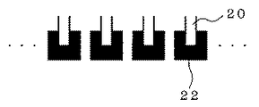
従来の光プリンタに用いられるLEDアレイ,屈折率分布型ロッドレンズアレイ,感光ドラムの代表的な構成例を図1に示す。10はLED、12はロッドレンズアレイ、14は感光ドラムである。
FIG. 1 shows a typical configuration example of an LED array, a gradient index rod lens array, and a photosensitive drum used in a conventional optical printer.
レンズアレイ12の実効的な口径角θが半角として17〜20゜であるのに対し、LED10は基本的にランバーシアン分布で発光しており、光の取出し効率は極めて低い。ランバーシアン分布で発光しているLEDの発光のうち、レンズアレイ12を介して感光ドラム14に伝達する光量は、およそ3〜5%に過ぎない。すなわち、LEDの発光量の95〜97%は利用できず、光取出し効率が低いという問題があった。
Whereas the effective aperture angle θ of the
光利用効率を高めるために、LED発光部の直上にマイクロレンズアレイを配置して、LED発光の指向性を少しでも狭めることによって、レンズアレイの口径角内に入射する光線を増やそうとすることが考えられる。しかしながら、一般に、光プリンタに使用されるLEDアレイの発光部は、図2に示されるように、電極20が発光部22の領域に突き出て、中央付近を塞いでしまっており、その結果、図2に示されるように、発光部22の領域の形状は略U字形の形状をしている。これを、図3に示すような一般的なマイクロレンズアレイ18で指向性を狭めようとする場合、破線23で示すレンズの光軸近傍の光線を利用するのが望ましいが、レンズの光軸近傍は、ちょうど電極20の位置に対応してしまい、その結果、十分に光取出し効率を向上できないという問題点がある。
In order to increase the efficiency of light utilization, a microlens array may be arranged immediately above the LED light emitting part to reduce the directivity of LED light emission as much as possible, thereby increasing the number of light rays incident on the aperture angle of the lens array. Conceivable. However, in general, as shown in FIG. 2, the light emitting portion of the LED array used in the optical printer has the
マイクロレンズアレイを備えたLEDアレイは、下記特許文献1,2,3に記載されているが、これら問題点は検討されておらず、したがってマイクロレンズの形状に関するものではない。 The LED array provided with the microlens array is described in the following Patent Documents 1, 2, and 3. However, these problems have not been studied, and thus are not related to the shape of the microlens.
以上のような問題は、LEDのみならず、その他の発光素子にもあてはまることである。
本発明の目的は、光の取出し効率を向上することのできるレンズ形状を提供することにある。 An object of the present invention is to provide a lens shape capable of improving the light extraction efficiency.
本発明の他の目的は、光取出し効率を向上させたレンズ付き発光素子を提供することにある。 Another object of the present invention is to provide a light-emitting element with a lens with improved light extraction efficiency.
本発明の第1の態様は、1次元状に配列された発光素子アレイを構成するレンズ付き発光素子であって、略U字状の発光部を有する発光素子と、前記発光素子上に設けられ、前記1次元の方向に並置された少なくとも2個のシリンドリカルレンズと、半球状レンズとの組合わせよりなる略U字状の複合レンズとを備え、前記複合レンズは一定の厚みを有するベース部分と、その上部の表面に曲率を有する曲面部分とから構成され、前記略U字状の発光部の、前記1次元の方向の幅をpとした場合に、前記複合レンズのベース部分の厚さは、0〜0.71p、前記シリンドリカルレンズまたは半球状レンズの曲率半径は、0.20p〜0.47p、前記少なくとも2個のシリンドリカルレンズの中心間距離は0.35p〜0.89pであることを特徴とする。 A first aspect of the present invention is a light-emitting element with a lens constituting a light-emitting element array arranged in a one-dimensional shape, the light-emitting element having a substantially U-shaped light-emitting portion, and provided on the light-emitting element. A substantially U-shaped compound lens composed of a combination of at least two cylindrical lenses juxtaposed in the one-dimensional direction and a hemispherical lens, and the compound lens has a base portion having a constant thickness; The base portion of the compound lens has a thickness when the width in the one-dimensional direction of the substantially U-shaped light-emitting portion is p. 0 to 0.71 p, the curvature radius of the cylindrical lens or hemispherical lens is 0.20 p to 0.47 p, and the distance between the centers of the at least two cylindrical lenses is 0.35 p to 0.89 p. And features.
本発明の第2の態様は、1次元状に配列された発光素子アレイを構成するレンズ付き発光素子であって、略U字状の発光部を有する発光素子と、前記発光素子上に設けられ、前記1次元の方向に並置された2個の半球状レンズと、1個の半球状レンズとの組合わせよりなる複合レンズとを備え、前記複合レンズは一定の厚みを有するベース部分と、その上部の表面に曲率を有する曲面部分とから構成され、前記略U字状の発光部の、前記1次元の方向の幅をpとした場合に、前記複合レンズのベース部分の厚さは、0〜0.71p、前記半球状レンズの曲率半径は、0.71p〜1.18p、前記2個の半球状レンズの中心間距離は、0.23p〜1.64pであることを特徴とする。 According to a second aspect of the present invention, there is provided a light emitting element with a lens constituting a light emitting element array arranged in a one-dimensional shape, the light emitting element having a substantially U-shaped light emitting portion, and provided on the light emitting element. , Two hemispherical lenses juxtaposed in the one-dimensional direction, and a compound lens formed by combining one hemispherical lens, the compound lens having a base portion having a certain thickness, and When the width in the one-dimensional direction of the substantially U-shaped light emitting portion is p, the thickness of the base portion of the compound lens is 0. The radius of curvature of the hemispherical lens is 0.71p to 1.18p, and the distance between the centers of the two hemispherical lenses is 0.23p to 1.64p.
本発明の第3の態様は、1次元状に配列された発光素子アレイを構成するレンズ付き発光素子であって、略U字状の発光部を有する発光素子と、前記発光素子上に設けられ、前記1次元の方向に並置された2個の半球状レンズの組合わせよりなる複合レンズとを備え、前記複合レンズは一定の厚みを有するベース部分と、その上部の表面に曲率を有する曲面部分とから構成され、前記略U字状の発光部の、前記1次元の方向の幅をpとした場合に、前記複合レンズのベース部分の厚さは、0〜0.71p、前記半球状レンズの曲率半径は、0.47p〜1.18p、前記2個の半球状レンズの中心間距離は、0.23p〜1.17pであることを特徴とする。 According to a third aspect of the present invention, there is provided a light emitting element with a lens constituting a one-dimensionally arranged light emitting element array, the light emitting element having a substantially U-shaped light emitting portion, and provided on the light emitting element. A compound lens comprising a combination of two hemispherical lenses juxtaposed in the one-dimensional direction, the compound lens having a base portion having a certain thickness and a curved surface portion having a curvature on the upper surface thereof The base portion of the compound lens has a thickness of 0 to 0.71 p, where p is the width in the one-dimensional direction of the substantially U-shaped light emitting portion. The curvature radius is 0.47p to 1.18p, and the distance between the centers of the two hemispherical lenses is 0.23p to 1.17p.
本発明によれば、光取出し効率を向上させたレンズ付き発光素子を実現できる。 ADVANTAGE OF THE INVENTION According to this invention, the light emitting element with a lens which improved the light extraction efficiency is realizable.
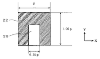
以下、本発明の実施例を図面に基づいて説明する。本発明のレンズ付き発光素子の一実施例は、図4に示すように、LEDの略U字形の発光部22上に複合レンズを設けたものである。発光部22は略U字形状を基本とし、図4のX軸方向の長さをpとして規格化する。このX軸方向は、この発光部をアレイとして使用する場合のアレイ方向、すなわち光点の走査方向となる。電極20の中心と、発光部22の中心とは、Y軸方向の線上にある。なお、X軸,Y軸はX−Y座標系の座標軸を示している。
Embodiments of the present invention will be described below with reference to the drawings. As shown in FIG. 4, one embodiment of the lens-equipped light-emitting element of the present invention is provided with a compound lens on a substantially U-shaped light-emitting
発光部22のY軸方向の長さは、1.06pであり、電極20の幅は、0.35pである。なお、これら値は、実施例で用いるモデルの値であり、限定的なものではない。
The length of the
以上のような略U字形発光部22上に設ける複合レンズの形状について説明する。なお、複合レンズは、樹脂で作製されるものとする。
The shape of the compound lens provided on the substantially U-shaped
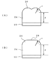
本発明の複合レンズの基本形状は、図5(A),(B)に示すように、LED10の発光部表面(発光面)から一定の厚みのベース部分24が存在し、その上に半球状または半円柱状の曲面部分26が存在する。図5(A)は、2つの曲面部分26が存在する場合を、図5(B)は、レンズ表面に曲面部分26の外に平坦部分28がある場合を、それぞれ示している。
As shown in FIGS. 5 (A) and 5 (B), the basic shape of the compound lens of the present invention is that a
上部曲面部分26の曲率半径を「曲率半径r」という。ただし図5(B)のようにレンズ表面に平坦部分が有る場合は、平坦部分以外の曲面部分の曲率半径を意味する。発光面から曲面の開始点までのベース部分の厚みを「ベース厚みd」というものとする。
The radius of curvature of the upper
以下、本発明の複合レンズの形状について説明する。 Hereinafter, the shape of the compound lens of the present invention will be described.
(a)略U字型複合レンズ
図6に示すように、略U字状の発光部の形状に対応し、直線部の各上面部分が半円柱状のシリンドリカルレンズ30,32,34と、半球状レンズ(正確には半球状レンズの一部分)36,38,40,42との組合せとなっている。半球状レンズ36,38は1/2部分よりなり、半球状レンズ40,42は1/4部分よりなる。上記の厚み方向のパラメータdのほか、図示するように、X軸方向に並置される一対のシリンドリカルレンズ30,32の中心間距離wが重要なパラメータである。
(A) Approximate U-shaped compound lens As shown in FIG. 6,
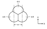
(b)3レンズ複合型
図7に示すように、略U字状発光部の形状に対応して、3個の半球状レンズ(正確には半球状レンズの一部分)44,46,48が、レンズ径より短い中心間距離で配列されて複合レンズを形成している。各半球状レンズは、扇形をしている。すなわち、2個の半球状レンズ46,48がX軸方向に並置され、これら2個の半球状レンズ46,48に接して、1個の半球状レンズ44が配置されている。U字状発光部の左右方向に対応する方向(X軸方向)の2つのレンズ46,48の中心間距離wが重要な形状パラメータである。
(B) Three-lens composite type As shown in FIG. 7, corresponding to the shape of the substantially U-shaped light-emitting portion, three hemispherical lenses (exactly part of the hemispherical lens) 44, 46, 48 are Arranged at a center-to-center distance shorter than the lens diameter to form a compound lens. Each hemispherical lens has a fan shape. That is, two
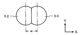
(c)2レンズ複合型
図8に示すように、略U字状の発光部の形状に対応し、単純に2個の半球状レンズ(正確には半球状レンズの一部分)50,52をレンズ径より短いレンズ中心間距離wでx軸方向に配列したものである。U字状発光部22の左右方向に対応する方向(X軸方向)の2つのレンズの中心間の方向(Y軸方向)が一致するように配置するが、その2つのレンズ中心間距離wが重要な形状パラメータである。
(C) Two-lens composite type As shown in FIG. 8, two hemispherical lenses (more precisely, a part of a hemispherical lens) 50 and 52 corresponding to the shape of a substantially U-shaped light-emitting portion are used as lenses. They are arranged in the x-axis direction at a lens center distance w shorter than the diameter. The U-shaped
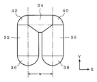
次に、レンズ形状の最適化について説明する。図4の発光部形状(実寸の例としてはp=17μmとした)に対し、曲率半径rとベース厚みdを各表に示すように2次元に変化させ、レンズがない場合に比べて光量が増加する(1.01倍以上となる)範囲を求めた。また光量が最大となるレンズ形状最適値を求めた。 Next, lens shape optimization will be described. For the shape of the light emitting portion of FIG. 4 (p = 17 μm as an actual size), the radius of curvature r and the base thickness d are changed two-dimensionally as shown in each table, and the amount of light is larger than when there is no lens. An increasing range (1.01 times or more) was determined. Also, the optimum lens shape value that maximizes the amount of light was obtained.
また、レンズ中心間距離wは、レンズの曲率半径rに対して発光部全面をレンズが覆うことができる範囲として決定した。発光部22上にレンズがない部分が生じると、光量低下を招くからである。
The lens center distance w is determined as a range in which the lens can cover the entire surface of the light emitting portion with respect to the curvature radius r of the lens. This is because if a portion without a lens is formed on the
一方、LEDアレイの発光部間のピッチは、発光部のX軸方向の長さpよりも小さくなることはない。上記の複合レンズを採用すれば、隣接レンズ間での干渉は起こらず、発光部間ピッチの変化は、光量増加に影響を与えない。実施例では発光部間ピッチは1.25pで計算した。 On the other hand, the pitch between the light emitting portions of the LED array does not become smaller than the length p in the X-axis direction of the light emitting portions. When the above compound lens is employed, no interference occurs between adjacent lenses, and the change in the pitch between the light emitting portions does not affect the increase in the amount of light. In the example, the pitch between the light emitting parts was calculated at 1.25 p.
まず、図6に示した略U字型複合レンズの場合について、説明する。 First, the case of the substantially U-shaped compound lens shown in FIG. 6 will be described.

ベース厚みdおよび曲率半径rを表1の範囲で変化させたときの光量と、レンズがない場合の光量との比(光量比)を測定した。測定結果を、表2に示す。光量比が1.01以上を、背景がグレー表示の領域内に示す。 The ratio (light quantity ratio) between the light quantity when the base thickness d and the curvature radius r were changed in the range of Table 1 and the light quantity when there was no lens was measured. The measurement results are shown in Table 2. A light amount ratio of 1.01 or more is shown in a gray display area.
最適条件のレンズ形状(曲率半径、ベース厚み)とレンズ中心間距離0.70p、樹脂屈折率1.55での光量は、レンズがない場合の2.1倍となった。なお、光量増加範囲内では、像の拡大は1.2倍以下であった。 The light quantity at the optimum lens shape (curvature radius, base thickness), the distance between the lens centers of 0.70 p, and the resin refractive index of 1.55 was 2.1 times that when there was no lens. It should be noted that the image magnification was 1.2 times or less within the light quantity increase range.
次に、図7に示した3レンズ型複合レンズの場合について説明する。 Next, the case of the three-lens type compound lens shown in FIG. 7 will be described.
ベース厚みdおよび曲率半径rを表3の範囲で変化させたときの光量比を測定する。測定結果を、表4に示す。光量比が1.01以上を、背景がグレー表示の領域内に示す。 The light quantity ratio is measured when the base thickness d and the curvature radius r are changed within the range shown in Table 3. The measurement results are shown in Table 4. A light amount ratio of 1.01 or more is shown in a gray display area.
最適条件のレンズ形状(曲率半径、ベース厚み)とレンズ中心間距離1.41p、樹脂屈折率1.55での光量は、レンズがない場合の1.1倍となった。なお、光量増加範囲内では、像の拡大は1.2倍以下であった。 The light quantity at the optimum lens shape (radius of curvature, base thickness), lens center distance 1.41p, and resin refractive index 1.55 was 1.1 times that without the lens. It should be noted that the image magnification was 1.2 times or less within the light quantity increase range.
次に、図8に示した2レンズ型複合レンズの場合について説明する。 Next, the case of the two-lens type compound lens shown in FIG. 8 will be described.
ベース厚みdおよび曲率半径rを表5の範囲で変化させたときの光量比を測定する。測定結果を、表6に示す。光量比が1.01以上を、背景がグレー表示の領域内に示す。 The light quantity ratio is measured when the base thickness d and the curvature radius r are changed within the ranges shown in Table 5. The measurement results are shown in Table 6. A light amount ratio of 1.01 or more is shown in a gray display area.
最適条件のレンズ形状(曲率半径、ベース厚み)とレンズ中心間距離0.94p、樹脂屈折率1.55での光量は、レンズがない場合の2.0倍となった。 The amount of light at the optimum lens shape (curvature radius, base thickness), distance between lens centers of 0.94 p, and resin refractive index of 1.55 was 2.0 times that without the lens.
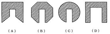
上記光量増加範囲は図4のような略U字形状の発光部を基本形状として求めたが、この発光部形状より発光部面積が相対的に縮小する場合においては、レンズ形状パラメータの上記各範囲内における明るさ比は1.01倍以上になる。したがって例えば図9に示すような形状の発光部の場合にも上記各数値範囲は有効である。 The light intensity increase range is obtained by using a substantially U-shaped light emitting portion as shown in FIG. 4 as a basic shape. However, when the light emitting portion area is relatively smaller than the light emitting portion shape, the above-mentioned ranges of lens shape parameters The brightness ratio inside is 1.01 or more. Therefore, for example, the above numerical ranges are also effective in the case of a light emitting portion having a shape as shown in FIG.
図9(A)は、図4のU字状発光部の両端を、斜め形状としたものである。図9(B)は、図4のU字状発光部の角部を、斜め形状としたものである。図9(C)は、図4のU字状発光部の外形を、円形状としたものである。図9(D)は、図4のU字状発光部を細くしたものである。 FIG. 9A shows an oblique shape at both ends of the U-shaped light emitting portion of FIG. FIG. 9B shows an example in which the corners of the U-shaped light-emitting portion in FIG. 4 are slanted. FIG. 9C shows a circular outer shape of the U-shaped light emitting portion of FIG. FIG. 9D shows a thinned U-shaped light emitting portion of FIG.
以上の各実施例では、発光素子として、LEDを例に説明したが、本発明はLEDに限定されるものではなく、他のあらゆる発光素子に適用できることは明らかである。発光素子の他の例としては、3端子発光サイリスタを挙げることができる。 In each of the above-described embodiments, the LED has been described as an example of the light emitting element. However, the present invention is not limited to the LED, and is obviously applicable to any other light emitting element. Another example of the light emitting element is a three-terminal light emitting thyristor.
20 電極
22 発光部
24 ベース部分
26 曲面部分
30,32,34 シリンドリカルレンズ
36,38,40,42,44,46,48,50,52 半球状レンズ
20
Claims (4)
略U字状であって当該略U字状の一対の直線部が前記1次元の方向に並置された発光部を有する発光素子と、
前記発光部を覆うように前記発光素子上に設けられ、前記略U字状の発光部の前記一対の直線部を覆うように設けられた一対のシリンドリカルレンズと、当該一対の直線部の先端部を覆うように設けられた半球状レンズとを含む略U字状の複合レンズとを備え、
前記複合レンズは一定の厚みを有するベース部分と、その上部の表面に曲率を有する曲面部分とから構成され、
前記略U字状の発光部の、前記1次元の方向の幅をpとした場合に、
前記略U字状の発光部の前記一対の直線部の先端部の並置間隔は、0.35p、
前記複合レンズのベース部分の厚さは、0〜0.71p、
前記シリンドリカルレンズまたは半球状レンズの曲率半径は、0.20p〜0.47p、
前記一対のシリンドリカルレンズの中心間距離は0.70pである、レンズ付き発光素子。 A light-emitting element with a lens constituting a light-emitting element array in which a plurality of light-emitting elements are arranged one-dimensionally,
A light emitting element having a light emitting portion that is substantially U-shaped and has a pair of substantially U-shaped linear portions juxtaposed in the one-dimensional direction;
A pair of cylindrical lenses provided on the light emitting element so as to cover the light emitting part and provided so as to cover the pair of linear parts of the substantially U-shaped light emitting part, and tip portions of the pair of linear parts A substantially U-shaped compound lens including a hemispherical lens provided so as to cover
The compound lens is composed of a base portion having a constant thickness and a curved surface portion having a curvature on the upper surface thereof,
When the width in the one-dimensional direction of the substantially U-shaped light emitting portion is p,
The juxtaposition interval between the tip portions of the pair of linear portions of the substantially U-shaped light emitting portion is 0.35 p,
The thickness of the base portion of the compound lens is 0 to 0.71p,
The curvature radius of the cylindrical lens or hemispherical lens is 0.20p to 0.47p,
A light emitting element with a lens, wherein a distance between centers of the pair of cylindrical lenses is 0.70 p.
前記シリンドリカルレンズまたは半球状レンズの曲率半径は、0.27pである、請求項1に記載のレンズ付き発光素子。 The thickness of the base portion of the compound lens is 0.35p,
The light emitting element with a lens according to claim 1, wherein a radius of curvature of the cylindrical lens or the hemispherical lens is 0.27p.
略U字状であって当該略U字状の一対の直線部が前記1次元の方向に並置された発光部を有する発光素子と、
前記発光部を覆うように前記発光素子上に設けられ、前記略U字状の発光部の前記一対の直線部を覆うように設けられた前記1次元の方向に並置された2個の半球状レンズと、当該2個の半球状レンズに接する1個の半球状レンズとの組合わせよりなる複合レンズとを備え、
前記複合レンズは一定の厚みを有するベース部分と、その上部の表面に曲率を有する曲面部分とから構成され、
前記略U字状の発光部の、前記1次元の方向の幅をpとした場合に、
前記略U字状の発光部の前記一対の直線部の先端部の並置間隔は、0.35p、
前記複合レンズのベース部分の厚さは、0〜0.12p、
前記半球状レンズの曲率半径は、0.71p〜1.18p、
前記複合レンズを構成する3個の半球状レンズの相互の中心間距離は、1.41pである、レンズ付き発光素子。 A light-emitting element with a lens constituting a light-emitting element array in which a plurality of light-emitting elements are arranged one-dimensionally,
A light emitting element having a light emitting portion that is substantially U-shaped and has a pair of substantially U-shaped linear portions juxtaposed in the one-dimensional direction;
Two hemispheres provided on the light emitting element so as to cover the light emitting part and juxtaposed in the one-dimensional direction provided so as to cover the pair of linear parts of the substantially U-shaped light emitting part A lens, and a compound lens formed by a combination of one hemispherical lens in contact with the two hemispherical lenses,
The compound lens is composed of a base portion having a constant thickness and a curved surface portion having a curvature on the upper surface thereof,
When the width in the one-dimensional direction of the substantially U-shaped light emitting portion is p,
The juxtaposition interval between the tip portions of the pair of linear portions of the substantially U-shaped light emitting portion is 0.35 p,
The thickness of the base portion of the compound lens is 0 to 0.12p,
The radius of curvature of the hemispherical lens is 0.71p to 1.18p,
The distance between centers of the three hemispherical lenses constituting the compound lens is 1.41p.
前記半球状レンズの曲率半径は、0.94pである、請求項3に記載のレンズ付き発光素子。 The thickness of the base portion of the compound lens is 0.12p,
The light emitting element with a lens according to claim 3, wherein a radius of curvature of the hemispherical lens is 0.94 p.
Priority Applications (4)
| Application Number | Priority Date | Filing Date | Title |
|---|---|---|---|
| JP2004205508A JP4635494B2 (en) | 2004-07-13 | 2004-07-13 | Light emitting element with lens |
| TW094122976A TW200607199A (en) | 2004-07-13 | 2005-07-07 | Lens-attached light-emitting element |
| CNB2005100833073A CN100435363C (en) | 2004-07-13 | 2005-07-12 | Light emitting element with lens |
| US11/180,217 US7142377B2 (en) | 2004-07-13 | 2005-07-13 | Lens-attached light-emitting element |
Applications Claiming Priority (1)
| Application Number | Priority Date | Filing Date | Title |
|---|---|---|---|
| JP2004205508A JP4635494B2 (en) | 2004-07-13 | 2004-07-13 | Light emitting element with lens |
Publications (2)
| Publication Number | Publication Date |
|---|---|
| JP2006032448A JP2006032448A (en) | 2006-02-02 |
| JP4635494B2 true JP4635494B2 (en) | 2011-02-23 |
Family
ID=35599125
Family Applications (1)
| Application Number | Title | Priority Date | Filing Date |
|---|---|---|---|
| JP2004205508A Expired - Lifetime JP4635494B2 (en) | 2004-07-13 | 2004-07-13 | Light emitting element with lens |
Country Status (4)
| Country | Link |
|---|---|
| US (1) | US7142377B2 (en) |
| JP (1) | JP4635494B2 (en) |
| CN (1) | CN100435363C (en) |
| TW (1) | TW200607199A (en) |
Families Citing this family (12)
| Publication number | Priority date | Publication date | Assignee | Title |
|---|---|---|---|---|
| US8089077B2 (en) | 2006-04-04 | 2012-01-03 | Fuji Xerox Co., Ltd. | Light-emitting element array with micro-lenses and optical writing head |
| JP4952028B2 (en) * | 2006-04-04 | 2012-06-13 | 富士ゼロックス株式会社 | Light emitting element array chip with microlens and optical writing head |
| CN102104705B (en) * | 2009-12-21 | 2013-01-23 | 致伸科技股份有限公司 | Scanning device and its light emitting structure |
| KR101644140B1 (en) * | 2010-01-07 | 2016-07-29 | 서울반도체 주식회사 | Led lens having an asymmetric orientation angle pattern and light emitting device having the same |
| US8602605B2 (en) | 2010-01-07 | 2013-12-10 | Seoul Semiconductor Co., Ltd. | Aspherical LED lens and light emitting device including the same |
| JP5585292B2 (en) * | 2010-08-16 | 2014-09-10 | 富士ゼロックス株式会社 | Light emitting element array with lens and print head |
| CN104154463A (en) * | 2010-09-27 | 2014-11-19 | 北京京东方光电科技有限公司 | Light emitting diode source and manufacturing method thereof and backlight source with light emitting diode source |
| JP5643720B2 (en) * | 2011-06-30 | 2014-12-17 | 株式会社沖データ | Display module, manufacturing method thereof and display device |
| JP5887767B2 (en) * | 2011-08-31 | 2016-03-16 | 富士ゼロックス株式会社 | Light emitting component, print head, and image forming apparatus |
| KR101887624B1 (en) * | 2011-12-23 | 2018-08-13 | 서울반도체 주식회사 | Light emitting module and lens |
| US9123222B2 (en) | 2012-03-15 | 2015-09-01 | Ninve Jr. Inc. | Apparatus and method for detecting tampering with an infra-red motion sensor |
| US12360035B2 (en) * | 2020-10-12 | 2025-07-15 | Sony Group Corporation | Information processing apparatus, particle analysis apparatus, particle fractionation apparatus, and information processing method |
Family Cites Families (13)
| Publication number | Priority date | Publication date | Assignee | Title |
|---|---|---|---|---|
| US3844639A (en) * | 1972-12-11 | 1974-10-29 | Us Trad Corp | Converter lens |
| FR2554606B1 (en) * | 1983-11-04 | 1987-04-10 | Thomson Csf | OPTICAL DEVICE FOR CONCENTRATION OF LIGHT RADIATION EMITTED BY A LIGHT EMITTING DIODE, AND LIGHT EMITTING DIODE COMPRISING SUCH A DEVICE |
| US5289082A (en) * | 1990-09-07 | 1994-02-22 | Kabushiki Kaisha Toshiba | LED lamp |
| US5526190A (en) * | 1994-09-29 | 1996-06-11 | Xerox Corporation | Optical element and device for providing uniform irradiance of a surface |
| JPH08156320A (en) * | 1994-12-08 | 1996-06-18 | Matsushita Electric Ind Co Ltd | LED printer head and manufacturing method thereof |
| US5633527A (en) * | 1995-02-06 | 1997-05-27 | Sandia Corporation | Unitary lens semiconductor device |
| JPH09109455A (en) | 1995-10-20 | 1997-04-28 | Ricoh Co Ltd | LED array head |
| JPH1127459A (en) * | 1997-07-08 | 1999-01-29 | Ricoh Co Ltd | Image forming device |
| US6188527B1 (en) * | 1999-04-12 | 2001-02-13 | Hewlett-Packard Company | LED array PCB with adhesive rod lens |
| JP2001036144A (en) * | 1999-07-19 | 2001-02-09 | Stanley Electric Co Ltd | Light emitting element array chip with microlens and method of manufacturing the same |
| JP2002198571A (en) * | 2000-12-26 | 2002-07-12 | Kyocera Corp | Semiconductor light emitting device and optical printer head using the same |
| JP4140358B2 (en) * | 2002-11-27 | 2008-08-27 | 富士ゼロックス株式会社 | Light emitting thyristor, light emitting thyristor manufacturing method, and light emitting element array chip |
| WO2005001944A1 (en) | 2003-06-26 | 2005-01-06 | Nippon Sheet Glass Company, Limited | Lens-carrying light emitting element and production method therefor |
-
2004
- 2004-07-13 JP JP2004205508A patent/JP4635494B2/en not_active Expired - Lifetime
-
2005
- 2005-07-07 TW TW094122976A patent/TW200607199A/en not_active IP Right Cessation
- 2005-07-12 CN CNB2005100833073A patent/CN100435363C/en not_active Expired - Fee Related
- 2005-07-13 US US11/180,217 patent/US7142377B2/en not_active Expired - Fee Related
Also Published As
| Publication number | Publication date |
|---|---|
| US20060012888A1 (en) | 2006-01-19 |
| CN1722483A (en) | 2006-01-18 |
| TW200607199A (en) | 2006-02-16 |
| TWI358870B (en) | 2012-02-21 |
| JP2006032448A (en) | 2006-02-02 |
| US7142377B2 (en) | 2006-11-28 |
| CN100435363C (en) | 2008-11-19 |
Similar Documents
| Publication | Publication Date | Title |
|---|---|---|
| JP4093990B2 (en) | Light guide, line illumination device, and image reading device | |
| US11302732B2 (en) | Array with light emitting diodes and varying lens | |
| JP4635494B2 (en) | Light emitting element with lens | |
| JP5100278B2 (en) | Light guiding optical system, document illumination device using the same, and image reading device using the same | |
| US7914174B2 (en) | Method to optimize micro-optic lens in LED flashlight application | |
| JP2012174601A (en) | Lighting device | |
| JP2009303080A (en) | Rod-shaped light guide and image reading apparatus | |
| JP6541450B2 (en) | Lighting device | |
| JP5018192B2 (en) | Lighting device | |
| JP2006085150A (en) | Optical system for light emitting apparatus | |
| JP6543825B2 (en) | Micro lens array | |
| US20140300972A1 (en) | Lens optical element and display apparatus | |
| JP2014010428A (en) | Line illumination apparatus | |
| JP4426250B2 (en) | Input coupling device | |
| JP2019079765A (en) | Line light source and optical line sensor unit provided with the same | |
| JP4423095B2 (en) | Document illumination device, image reading device, color document reading device, and image forming device | |
| EP3265862B1 (en) | Color correcting collimation of light from a color over position light source | |
| JP2013161734A (en) | Lighting device having a plurality of light sources | |
| US20110235360A1 (en) | Light source device for supplying light to fiber optic illumination system | |
| JP4332190B2 (en) | Laser line generator and laser line generator module | |
| JPS607425A (en) | light emitting element | |
| JP7216240B1 (en) | Optical devices and image sensors | |
| EP4610555A1 (en) | Lighting assembly for a vehicle | |
| JPH10129033A (en) | Multi-beam recorder | |
| JP2017116701A5 (en) |
Legal Events
| Date | Code | Title | Description |
|---|---|---|---|
| A711 | Notification of change in applicant |
Free format text: JAPANESE INTERMEDIATE CODE: A711 Effective date: 20070409 |
|
| RD03 | Notification of appointment of power of attorney |
Free format text: JAPANESE INTERMEDIATE CODE: A7423 Effective date: 20070409 |
|
| A521 | Request for written amendment filed |
Free format text: JAPANESE INTERMEDIATE CODE: A821 Effective date: 20070410 |
|
| A621 | Written request for application examination |
Free format text: JAPANESE INTERMEDIATE CODE: A621 Effective date: 20070531 |
|
| A977 | Report on retrieval |
Free format text: JAPANESE INTERMEDIATE CODE: A971007 Effective date: 20100212 |
|
| A131 | Notification of reasons for refusal |
Free format text: JAPANESE INTERMEDIATE CODE: A131 Effective date: 20100223 |
|
| A521 | Request for written amendment filed |
Free format text: JAPANESE INTERMEDIATE CODE: A523 Effective date: 20100421 |
|
| A131 | Notification of reasons for refusal |
Free format text: JAPANESE INTERMEDIATE CODE: A131 Effective date: 20100615 |
|
| A521 | Request for written amendment filed |
Free format text: JAPANESE INTERMEDIATE CODE: A523 Effective date: 20100810 |
|
| TRDD | Decision of grant or rejection written | ||
| A01 | Written decision to grant a patent or to grant a registration (utility model) |
Free format text: JAPANESE INTERMEDIATE CODE: A01 Effective date: 20101026 |
|
| A01 | Written decision to grant a patent or to grant a registration (utility model) |
Free format text: JAPANESE INTERMEDIATE CODE: A01 |
|
| A61 | First payment of annual fees (during grant procedure) |
Free format text: JAPANESE INTERMEDIATE CODE: A61 Effective date: 20101108 |
|
| FPAY | Renewal fee payment (event date is renewal date of database) |
Free format text: PAYMENT UNTIL: 20131203 Year of fee payment: 3 |
|
| R150 | Certificate of patent or registration of utility model |
Ref document number: 4635494 Country of ref document: JP Free format text: JAPANESE INTERMEDIATE CODE: R150 Free format text: JAPANESE INTERMEDIATE CODE: R150 |
|
| S533 | Written request for registration of change of name |
Free format text: JAPANESE INTERMEDIATE CODE: R313533 |
|
| R350 | Written notification of registration of transfer |
Free format text: JAPANESE INTERMEDIATE CODE: R350 |
|
| EXPY | Cancellation because of completion of term |