JP3826605B2 - 半導体装置の実装構造の製造方法、液晶装置、および電子機器 - Google Patents
半導体装置の実装構造の製造方法、液晶装置、および電子機器 Download PDFInfo
- Publication number
- JP3826605B2 JP3826605B2 JP06045999A JP6045999A JP3826605B2 JP 3826605 B2 JP3826605 B2 JP 3826605B2 JP 06045999 A JP06045999 A JP 06045999A JP 6045999 A JP6045999 A JP 6045999A JP 3826605 B2 JP3826605 B2 JP 3826605B2
- Authority
- JP
- Japan
- Prior art keywords
- liquid crystal
- electrode
- substrate
- bump
- crystal device
- Prior art date
- Legal status (The legal status is an assumption and is not a legal conclusion. Google has not performed a legal analysis and makes no representation as to the accuracy of the status listed.)
- Expired - Lifetime
Links
Images


Classifications
-
- H—ELECTRICITY
- H01—ELECTRIC ELEMENTS
- H01L—SEMICONDUCTOR DEVICES NOT COVERED BY CLASS H10
- H01L24/00—Arrangements for connecting or disconnecting semiconductor or solid-state bodies; Methods or apparatus related thereto
- H01L24/01—Means for bonding being attached to, or being formed on, the surface to be connected, e.g. chip-to-package, die-attach, "first-level" interconnects; Manufacturing methods related thereto
- H01L24/10—Bump connectors ; Manufacturing methods related thereto
- H01L24/12—Structure, shape, material or disposition of the bump connectors prior to the connecting process
- H01L24/13—Structure, shape, material or disposition of the bump connectors prior to the connecting process of an individual bump connector
-
- H—ELECTRICITY
- H01—ELECTRIC ELEMENTS
- H01L—SEMICONDUCTOR DEVICES NOT COVERED BY CLASS H10
- H01L24/00—Arrangements for connecting or disconnecting semiconductor or solid-state bodies; Methods or apparatus related thereto
- H01L24/01—Means for bonding being attached to, or being formed on, the surface to be connected, e.g. chip-to-package, die-attach, "first-level" interconnects; Manufacturing methods related thereto
- H01L24/10—Bump connectors ; Manufacturing methods related thereto
- H01L24/11—Manufacturing methods
-
- H—ELECTRICITY
- H01—ELECTRIC ELEMENTS
- H01L—SEMICONDUCTOR DEVICES NOT COVERED BY CLASS H10
- H01L24/00—Arrangements for connecting or disconnecting semiconductor or solid-state bodies; Methods or apparatus related thereto
- H01L24/01—Means for bonding being attached to, or being formed on, the surface to be connected, e.g. chip-to-package, die-attach, "first-level" interconnects; Manufacturing methods related thereto
- H01L24/26—Layer connectors, e.g. plate connectors, solder or adhesive layers; Manufacturing methods related thereto
- H01L24/28—Structure, shape, material or disposition of the layer connectors prior to the connecting process
- H01L24/29—Structure, shape, material or disposition of the layer connectors prior to the connecting process of an individual layer connector
-
- H—ELECTRICITY
- H01—ELECTRIC ELEMENTS
- H01L—SEMICONDUCTOR DEVICES NOT COVERED BY CLASS H10
- H01L24/00—Arrangements for connecting or disconnecting semiconductor or solid-state bodies; Methods or apparatus related thereto
- H01L24/80—Methods for connecting semiconductor or other solid state bodies using means for bonding being attached to, or being formed on, the surface to be connected
- H01L24/83—Methods for connecting semiconductor or other solid state bodies using means for bonding being attached to, or being formed on, the surface to be connected using a layer connector
-
- G—PHYSICS
- G02—OPTICS
- G02F—OPTICAL DEVICES OR ARRANGEMENTS FOR THE CONTROL OF LIGHT BY MODIFICATION OF THE OPTICAL PROPERTIES OF THE MEDIA OF THE ELEMENTS INVOLVED THEREIN; NON-LINEAR OPTICS; FREQUENCY-CHANGING OF LIGHT; OPTICAL LOGIC ELEMENTS; OPTICAL ANALOGUE/DIGITAL CONVERTERS
- G02F1/00—Devices or arrangements for the control of the intensity, colour, phase, polarisation or direction of light arriving from an independent light source, e.g. switching, gating or modulating; Non-linear optics
- G02F1/01—Devices or arrangements for the control of the intensity, colour, phase, polarisation or direction of light arriving from an independent light source, e.g. switching, gating or modulating; Non-linear optics for the control of the intensity, phase, polarisation or colour
- G02F1/13—Devices or arrangements for the control of the intensity, colour, phase, polarisation or direction of light arriving from an independent light source, e.g. switching, gating or modulating; Non-linear optics for the control of the intensity, phase, polarisation or colour based on liquid crystals, e.g. single liquid crystal display cells
- G02F1/133—Constructional arrangements; Operation of liquid crystal cells; Circuit arrangements
- G02F1/1333—Constructional arrangements; Manufacturing methods
- G02F1/1345—Conductors connecting electrodes to cell terminals
- G02F1/13452—Conductors connecting driver circuitry and terminals of panels
-
- H—ELECTRICITY
- H01—ELECTRIC ELEMENTS
- H01L—SEMICONDUCTOR DEVICES NOT COVERED BY CLASS H10
- H01L2224/00—Indexing scheme for arrangements for connecting or disconnecting semiconductor or solid-state bodies and methods related thereto as covered by H01L24/00
- H01L2224/01—Means for bonding being attached to, or being formed on, the surface to be connected, e.g. chip-to-package, die-attach, "first-level" interconnects; Manufacturing methods related thereto
- H01L2224/02—Bonding areas; Manufacturing methods related thereto
- H01L2224/04—Structure, shape, material or disposition of the bonding areas prior to the connecting process
- H01L2224/05—Structure, shape, material or disposition of the bonding areas prior to the connecting process of an individual bonding area
- H01L2224/0554—External layer
- H01L2224/0556—Disposition
- H01L2224/05571—Disposition the external layer being disposed in a recess of the surface
-
- H—ELECTRICITY
- H01—ELECTRIC ELEMENTS
- H01L—SEMICONDUCTOR DEVICES NOT COVERED BY CLASS H10
- H01L2224/00—Indexing scheme for arrangements for connecting or disconnecting semiconductor or solid-state bodies and methods related thereto as covered by H01L24/00
- H01L2224/01—Means for bonding being attached to, or being formed on, the surface to be connected, e.g. chip-to-package, die-attach, "first-level" interconnects; Manufacturing methods related thereto
- H01L2224/02—Bonding areas; Manufacturing methods related thereto
- H01L2224/04—Structure, shape, material or disposition of the bonding areas prior to the connecting process
- H01L2224/05—Structure, shape, material or disposition of the bonding areas prior to the connecting process of an individual bonding area
- H01L2224/0554—External layer
- H01L2224/05573—Single external layer
-
- H—ELECTRICITY
- H01—ELECTRIC ELEMENTS
- H01L—SEMICONDUCTOR DEVICES NOT COVERED BY CLASS H10
- H01L2224/00—Indexing scheme for arrangements for connecting or disconnecting semiconductor or solid-state bodies and methods related thereto as covered by H01L24/00
- H01L2224/01—Means for bonding being attached to, or being formed on, the surface to be connected, e.g. chip-to-package, die-attach, "first-level" interconnects; Manufacturing methods related thereto
- H01L2224/10—Bump connectors; Manufacturing methods related thereto
- H01L2224/11—Manufacturing methods
- H01L2224/1147—Manufacturing methods using a lift-off mask
-
- H—ELECTRICITY
- H01—ELECTRIC ELEMENTS
- H01L—SEMICONDUCTOR DEVICES NOT COVERED BY CLASS H10
- H01L2224/00—Indexing scheme for arrangements for connecting or disconnecting semiconductor or solid-state bodies and methods related thereto as covered by H01L24/00
- H01L2224/01—Means for bonding being attached to, or being formed on, the surface to be connected, e.g. chip-to-package, die-attach, "first-level" interconnects; Manufacturing methods related thereto
- H01L2224/10—Bump connectors; Manufacturing methods related thereto
- H01L2224/12—Structure, shape, material or disposition of the bump connectors prior to the connecting process
- H01L2224/13—Structure, shape, material or disposition of the bump connectors prior to the connecting process of an individual bump connector
- H01L2224/13001—Core members of the bump connector
- H01L2224/1301—Shape
- H01L2224/13016—Shape in side view
- H01L2224/13017—Shape in side view being non uniform along the bump connector
-
- H—ELECTRICITY
- H01—ELECTRIC ELEMENTS
- H01L—SEMICONDUCTOR DEVICES NOT COVERED BY CLASS H10
- H01L2224/00—Indexing scheme for arrangements for connecting or disconnecting semiconductor or solid-state bodies and methods related thereto as covered by H01L24/00
- H01L2224/01—Means for bonding being attached to, or being formed on, the surface to be connected, e.g. chip-to-package, die-attach, "first-level" interconnects; Manufacturing methods related thereto
- H01L2224/10—Bump connectors; Manufacturing methods related thereto
- H01L2224/12—Structure, shape, material or disposition of the bump connectors prior to the connecting process
- H01L2224/13—Structure, shape, material or disposition of the bump connectors prior to the connecting process of an individual bump connector
- H01L2224/13001—Core members of the bump connector
- H01L2224/13099—Material
-
- H—ELECTRICITY
- H01—ELECTRIC ELEMENTS
- H01L—SEMICONDUCTOR DEVICES NOT COVERED BY CLASS H10
- H01L2224/00—Indexing scheme for arrangements for connecting or disconnecting semiconductor or solid-state bodies and methods related thereto as covered by H01L24/00
- H01L2224/01—Means for bonding being attached to, or being formed on, the surface to be connected, e.g. chip-to-package, die-attach, "first-level" interconnects; Manufacturing methods related thereto
- H01L2224/10—Bump connectors; Manufacturing methods related thereto
- H01L2224/15—Structure, shape, material or disposition of the bump connectors after the connecting process
- H01L2224/16—Structure, shape, material or disposition of the bump connectors after the connecting process of an individual bump connector
-
- H—ELECTRICITY
- H01—ELECTRIC ELEMENTS
- H01L—SEMICONDUCTOR DEVICES NOT COVERED BY CLASS H10
- H01L2224/00—Indexing scheme for arrangements for connecting or disconnecting semiconductor or solid-state bodies and methods related thereto as covered by H01L24/00
- H01L2224/73—Means for bonding being of different types provided for in two or more of groups H01L2224/10, H01L2224/18, H01L2224/26, H01L2224/34, H01L2224/42, H01L2224/50, H01L2224/63, H01L2224/71
- H01L2224/732—Location after the connecting process
- H01L2224/73201—Location after the connecting process on the same surface
- H01L2224/73203—Bump and layer connectors
- H01L2224/73204—Bump and layer connectors the bump connector being embedded into the layer connector
-
- H—ELECTRICITY
- H01—ELECTRIC ELEMENTS
- H01L—SEMICONDUCTOR DEVICES NOT COVERED BY CLASS H10
- H01L2224/00—Indexing scheme for arrangements for connecting or disconnecting semiconductor or solid-state bodies and methods related thereto as covered by H01L24/00
- H01L2224/80—Methods for connecting semiconductor or other solid state bodies using means for bonding being attached to, or being formed on, the surface to be connected
- H01L2224/83—Methods for connecting semiconductor or other solid state bodies using means for bonding being attached to, or being formed on, the surface to be connected using a layer connector
- H01L2224/831—Methods for connecting semiconductor or other solid state bodies using means for bonding being attached to, or being formed on, the surface to be connected using a layer connector the layer connector being supplied to the parts to be connected in the bonding apparatus
- H01L2224/83101—Methods for connecting semiconductor or other solid state bodies using means for bonding being attached to, or being formed on, the surface to be connected using a layer connector the layer connector being supplied to the parts to be connected in the bonding apparatus as prepeg comprising a layer connector, e.g. provided in an insulating plate member
-
- H—ELECTRICITY
- H01—ELECTRIC ELEMENTS
- H01L—SEMICONDUCTOR DEVICES NOT COVERED BY CLASS H10
- H01L2224/00—Indexing scheme for arrangements for connecting or disconnecting semiconductor or solid-state bodies and methods related thereto as covered by H01L24/00
- H01L2224/80—Methods for connecting semiconductor or other solid state bodies using means for bonding being attached to, or being formed on, the surface to be connected
- H01L2224/83—Methods for connecting semiconductor or other solid state bodies using means for bonding being attached to, or being formed on, the surface to be connected using a layer connector
- H01L2224/8319—Arrangement of the layer connectors prior to mounting
-
- H—ELECTRICITY
- H01—ELECTRIC ELEMENTS
- H01L—SEMICONDUCTOR DEVICES NOT COVERED BY CLASS H10
- H01L2224/00—Indexing scheme for arrangements for connecting or disconnecting semiconductor or solid-state bodies and methods related thereto as covered by H01L24/00
- H01L2224/80—Methods for connecting semiconductor or other solid state bodies using means for bonding being attached to, or being formed on, the surface to be connected
- H01L2224/83—Methods for connecting semiconductor or other solid state bodies using means for bonding being attached to, or being formed on, the surface to be connected using a layer connector
- H01L2224/838—Bonding techniques
-
- H—ELECTRICITY
- H01—ELECTRIC ELEMENTS
- H01L—SEMICONDUCTOR DEVICES NOT COVERED BY CLASS H10
- H01L23/00—Details of semiconductor or other solid state devices
- H01L23/48—Arrangements for conducting electric current to or from the solid state body in operation, e.g. leads, terminal arrangements ; Selection of materials therefor
- H01L23/488—Arrangements for conducting electric current to or from the solid state body in operation, e.g. leads, terminal arrangements ; Selection of materials therefor consisting of soldered or bonded constructions
- H01L23/498—Leads, i.e. metallisations or lead-frames on insulating substrates, e.g. chip carriers
- H01L23/49811—Additional leads joined to the metallisation on the insulating substrate, e.g. pins, bumps, wires, flat leads
-
- H—ELECTRICITY
- H01—ELECTRIC ELEMENTS
- H01L—SEMICONDUCTOR DEVICES NOT COVERED BY CLASS H10
- H01L2924/00—Indexing scheme for arrangements or methods for connecting or disconnecting semiconductor or solid-state bodies as covered by H01L24/00
- H01L2924/0001—Technical content checked by a classifier
- H01L2924/00014—Technical content checked by a classifier the subject-matter covered by the group, the symbol of which is combined with the symbol of this group, being disclosed without further technical details
-
- H—ELECTRICITY
- H01—ELECTRIC ELEMENTS
- H01L—SEMICONDUCTOR DEVICES NOT COVERED BY CLASS H10
- H01L2924/00—Indexing scheme for arrangements or methods for connecting or disconnecting semiconductor or solid-state bodies as covered by H01L24/00
- H01L2924/01—Chemical elements
- H01L2924/01004—Beryllium [Be]
-
- H—ELECTRICITY
- H01—ELECTRIC ELEMENTS
- H01L—SEMICONDUCTOR DEVICES NOT COVERED BY CLASS H10
- H01L2924/00—Indexing scheme for arrangements or methods for connecting or disconnecting semiconductor or solid-state bodies as covered by H01L24/00
- H01L2924/01—Chemical elements
- H01L2924/01005—Boron [B]
-
- H—ELECTRICITY
- H01—ELECTRIC ELEMENTS
- H01L—SEMICONDUCTOR DEVICES NOT COVERED BY CLASS H10
- H01L2924/00—Indexing scheme for arrangements or methods for connecting or disconnecting semiconductor or solid-state bodies as covered by H01L24/00
- H01L2924/01—Chemical elements
- H01L2924/01006—Carbon [C]
-
- H—ELECTRICITY
- H01—ELECTRIC ELEMENTS
- H01L—SEMICONDUCTOR DEVICES NOT COVERED BY CLASS H10
- H01L2924/00—Indexing scheme for arrangements or methods for connecting or disconnecting semiconductor or solid-state bodies as covered by H01L24/00
- H01L2924/01—Chemical elements
- H01L2924/01033—Arsenic [As]
-
- H—ELECTRICITY
- H01—ELECTRIC ELEMENTS
- H01L—SEMICONDUCTOR DEVICES NOT COVERED BY CLASS H10
- H01L2924/00—Indexing scheme for arrangements or methods for connecting or disconnecting semiconductor or solid-state bodies as covered by H01L24/00
- H01L2924/01—Chemical elements
- H01L2924/01049—Indium [In]
-
- H—ELECTRICITY
- H01—ELECTRIC ELEMENTS
- H01L—SEMICONDUCTOR DEVICES NOT COVERED BY CLASS H10
- H01L2924/00—Indexing scheme for arrangements or methods for connecting or disconnecting semiconductor or solid-state bodies as covered by H01L24/00
- H01L2924/01—Chemical elements
- H01L2924/0105—Tin [Sn]
-
- H—ELECTRICITY
- H01—ELECTRIC ELEMENTS
- H01L—SEMICONDUCTOR DEVICES NOT COVERED BY CLASS H10
- H01L2924/00—Indexing scheme for arrangements or methods for connecting or disconnecting semiconductor or solid-state bodies as covered by H01L24/00
- H01L2924/01—Chemical elements
- H01L2924/01078—Platinum [Pt]
-
- H—ELECTRICITY
- H01—ELECTRIC ELEMENTS
- H01L—SEMICONDUCTOR DEVICES NOT COVERED BY CLASS H10
- H01L2924/00—Indexing scheme for arrangements or methods for connecting or disconnecting semiconductor or solid-state bodies as covered by H01L24/00
- H01L2924/01—Chemical elements
- H01L2924/01082—Lead [Pb]
-
- H—ELECTRICITY
- H01—ELECTRIC ELEMENTS
- H01L—SEMICONDUCTOR DEVICES NOT COVERED BY CLASS H10
- H01L2924/00—Indexing scheme for arrangements or methods for connecting or disconnecting semiconductor or solid-state bodies as covered by H01L24/00
- H01L2924/06—Polymers
- H01L2924/078—Adhesive characteristics other than chemical
- H01L2924/0781—Adhesive characteristics other than chemical being an ohmic electrical conductor
-
- H—ELECTRICITY
- H01—ELECTRIC ELEMENTS
- H01L—SEMICONDUCTOR DEVICES NOT COVERED BY CLASS H10
- H01L2924/00—Indexing scheme for arrangements or methods for connecting or disconnecting semiconductor or solid-state bodies as covered by H01L24/00
- H01L2924/10—Details of semiconductor or other solid state devices to be connected
- H01L2924/11—Device type
- H01L2924/14—Integrated circuits
-
- H—ELECTRICITY
- H01—ELECTRIC ELEMENTS
- H01L—SEMICONDUCTOR DEVICES NOT COVERED BY CLASS H10
- H01L2924/00—Indexing scheme for arrangements or methods for connecting or disconnecting semiconductor or solid-state bodies as covered by H01L24/00
- H01L2924/30—Technical effects
- H01L2924/301—Electrical effects
- H01L2924/3025—Electromagnetic shielding
Landscapes
- Engineering & Computer Science (AREA)
- Computer Hardware Design (AREA)
- Microelectronics & Electronic Packaging (AREA)
- Power Engineering (AREA)
- Physics & Mathematics (AREA)
- Manufacturing & Machinery (AREA)
- Nonlinear Science (AREA)
- Chemical & Material Sciences (AREA)
- Crystallography & Structural Chemistry (AREA)
- Mathematical Physics (AREA)
- General Physics & Mathematics (AREA)
- Optics & Photonics (AREA)
- Liquid Crystal (AREA)
- Wire Bonding (AREA)
Description
【発明の属する技術分野】
本発明は、半導体装置(以下、ICという。)、その実装構造、この実装構造を用いた液晶装置、およびこの液晶装置を用いた電子機器に関するものである。
【0002】
【従来の技術】
フェイスダウンボンディングタイプのICを異方性導電膜(Anisotropic conducttive film/ACF)を用いてCOG(Chip On Glass)実装、あるいはCOF(Chip On Film)実装する方法は、ファインピッチへの対応が可能であるとともに、多接点を一括して電気的に接続できるので、液晶パネルに構成されている多数のストライプ状電極などの各電極端子やフレキシブル配線基板の各電極端子に対して駆動用ICを実装するのに適している。
【0003】
この異方性導電膜を用いてICを実装する際には、図8(A)に示すように、ガラス基板あるいはフレキシブル配線基板などといった基板のIC実装領域9に異方性導電膜6を残した後、この異方性導電膜6の表面上に駆動用IC13′を配置する。次に、図8(B)に示すように、圧着ヘッド5を用いて駆動用IC13′を基板側に熱圧着する。その結果、異方性導電膜6の樹脂分が溶融し、流動する。従って、図8(C)に示すように、異方性導電膜6は溶融、流動、そして硬化反応後、異方性導電膜6の樹脂分が固化するので、駆動用IC13′はIC実装領域9に実装されるとともに、駆動用IC13′のバンプ電極130′は、異方性導電膜6に含まれている導電粒子60を介して基板側の電極端子16に電気的接続する。ここで、バンプ電極130′と電極端子16との間に介在する導電粒子60の数が電気的抵抗や信頼性に大きな影響を及ぼす。
【0004】
このような実装構造において、従来は、駆動用IC13′のバンプ電極130′は100μmピッチ位で形成され、バンプ電極130′の形状は、太さが一定のストレート形状、あるいは電極端子16と対向する表面が湾曲した形状になっている。
【0005】
【発明が解決しようとする課題】
しかしながら、液晶装置(液晶表示装置)では画素数の増大に伴い、バンプ電極130′は高密度に配置される傾向にあるため、従来のバンプ電極130′では対応できないという問題点がある。すなわち、駆動用IC13′において、バンプ電極130′のピッチが40μm位になるまで、高密度化すると、図8(B)に示すように、異方性導電膜6が溶融したときに、隣接し合うバンプ電極130′の間に導電粒子60が高密度に集まり、集まった導電粒子60によって、バンプ電極130′同士が短絡するという問題点がある。かといって、バンプ電極103′を細くすると、バンプ電極130′と電極端子16との間に介在する導電粒子60の数が減少して、電気的抵抗や信頼性が損なわれてしまう。
【0006】
そこで、本発明の課題は、バンプ電極の構造を改良することにより、バンプ電極を狭いピッチで形成した場合でも、電気的特性や信頼性を低下させることなく、バンプ電極と電極端子とを異方性導電膜を介して電気的接続することのできるIC、その実装構造、液晶装置および電子機器を提供することにある。
【0007】
【課題を解決するための手段】
上記課題を解決するために、本発明では、導電粒子を含む異方性導電膜を介しての圧着により基板側の電極端子に電気的接続されるフェイスダウンボンディング用の複数のバンプ電極を備える半導体装置において、前記バンプ電極は、前記基板の電極端子に対向する当該バンプ電極の表面側に比較して根元部分の方が細くなっていることを特徴とする。
【0008】
【課題を解決するための手段】
上記課題を解決するために、本発明に係る半導体装置の製造方法は、半導体基板に電極を形成する工程と、前記半導体基板上にネガタイプの感光性樹脂を塗布する工程と、マスクを用いて前記感光性樹脂を、前記感光性樹脂内で横方向に拡散する条件で露光する工程と、露光された前記感光性樹脂を現像する工程と、現像によって開孔された部分にめっきを施して複数のバンプ電極を形成する工程と、前記感光性樹脂を除去する工程と、を有し、前記複数のバンプ電極は、前記複数のバンプ電極のうち、隣り合う第1のバンプ電極と第2のバンプ電極とが短絡しないように、前記第1のバンプ電極の表面側と前記第2のバンプ電極の表面側との距離が、前記第1のバンプ電極の根元側と前記第2のバンプ電極の根元側との距離よりも小さく形成されることを特徴とする。
また、本発明に係る半導体装置の実装構造の製造方法は、少なくとも電極端子上に導電粒子を含有する異方性導電膜が形成されている基板と、上記の半導体装置の製造方法により製造された半導体装置とを圧着して、前記電極端子と前記バンプ電極とを前記異方性導電膜を介して電気的に接続する工程と、を有することを特徴とする。
上記課題を解決するために、本発明では、導電粒子を含む異方性導電膜を介しての圧着により基板側の電極端子に電気的接続されるフェイスダウンボンディング用の複数のバンプ電極を備える半導体装置において、前記バンプ電極は、前記基板の電極端子に対向する当該バンプ電極の表面側に比較して根元部分の方が細くなっていることを特徴とする。
【0009】
本発明に係る半導体装置の実装構造は各種の半導体装置に適用できるが、液晶装置において、基板間に液晶が封入された液晶パネルを構成する基板、および該液晶パネルに回路接続された配線基板のうちのいずれかの基板に本発明に係る半導体装置を実装すると、効果的である。すなわち、このような液晶装置を、たとえば携帯電話などの電子機器の表示装置として用いた際に、液晶装置において表示品位を向上するには、画素数を増やす必要があり、その結果、液晶パネルに構成される電極数が増大し、電極端子が高密度に配置されることになる。しかるに、本発明に係る半導体装置の実装構造を用いれば、電極端子およびバンプ電極が高密度に配置されても、バンプ電極同士が導電粒子によって短絡することがなく、かつ、バンプ電極と電極端子との間に多数の導電粒子を確保してバンプ電極と電極端子とを良好に電気的接続することができる。
また、本発明に係る半導体装置の製造方法は、半導体基板に電極を形成する工程と、前記半導体基板上に感光性樹脂を塗布する工程と、マスクを用いて前記感光性樹脂を露光する工程と、露光された前記感光性樹脂を現像する工程と、現像によって開孔された部分にめっきを施す工程と、前記感光性樹脂を除去する工程と、を有する半導体装置の製造方法であって、前記感光性樹脂を露光する工程で、照射された光が前記感光性樹脂内で横方向に拡散するように前記光を照射することを特徴とする。
【0010】
【発明の実施の形態】
添付図面を参照して、本発明の実施の形態を説明する。
【0011】
(全体構成)
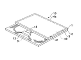
図1は、パッシブマトリクスタイプの液晶装置の外観を示す斜視図であり、図2は、その分解斜視図である。これらいずれの図面でも、液晶装置において画素を形成するためのストライプ電極については、その詳細な図示を省略してその一部のみを模式的に示してある。
【0012】
図1および図2において、液晶装置10は、たとえば透明なガラスによって形成された第1の透明基板1と、同じく透明なガラスによって形成された第2の透明基板2とを有している。これらの基板の一方にはシール剤3が印刷等によって形成され、このシール剤3を挟んで第1の透明基板1と第2の透明基板2とが接着固定されている。第1の透明基板1と第2の透明基板2との間隙(セルギャップ)のうち、シール剤3で区画形成された液晶封入領域40内には液晶41が封入されている。第1の透明基板1の外側表面には偏光板4aが粘着剤などによって貼られ、第2の透明基板2の外側表面にも偏光板(図示せず。)が粘着剤などで貼られている。
【0013】
第2の透明基板2は第1の透明基板1よりも大きいので、第2の透明基板2に第1の透明基板1を重ねた状態で、第2の透明基板2はその一部が第1の透明基板1の下端縁から張り出す。
【0014】
この張り出し部分にはIC実装領域9が形成されており、ここに半導体装置である駆動用IC13がフェイスダウンボンディングによりCOG実装される。この部分での実装構造は詳しくは後述するが、異方性導電膜を第2の透明基板2と駆動用IC13との間に挟んだ上で、それらを加熱圧着することによって行われる。従って、この部分では、異方性導電膜を介して第2の透明基板2のIC実装領域9の電極端子に駆動用IC13のバンプ電極が電気的接続している状態にある。
【0015】
また、第2の透明基板2において、IC実装領域9より下端側には入力端子12が形成されており、これらの入力端子12にはフレキシブルプリント配線基板(図示せず。)がヒートシールなどの方法で接続される。
【0016】
さらに、図1および図2では詳細な図示を省略してあるが、第1の透明基板1には、液晶封入領域40の内側で横方向に延びる複数のストライプ状電極、および液晶封入領域40の外側でストライプ状電極を各端子に配線接続するための配線パターンとからなる電極パターン(薄膜パターン)が形成されている。この電極パターンは、透明なITO膜(Indium Tin Oxide)などで形成されている。また、第2の透明基板2の内側表面にも、液晶封入領域40の内側で縦方向に延びる複数のストライプ状電極と、液晶封入領域40の外側でストライプ状電極をIC実装領域9になどに配線接続するための配線パターンとからなる電極パターン(薄膜パターン)が形成されている。この電極パターンも、透明なITO膜などで形成されている。
【0017】
このように構成した第1の透明基板1と第2の透明基板2とを所定箇所で電気的な接続を図りながら、図1に示すように貼り合わせてパネル(液晶パネル)を形成すると、第1の透明基板1のストライプ状電極と第2の透明基板2のストライプ状電極とは互いに交差し、各交差部分に画素が構成される。また、第1の透明基板1と第2の透明基板2との間隙において、液晶封入領域40には液晶41が封入される。従って、駆動用IC13に駆動用電力および駆動信号を送ると、駆動用IC13は、駆動信号に基づいて希望する適宜のストライプ状電極に電圧を印加して各画素における液晶41の配向状態を制御するので、液晶装置10に希望の像を表示する。
【0018】
(駆動用IC13の実装構造)
図3(A)、(B)はそれぞれ、駆動用IC13の第2の透明基板2との実装面を示す平面図、およびそのX−X′線断面図である。図4(A)〜(C)は、駆動用IC13を基板上に実装する方法を示す工程図である。
【0019】
図1および図2に示す液晶装置10において、IC実装領域9には多数の配線パターンの端部が集まっており、その配線パターンの先端部分が電極端子になっている。従って、液晶装置10において表示品位を向上しようとすると、画素数を増やすことになり、その結果、液晶パネルに構成されるストライプ状電極が増大し、その分、電極端子16(図4を参照。)が高密度に配置されることになる。
【0020】
従って、図3(A)に示すように、駆動用IC13では、第2の透明基板2との実装面13aに形成されているフェイスダウンボンディング用の複数のバンプ電極130も、液晶装置10において画素数を増やすほど、高密度に配置されることになる。すなわち、バンプ電極130は、チップの辺13bに沿って狭いピッチ、たとえば、40μm位のピッチで形成されることになる。バンプ電極130の表面形状は、概ね15μm角から20μm角の四角形であるので、隣接するバンプ電極130同士は、その表面131で概ね25μmから20μmといった狭い隙間を隔てているだけである。
【0021】
ここで、駆動用IC13のバンプ電極130は、図3(B)に示すように、第2の透明基板2の電極端子16に対向する表面131の側よりも根元部分132の方が細くなっている。このため、隣接するバンプ電極130同士は、その表面131で概ね25μmから20μmといった狭い隙間を隔てているが、根元部分132では表面131の側よりも広めの隙間を隔てている状態にある。
【0022】
このように構成した駆動用IC13の実装工程を説明しながら、本形態に係るIC実装構造を説明する。
【0023】
本形態に係る駆動用IC13を第2の透明基板2のIC実装領域9に実装する際には、まず、図4(A)に示すように、第2の透明基板2のIC実装領域9に異方性導電膜6を残した後、この異方性導電膜6の表面上に、バンプ電極130を下向きにして駆動用IC13を配置する。この異方性導電膜6では、プラスチック製のボールの表面に金属膜が形成された導電粒子60が熱硬化性の樹脂中に分散した状態にある。
【0024】
次に、図4(B)に示すように、圧着ヘッド5を用いて駆動用IC13を基板側に熱圧着する。その結果、異方性導電膜6の樹脂分が溶融する。
【0025】
従って、図4(C)に示すように、異方性導電膜6は溶融、流動、そして硬化反応後、異方性導電膜6の樹脂分が固化するので、駆動用IC13はIC実装領域9に実装されるとともに、駆動用IC13のバンプ電極130は、異方性導電膜6に含まれている導電粒子60を介して基板側の電極端子16に電気的接続する。
【0026】
このようにして駆動用IC13を実装した際に、異方性導電膜6は樹脂分が溶融して、図3(A)に矢印Aで示すように、樹脂分や導電粒子60が駆動用IC13と第2の透明基板2との間で、バンプ電極130の間を通って駆動用IC13の内側領域から外周側に流出しようとする。ここで、本形態では、駆動用IC13のバンプ電極130は、図3(B)および図4(A)〜(C)に示すように、根元部分132が細くなっているので、バンプ電極130を高密度に形成しても、隣接するバンプ電極130の間で根元部分132同士は広い隙間を隔てている。従って、異方性導電膜6の樹脂分や導電粒子60がバンプ電極130の間を通り抜けようとした際に、根元部分132の間の広い隙間を通り抜けていく。このため、バンプ電極130の間に多数の導電粒子60が溜まってしまうということがないので、導電粒子60はバンプ電極130同士を短絡させることがない。それ故、駆動用IC13のバンプ電極130を高密度に形成しても、高い信頼性を得ることができる。また、バンプ電極130は、第2の透明基板2の電極端子16に対向する表面131側が太くなっているので、第2の透明基板2の電極端子16とバンプ電極130とが対向する面積が広い。このため、バンプ電極130と電極端子16の間には、多数の導電粒子60が介在することになるので、バンプ電極130と電極端子16とは、良好に電気的接続する。
【0027】
(駆動用IC13のバンプ電極130の製造方法)
このような実装構造に用いる駆動用IC13の製造工程のうち、バンプ電極130を形成する方法を、図5を参照して説明する。図5(A)〜(E)は、バンプ電極130を形成する方法を示す工程断面図である。
【0028】
まず、図5(A)に示すように、駆動用IC13を構成する半導体基板135の表面に電極136を形成した後、図5(B)に示すように、感光性のレジスト150を塗布する。この感光性のレジスト150はネガタイプである。従って、露光マスク151を介して感光性のレジスト150を露光したとき、感光性のレジスト150のうち、露光マスク151の遮光部分152で覆われている領域のみが、図5(C)に示すように、エッチング工程(現像工程)で除去される。
【0029】
このようにして所定パターンのレジスト150を形成する際に、図5(B)に示す露光工程では、照射された光が感光性のレジスト150内で横方向にも拡散するので、露光部分155と非露光部分156の境界は逆テーパ形状となる。従って、図5(C)に示すように、レジスト150の開孔部分157は、側面壁が逆テーパ形状を有することになる。
【0030】
このようにして所定パターンのレジスト150を形成した後に、電極136の表面にめっきを施す。その結果、図5(D)に示すように、電極136の表面側では、レジスト150の開孔部分157を埋めるようにめっき135が施される。
【0031】
従って、めっきを終えた後、レジスト150を除去すると、図5(E)に示すように、表面131の側よりも根元部分132の方が細いバンプ電極130を形成することができる。
【0032】
(電子機器への搭載例)
図7は、本発明に係る電子機器の一実施形態である携帯電話機を示している。ここに示す携帯電話機30は、アンテナ31、スピーカ32、液晶装置10、キースイッチ33、マイクロホン34等といった各種構成要素を、筐体としての外装ケース36に格納することによって構成される。また、外装ケース36の内部には、上記の各構成要素の動作を制御するための制御回路を搭載した制御回路基板37が設けられる。液晶装置10は図1に示した液晶装置10によって構成される。
【0033】
この携帯電話機30では、キースイッチ33及びマイクロホン34を通して入力される信号や、アンテナ31によって受信した受信データ等が制御回路基板37上の制御回路へ入力される。そしてその制御回路は、入力した各種データに基づいて液晶装置10の表示面内に数字、文字、絵柄等といった像を表示し、さらに、アンテナ31から送信データを送信する。また、図7の実施形態では、電子機器としての携帯電話機に本発明の液晶装置を用いる場合を例示したが、本発明の液晶装置はそれ以外の電子機器、例えば携帯情報端末、電子手帳、ビデオカメラのファインダー等に適用することもできる。
【0034】
また図6(a)、(b)は、本形態の液晶装置10を搭載した携帯電話(電子機器)の要部を示す断面図である。
【0035】
本形態の液晶装置10を搭載した電子機器の一例として、図6に示す携帯電話100では、液晶装置10の第1の透明基板1の側には、アクリル樹脂製あるいはポリカーボネート製の透明な導光板19が重ねて配置され、この導光板19と第2の透明基板2との間からフレキシブル配線基板120が引き出され、携帯電話100本体の回路基板であるプリント配線基板90に電気的及び機械的に接続されている。導光板19の側方(又は端部)に隣接して、導光板19の端部(光入射部)に向かって光を出射するバックライト用発光素子50が配置される。このようなバックライト用発光素子50としてはLEDなどが用いられ、プリント配線基板90上に実装されている。本実施例ではバックライト用発光素子50がプリント配線基板90上に実装されているが、導光板19への入射が可能な位置であればフレキシブル配線基板120上に実装されていても良く、またプリント配線基板90とは別のサブ基板に実装されていてもよい。ここで、液晶装置10は導光板19に両面テープ等により固定されるとともにフレーム110で抑えられている。また、導光板19は液晶装置10を固定するとともにプリント配線基板90と嵌合等の方法により一体的に保持し、同時に携帯電話100のフレーム110にも固定されている。また、第2の透明基板2の側にはカバーガラス111が被せられる。
【0036】
(その他の実施の形態)
なお、上記の形態では、液晶パネルを構成する第2の透明基板2に対して駆動用IC13をCOG実装する例であったが、駆動用IC13は、液晶パネルに対して回路接続するフレキシブル配線基板に対してCOF実装される場合もある。このような場合でも、図4(A)〜(C)を参照して説明した実装工程において、第2の透明基板2に代えて、フレキシブル配線基板上に駆動用IC13を異方性導電膜6を介して実装すればよい。
【0037】
【発明の効果】
以上説明したように、本発明では、ICのバンプ電極は根元部分が細くなっているので、バンプ電極を高密度に形成しても、隣接するバンプ電極の間で根元部分同士が広い隙間を隔てている。従って、ICを異方性導電膜を介して基板に実装する際に異方性導電膜が溶融してバンプ電極の間から流出しようとするときに、隣接し合うバンプ電極の根元同士の間に多数の導電粒子が溜まることがないので、導電粒子はバンプ電極同士を短絡させることがない。それ故、ICのバンプ電極を高密度に形成しても、高い信頼性を得ることができる。また、バンプ電極は、基板の電極端子に対向する表面側が太くなっているので、基板の電極端子とバンプ電極とが対向する面積が広い。よって、バンプ電極と電極端子の間には、多数の導電粒子が介在することになるので、バンプ電極と電極端子とは、良好に電気的接続する。
【図面の簡単な説明】
【図1】図1は、本発明を適用した液晶装置の外観を示す斜視図である。
【図2】図1に示す液晶装置の分解斜視図である。
【図3】(A)、(B)はそれぞれ、図1に示す駆動用ICに形成したバンプ電極の配置を示す平面図、およびそのX−X′断面図である。
【図4】(A)〜(C)は、図3に示す駆動用ICを液晶パネルを構成する第2の透明基板上に実装する工程を示す工程断面図である。
【図5】(A)〜(E)は、図3に示す駆動用ICのバンプ電極を形成する方法を示す工程断面図である。
【図6】(A)、(B)はそれぞれ、本発明を適用した液晶装置を搭載した携帯電話(電子機器)の要部を示す断面図である。
【図7】本発明を適用した液晶装置を搭載した携帯電話(電子機器)を示す説明図である。
【図8】(A)〜(C)は、基板に対する従来の駆動用ICの実装工程を示す工程断面図である。
【符号の説明】
1 第1の透明基板
2 第2の透明基板
3 シール剤
6 異方性導電膜
9 IC実装領域
10 液晶装置
13 駆動用IC
16 電極端子
19 導光板
40 液晶封入領域
41 液晶
50 バックライト用発光素子
60 異方性導電膜の導電粒子
90 プリント配線基板
100 携帯電話(電子機器)
110 フレーム
111 カバーガラス
120 フレキシブル配線基板
130 バンプ電極
131 バンプ電極の表面
132 バンプ電極の根元部分
Claims (3)
- 半導体基板に電極を形成する工程と、
前記半導体基板上にネガタイプの感光性樹脂を塗布する工程と、
マスクを用いて前記感光性樹脂を、前記感光性樹脂内で横方向に拡散する条件で露光する工程と、
露光された前記感光性樹脂を現像する工程と、
現像によって開孔された部分にめっきを施して複数のバンプ電極を形成する工程と、
前記感光性樹脂を除去する工程と、
少なくとも電極端子上に導電粒子を含有する異方性導電膜が形成されている基板と、前記半導体装置とを圧着して、前記電極端子と前記バンプ電極とを前記異方性導電膜を介して電気的に接続する工程と、を有し、
前記複数のバンプ電極は、前記複数のバンプ電極のうち、隣り合う第1のバンプ電極と第2のバンプ電極とが短絡しないように、前記第1のバンプ電極の表面側と前記第2のバンプ電極の表面側との距離が、前記第1のバンプ電極の根元側と前記第2のバンプ電極の根元側との距離よりも小さく形成されることを特徴とする半導体装置の実装構造の製造方法。 - 第1の基板と第2の基板との間に液晶が封入された液晶パネルを有する液晶装置であって、少なくとも前記第1の基板または前記第2の基板は請求項1に規定する半導体装置の実装構造の製造方法により製造された実装構造を有していることを特徴とする液晶装置。
- 請求項2に規定する液晶装置を搭載したことを特徴とする電子機器。
Priority Applications (5)
| Application Number | Priority Date | Filing Date | Title |
|---|---|---|---|
| JP06045999A JP3826605B2 (ja) | 1999-03-08 | 1999-03-08 | 半導体装置の実装構造の製造方法、液晶装置、および電子機器 |
| TW089103081A TW444300B (en) | 1999-03-08 | 2000-02-22 | Semiconductor device, structure for mounting the semiconductor device, liquid crystal device, and electronic equipment |
| KR10-2000-0010619A KR100516597B1 (ko) | 1999-03-08 | 2000-03-03 | 반도체 장치, 반도체 장치의 실장 구조, 액정 장치 및 전자 기기 |
| US09/519,436 US6448663B1 (en) | 1999-03-08 | 2000-03-03 | Semiconductor device, semiconductor device mounting structure, liquid crystal device, and electronic apparatus |
| CNB001041207A CN1181542C (zh) | 1999-03-08 | 2000-03-07 | 半导体装置、半导体装置的安装结构、液晶装置和电子装置 |
Applications Claiming Priority (1)
| Application Number | Priority Date | Filing Date | Title |
|---|---|---|---|
| JP06045999A JP3826605B2 (ja) | 1999-03-08 | 1999-03-08 | 半導体装置の実装構造の製造方法、液晶装置、および電子機器 |
Publications (3)
| Publication Number | Publication Date |
|---|---|
| JP2000260798A JP2000260798A (ja) | 2000-09-22 |
| JP2000260798A5 JP2000260798A5 (ja) | 2005-02-24 |
| JP3826605B2 true JP3826605B2 (ja) | 2006-09-27 |
Family
ID=13142881
Family Applications (1)
| Application Number | Title | Priority Date | Filing Date |
|---|---|---|---|
| JP06045999A Expired - Lifetime JP3826605B2 (ja) | 1999-03-08 | 1999-03-08 | 半導体装置の実装構造の製造方法、液晶装置、および電子機器 |
Country Status (5)
| Country | Link |
|---|---|
| US (1) | US6448663B1 (ja) |
| JP (1) | JP3826605B2 (ja) |
| KR (1) | KR100516597B1 (ja) |
| CN (1) | CN1181542C (ja) |
| TW (1) | TW444300B (ja) |
Families Citing this family (44)
| Publication number | Priority date | Publication date | Assignee | Title |
|---|---|---|---|---|
| TWI240241B (en) * | 2000-05-04 | 2005-09-21 | Koninkl Philips Electronics Nv | Assembly of a display device and an illumination system |
| US6642613B1 (en) * | 2000-05-09 | 2003-11-04 | National Semiconductor Corporation | Techniques for joining an opto-electronic module to a semiconductor package |
| US6995753B2 (en) * | 2000-06-06 | 2006-02-07 | Semiconductor Energy Laboratory Co., Ltd. | Display device and method of manufacturing the same |
| JP3892650B2 (ja) * | 2000-07-25 | 2007-03-14 | 株式会社日立製作所 | 液晶表示装置 |
| JP3781967B2 (ja) * | 2000-12-25 | 2006-06-07 | 株式会社日立製作所 | 表示装置 |
| JP3756418B2 (ja) * | 2001-02-28 | 2006-03-15 | 株式会社日立製作所 | 液晶表示装置及びその製造方法 |
| US6806938B2 (en) * | 2001-08-30 | 2004-10-19 | Kyocera Corporation | Liquid crystal display device with particular on substrate wiring, portable terminal and display equipment provided with the liquid crystal display device |
| JP2003121815A (ja) * | 2001-10-16 | 2003-04-23 | Nec Access Technica Ltd | Lcdの保持構造 |
| JP3573150B2 (ja) | 2002-01-25 | 2004-10-06 | セイコーエプソン株式会社 | 半導体装置及びこれを含む電気光学装置 |
| KR100499134B1 (ko) * | 2002-10-28 | 2005-07-04 | 삼성전자주식회사 | 압축 접합 방법 |
| JP2004184805A (ja) * | 2002-12-05 | 2004-07-02 | Tohoku Pioneer Corp | 導電配線の接続構造 |
| KR20040075377A (ko) * | 2003-02-20 | 2004-08-30 | 삼성전자주식회사 | 구동 아이씨 및 이를 갖는 디스플레이 장치 |
| CN1325983C (zh) * | 2003-05-27 | 2007-07-11 | 友达光电股份有限公司 | 液晶显示面板的封装结构及其制作工艺 |
| JP4004994B2 (ja) | 2003-06-05 | 2007-11-07 | 株式会社アドバンスト・ディスプレイ | 表示装置 |
| CN100356559C (zh) * | 2003-09-24 | 2007-12-19 | 财团法人工业技术研究院 | 倒装芯片封装结构及其制造方法 |
| TWI277815B (en) * | 2004-01-16 | 2007-04-01 | Hannstar Display Corp | Liquid crystal display and manufacturing method of liquid crystal display including substrate |
| CN100416343C (zh) * | 2004-01-21 | 2008-09-03 | 友达光电股份有限公司 | 增加金属连线可靠度的结构 |
| CN1297840C (zh) * | 2004-03-25 | 2007-01-31 | 友达光电股份有限公司 | 显示器的导线结构 |
| US7767516B2 (en) * | 2005-05-31 | 2010-08-03 | Semiconductor Energy Laboratory Co., Ltd | Semiconductor device, manufacturing method thereof, and manufacturing method of antenna |
| JP4851255B2 (ja) * | 2006-07-14 | 2012-01-11 | 株式会社 日立ディスプレイズ | 表示装置 |
| JP4920330B2 (ja) * | 2006-07-18 | 2012-04-18 | ソニー株式会社 | 実装構造体の実装方法、発光ダイオードディスプレイの実装方法、発光ダイオードバックライトの実装方法および電子機器の実装方法 |
| JP2008235556A (ja) * | 2007-03-20 | 2008-10-02 | Sumitomo Electric Ind Ltd | 配線板モジュール及び該配線板モジュールの製造方法 |
| KR101285273B1 (ko) * | 2007-06-15 | 2013-07-23 | 엘지디스플레이 주식회사 | 이동통신기기 |
| CN101216619B (zh) * | 2008-01-10 | 2010-09-22 | 友达光电股份有限公司 | 平面显示器及其制造方法和光电装置及其制造方法 |
| CN101556838B (zh) * | 2008-04-09 | 2011-06-01 | 北京京东方光电科技有限公司 | 各向异性导电膜 |
| TW201123377A (en) * | 2009-12-16 | 2011-07-01 | Raydium Semiconductor Corp | Electronic chip and substrate with void |
| US9142533B2 (en) * | 2010-05-20 | 2015-09-22 | Taiwan Semiconductor Manufacturing Company, Ltd. | Substrate interconnections having different sizes |
| KR101375298B1 (ko) * | 2011-12-20 | 2014-03-19 | 제일모직주식회사 | 전도성 미립자 및 이를 포함하는 이방 전도성 필름 |
| US9425136B2 (en) | 2012-04-17 | 2016-08-23 | Taiwan Semiconductor Manufacturing Company, Ltd. | Conical-shaped or tier-shaped pillar connections |
| US9646923B2 (en) | 2012-04-17 | 2017-05-09 | Taiwan Semiconductor Manufacturing Company, Ltd. | Semiconductor devices, methods of manufacture thereof, and packaged semiconductor devices |
| US9299674B2 (en) | 2012-04-18 | 2016-03-29 | Taiwan Semiconductor Manufacturing Company, Ltd. | Bump-on-trace interconnect |
| US9111817B2 (en) | 2012-09-18 | 2015-08-18 | Taiwan Semiconductor Manufacturing Company, Ltd. | Bump structure and method of forming same |
| US8950011B2 (en) | 2013-05-22 | 2015-02-03 | International Business Machines Corporation | Targeted sequencing of biomolecules by pulling through a liquid-liquid interface with an atomic force microscope |
| JP6645730B2 (ja) * | 2014-01-28 | 2020-02-14 | デクセリアルズ株式会社 | 接続体及び接続体の製造方法 |
| KR20150094125A (ko) * | 2014-02-10 | 2015-08-19 | 한국전자통신연구원 | 반도체 소자 및 이를 제조하는 방법 |
| JP6476747B2 (ja) * | 2014-10-28 | 2019-03-06 | デクセリアルズ株式会社 | 異方性導電フィルム及び接続構造体 |
| US10170403B2 (en) * | 2014-12-17 | 2019-01-01 | Kinsus Interconnect Technology Corp. | Ameliorated compound carrier board structure of flip-chip chip-scale package |
| WO2016190197A1 (ja) * | 2015-05-22 | 2016-12-01 | シャープ株式会社 | 半導体装置 |
| CN106486511B (zh) * | 2015-08-25 | 2020-04-28 | 上海和辉光电有限公司 | 一种显示器件及制备有机发光二极管显示面板的方法 |
| TWI696300B (zh) * | 2016-03-15 | 2020-06-11 | 晶元光電股份有限公司 | 半導體裝置及其製造方法 |
| JP6769721B2 (ja) * | 2016-03-25 | 2020-10-14 | デクセリアルズ株式会社 | 電子部品、異方性接続構造体、電子部品の設計方法 |
| KR20180065162A (ko) * | 2016-12-07 | 2018-06-18 | 서울바이오시스 주식회사 | 디스플레이 장치 및 그의 전극 연결 방법 |
| CN109037998B (zh) * | 2018-08-08 | 2020-06-05 | 武汉华星光电半导体显示技术有限公司 | 电连接组件及显示装置、电连接方法 |
| US11139262B2 (en) * | 2019-02-07 | 2021-10-05 | Micron Technology, Inc. | Use of pre-channeled materials for anisotropic conductors |
Family Cites Families (5)
| Publication number | Priority date | Publication date | Assignee | Title |
|---|---|---|---|---|
| US5226232A (en) * | 1990-05-18 | 1993-07-13 | Hewlett-Packard Company | Method for forming a conductive pattern on an integrated circuit |
| JP3152796B2 (ja) * | 1993-05-28 | 2001-04-03 | 株式会社東芝 | 半導体装置およびその製造方法 |
| JP3225800B2 (ja) * | 1995-08-09 | 2001-11-05 | 三菱電機株式会社 | 半導体装置 |
| KR100232678B1 (ko) * | 1996-12-18 | 1999-12-01 | 구본준 | 돌기가 형성된 범프 및 그 제조방법 |
| US5903056A (en) * | 1997-04-21 | 1999-05-11 | Lucent Technologies Inc. | Conductive polymer film bonding technique |
-
1999
- 1999-03-08 JP JP06045999A patent/JP3826605B2/ja not_active Expired - Lifetime
-
2000
- 2000-02-22 TW TW089103081A patent/TW444300B/zh not_active IP Right Cessation
- 2000-03-03 US US09/519,436 patent/US6448663B1/en not_active Expired - Lifetime
- 2000-03-03 KR KR10-2000-0010619A patent/KR100516597B1/ko active IP Right Grant
- 2000-03-07 CN CNB001041207A patent/CN1181542C/zh not_active Expired - Lifetime
Also Published As
| Publication number | Publication date |
|---|---|
| JP2000260798A (ja) | 2000-09-22 |
| KR100516597B1 (ko) | 2005-09-22 |
| CN1266283A (zh) | 2000-09-13 |
| TW444300B (en) | 2001-07-01 |
| US20020100974A1 (en) | 2002-08-01 |
| CN1181542C (zh) | 2004-12-22 |
| KR20000071406A (ko) | 2000-11-25 |
| US6448663B1 (en) | 2002-09-10 |
Similar Documents
| Publication | Publication Date | Title |
|---|---|---|
| JP3826605B2 (ja) | 半導体装置の実装構造の製造方法、液晶装置、および電子機器 | |
| JP3139549B2 (ja) | アクティブマトリクス型液晶表示装置 | |
| US6542374B1 (en) | Circuit board, method for manufacturing the circuit board, and display device and electronic equipment employing the circuit board | |
| JP2000260798A5 (ja) | ||
| JP2007041389A (ja) | 表示装置及びその製造方法 | |
| KR20090058987A (ko) | 액정표시장치의 제조방법 및 액정표시장치의 필름 캐리어테이프 제조방법 | |
| KR20080046371A (ko) | 액정표시장치 구동회로 및 그의 제조방법과 액정표시장치구동회로가 실장 된 액정표시장치 | |
| US20070076577A1 (en) | Mount Structure, Electro-Optical Device, Method of Manufacturing Electro-Optical Device, and Electronic Apparatus | |
| JP3933094B2 (ja) | 電子部品の実装方法 | |
| JP2006113436A (ja) | 表示装置 | |
| TWI292073B (ja) | ||
| US6741315B1 (en) | Liquid crystal device and electronic apparatus | |
| JP4103835B2 (ja) | 電子部品の製造方法 | |
| JPH11354564A (ja) | Icチップ、ic構造体、液晶装置及び電子機器 | |
| JP2001230001A (ja) | 接続構造、電気光学装置および電子機器 | |
| JP3695265B2 (ja) | 表示装置及び電子機器 | |
| JP2000284261A (ja) | 液晶装置及び電子機器 | |
| JPS60225120A (ja) | 液晶表示装置 | |
| JP3675185B2 (ja) | 配線基板、液晶装置及び電子機器 | |
| JP4267870B2 (ja) | 表示装置の製造方法 | |
| JP2001318619A (ja) | 電気光学装置、電気光学装置の製造方法および電子機器 | |
| CN114173467A (zh) | 印刷电路基板、显示装置以及显示装置的制造方法 | |
| JP3760624B2 (ja) | 液晶表示装置およびそれを利用した電子機器 | |
| JP2000275672A (ja) | 液晶装置、液晶装置の製造方法及び電子機器 | |
| JP2594874Y2 (ja) | 液晶表示装置 |
Legal Events
| Date | Code | Title | Description |
|---|---|---|---|
| A521 | Written amendment |
Free format text: JAPANESE INTERMEDIATE CODE: A523 Effective date: 20040318 |
|
| A621 | Written request for application examination |
Free format text: JAPANESE INTERMEDIATE CODE: A621 Effective date: 20040318 |
|
| A977 | Report on retrieval |
Free format text: JAPANESE INTERMEDIATE CODE: A971007 Effective date: 20041018 |
|
| A131 | Notification of reasons for refusal |
Free format text: JAPANESE INTERMEDIATE CODE: A131 Effective date: 20060314 |
|
| A521 | Written amendment |
Free format text: JAPANESE INTERMEDIATE CODE: A523 Effective date: 20060512 |
|
| TRDD | Decision of grant or rejection written | ||
| A01 | Written decision to grant a patent or to grant a registration (utility model) |
Free format text: JAPANESE INTERMEDIATE CODE: A01 Effective date: 20060613 |
|
| A61 | First payment of annual fees (during grant procedure) |
Free format text: JAPANESE INTERMEDIATE CODE: A61 Effective date: 20060626 |
|
| R150 | Certificate of patent or registration of utility model |
Free format text: JAPANESE INTERMEDIATE CODE: R150 |
|
| FPAY | Renewal fee payment (event date is renewal date of database) |
Free format text: PAYMENT UNTIL: 20100714 Year of fee payment: 4 |
|
| FPAY | Renewal fee payment (event date is renewal date of database) |
Free format text: PAYMENT UNTIL: 20110714 Year of fee payment: 5 |
|
| FPAY | Renewal fee payment (event date is renewal date of database) |
Free format text: PAYMENT UNTIL: 20110714 Year of fee payment: 5 |
|
| FPAY | Renewal fee payment (event date is renewal date of database) |
Free format text: PAYMENT UNTIL: 20120714 Year of fee payment: 6 |
|
| FPAY | Renewal fee payment (event date is renewal date of database) |
Free format text: PAYMENT UNTIL: 20120714 Year of fee payment: 6 |
|
| FPAY | Renewal fee payment (event date is renewal date of database) |
Free format text: PAYMENT UNTIL: 20130714 Year of fee payment: 7 |
|
| R250 | Receipt of annual fees |
Free format text: JAPANESE INTERMEDIATE CODE: R250 |
|
| S111 | Request for change of ownership or part of ownership |
Free format text: JAPANESE INTERMEDIATE CODE: R313113 |
|
| S111 | Request for change of ownership or part of ownership |
Free format text: JAPANESE INTERMEDIATE CODE: R313113 |
|
| R371 | Transfer withdrawn |
Free format text: JAPANESE INTERMEDIATE CODE: R371 |
|
| S111 | Request for change of ownership or part of ownership |
Free format text: JAPANESE INTERMEDIATE CODE: R313113 |
|
| R350 | Written notification of registration of transfer |
Free format text: JAPANESE INTERMEDIATE CODE: R350 |
|
| R250 | Receipt of annual fees |
Free format text: JAPANESE INTERMEDIATE CODE: R250 |
|
| R250 | Receipt of annual fees |
Free format text: JAPANESE INTERMEDIATE CODE: R250 |
|
| R250 | Receipt of annual fees |
Free format text: JAPANESE INTERMEDIATE CODE: R250 |
|
| EXPY | Cancellation because of completion of term |