JP2022166301A - 積層電子部品 - Google Patents
積層電子部品 Download PDFInfo
- Publication number
- JP2022166301A JP2022166301A JP2022133821A JP2022133821A JP2022166301A JP 2022166301 A JP2022166301 A JP 2022166301A JP 2022133821 A JP2022133821 A JP 2022133821A JP 2022133821 A JP2022133821 A JP 2022133821A JP 2022166301 A JP2022166301 A JP 2022166301A
- Authority
- JP
- Japan
- Prior art keywords
- electronic component
- external electrodes
- multilayer electronic
- sintered body
- external electrode
- Prior art date
- Legal status (The legal status is an assumption and is not a legal conclusion. Google has not performed a legal analysis and makes no representation as to the accuracy of the status listed.)
- Granted
Links
Images


Classifications
-
- H—ELECTRICITY
- H01—ELECTRIC ELEMENTS
- H01C—RESISTORS
- H01C17/00—Apparatus or processes specially adapted for manufacturing resistors
- H01C17/30—Apparatus or processes specially adapted for manufacturing resistors adapted for baking
-
- H—ELECTRICITY
- H01—ELECTRIC ELEMENTS
- H01C—RESISTORS
- H01C1/00—Details
- H01C1/14—Terminals or tapping points specially adapted for resistors; Arrangements of terminals or tapping points on resistors
- H01C1/148—Terminals or tapping points specially adapted for resistors; Arrangements of terminals or tapping points on resistors the terminals embracing or surrounding the resistive element
-
- H—ELECTRICITY
- H01—ELECTRIC ELEMENTS
- H01C—RESISTORS
- H01C17/00—Apparatus or processes specially adapted for manufacturing resistors
- H01C17/28—Apparatus or processes specially adapted for manufacturing resistors adapted for applying terminals
-
- H—ELECTRICITY
- H01—ELECTRIC ELEMENTS
- H01C—RESISTORS
- H01C17/00—Apparatus or processes specially adapted for manufacturing resistors
- H01C17/28—Apparatus or processes specially adapted for manufacturing resistors adapted for applying terminals
- H01C17/281—Apparatus or processes specially adapted for manufacturing resistors adapted for applying terminals by thick film techniques
- H01C17/283—Precursor compositions therefor, e.g. pastes, inks, glass frits
- H01C17/285—Precursor compositions therefor, e.g. pastes, inks, glass frits applied to zinc or cadmium oxide resistors
-
- H—ELECTRICITY
- H01—ELECTRIC ELEMENTS
- H01C—RESISTORS
- H01C7/00—Non-adjustable resistors formed as one or more layers or coatings; Non-adjustable resistors made from powdered conducting material or powdered semi-conducting material with or without insulating material
- H01C7/10—Non-adjustable resistors formed as one or more layers or coatings; Non-adjustable resistors made from powdered conducting material or powdered semi-conducting material with or without insulating material voltage responsive, i.e. varistors
- H01C7/1006—Thick film varistors
-
- H—ELECTRICITY
- H01—ELECTRIC ELEMENTS
- H01C—RESISTORS
- H01C7/00—Non-adjustable resistors formed as one or more layers or coatings; Non-adjustable resistors made from powdered conducting material or powdered semi-conducting material with or without insulating material
- H01C7/18—Non-adjustable resistors formed as one or more layers or coatings; Non-adjustable resistors made from powdered conducting material or powdered semi-conducting material with or without insulating material comprising a plurality of layers stacked between terminals
-
- H—ELECTRICITY
- H01—ELECTRIC ELEMENTS
- H01C—RESISTORS
- H01C17/00—Apparatus or processes specially adapted for manufacturing resistors
- H01C17/28—Apparatus or processes specially adapted for manufacturing resistors adapted for applying terminals
- H01C17/281—Apparatus or processes specially adapted for manufacturing resistors adapted for applying terminals by thick film techniques
-
- Y—GENERAL TAGGING OF NEW TECHNOLOGICAL DEVELOPMENTS; GENERAL TAGGING OF CROSS-SECTIONAL TECHNOLOGIES SPANNING OVER SEVERAL SECTIONS OF THE IPC; TECHNICAL SUBJECTS COVERED BY FORMER USPC CROSS-REFERENCE ART COLLECTIONS [XRACs] AND DIGESTS
- Y10—TECHNICAL SUBJECTS COVERED BY FORMER USPC
- Y10T—TECHNICAL SUBJECTS COVERED BY FORMER US CLASSIFICATION
- Y10T29/00—Metal working
- Y10T29/43—Electric condenser making
Landscapes
- Engineering & Computer Science (AREA)
- Microelectronics & Electronic Packaging (AREA)
- Physics & Mathematics (AREA)
- Electromagnetism (AREA)
- Manufacturing & Machinery (AREA)
- Ceramic Capacitors (AREA)
- Fixed Capacitors And Capacitor Manufacturing Machines (AREA)
- Thermistors And Varistors (AREA)
- Details Of Resistors (AREA)
- Apparatuses And Processes For Manufacturing Resistors (AREA)
Abstract
【解決手段】その内部に内部電極を有する焼結体と、焼結体の側面に設けられ、内部電極に接続された外部電極と、を含む個体部品と、外部電極に、接合層を介して接続されたリード端子と、を備えた積層電子部品であって、個体部品は、積層電子部品が実装物に実装されている状態で実装物に対向する実装面を有し、接合層は、外部電極からリード端子に沿って前記実装面を超えて広がっている。
【選択図】図1B
Description
化することができる。
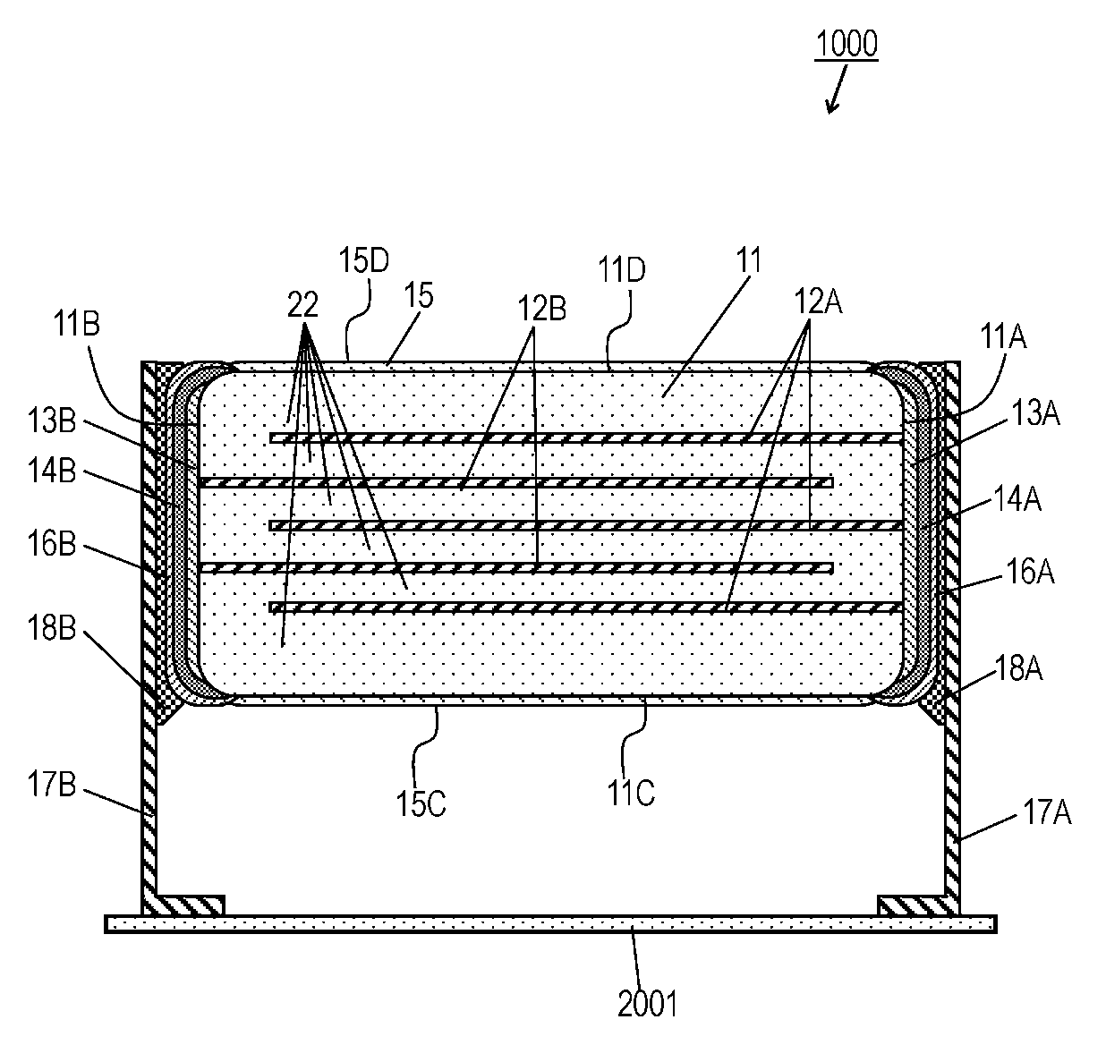
、17Bに沿って焼結体11の側面11A、11Bから実装面11Cを超えて実装物2001に向かって濡れ広げることができる。このように構成することにより、リード端子17A、17B側からの応力を分散することができ、積層電子部品1000の信頼性をさらに向上させることができる。
12A,12B 内部電極
13A,13B 外部電極(第1の外部電極)
14A,14B 外部電極(第2の外部電極)
15 絶縁層
16A,16B めっき層
17A,17B リード端子
18A,18B 接合層
Claims (3)
- その内部に内部電極を有する焼結体と、
前記焼結体の側面に設けられ、前記内部電極に接続された外部電極と、
を含む個体部品と、
前記外部電極に、接合層を介して接続されたリード端子と、
を備えた積層電子部品であって、
前記個体部品は、前記積層電子部品が実装物に実装されている状態で前記実装物に対向する実装面を有し、
前記接合層は、前記外部電極から前記リード端子に沿って前記実装面を超えて広がっている、積層電子部品。 - 前記接合層は、はんだを含む、請求項1に記載の積層電子部品。
- 前記リード端子は、L字状に屈曲されている、請求項1または2に記載の積層電子部品。
Applications Claiming Priority (4)
| Application Number | Priority Date | Filing Date | Title |
|---|---|---|---|
| JP2017197380 | 2017-10-11 | ||
| JP2017197380 | 2017-10-11 | ||
| JP2019547963A JP7361250B2 (ja) | 2017-10-11 | 2018-09-19 | 積層電子部品の製造方法 |
| PCT/JP2018/034534 WO2019073762A1 (ja) | 2017-10-11 | 2018-09-19 | 積層電子部品の製造方法 |
Related Parent Applications (1)
| Application Number | Title | Priority Date | Filing Date |
|---|---|---|---|
| JP2019547963A Division JP7361250B2 (ja) | 2017-10-11 | 2018-09-19 | 積層電子部品の製造方法 |
Publications (2)
| Publication Number | Publication Date |
|---|---|
| JP2022166301A true JP2022166301A (ja) | 2022-11-01 |
| JP7394292B2 JP7394292B2 (ja) | 2023-12-08 |
Family
ID=66100032
Family Applications (2)
| Application Number | Title | Priority Date | Filing Date |
|---|---|---|---|
| JP2019547963A Active JP7361250B2 (ja) | 2017-10-11 | 2018-09-19 | 積層電子部品の製造方法 |
| JP2022133821A Active JP7394292B2 (ja) | 2017-10-11 | 2022-08-25 | 積層電子部品 |
Family Applications Before (1)
| Application Number | Title | Priority Date | Filing Date |
|---|---|---|---|
| JP2019547963A Active JP7361250B2 (ja) | 2017-10-11 | 2018-09-19 | 積層電子部品の製造方法 |
Country Status (4)
| Country | Link |
|---|---|
| US (2) | US11387023B2 (ja) |
| JP (2) | JP7361250B2 (ja) |
| CN (1) | CN110945605B (ja) |
| WO (1) | WO2019073762A1 (ja) |
Families Citing this family (3)
| Publication number | Priority date | Publication date | Assignee | Title |
|---|---|---|---|---|
| JP2022170166A (ja) * | 2021-04-28 | 2022-11-10 | Tdk株式会社 | 電子部品 |
| JP7802462B2 (ja) * | 2021-04-28 | 2026-01-20 | Tdk株式会社 | 電子部品 |
| KR20230103096A (ko) | 2021-12-31 | 2023-07-07 | 삼성전기주식회사 | 적층형 전자 부품 |
Citations (8)
| Publication number | Priority date | Publication date | Assignee | Title |
|---|---|---|---|---|
| JPS58111915U (ja) * | 1982-01-25 | 1983-07-30 | 日本電気株式会社 | 積層セラミツクコンデンサ |
| JPS6284921U (ja) * | 1985-11-15 | 1987-05-30 | ||
| JP2000306764A (ja) * | 1999-04-23 | 2000-11-02 | Murata Mfg Co Ltd | セラミック電子部品及びその製造方法 |
| JP2003068563A (ja) * | 2001-08-22 | 2003-03-07 | Tdk Corp | ラジアルリード型積層セラミック電子部品 |
| JP2008294180A (ja) * | 2007-05-24 | 2008-12-04 | Murata Mfg Co Ltd | リード線付き電子部品、及び該リード線付き電子部品の製造方法 |
| JP2010161172A (ja) * | 2009-01-07 | 2010-07-22 | Tdk Corp | 積層コンデンサ及び積層コンデンサの実装構造 |
| JP2016189382A (ja) * | 2015-03-30 | 2016-11-04 | 日本ケミコン株式会社 | コンデンサおよびその製造方法 |
| JP2019012749A (ja) * | 2017-06-29 | 2019-01-24 | 太陽誘電株式会社 | セラミック電子部品及びその製造方法、並びに電子部品実装基板 |
Family Cites Families (13)
| Publication number | Priority date | Publication date | Assignee | Title |
|---|---|---|---|---|
| JPH06295803A (ja) * | 1993-04-07 | 1994-10-21 | Mitsubishi Materials Corp | チップ型サーミスタ及びその製造方法 |
| JP3640273B2 (ja) * | 1995-03-24 | 2005-04-20 | Tdk株式会社 | 積層型バリスタ |
| DE69632659T2 (de) * | 1995-03-24 | 2005-06-09 | Tdk Corp. | Vielschichtvaristor |
| JP2000164406A (ja) * | 1998-11-25 | 2000-06-16 | Murata Mfg Co Ltd | チップ型電子部品とその製造方法 |
| JP2000223359A (ja) | 1999-01-29 | 2000-08-11 | Murata Mfg Co Ltd | セラミック電子部品 |
| JP2000235932A (ja) | 1999-02-16 | 2000-08-29 | Murata Mfg Co Ltd | セラミック電子部品 |
| US20080239621A1 (en) * | 2007-03-29 | 2008-10-02 | Azizuddin Tajuddin | Clip-on leadframe |
| JP5664574B2 (ja) | 2011-03-18 | 2015-02-04 | 株式会社村田製作所 | 積層セラミックコンデンサ |
| JP5375877B2 (ja) * | 2011-05-25 | 2013-12-25 | Tdk株式会社 | 積層コンデンサ及び積層コンデンサの製造方法 |
| CN203085375U (zh) * | 2012-12-24 | 2013-07-24 | 日科能高电子(苏州)有限公司 | 铝电解电容器引脚切断机 |
| JP2015012052A (ja) | 2013-06-27 | 2015-01-19 | 株式会社村田製作所 | セラミックサーミスタ |
| CN205752078U (zh) * | 2016-05-10 | 2016-11-30 | 南京萨特科技发展有限公司 | 引脚结构大电流微型熔断器 |
| CN106024231B (zh) * | 2016-05-27 | 2018-07-10 | 辰硕电子(九江)有限公司 | 一种氧化锌压敏电阻器瓷片的制备方法 |
-
2018
- 2018-09-19 WO PCT/JP2018/034534 patent/WO2019073762A1/ja not_active Ceased
- 2018-09-19 JP JP2019547963A patent/JP7361250B2/ja active Active
- 2018-09-19 CN CN201880048740.9A patent/CN110945605B/zh active Active
- 2018-09-19 US US16/622,572 patent/US11387023B2/en active Active
-
2022
- 2022-06-13 US US17/838,961 patent/US20220310291A1/en not_active Abandoned
- 2022-08-25 JP JP2022133821A patent/JP7394292B2/ja active Active
Patent Citations (8)
| Publication number | Priority date | Publication date | Assignee | Title |
|---|---|---|---|---|
| JPS58111915U (ja) * | 1982-01-25 | 1983-07-30 | 日本電気株式会社 | 積層セラミツクコンデンサ |
| JPS6284921U (ja) * | 1985-11-15 | 1987-05-30 | ||
| JP2000306764A (ja) * | 1999-04-23 | 2000-11-02 | Murata Mfg Co Ltd | セラミック電子部品及びその製造方法 |
| JP2003068563A (ja) * | 2001-08-22 | 2003-03-07 | Tdk Corp | ラジアルリード型積層セラミック電子部品 |
| JP2008294180A (ja) * | 2007-05-24 | 2008-12-04 | Murata Mfg Co Ltd | リード線付き電子部品、及び該リード線付き電子部品の製造方法 |
| JP2010161172A (ja) * | 2009-01-07 | 2010-07-22 | Tdk Corp | 積層コンデンサ及び積層コンデンサの実装構造 |
| JP2016189382A (ja) * | 2015-03-30 | 2016-11-04 | 日本ケミコン株式会社 | コンデンサおよびその製造方法 |
| JP2019012749A (ja) * | 2017-06-29 | 2019-01-24 | 太陽誘電株式会社 | セラミック電子部品及びその製造方法、並びに電子部品実装基板 |
Also Published As
| Publication number | Publication date |
|---|---|
| JP7394292B2 (ja) | 2023-12-08 |
| WO2019073762A1 (ja) | 2019-04-18 |
| US20220310291A1 (en) | 2022-09-29 |
| JP7361250B2 (ja) | 2023-10-16 |
| CN110945605B (zh) | 2023-01-03 |
| JPWO2019073762A1 (ja) | 2020-09-17 |
| US20200194151A1 (en) | 2020-06-18 |
| US11387023B2 (en) | 2022-07-12 |
| CN110945605A (zh) | 2020-03-31 |
Similar Documents
| Publication | Publication Date | Title |
|---|---|---|
| JP7394292B2 (ja) | 積層電子部品 | |
| US10541078B2 (en) | Electronic component | |
| JP6937176B2 (ja) | 電子部品、電子装置、及び電子部品の製造方法 | |
| JP6520433B2 (ja) | 積層コイル部品 | |
| CN104867673A (zh) | 多层陶瓷电子组件以及其上安装有多层陶瓷电子组件的板 | |
| US11915852B2 (en) | Electronic component | |
| JP2017204565A (ja) | 積層コイル部品 | |
| JP2018046228A (ja) | 電子部品 | |
| US9984822B2 (en) | Electronic component | |
| JP6464614B2 (ja) | 積層コイル部品 | |
| US10614946B2 (en) | Electronic component | |
| JP4849123B2 (ja) | 積層コンデンサの製造方法 | |
| JP6834167B2 (ja) | 積層コイル部品 | |
| CN108630380B (zh) | 层叠线圈部件 | |
| WO2017002495A1 (ja) | チップ型セラミック電子部品 | |
| JP2001015371A (ja) | チップ型セラミック電子部品及びその製造方法 | |
| JP7762821B2 (ja) | 積層コイル部品 | |
| JP2016076582A (ja) | セラミック電子部品 | |
| JP7055588B2 (ja) | 電子部品 | |
| JP2021192404A (ja) | 積層インダクタ部品 | |
| JP2018041904A (ja) | 電子部品装置 | |
| JP7012219B2 (ja) | 積層バリスタの製造方法 | |
| JP7300589B2 (ja) | 積層バリスタの製造方法および積層バリスタ | |
| US12230448B2 (en) | Electronic component with metal terminal, connection structure, and method for manufacturing connection structure | |
| US20240387105A1 (en) | Electronic component and mounting structure for electronic component |
Legal Events
| Date | Code | Title | Description |
|---|---|---|---|
| A621 | Written request for application examination |
Free format text: JAPANESE INTERMEDIATE CODE: A621 Effective date: 20220826 |
|
| RD01 | Notification of change of attorney |
Free format text: JAPANESE INTERMEDIATE CODE: A7421 Effective date: 20221024 |
|
| A131 | Notification of reasons for refusal |
Free format text: JAPANESE INTERMEDIATE CODE: A131 Effective date: 20230905 |
|
| A521 | Request for written amendment filed |
Free format text: JAPANESE INTERMEDIATE CODE: A523 Effective date: 20230928 |
|
| TRDD | Decision of grant or rejection written | ||
| A01 | Written decision to grant a patent or to grant a registration (utility model) |
Free format text: JAPANESE INTERMEDIATE CODE: A01 Effective date: 20231017 |
|
| A61 | First payment of annual fees (during grant procedure) |
Free format text: JAPANESE INTERMEDIATE CODE: A61 Effective date: 20231030 |
|
| R151 | Written notification of patent or utility model registration |
Ref document number: 7394292 Country of ref document: JP Free format text: JAPANESE INTERMEDIATE CODE: R151 |