JP2020196169A - 画像形成装置 - Google Patents
画像形成装置 Download PDFInfo
- Publication number
- JP2020196169A JP2020196169A JP2019102856A JP2019102856A JP2020196169A JP 2020196169 A JP2020196169 A JP 2020196169A JP 2019102856 A JP2019102856 A JP 2019102856A JP 2019102856 A JP2019102856 A JP 2019102856A JP 2020196169 A JP2020196169 A JP 2020196169A
- Authority
- JP
- Japan
- Prior art keywords
- unit
- connector
- image forming
- board
- forming apparatus
- Prior art date
- Legal status (The legal status is an assumption and is not a legal conclusion. Google has not performed a legal analysis and makes no representation as to the accuracy of the status listed.)
- Pending
Links
- 239000000758 substrate Substances 0.000 claims abstract description 54
- 230000015572 biosynthetic process Effects 0.000 claims abstract 3
- 230000003287 optical effect Effects 0.000 claims description 33
- 239000004065 semiconductor Substances 0.000 claims description 6
- 238000012546 transfer Methods 0.000 description 32
- 238000000034 method Methods 0.000 description 7
- 238000003384 imaging method Methods 0.000 description 5
- 238000004140 cleaning Methods 0.000 description 4
- 239000002699 waste material Substances 0.000 description 4
- 229910052751 metal Inorganic materials 0.000 description 3
- 239000002184 metal Substances 0.000 description 3
- 239000003086 colorant Substances 0.000 description 2
- 238000011161 development Methods 0.000 description 2
- 238000003780 insertion Methods 0.000 description 2
- 230000037431 insertion Effects 0.000 description 2
- 239000000463 material Substances 0.000 description 2
- 238000000926 separation method Methods 0.000 description 2
- 238000005476 soldering Methods 0.000 description 2
- 229910052782 aluminium Inorganic materials 0.000 description 1
- XAGFODPZIPBFFR-UHFFFAOYSA-N aluminium Chemical compound [Al] XAGFODPZIPBFFR-UHFFFAOYSA-N 0.000 description 1
- 239000003795 chemical substances by application Substances 0.000 description 1
- 239000011248 coating agent Substances 0.000 description 1
- 238000000576 coating method Methods 0.000 description 1
- 238000004891 communication Methods 0.000 description 1
- 239000004020 conductor Substances 0.000 description 1
- 238000010586 diagram Methods 0.000 description 1
- 239000005357 flat glass Substances 0.000 description 1
- WABPQHHGFIMREM-UHFFFAOYSA-N lead(0) Chemical compound [Pb] WABPQHHGFIMREM-UHFFFAOYSA-N 0.000 description 1
- 230000002093 peripheral effect Effects 0.000 description 1
Images


Classifications
-
- G—PHYSICS
- G03—PHOTOGRAPHY; CINEMATOGRAPHY; ANALOGOUS TECHNIQUES USING WAVES OTHER THAN OPTICAL WAVES; ELECTROGRAPHY; HOLOGRAPHY
- G03G—ELECTROGRAPHY; ELECTROPHOTOGRAPHY; MAGNETOGRAPHY
- G03G21/00—Arrangements not provided for by groups G03G13/00 - G03G19/00, e.g. cleaning, elimination of residual charge
- G03G21/16—Mechanical means for facilitating the maintenance of the apparatus, e.g. modular arrangements
- G03G21/1642—Mechanical means for facilitating the maintenance of the apparatus, e.g. modular arrangements for connecting the different parts of the apparatus
- G03G21/1652—Electrical connection means
-
- G—PHYSICS
- G03—PHOTOGRAPHY; CINEMATOGRAPHY; ANALOGOUS TECHNIQUES USING WAVES OTHER THAN OPTICAL WAVES; ELECTROGRAPHY; HOLOGRAPHY
- G03G—ELECTROGRAPHY; ELECTROPHOTOGRAPHY; MAGNETOGRAPHY
- G03G15/00—Apparatus for electrographic processes using a charge pattern
- G03G15/80—Details relating to power supplies, circuits boards, electrical connections
-
- B—PERFORMING OPERATIONS; TRANSPORTING
- B41—PRINTING; LINING MACHINES; TYPEWRITERS; STAMPS
- B41J—TYPEWRITERS; SELECTIVE PRINTING MECHANISMS, i.e. MECHANISMS PRINTING OTHERWISE THAN FROM A FORME; CORRECTION OF TYPOGRAPHICAL ERRORS
- B41J2/00—Typewriters or selective printing mechanisms characterised by the printing or marking process for which they are designed
- B41J2/435—Typewriters or selective printing mechanisms characterised by the printing or marking process for which they are designed characterised by selective application of radiation to a printing material or impression-transfer material
- B41J2/44—Typewriters or selective printing mechanisms characterised by the printing or marking process for which they are designed characterised by selective application of radiation to a printing material or impression-transfer material using single radiation source per colour, e.g. lighting beams or shutter arrangements
- B41J2/442—Typewriters or selective printing mechanisms characterised by the printing or marking process for which they are designed characterised by selective application of radiation to a printing material or impression-transfer material using single radiation source per colour, e.g. lighting beams or shutter arrangements using lasers
-
- B—PERFORMING OPERATIONS; TRANSPORTING
- B41—PRINTING; LINING MACHINES; TYPEWRITERS; STAMPS
- B41J—TYPEWRITERS; SELECTIVE PRINTING MECHANISMS, i.e. MECHANISMS PRINTING OTHERWISE THAN FROM A FORME; CORRECTION OF TYPOGRAPHICAL ERRORS
- B41J2/00—Typewriters or selective printing mechanisms characterised by the printing or marking process for which they are designed
- B41J2/435—Typewriters or selective printing mechanisms characterised by the printing or marking process for which they are designed characterised by selective application of radiation to a printing material or impression-transfer material
- B41J2/447—Typewriters or selective printing mechanisms characterised by the printing or marking process for which they are designed characterised by selective application of radiation to a printing material or impression-transfer material using arrays of radiation sources
- B41J2/45—Typewriters or selective printing mechanisms characterised by the printing or marking process for which they are designed characterised by selective application of radiation to a printing material or impression-transfer material using arrays of radiation sources using light-emitting diode [LED] or laser arrays
-
- B—PERFORMING OPERATIONS; TRANSPORTING
- B41—PRINTING; LINING MACHINES; TYPEWRITERS; STAMPS
- B41J—TYPEWRITERS; SELECTIVE PRINTING MECHANISMS, i.e. MECHANISMS PRINTING OTHERWISE THAN FROM A FORME; CORRECTION OF TYPOGRAPHICAL ERRORS
- B41J2/00—Typewriters or selective printing mechanisms characterised by the printing or marking process for which they are designed
- B41J2/435—Typewriters or selective printing mechanisms characterised by the printing or marking process for which they are designed characterised by selective application of radiation to a printing material or impression-transfer material
- B41J2/447—Typewriters or selective printing mechanisms characterised by the printing or marking process for which they are designed characterised by selective application of radiation to a printing material or impression-transfer material using arrays of radiation sources
- B41J2/455—Typewriters or selective printing mechanisms characterised by the printing or marking process for which they are designed characterised by selective application of radiation to a printing material or impression-transfer material using arrays of radiation sources using laser arrays, the laser array being smaller than the medium to be recorded
-
- B—PERFORMING OPERATIONS; TRANSPORTING
- B41—PRINTING; LINING MACHINES; TYPEWRITERS; STAMPS
- B41J—TYPEWRITERS; SELECTIVE PRINTING MECHANISMS, i.e. MECHANISMS PRINTING OTHERWISE THAN FROM A FORME; CORRECTION OF TYPOGRAPHICAL ERRORS
- B41J29/00—Details of, or accessories for, typewriters or selective printing mechanisms not otherwise provided for
- B41J29/02—Framework
-
- B—PERFORMING OPERATIONS; TRANSPORTING
- B41—PRINTING; LINING MACHINES; TYPEWRITERS; STAMPS
- B41J—TYPEWRITERS; SELECTIVE PRINTING MECHANISMS, i.e. MECHANISMS PRINTING OTHERWISE THAN FROM A FORME; CORRECTION OF TYPOGRAPHICAL ERRORS
- B41J29/00—Details of, or accessories for, typewriters or selective printing mechanisms not otherwise provided for
- B41J29/12—Guards, shields or dust excluders
- B41J29/13—Cases or covers
-
- B—PERFORMING OPERATIONS; TRANSPORTING
- B41—PRINTING; LINING MACHINES; TYPEWRITERS; STAMPS
- B41J—TYPEWRITERS; SELECTIVE PRINTING MECHANISMS, i.e. MECHANISMS PRINTING OTHERWISE THAN FROM A FORME; CORRECTION OF TYPOGRAPHICAL ERRORS
- B41J29/00—Details of, or accessories for, typewriters or selective printing mechanisms not otherwise provided for
- B41J29/38—Drives, motors, controls or automatic cut-off devices for the entire printing mechanism
- B41J29/393—Devices for controlling or analysing the entire machine ; Controlling or analysing mechanical parameters involving printing of test patterns
-
- G—PHYSICS
- G03—PHOTOGRAPHY; CINEMATOGRAPHY; ANALOGOUS TECHNIQUES USING WAVES OTHER THAN OPTICAL WAVES; ELECTROGRAPHY; HOLOGRAPHY
- G03F—PHOTOMECHANICAL PRODUCTION OF TEXTURED OR PATTERNED SURFACES, e.g. FOR PRINTING, FOR PROCESSING OF SEMICONDUCTOR DEVICES; MATERIALS THEREFOR; ORIGINALS THEREFOR; APPARATUS SPECIALLY ADAPTED THEREFOR
- G03F7/00—Photomechanical, e.g. photolithographic, production of textured or patterned surfaces, e.g. printing surfaces; Materials therefor, e.g. comprising photoresists; Apparatus specially adapted therefor
- G03F7/70—Microphotolithographic exposure; Apparatus therefor
- G03F7/70008—Production of exposure light, i.e. light sources
- G03F7/70025—Production of exposure light, i.e. light sources by lasers
-
- G—PHYSICS
- G03—PHOTOGRAPHY; CINEMATOGRAPHY; ANALOGOUS TECHNIQUES USING WAVES OTHER THAN OPTICAL WAVES; ELECTROGRAPHY; HOLOGRAPHY
- G03G—ELECTROGRAPHY; ELECTROPHOTOGRAPHY; MAGNETOGRAPHY
- G03G13/00—Electrographic processes using a charge pattern
- G03G13/04—Exposing, i.e. imagewise exposure by optically projecting the original image on a photoconductive recording material
-
- G—PHYSICS
- G03—PHOTOGRAPHY; CINEMATOGRAPHY; ANALOGOUS TECHNIQUES USING WAVES OTHER THAN OPTICAL WAVES; ELECTROGRAPHY; HOLOGRAPHY
- G03G—ELECTROGRAPHY; ELECTROPHOTOGRAPHY; MAGNETOGRAPHY
- G03G13/00—Electrographic processes using a charge pattern
- G03G13/06—Developing
-
- G—PHYSICS
- G03—PHOTOGRAPHY; CINEMATOGRAPHY; ANALOGOUS TECHNIQUES USING WAVES OTHER THAN OPTICAL WAVES; ELECTROGRAPHY; HOLOGRAPHY
- G03G—ELECTROGRAPHY; ELECTROPHOTOGRAPHY; MAGNETOGRAPHY
- G03G13/00—Electrographic processes using a charge pattern
- G03G13/20—Fixing, e.g. by using heat
-
- G—PHYSICS
- G03—PHOTOGRAPHY; CINEMATOGRAPHY; ANALOGOUS TECHNIQUES USING WAVES OTHER THAN OPTICAL WAVES; ELECTROGRAPHY; HOLOGRAPHY
- G03G—ELECTROGRAPHY; ELECTROPHOTOGRAPHY; MAGNETOGRAPHY
- G03G15/00—Apparatus for electrographic processes using a charge pattern
- G03G15/01—Apparatus for electrographic processes using a charge pattern for producing multicoloured copies
- G03G15/0105—Details of unit
- G03G15/011—Details of unit for exposing
-
- G—PHYSICS
- G03—PHOTOGRAPHY; CINEMATOGRAPHY; ANALOGOUS TECHNIQUES USING WAVES OTHER THAN OPTICAL WAVES; ELECTROGRAPHY; HOLOGRAPHY
- G03G—ELECTROGRAPHY; ELECTROPHOTOGRAPHY; MAGNETOGRAPHY
- G03G15/00—Apparatus for electrographic processes using a charge pattern
- G03G15/01—Apparatus for electrographic processes using a charge pattern for producing multicoloured copies
- G03G15/0105—Details of unit
- G03G15/0121—Details of unit for developing
-
- G—PHYSICS
- G03—PHOTOGRAPHY; CINEMATOGRAPHY; ANALOGOUS TECHNIQUES USING WAVES OTHER THAN OPTICAL WAVES; ELECTROGRAPHY; HOLOGRAPHY
- G03G—ELECTROGRAPHY; ELECTROPHOTOGRAPHY; MAGNETOGRAPHY
- G03G15/00—Apparatus for electrographic processes using a charge pattern
- G03G15/01—Apparatus for electrographic processes using a charge pattern for producing multicoloured copies
- G03G15/0142—Structure of complete machines
-
- G—PHYSICS
- G03—PHOTOGRAPHY; CINEMATOGRAPHY; ANALOGOUS TECHNIQUES USING WAVES OTHER THAN OPTICAL WAVES; ELECTROGRAPHY; HOLOGRAPHY
- G03G—ELECTROGRAPHY; ELECTROPHOTOGRAPHY; MAGNETOGRAPHY
- G03G15/00—Apparatus for electrographic processes using a charge pattern
- G03G15/04—Apparatus for electrographic processes using a charge pattern for exposing, i.e. imagewise exposure by optically projecting the original image on a photoconductive recording material
- G03G15/04036—Details of illuminating systems, e.g. lamps, reflectors
- G03G15/04045—Details of illuminating systems, e.g. lamps, reflectors for exposing image information provided otherwise than by directly projecting the original image onto the photoconductive recording material, e.g. digital copiers
- G03G15/04072—Details of illuminating systems, e.g. lamps, reflectors for exposing image information provided otherwise than by directly projecting the original image onto the photoconductive recording material, e.g. digital copiers by laser
-
- G—PHYSICS
- G03—PHOTOGRAPHY; CINEMATOGRAPHY; ANALOGOUS TECHNIQUES USING WAVES OTHER THAN OPTICAL WAVES; ELECTROGRAPHY; HOLOGRAPHY
- G03G—ELECTROGRAPHY; ELECTROPHOTOGRAPHY; MAGNETOGRAPHY
- G03G15/00—Apparatus for electrographic processes using a charge pattern
- G03G15/04—Apparatus for electrographic processes using a charge pattern for exposing, i.e. imagewise exposure by optically projecting the original image on a photoconductive recording material
- G03G15/043—Apparatus for electrographic processes using a charge pattern for exposing, i.e. imagewise exposure by optically projecting the original image on a photoconductive recording material with means for controlling illumination or exposure
-
- H—ELECTRICITY
- H04—ELECTRIC COMMUNICATION TECHNIQUE
- H04N—PICTORIAL COMMUNICATION, e.g. TELEVISION
- H04N1/00—Scanning, transmission or reproduction of documents or the like, e.g. facsimile transmission; Details thereof
- H04N1/00002—Diagnosis, testing or measuring; Detecting, analysing or monitoring not otherwise provided for
- H04N1/00007—Diagnosis, testing or measuring; Detecting, analysing or monitoring not otherwise provided for relating to particular apparatus or devices
- H04N1/00015—Reproducing apparatus
-
- H—ELECTRICITY
- H04—ELECTRIC COMMUNICATION TECHNIQUE
- H04N—PICTORIAL COMMUNICATION, e.g. TELEVISION
- H04N1/00—Scanning, transmission or reproduction of documents or the like, e.g. facsimile transmission; Details thereof
- H04N1/23—Reproducing arrangements
-
- B—PERFORMING OPERATIONS; TRANSPORTING
- B41—PRINTING; LINING MACHINES; TYPEWRITERS; STAMPS
- B41J—TYPEWRITERS; SELECTIVE PRINTING MECHANISMS, i.e. MECHANISMS PRINTING OTHERWISE THAN FROM A FORME; CORRECTION OF TYPOGRAPHICAL ERRORS
- B41J2/00—Typewriters or selective printing mechanisms characterised by the printing or marking process for which they are designed
- B41J2/435—Typewriters or selective printing mechanisms characterised by the printing or marking process for which they are designed characterised by selective application of radiation to a printing material or impression-transfer material
- B41J2/47—Typewriters or selective printing mechanisms characterised by the printing or marking process for which they are designed characterised by selective application of radiation to a printing material or impression-transfer material using the combination of scanning and modulation of light
- B41J2/471—Typewriters or selective printing mechanisms characterised by the printing or marking process for which they are designed characterised by selective application of radiation to a printing material or impression-transfer material using the combination of scanning and modulation of light using dot sequential main scanning by means of a light deflector, e.g. a rotating polygonal mirror
-
- G—PHYSICS
- G03—PHOTOGRAPHY; CINEMATOGRAPHY; ANALOGOUS TECHNIQUES USING WAVES OTHER THAN OPTICAL WAVES; ELECTROGRAPHY; HOLOGRAPHY
- G03G—ELECTROGRAPHY; ELECTROPHOTOGRAPHY; MAGNETOGRAPHY
- G03G21/00—Arrangements not provided for by groups G03G13/00 - G03G19/00, e.g. cleaning, elimination of residual charge
- G03G21/16—Mechanical means for facilitating the maintenance of the apparatus, e.g. modular arrangements
- G03G21/1661—Mechanical means for facilitating the maintenance of the apparatus, e.g. modular arrangements means for handling parts of the apparatus in the apparatus
- G03G21/1666—Mechanical means for facilitating the maintenance of the apparatus, e.g. modular arrangements means for handling parts of the apparatus in the apparatus for the exposure unit
Abstract
Description
画像形成動作に関する情報を取得するユニットと、ユニットに設けられたユニット基板と、ユニット基板に接続される配線と、配線で第1の基板と接続され、ユニットを制御する制御基板と、を備えた画像形成装置であって、ユニット基板は、配線が接続されるコネクタを有し、コネクタの長手方向は、ユニット基板の短手方向の長さに比べて長く、ユニット基板の短手方向と交差するように設けられていることを特徴とする。
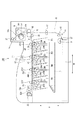
図1を参照し、画像形成装置の全体構成について概要説明する。図1は、本発明の実施例に係る画像形成装置の一態様であるカラーレーザープリンタ100の全体構成を示す縦断面図である。なお、画像形成装置としては、カラーレーザープリンタの他、複写機やファクシミリ等が挙げられる。
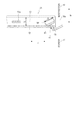
以下、露光装置3について説明する。図1(a)は、実施例1に係る露光装置3(ユニット)の斜視図であり、図1(b)はレーザ駆動基板45(ユニット基板)を正面から見た拡大図である。図1において、露光装置3の光学箱(筐体)40の内部構造の説明のために、カバー部材を取り外している。図2は、装置本体2のフレームと露光装置3の位置関係を表す図である。なお図2では、鉛直方向をH、水平方向において、左右方向をW、奥行き方向をDとしている。
実施例1では、露光装置3の小型化を図るため、露光装置3のレーザ駆動基板45に設けられたコネクタ46を、レーザ駆動基板45の長手方向に対してコネクタ46の長手方向が交差するように配置して構成としている。しかしながら本発明は、画像形成装置の内部に設けられたユニットを小型化するために用いることができ、適用範囲は露光装置3のレーザ駆動基板45に限らない。そこで本実施例では、本発明を画像形成装置100のセンサユニット23(ユニット)に適用した例について説明を行う。なお、本実施例に係る構成について説明では、実施例1と同様の構成については、同じ符号を付し、説明を省略し、差異点を中心に説明を行う。
3 露光装置(内部ユニット)
4 現像装置(現像ユニット)
7 プロセスカートリッジ
23 センサユニット(内部ユニット)
40 光学箱
41 半導体レーザ(光源)
42 偏向部材
43 入射光学系
44 結像光学系
44a 光学レンズ
44b ミラー
44c 光学レンズ
45 レーザ駆動基板
46 コネクタ
47 フレキシブルケーブル
49 制御基板
50 センサ基板(センサ50a)
51 金属部品
52 センサカバー
53 コネクタ
54 電線束
55 ネジ
100 画像形成装置
S 用紙
L 光ビーム
Claims (6)
- 画像形成動作を行うユニットと、
前記ユニットに設けられたユニット基板と、
前記ユニット基板に接続される配線と、
前記配線で前記第1の基板と接続され、前記ユニットを制御する制御基板と、
を備えた画像形成装置であって、
前記ユニット基板は、前記配線が接続されるコネクタを有し、
前記コネクタの長手方向は、前記ユニット基板の短手方向の長さに比べて長く、前記ユニット基板の短手方向と交差するように設けられている
ことを特徴とする画像形成装置。 - 前記ユニット基板の長手方向における一方の端部に前記コネクタが配置されており、前記ユニット基板の長手方向における、前記ユニット基板の前記一方に位置する辺は、前記コネクタの長手方向と略平行である
ことを特徴とする請求項1に記載の画像形成装置。 - 前記ユニット基板は、半導体レーザと、前記半導体レーザから出射されたレーザ光を偏向走査する偏向装置の駆動回路と、を含み、
前記ユニットは、前記偏向装置と、光学素子と、これらを内包した光学箱とを備えた光学走査装置である
ことを特徴とする請求項1または2に記載の画像形成装置。 - 前記配線は、フレキシブルケーブルであることを特徴とする請求項1乃至請求項3のいずれか1項に記載の画像形成装置。
- 画像形成動作に関する情報を取得するユニットと、
前記ユニットに設けられたユニット基板と、
前記ユニット基板に接続される配線と、
前記配線で前記第1の基板と接続され、前記ユニットを制御する制御基板と、
を備えた画像形成装置であって、
前記ユニット基板は、前記配線が接続されるコネクタを有し、
前記コネクタの長手方向は、前記ユニット基板の短手方向の長さに比べて長く、前記ユニット基板の短手方向と交差するように設けられている
ことを特徴とする画像形成装置。 - 前記ユニット基板は、半導体レーザと、前記半導体レーザから出射されたレーザ光を偏向走査する偏向装置の駆動回路と、を含み、
前記ユニットは、トナー画像の情報を取得するセンサユニットであって、
前記制御回路は、前記センサユニットの情報に基づいて、感光体ドラムを露光する露光装置を制御する
ことを特徴とする請求項5に記載の画像形成装置。
Priority Applications (5)
| Application Number | Priority Date | Filing Date | Title |
|---|---|---|---|
| JP2019102856A JP2020196169A (ja) | 2019-05-31 | 2019-05-31 | 画像形成装置 |
| US16/884,574 US11353804B2 (en) | 2019-05-31 | 2020-05-27 | Image forming apparatus |
| CN202010472899.2A CN112015075A (zh) | 2019-05-31 | 2020-05-29 | 成像设备 |
| US17/735,455 US20220260936A1 (en) | 2019-05-31 | 2022-05-03 | Image forming apparatus |
| JP2023182290A JP2023184582A (ja) | 2019-05-31 | 2023-10-24 | 画像形成装置 |
Applications Claiming Priority (1)
| Application Number | Priority Date | Filing Date | Title |
|---|---|---|---|
| JP2019102856A JP2020196169A (ja) | 2019-05-31 | 2019-05-31 | 画像形成装置 |
Related Child Applications (1)
| Application Number | Title | Priority Date | Filing Date |
|---|---|---|---|
| JP2023182290A Division JP2023184582A (ja) | 2019-05-31 | 2023-10-24 | 画像形成装置 |
Publications (2)
| Publication Number | Publication Date |
|---|---|
| JP2020196169A true JP2020196169A (ja) | 2020-12-10 |
| JP2020196169A5 JP2020196169A5 (ja) | 2022-05-19 |
Family
ID=73506293
Family Applications (2)
| Application Number | Title | Priority Date | Filing Date |
|---|---|---|---|
| JP2019102856A Pending JP2020196169A (ja) | 2019-05-31 | 2019-05-31 | 画像形成装置 |
| JP2023182290A Pending JP2023184582A (ja) | 2019-05-31 | 2023-10-24 | 画像形成装置 |
Family Applications After (1)
| Application Number | Title | Priority Date | Filing Date |
|---|---|---|---|
| JP2023182290A Pending JP2023184582A (ja) | 2019-05-31 | 2023-10-24 | 画像形成装置 |
Country Status (3)
| Country | Link |
|---|---|
| US (2) | US11353804B2 (ja) |
| JP (2) | JP2020196169A (ja) |
| CN (1) | CN112015075A (ja) |
Families Citing this family (2)
| Publication number | Priority date | Publication date | Assignee | Title |
|---|---|---|---|---|
| JP2020196169A (ja) * | 2019-05-31 | 2020-12-10 | キヤノン株式会社 | 画像形成装置 |
| JP2022122332A (ja) * | 2021-02-10 | 2022-08-23 | 京セラドキュメントソリューションズ株式会社 | 画像形成装置 |
Citations (9)
| Publication number | Priority date | Publication date | Assignee | Title |
|---|---|---|---|---|
| JPH06132057A (ja) * | 1992-10-14 | 1994-05-13 | Nippondenso Co Ltd | フレキシブルプリント配線板と回路基板との接続構造 |
| JPH11330656A (ja) * | 1998-05-18 | 1999-11-30 | Seiko Precision Inc | プリント基板の接合構造 |
| JP2001090156A (ja) * | 1999-09-27 | 2001-04-03 | Matsushita Electric Works Ltd | 局部洗浄装置 |
| JP2007301822A (ja) * | 2006-05-10 | 2007-11-22 | Brother Ind Ltd | 電子機器及び電子機器の製造方法 |
| JP2007305742A (ja) * | 2006-05-10 | 2007-11-22 | Sharp Corp | Led光源装置 |
| JP2009182294A (ja) * | 2008-02-01 | 2009-08-13 | Seiko Epson Corp | フレキシブル基板及びコネクタ、並びに電気光学装置及び電子機器 |
| JP2011197614A (ja) * | 2010-03-24 | 2011-10-06 | Brother Industries Ltd | 光走査装置 |
| JP2013033078A (ja) * | 2011-08-01 | 2013-02-14 | Fuji Xerox Co Ltd | 画像形成装置 |
| JP2014051011A (ja) * | 2012-09-06 | 2014-03-20 | Toshiba Tec Corp | 両面プリンタ装置 |
Family Cites Families (10)
| Publication number | Priority date | Publication date | Assignee | Title |
|---|---|---|---|---|
| JP3315917B2 (ja) * | 1998-01-23 | 2002-08-19 | 旭光学工業株式会社 | 光走査装置 |
| JP4223264B2 (ja) * | 2002-10-30 | 2009-02-12 | シャープ株式会社 | 離接機構および画像形成装置 |
| JP5268422B2 (ja) | 2008-05-09 | 2013-08-21 | キヤノン株式会社 | 画像形成装置 |
| JP4947177B2 (ja) * | 2010-03-25 | 2012-06-06 | ブラザー工業株式会社 | 画像読取装置 |
| JP6106382B2 (ja) * | 2012-08-24 | 2017-03-29 | シャープ株式会社 | 固体撮像素子およびその製造方法、電子情報機器 |
| JP6143059B2 (ja) * | 2012-11-12 | 2017-06-07 | 株式会社リコー | 給電装置、被給電ユニット及び画像形成装置 |
| JP2015139946A (ja) * | 2014-01-29 | 2015-08-03 | 富士ゼロックス株式会社 | 電子機器、露光装置及び画像形成装置 |
| JP2016163949A (ja) | 2015-03-06 | 2016-09-08 | 東レ株式会社 | 離型用保護ポリエステルフィルム |
| JP6403662B2 (ja) * | 2015-12-28 | 2018-10-10 | キヤノン株式会社 | 画像形成装置 |
| JP2020196169A (ja) * | 2019-05-31 | 2020-12-10 | キヤノン株式会社 | 画像形成装置 |
-
2019
- 2019-05-31 JP JP2019102856A patent/JP2020196169A/ja active Pending
-
2020
- 2020-05-27 US US16/884,574 patent/US11353804B2/en active Active
- 2020-05-29 CN CN202010472899.2A patent/CN112015075A/zh active Pending
-
2022
- 2022-05-03 US US17/735,455 patent/US20220260936A1/en active Pending
-
2023
- 2023-10-24 JP JP2023182290A patent/JP2023184582A/ja active Pending
Patent Citations (9)
| Publication number | Priority date | Publication date | Assignee | Title |
|---|---|---|---|---|
| JPH06132057A (ja) * | 1992-10-14 | 1994-05-13 | Nippondenso Co Ltd | フレキシブルプリント配線板と回路基板との接続構造 |
| JPH11330656A (ja) * | 1998-05-18 | 1999-11-30 | Seiko Precision Inc | プリント基板の接合構造 |
| JP2001090156A (ja) * | 1999-09-27 | 2001-04-03 | Matsushita Electric Works Ltd | 局部洗浄装置 |
| JP2007301822A (ja) * | 2006-05-10 | 2007-11-22 | Brother Ind Ltd | 電子機器及び電子機器の製造方法 |
| JP2007305742A (ja) * | 2006-05-10 | 2007-11-22 | Sharp Corp | Led光源装置 |
| JP2009182294A (ja) * | 2008-02-01 | 2009-08-13 | Seiko Epson Corp | フレキシブル基板及びコネクタ、並びに電気光学装置及び電子機器 |
| JP2011197614A (ja) * | 2010-03-24 | 2011-10-06 | Brother Industries Ltd | 光走査装置 |
| JP2013033078A (ja) * | 2011-08-01 | 2013-02-14 | Fuji Xerox Co Ltd | 画像形成装置 |
| JP2014051011A (ja) * | 2012-09-06 | 2014-03-20 | Toshiba Tec Corp | 両面プリンタ装置 |
Also Published As
| Publication number | Publication date |
|---|---|
| JP2023184582A (ja) | 2023-12-28 |
| US20200379355A1 (en) | 2020-12-03 |
| US11353804B2 (en) | 2022-06-07 |
| CN112015075A (zh) | 2020-12-01 |
| US20220260936A1 (en) | 2022-08-18 |
Similar Documents
| Publication | Publication Date | Title |
|---|---|---|
| US9316992B2 (en) | Light scanning apparatus and image forming apparatus | |
| US7821677B2 (en) | Method and apparatus for image forming capable of accurately detecting displacement of transfer images and image density | |
| US7873294B2 (en) | Image forming apparatus with increased noise resistance | |
| JP2023184582A (ja) | 画像形成装置 | |
| US8810833B2 (en) | Image processing device and image forming apparatus | |
| US10108125B2 (en) | Image forming apparatus | |
| JP7353778B2 (ja) | 画像形成装置 | |
| JP2004206070A (ja) | 電子写真装置 | |
| JP6739976B2 (ja) | 光学走査装置及び画像形成装置 | |
| CN110018622B (zh) | 电连接构造及图像形成装置 | |
| JP7190348B2 (ja) | 画像形成装置 | |
| JP6468166B2 (ja) | 内部ユニット、及び内部ユニットを備える画像形成装置 | |
| US9686430B2 (en) | Image reader, and image forming apparatus | |
| CN111830808B (zh) | 转印单元及图像形成装置 | |
| US20180034999A1 (en) | Exposure device and light receiving device | |
| JP2021056456A (ja) | トナー像形成ユニット及び画像形成装置 | |
| JP2020199672A (ja) | 光走査装置を備える画像形成装置 | |
| JP4413110B2 (ja) | 光書き込み装置及び画像形成装置 | |
| JP4545817B2 (ja) | 電子写真装置 | |
| JP2022025990A (ja) | 画像形成装置 | |
| JP2023070299A (ja) | 画像形成装置 | |
| JP2023049350A (ja) | 画像形成装置 | |
| JP2021124628A (ja) | 画像形成装置 | |
| JP2009192764A (ja) | 画像形成装置 | |
| JP2021056457A (ja) | 現像装置及び画像形成装置 |
Legal Events
| Date | Code | Title | Description |
|---|---|---|---|
| A521 | Request for written amendment filed |
Free format text: JAPANESE INTERMEDIATE CODE: A523 Effective date: 20220511 |
|
| A621 | Written request for application examination |
Free format text: JAPANESE INTERMEDIATE CODE: A621 Effective date: 20220511 |
|
| A977 | Report on retrieval |
Free format text: JAPANESE INTERMEDIATE CODE: A971007 Effective date: 20230201 |
|
| A131 | Notification of reasons for refusal |
Free format text: JAPANESE INTERMEDIATE CODE: A131 Effective date: 20230207 |
|
| A521 | Request for written amendment filed |
Free format text: JAPANESE INTERMEDIATE CODE: A523 Effective date: 20230403 |
|
| A131 | Notification of reasons for refusal |
Free format text: JAPANESE INTERMEDIATE CODE: A131 Effective date: 20230418 |
|
| A521 | Request for written amendment filed |
Free format text: JAPANESE INTERMEDIATE CODE: A523 Effective date: 20230609 |
|
| A02 | Decision of refusal |
Free format text: JAPANESE INTERMEDIATE CODE: A02 Effective date: 20230801 |