JP2016005002A - 太陽電池モジュール - Google Patents
太陽電池モジュール Download PDFInfo
- Publication number
- JP2016005002A JP2016005002A JP2015122060A JP2015122060A JP2016005002A JP 2016005002 A JP2016005002 A JP 2016005002A JP 2015122060 A JP2015122060 A JP 2015122060A JP 2015122060 A JP2015122060 A JP 2015122060A JP 2016005002 A JP2016005002 A JP 2016005002A
- Authority
- JP
- Japan
- Prior art keywords
- solar cell
- connector
- wiring
- electrode
- cell module
- Prior art date
- Legal status (The legal status is an assumption and is not a legal conclusion. Google has not performed a legal analysis and makes no representation as to the accuracy of the status listed.)
- Granted
Links
- 239000000758 substrate Substances 0.000 claims abstract description 87
- 239000004065 semiconductor Substances 0.000 claims abstract description 72
- 239000000853 adhesive Substances 0.000 claims abstract description 34
- 230000001070 adhesive effect Effects 0.000 claims abstract description 34
- 239000000463 material Substances 0.000 claims description 72
- 239000011248 coating agent Substances 0.000 abstract description 22
- 238000000576 coating method Methods 0.000 abstract description 22
- 239000007769 metal material Substances 0.000 description 19
- 239000010410 layer Substances 0.000 description 15
- 230000005684 electric field Effects 0.000 description 12
- 238000000034 method Methods 0.000 description 10
- 238000010586 diagram Methods 0.000 description 8
- 238000005452 bending Methods 0.000 description 6
- 239000010949 copper Substances 0.000 description 6
- 239000012792 core layer Substances 0.000 description 6
- 239000012535 impurity Substances 0.000 description 6
- 230000000644 propagated effect Effects 0.000 description 6
- 239000011247 coating layer Substances 0.000 description 5
- 238000005476 soldering Methods 0.000 description 5
- 238000002844 melting Methods 0.000 description 4
- 230000008018 melting Effects 0.000 description 4
- 239000002184 metal Substances 0.000 description 4
- 229910052751 metal Inorganic materials 0.000 description 4
- 238000010248 power generation Methods 0.000 description 4
- RYGMFSIKBFXOCR-UHFFFAOYSA-N Copper Chemical compound [Cu] RYGMFSIKBFXOCR-UHFFFAOYSA-N 0.000 description 3
- ATJFFYVFTNAWJD-UHFFFAOYSA-N Tin Chemical compound [Sn] ATJFFYVFTNAWJD-UHFFFAOYSA-N 0.000 description 3
- 229910052802 copper Inorganic materials 0.000 description 3
- 239000000945 filler Substances 0.000 description 3
- 238000009413 insulation Methods 0.000 description 3
- 238000004519 manufacturing process Methods 0.000 description 3
- 229910000679 solder Inorganic materials 0.000 description 3
- BQCADISMDOOEFD-UHFFFAOYSA-N Silver Chemical compound [Ag] BQCADISMDOOEFD-UHFFFAOYSA-N 0.000 description 2
- 230000000694 effects Effects 0.000 description 2
- 239000011810 insulating material Substances 0.000 description 2
- 239000002923 metal particle Substances 0.000 description 2
- 239000011347 resin Substances 0.000 description 2
- 229920005989 resin Polymers 0.000 description 2
- 229910052709 silver Inorganic materials 0.000 description 2
- 239000004332 silver Substances 0.000 description 2
- 239000000126 substance Substances 0.000 description 2
- 239000004593 Epoxy Substances 0.000 description 1
- XUIMIQQOPSSXEZ-UHFFFAOYSA-N Silicon Chemical compound [Si] XUIMIQQOPSSXEZ-UHFFFAOYSA-N 0.000 description 1
- 229910007637 SnAg Inorganic materials 0.000 description 1
- 229910008433 SnCU Inorganic materials 0.000 description 1
- 229910007116 SnPb Inorganic materials 0.000 description 1
- 239000002313 adhesive film Substances 0.000 description 1
- 229910045601 alloy Inorganic materials 0.000 description 1
- 239000000956 alloy Substances 0.000 description 1
- 229910052782 aluminium Inorganic materials 0.000 description 1
- 239000000470 constituent Substances 0.000 description 1
- 230000008602 contraction Effects 0.000 description 1
- 229910021419 crystalline silicon Inorganic materials 0.000 description 1
- 239000011521 glass Substances 0.000 description 1
- 229910052738 indium Inorganic materials 0.000 description 1
- APFVFJFRJDLVQX-UHFFFAOYSA-N indium atom Chemical compound [In] APFVFJFRJDLVQX-UHFFFAOYSA-N 0.000 description 1
- 239000011159 matrix material Substances 0.000 description 1
- 238000012986 modification Methods 0.000 description 1
- 230000004048 modification Effects 0.000 description 1
- 230000003287 optical effect Effects 0.000 description 1
- 238000002161 passivation Methods 0.000 description 1
- 230000000704 physical effect Effects 0.000 description 1
- 229920000642 polymer Polymers 0.000 description 1
- 238000005036 potential barrier Methods 0.000 description 1
- 238000005215 recombination Methods 0.000 description 1
- 230000006798 recombination Effects 0.000 description 1
- 238000000926 separation method Methods 0.000 description 1
- 229910052710 silicon Inorganic materials 0.000 description 1
- 239000010703 silicon Substances 0.000 description 1
- 239000002210 silicon-based material Substances 0.000 description 1
- 238000006467 substitution reaction Methods 0.000 description 1
Images


Classifications
-
- H—ELECTRICITY
- H01—ELECTRIC ELEMENTS
- H01L—SEMICONDUCTOR DEVICES NOT COVERED BY CLASS H10
- H01L31/00—Semiconductor devices sensitive to infrared radiation, light, electromagnetic radiation of shorter wavelength or corpuscular radiation and specially adapted either for the conversion of the energy of such radiation into electrical energy or for the control of electrical energy by such radiation; Processes or apparatus specially adapted for the manufacture or treatment thereof or of parts thereof; Details thereof
- H01L31/04—Semiconductor devices sensitive to infrared radiation, light, electromagnetic radiation of shorter wavelength or corpuscular radiation and specially adapted either for the conversion of the energy of such radiation into electrical energy or for the control of electrical energy by such radiation; Processes or apparatus specially adapted for the manufacture or treatment thereof or of parts thereof; Details thereof adapted as photovoltaic [PV] conversion devices
- H01L31/042—PV modules or arrays of single PV cells
- H01L31/05—Electrical interconnection means between PV cells inside the PV module, e.g. series connection of PV cells
- H01L31/0504—Electrical interconnection means between PV cells inside the PV module, e.g. series connection of PV cells specially adapted for series or parallel connection of solar cells in a module
- H01L31/0512—Electrical interconnection means between PV cells inside the PV module, e.g. series connection of PV cells specially adapted for series or parallel connection of solar cells in a module made of a particular material or composition of materials
-
- H—ELECTRICITY
- H01—ELECTRIC ELEMENTS
- H01L—SEMICONDUCTOR DEVICES NOT COVERED BY CLASS H10
- H01L31/00—Semiconductor devices sensitive to infrared radiation, light, electromagnetic radiation of shorter wavelength or corpuscular radiation and specially adapted either for the conversion of the energy of such radiation into electrical energy or for the control of electrical energy by such radiation; Processes or apparatus specially adapted for the manufacture or treatment thereof or of parts thereof; Details thereof
- H01L31/04—Semiconductor devices sensitive to infrared radiation, light, electromagnetic radiation of shorter wavelength or corpuscular radiation and specially adapted either for the conversion of the energy of such radiation into electrical energy or for the control of electrical energy by such radiation; Processes or apparatus specially adapted for the manufacture or treatment thereof or of parts thereof; Details thereof adapted as photovoltaic [PV] conversion devices
- H01L31/042—PV modules or arrays of single PV cells
- H01L31/05—Electrical interconnection means between PV cells inside the PV module, e.g. series connection of PV cells
- H01L31/0504—Electrical interconnection means between PV cells inside the PV module, e.g. series connection of PV cells specially adapted for series or parallel connection of solar cells in a module
- H01L31/0516—Electrical interconnection means between PV cells inside the PV module, e.g. series connection of PV cells specially adapted for series or parallel connection of solar cells in a module specially adapted for interconnection of back-contact solar cells
-
- H—ELECTRICITY
- H01—ELECTRIC ELEMENTS
- H01L—SEMICONDUCTOR DEVICES NOT COVERED BY CLASS H10
- H01L31/00—Semiconductor devices sensitive to infrared radiation, light, electromagnetic radiation of shorter wavelength or corpuscular radiation and specially adapted either for the conversion of the energy of such radiation into electrical energy or for the control of electrical energy by such radiation; Processes or apparatus specially adapted for the manufacture or treatment thereof or of parts thereof; Details thereof
- H01L31/02—Details
- H01L31/02002—Arrangements for conducting electric current to or from the device in operations
- H01L31/02005—Arrangements for conducting electric current to or from the device in operations for device characterised by at least one potential jump barrier or surface barrier
- H01L31/02008—Arrangements for conducting electric current to or from the device in operations for device characterised by at least one potential jump barrier or surface barrier for solar cells or solar cell modules
- H01L31/0201—Arrangements for conducting electric current to or from the device in operations for device characterised by at least one potential jump barrier or surface barrier for solar cells or solar cell modules comprising specially adapted module bus-bar structures
-
- H—ELECTRICITY
- H01—ELECTRIC ELEMENTS
- H01L—SEMICONDUCTOR DEVICES NOT COVERED BY CLASS H10
- H01L31/00—Semiconductor devices sensitive to infrared radiation, light, electromagnetic radiation of shorter wavelength or corpuscular radiation and specially adapted either for the conversion of the energy of such radiation into electrical energy or for the control of electrical energy by such radiation; Processes or apparatus specially adapted for the manufacture or treatment thereof or of parts thereof; Details thereof
- H01L31/02—Details
- H01L31/02016—Circuit arrangements of general character for the devices
- H01L31/02019—Circuit arrangements of general character for the devices for devices characterised by at least one potential jump barrier or surface barrier
- H01L31/02021—Circuit arrangements of general character for the devices for devices characterised by at least one potential jump barrier or surface barrier for solar cells
-
- H—ELECTRICITY
- H01—ELECTRIC ELEMENTS
- H01L—SEMICONDUCTOR DEVICES NOT COVERED BY CLASS H10
- H01L31/00—Semiconductor devices sensitive to infrared radiation, light, electromagnetic radiation of shorter wavelength or corpuscular radiation and specially adapted either for the conversion of the energy of such radiation into electrical energy or for the control of electrical energy by such radiation; Processes or apparatus specially adapted for the manufacture or treatment thereof or of parts thereof; Details thereof
- H01L31/02—Details
- H01L31/0224—Electrodes
- H01L31/022408—Electrodes for devices characterised by at least one potential jump barrier or surface barrier
- H01L31/022425—Electrodes for devices characterised by at least one potential jump barrier or surface barrier for solar cells
- H01L31/022441—Electrode arrangements specially adapted for back-contact solar cells
-
- H—ELECTRICITY
- H01—ELECTRIC ELEMENTS
- H01L—SEMICONDUCTOR DEVICES NOT COVERED BY CLASS H10
- H01L31/00—Semiconductor devices sensitive to infrared radiation, light, electromagnetic radiation of shorter wavelength or corpuscular radiation and specially adapted either for the conversion of the energy of such radiation into electrical energy or for the control of electrical energy by such radiation; Processes or apparatus specially adapted for the manufacture or treatment thereof or of parts thereof; Details thereof
- H01L31/04—Semiconductor devices sensitive to infrared radiation, light, electromagnetic radiation of shorter wavelength or corpuscular radiation and specially adapted either for the conversion of the energy of such radiation into electrical energy or for the control of electrical energy by such radiation; Processes or apparatus specially adapted for the manufacture or treatment thereof or of parts thereof; Details thereof adapted as photovoltaic [PV] conversion devices
- H01L31/042—PV modules or arrays of single PV cells
- H01L31/05—Electrical interconnection means between PV cells inside the PV module, e.g. series connection of PV cells
- H01L31/0504—Electrical interconnection means between PV cells inside the PV module, e.g. series connection of PV cells specially adapted for series or parallel connection of solar cells in a module
-
- H—ELECTRICITY
- H01—ELECTRIC ELEMENTS
- H01L—SEMICONDUCTOR DEVICES NOT COVERED BY CLASS H10
- H01L31/00—Semiconductor devices sensitive to infrared radiation, light, electromagnetic radiation of shorter wavelength or corpuscular radiation and specially adapted either for the conversion of the energy of such radiation into electrical energy or for the control of electrical energy by such radiation; Processes or apparatus specially adapted for the manufacture or treatment thereof or of parts thereof; Details thereof
- H01L31/04—Semiconductor devices sensitive to infrared radiation, light, electromagnetic radiation of shorter wavelength or corpuscular radiation and specially adapted either for the conversion of the energy of such radiation into electrical energy or for the control of electrical energy by such radiation; Processes or apparatus specially adapted for the manufacture or treatment thereof or of parts thereof; Details thereof adapted as photovoltaic [PV] conversion devices
- H01L31/06—Semiconductor devices sensitive to infrared radiation, light, electromagnetic radiation of shorter wavelength or corpuscular radiation and specially adapted either for the conversion of the energy of such radiation into electrical energy or for the control of electrical energy by such radiation; Processes or apparatus specially adapted for the manufacture or treatment thereof or of parts thereof; Details thereof adapted as photovoltaic [PV] conversion devices characterised by at least one potential-jump barrier or surface barrier
- H01L31/068—Semiconductor devices sensitive to infrared radiation, light, electromagnetic radiation of shorter wavelength or corpuscular radiation and specially adapted either for the conversion of the energy of such radiation into electrical energy or for the control of electrical energy by such radiation; Processes or apparatus specially adapted for the manufacture or treatment thereof or of parts thereof; Details thereof adapted as photovoltaic [PV] conversion devices characterised by at least one potential-jump barrier or surface barrier the potential barriers being only of the PN homojunction type, e.g. bulk silicon PN homojunction solar cells or thin film polycrystalline silicon PN homojunction solar cells
- H01L31/0682—Semiconductor devices sensitive to infrared radiation, light, electromagnetic radiation of shorter wavelength or corpuscular radiation and specially adapted either for the conversion of the energy of such radiation into electrical energy or for the control of electrical energy by such radiation; Processes or apparatus specially adapted for the manufacture or treatment thereof or of parts thereof; Details thereof adapted as photovoltaic [PV] conversion devices characterised by at least one potential-jump barrier or surface barrier the potential barriers being only of the PN homojunction type, e.g. bulk silicon PN homojunction solar cells or thin film polycrystalline silicon PN homojunction solar cells back-junction, i.e. rearside emitter, solar cells, e.g. interdigitated base-emitter regions back-junction cells
-
- Y—GENERAL TAGGING OF NEW TECHNOLOGICAL DEVELOPMENTS; GENERAL TAGGING OF CROSS-SECTIONAL TECHNOLOGIES SPANNING OVER SEVERAL SECTIONS OF THE IPC; TECHNICAL SUBJECTS COVERED BY FORMER USPC CROSS-REFERENCE ART COLLECTIONS [XRACs] AND DIGESTS
- Y02—TECHNOLOGIES OR APPLICATIONS FOR MITIGATION OR ADAPTATION AGAINST CLIMATE CHANGE
- Y02E—REDUCTION OF GREENHOUSE GAS [GHG] EMISSIONS, RELATED TO ENERGY GENERATION, TRANSMISSION OR DISTRIBUTION
- Y02E10/00—Energy generation through renewable energy sources
- Y02E10/50—Photovoltaic [PV] energy
- Y02E10/52—PV systems with concentrators
-
- Y—GENERAL TAGGING OF NEW TECHNOLOGICAL DEVELOPMENTS; GENERAL TAGGING OF CROSS-SECTIONAL TECHNOLOGIES SPANNING OVER SEVERAL SECTIONS OF THE IPC; TECHNICAL SUBJECTS COVERED BY FORMER USPC CROSS-REFERENCE ART COLLECTIONS [XRACs] AND DIGESTS
- Y02—TECHNOLOGIES OR APPLICATIONS FOR MITIGATION OR ADAPTATION AGAINST CLIMATE CHANGE
- Y02E—REDUCTION OF GREENHOUSE GAS [GHG] EMISSIONS, RELATED TO ENERGY GENERATION, TRANSMISSION OR DISTRIBUTION
- Y02E10/00—Energy generation through renewable energy sources
- Y02E10/50—Photovoltaic [PV] energy
- Y02E10/547—Monocrystalline silicon PV cells
Abstract
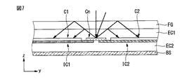
【解決手段】本発明に係る太陽電池モジュールは、半導体基板と、半導体基板に形成され、異なる導電性電荷を収集する第1電極と第2電極を含む複数の太陽電池と、複数の太陽電池の内で互いに隣接した第1太陽電池と第2太陽電池の第1電極と第2電極に接続された複数の配線であって、第1太陽電池と第2太陽電池の直列接続のために導電性接着剤で接続し、第1太陽電池と第2太陽電池の第1電極と第2電極から絶縁層で絶縁される複数の配線と、第1太陽電池と第2太陽電池間に位置して複数の配線に接続されているコネクタを含み、コネクタの幅は、第1太陽電池とコネクタの間の第1距離または第2太陽電池とコネクタとの間の第2距離の内の少なくとも一つと同じか大きく、コネクタ上の絶縁層の塗布面積は、コネクタ上の導電性接着剤の塗布面積よりも大きい。
【選択図】図1
Description
以下では添付した図面を参照して本発明の実施の形態に対して本発明が属する技術分野で通常の知識を有する者が容易に実施できるように詳しく説明する。しかし本発明はいろいろ多様な形態に具現されることができここで説明する実施の形態に限定されない。そして図面で本発明を明確に説明するために説明と関係ない部分は省略し、明細書全体を介して類似の部分に対しては類似の図面符号を付けた。
Claims (22)
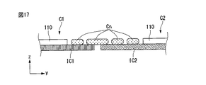
- 半導体基板と、前記半導体基板に形成され、異なる導電性電荷を収集する第1電極と第2電極を含む複数の太陽電池と、
前記複数の太陽電池の内で互いに隣接した第1太陽電池と第2太陽電池の前記第1電極と前記第2電極に接続された複数の配線であって、前記第1太陽電池と前記第2太陽電池の直列接続のために導電性接着剤で接続し、又は、前記第1太陽電池と第2太陽電池の前記第1電極と第2電極から絶縁層で絶縁される複数の配線と、
前記第1太陽電池と前記第2太陽電池との間に位置して前記複数の配線に接続されるコネクタを含み、
前記コネクタの幅は、前記第1太陽電池と前記コネクタとの間の第1距離又は前記第2太陽電池と前記コネクタとの間の第2距離の内の少なくとも一つと同じか大きく、
前記コネクタ上の前記絶縁層の塗布面積は、前記コネクタ上の前記導電性接着剤の塗布面積より大きい、太陽電池モジュール。 - 各配線の先端と前記コネクタとの重畳領域は、前記コネクタの幅と同じか狭い、請求項1に記載の太陽電池モジュール。
- 前記各配線の先端と前記コネクタとの重畳領域は、前記コネクタの幅×1/3と同じか大きい、請求項2に記載の太陽電池モジュール。
- 前記コネクタは、光が入射する第1面と前記第1面と反対の第2面を含み、前記複数の配線のすべては、前記コネクタの前記第2面に接続される、請求項2に記載の太陽電池モジュール。
- 前記コネクタの前記第1面は、互いに傾斜面の角度が異なる複数の凹凸を含む、請求項3に記載の太陽電池モジュール。
- 前記コネクタの前記第2面は、前記複数の配線を形成する物質の少なくとも1つと同一の物質を含む、請求項4に記載の太陽電池モジュール。
- 前記コネクタの前記第1面を形成する物質は、前記コネクタの前記第2面を形成する物質と異なる、請求項5に記載の太陽電池モジュール。
- 前記コネクタの長さは、前記複数の配線の内、最初と最後に位置する二つの配線間の距離と同じかより大きく、前記第1太陽電池の幅と前記複数の太陽電池のストリングの間の間隔の合計より小さい、請求項2に記載の太陽電池モジュール。
- 前記コネクタの中心の幅は、前記コネクタの端の幅より小さい、請求項8に記載の太陽電池モジュール。
- 前記コネクタの端の幅と前記コネクタの中心の幅の差の最大値は、10mmである、請求項9に記載の太陽電池モジュール。
- 前記第1電極と前記第2電極は、前記半導体基板の後面に互いに並行に交互に形成され、
前記複数の配線は、
前記第1太陽電池の第1電極を前記第2太陽電池の第2電極に接続させる第1配線と、前記第1太陽電池の第2電極を前記第2太陽電池の第1電極に接続させる第2配線を含む、請求項1に記載の太陽電池モジュール。 - 前記第1配線は、前記第1太陽電池の第1電極と前記第2太陽電池の第2電極に導電性接着剤で接続され、前記第1太陽電池の第2電極及び前記第2太陽電池の第1電極から絶縁層で絶縁され、
前記第2配線は、前記第1太陽電池の第2電極と前記第2太陽電池の第1電極に導電性接着剤で接続され、前記第1太陽電池の第1電極及び前記第2太陽電池の第2電極から絶縁層で絶縁される、請求項11に記載の太陽電池モジュール。 - 前記第1配線と前記第2配線は互いに、前記コネクタにおいて、前記コネクタの幅と同じか、小さい距離で対面する、請求項11に記載の太陽電池モジュール。
- 前記コネクタによって互に接続されて列を成す複数の太陽電池からなる複数のストリングと、
前記複数のストリングの中で、互いに隣接する第1ストリングと第2ストリングを接続するブッシング バーを含み、
前記コネクタの断面積は、前記ブッシング バーの断面積よりも小さい、請求項2に記載の太陽電池モジュール。 - 前記ブッシング バーの形成物質、前記コネクタの形成物質、及び前記複数の配線の形成物質は、少なくとも1つ以上の物質を共通に含む、請求項14に記載の太陽電池モジュール。
- 前記ブッシング バーは、光が入射する第1面と前記第1面と反対の第2面を含み、
前記ブッシング バーに接続された前記複数の配線は、前記ブッシングバーの前記第2面に接続され、
前記ブシッングバーの前記第1面は互いに傾斜面の角度が異なり、一方向に傾く、複数の凹凸を含む、請求項14に記載の太陽電池モジュール。 - 前記第1太陽電池と前記コネクタとの間の間隔及び、前記第2太陽電池と前記コネクタとの間の間隔は、50μm〜3mmである、請求項1に記載の太陽電池モジュール。
- 前記コネクタの幅は、0.1mm〜20mmであり、前記コネクタの厚さは0.015mm〜2mmである、請求項17に記載の太陽電池モジュール。
- 前記コネクタの厚さは、前記第1太陽電池または前記第2太陽電池の内の少なくとも一つの厚さより厚い、請求項1に記載の太陽電池モジュール。
- 前記コネクタの厚さは、前記第1配線又は前記第2配線の内の少なくとも一つの厚さと同じかより薄い、請求項1に記載の太陽電池モジュール。
- 前記第1配線の断面積は、前記第2配線の断面積と異なる、請求項11に記載の太陽電池モジュール。
- 前記第1太陽電池の第1電極の断面積は、前記第2太陽電池の第1電極の断面積より小さく、前記第1配線の断面積は、前記第2配線の断面積より大きい、請求項21に記載の太陽電池モジュール。
Applications Claiming Priority (4)
| Application Number | Priority Date | Filing Date | Title |
|---|---|---|---|
| KR1020140074609A KR102244597B1 (ko) | 2014-06-18 | 2014-06-18 | 태양 전지 모듈 |
| KR10-2014-0074609 | 2014-06-18 | ||
| KR1020140128553A KR102273018B1 (ko) | 2014-09-25 | 2014-09-25 | 태양 전지 모듈 |
| KR10-2014-0128553 | 2014-09-25 |
Related Child Applications (1)
| Application Number | Title | Priority Date | Filing Date |
|---|---|---|---|
| JP2017172283A Division JP6382414B2 (ja) | 2014-06-18 | 2017-09-07 | 太陽電池モジュール |
Publications (2)
| Publication Number | Publication Date |
|---|---|
| JP2016005002A true JP2016005002A (ja) | 2016-01-12 |
| JP6208714B2 JP6208714B2 (ja) | 2017-10-04 |
Family
ID=53434179
Family Applications (2)
| Application Number | Title | Priority Date | Filing Date |
|---|---|---|---|
| JP2015122060A Active JP6208714B2 (ja) | 2014-06-18 | 2015-06-17 | 太陽電池モジュール |
| JP2017172283A Active JP6382414B2 (ja) | 2014-06-18 | 2017-09-07 | 太陽電池モジュール |
Family Applications After (1)
| Application Number | Title | Priority Date | Filing Date |
|---|---|---|---|
| JP2017172283A Active JP6382414B2 (ja) | 2014-06-18 | 2017-09-07 | 太陽電池モジュール |
Country Status (4)
| Country | Link |
|---|---|
| US (1) | US10483421B2 (ja) |
| EP (1) | EP2958152B1 (ja) |
| JP (2) | JP6208714B2 (ja) |
| CN (1) | CN105206696B (ja) |
Cited By (12)
| Publication number | Priority date | Publication date | Assignee | Title |
|---|---|---|---|---|
| JP2017201691A (ja) * | 2016-05-03 | 2017-11-09 | エルジー エレクトロニクス インコーポレイティド | 太陽電池モジュール |
| JP2017228629A (ja) * | 2016-06-22 | 2017-12-28 | シャープ株式会社 | 太陽電池モジュール |
| KR101806972B1 (ko) * | 2016-07-21 | 2018-01-18 | 엘지전자 주식회사 | 태양 전지 모듈 |
| KR101806971B1 (ko) * | 2016-08-26 | 2018-01-18 | 엘지전자 주식회사 | 태양 전지 모듈의 제조 방법과 그에 의한 태양 전지 모듈 |
| JP2018032859A (ja) * | 2016-08-26 | 2018-03-01 | エルジー エレクトロニクス インコーポレイティド | 太陽電池モジュールの製造方法及びそれに従う太陽電池モジュール |
| JP2018046112A (ja) * | 2016-09-13 | 2018-03-22 | パナソニックIpマネジメント株式会社 | 太陽電池モジュール |
| JP2018056490A (ja) * | 2016-09-30 | 2018-04-05 | パナソニックIpマネジメント株式会社 | 太陽電池モジュールおよび太陽電池セル |
| WO2020066395A1 (ja) * | 2018-09-28 | 2020-04-02 | パナソニック株式会社 | 太陽電池モジュールの製造方法および太陽電池モジュール |
| JP2020057652A (ja) * | 2018-09-28 | 2020-04-09 | パナソニック株式会社 | 太陽電池モジュールおよび太陽電池モジュールの製造方法 |
| JP2020061551A (ja) * | 2018-10-05 | 2020-04-16 | エルジー エレクトロニクス インコーポレイティド | 太陽電池パネル |
| US11652178B2 (en) | 2018-12-27 | 2023-05-16 | Panasonic Holdings Corporation | Solar cell module including solar cells |
| JP7446481B2 (ja) | 2020-04-29 | 2024-03-08 | シャンラオ シンユエン ユエドン テクノロジー デベロップメント シーオー.,エルティーディー | 太陽電池パネル及びその製造方法 |
Families Citing this family (11)
| Publication number | Priority date | Publication date | Assignee | Title |
|---|---|---|---|---|
| KR20150100146A (ko) * | 2014-02-24 | 2015-09-02 | 엘지전자 주식회사 | 태양 전지 모듈 |
| KR101820103B1 (ko) * | 2014-10-27 | 2018-01-18 | 엘지전자 주식회사 | 태양전지 모듈, 그 리페어 방법 및 리페어 장치 |
| JP6352894B2 (ja) | 2015-12-24 | 2018-07-04 | トヨタ自動車株式会社 | 太陽電池モジュール |
| EP3655998A1 (en) * | 2017-07-20 | 2020-05-27 | Meyer Burger (Switzerland) AG | Stabilized shingled solar cell strings and methods for their production |
| CN108010981A (zh) * | 2017-12-28 | 2018-05-08 | 常州华威新材料有限公司 | 提高光伏转换效率的反光膜及其制备方法 |
| KR102600380B1 (ko) | 2018-12-05 | 2023-11-09 | 상라오 징코 솔라 테크놀러지 디벨롭먼트 컴퍼니, 리미티드 | 태양 전지 및 이의 제조 방법, 그리고 태양 전지 패널 |
| CN109950334B (zh) * | 2019-04-02 | 2024-03-26 | 晶澳(扬州)太阳能科技有限公司 | Mwt太阳能电池组串及其制备方法、组件 |
| US11791431B2 (en) | 2021-05-28 | 2023-10-17 | Zhejiang Aiko Solar Energy Technology Co., Ltd. | Back contact solar cell string and preparation method therefor, module, and system |
| CN113193058A (zh) * | 2021-05-28 | 2021-07-30 | 浙江爱旭太阳能科技有限公司 | 一种背接触太阳能电池串及制备方法、组件及系统 |
| CN113327997A (zh) * | 2021-07-15 | 2021-08-31 | 浙江爱旭太阳能科技有限公司 | 一种背接触太阳能电池串及制备方法、组件及系统 |
| EP4125137A1 (en) * | 2021-07-28 | 2023-02-01 | Meyer Burger (Switzerland) AG | Solar cell module |
Citations (8)
| Publication number | Priority date | Publication date | Assignee | Title |
|---|---|---|---|---|
| WO2008090718A1 (ja) * | 2007-01-25 | 2008-07-31 | Sharp Kabushiki Kaisha | 太陽電池セル、太陽電池アレイおよび太陽電池モジュールならびに太陽電池アレイの製造方法 |
| WO2009025147A1 (ja) * | 2007-08-23 | 2009-02-26 | Sharp Kabushiki Kaisha | 裏面接合型太陽電池、配線基板付き裏面接合型太陽電池、太陽電池ストリングおよび太陽電池モジュール |
| US20100139746A1 (en) * | 2007-03-19 | 2010-06-10 | Q-Cells Se | Solar cell device, solar cell module, and connector device |
| JP2011003724A (ja) * | 2009-06-18 | 2011-01-06 | Sanyo Electric Co Ltd | 太陽電池モジュール |
| JP2012074414A (ja) * | 2010-09-27 | 2012-04-12 | Sanyo Electric Co Ltd | 太陽電池モジュール及びその製造方法 |
| JP2013008785A (ja) * | 2011-06-23 | 2013-01-10 | Sanyo Electric Co Ltd | 太陽電池モジュール |
| WO2013168612A1 (ja) * | 2012-05-09 | 2013-11-14 | 三洋電機株式会社 | 太陽電池モジュール |
| JP2014007384A (ja) * | 2012-06-22 | 2014-01-16 | Lg Electronics Inc | 太陽電池モジュール及びそれに適用されるリボン結合体 |
Family Cites Families (6)
| Publication number | Priority date | Publication date | Assignee | Title |
|---|---|---|---|---|
| DE102008044910A1 (de) | 2008-08-30 | 2010-03-04 | Fraunhofer-Gesellschaft zur Förderung der angewandten Forschung e.V. | Solarzelle und Solarzellenmodul mit einseitiger Verschaltung |
| KR101284278B1 (ko) | 2011-04-12 | 2013-07-08 | 엘지전자 주식회사 | 태양 전지 모듈 및 태양 전지 모듈에 사용되는 인터커넥터 |
| KR101231314B1 (ko) | 2011-05-25 | 2013-02-07 | 현대중공업 주식회사 | 태양전지 모듈 |
| KR102319721B1 (ko) | 2013-10-29 | 2021-11-01 | 엘지전자 주식회사 | 태양 전지 및 태양 전지 모듈 |
| KR102175893B1 (ko) | 2014-02-24 | 2020-11-06 | 엘지전자 주식회사 | 태양 전지 모듈의 제조 방법 |
| KR20150100146A (ko) | 2014-02-24 | 2015-09-02 | 엘지전자 주식회사 | 태양 전지 모듈 |
-
2015
- 2015-06-17 US US14/742,478 patent/US10483421B2/en active Active
- 2015-06-17 EP EP15001796.0A patent/EP2958152B1/en active Active
- 2015-06-17 JP JP2015122060A patent/JP6208714B2/ja active Active
- 2015-06-18 CN CN201510341156.0A patent/CN105206696B/zh active Active
-
2017
- 2017-09-07 JP JP2017172283A patent/JP6382414B2/ja active Active
Patent Citations (8)
| Publication number | Priority date | Publication date | Assignee | Title |
|---|---|---|---|---|
| WO2008090718A1 (ja) * | 2007-01-25 | 2008-07-31 | Sharp Kabushiki Kaisha | 太陽電池セル、太陽電池アレイおよび太陽電池モジュールならびに太陽電池アレイの製造方法 |
| US20100139746A1 (en) * | 2007-03-19 | 2010-06-10 | Q-Cells Se | Solar cell device, solar cell module, and connector device |
| WO2009025147A1 (ja) * | 2007-08-23 | 2009-02-26 | Sharp Kabushiki Kaisha | 裏面接合型太陽電池、配線基板付き裏面接合型太陽電池、太陽電池ストリングおよび太陽電池モジュール |
| JP2011003724A (ja) * | 2009-06-18 | 2011-01-06 | Sanyo Electric Co Ltd | 太陽電池モジュール |
| JP2012074414A (ja) * | 2010-09-27 | 2012-04-12 | Sanyo Electric Co Ltd | 太陽電池モジュール及びその製造方法 |
| JP2013008785A (ja) * | 2011-06-23 | 2013-01-10 | Sanyo Electric Co Ltd | 太陽電池モジュール |
| WO2013168612A1 (ja) * | 2012-05-09 | 2013-11-14 | 三洋電機株式会社 | 太陽電池モジュール |
| JP2014007384A (ja) * | 2012-06-22 | 2014-01-16 | Lg Electronics Inc | 太陽電池モジュール及びそれに適用されるリボン結合体 |
Cited By (19)
| Publication number | Priority date | Publication date | Assignee | Title |
|---|---|---|---|---|
| JP2017201691A (ja) * | 2016-05-03 | 2017-11-09 | エルジー エレクトロニクス インコーポレイティド | 太陽電池モジュール |
| JP7004513B2 (ja) | 2016-05-03 | 2022-01-21 | エルジー エレクトロニクス インコーポレイティド | 太陽電池モジュール |
| JP2017228629A (ja) * | 2016-06-22 | 2017-12-28 | シャープ株式会社 | 太陽電池モジュール |
| KR101806972B1 (ko) * | 2016-07-21 | 2018-01-18 | 엘지전자 주식회사 | 태양 전지 모듈 |
| JP2018032859A (ja) * | 2016-08-26 | 2018-03-01 | エルジー エレクトロニクス インコーポレイティド | 太陽電池モジュールの製造方法及びそれに従う太陽電池モジュール |
| US10700228B2 (en) | 2016-08-26 | 2020-06-30 | Lg Electronics Inc. | Method for manufacturing solar cell module having defect tested solar cell strings |
| KR101806971B1 (ko) * | 2016-08-26 | 2018-01-18 | 엘지전자 주식회사 | 태양 전지 모듈의 제조 방법과 그에 의한 태양 전지 모듈 |
| JP2018046112A (ja) * | 2016-09-13 | 2018-03-22 | パナソニックIpマネジメント株式会社 | 太陽電池モジュール |
| JP2018056490A (ja) * | 2016-09-30 | 2018-04-05 | パナソニックIpマネジメント株式会社 | 太陽電池モジュールおよび太陽電池セル |
| CN112753107A (zh) * | 2018-09-28 | 2021-05-04 | 松下电器产业株式会社 | 太阳能电池模块的制造方法及太阳能电池模块 |
| JP2020057652A (ja) * | 2018-09-28 | 2020-04-09 | パナソニック株式会社 | 太陽電池モジュールおよび太陽電池モジュールの製造方法 |
| WO2020066395A1 (ja) * | 2018-09-28 | 2020-04-02 | パナソニック株式会社 | 太陽電池モジュールの製造方法および太陽電池モジュール |
| US11581455B2 (en) | 2018-09-28 | 2023-02-14 | Panasonic Holdings Corporation | Solar cell module manufacturing method and solar cell module |
| CN112753107B (zh) * | 2018-09-28 | 2023-06-30 | 松下控股株式会社 | 太阳能电池模块的制造方法及太阳能电池模块 |
| JP7317479B2 (ja) | 2018-09-28 | 2023-07-31 | パナソニックホールディングス株式会社 | 太陽電池モジュールおよび太陽電池モジュールの製造方法 |
| JP2020061551A (ja) * | 2018-10-05 | 2020-04-16 | エルジー エレクトロニクス インコーポレイティド | 太陽電池パネル |
| US11810991B2 (en) | 2018-10-05 | 2023-11-07 | Lg Electronics Inc. | Solar cell panel |
| US11652178B2 (en) | 2018-12-27 | 2023-05-16 | Panasonic Holdings Corporation | Solar cell module including solar cells |
| JP7446481B2 (ja) | 2020-04-29 | 2024-03-08 | シャンラオ シンユエン ユエドン テクノロジー デベロップメント シーオー.,エルティーディー | 太陽電池パネル及びその製造方法 |
Also Published As
| Publication number | Publication date |
|---|---|
| EP2958152B1 (en) | 2021-04-21 |
| EP2958152A1 (en) | 2015-12-23 |
| US10483421B2 (en) | 2019-11-19 |
| CN105206696B (zh) | 2017-05-24 |
| CN105206696A (zh) | 2015-12-30 |
| JP6208714B2 (ja) | 2017-10-04 |
| JP6382414B2 (ja) | 2018-08-29 |
| US20150372177A1 (en) | 2015-12-24 |
| JP2018011073A (ja) | 2018-01-18 |
Similar Documents
| Publication | Publication Date | Title |
|---|---|---|
| JP6382414B2 (ja) | 太陽電池モジュール | |
| JP6082039B2 (ja) | 太陽電池モジュール | |
| JP7432571B2 (ja) | 太陽電池モジュールとその製造方法 | |
| JP6665221B2 (ja) | 太陽電池モジュール | |
| JP6307131B2 (ja) | 太陽電池モジュール及びその製造方法 | |
| JP6835800B2 (ja) | 太陽電池モジュール | |
| JP6139581B2 (ja) | 太陽電池モジュール | |
| KR102244597B1 (ko) | 태양 전지 모듈 | |
| JP7129786B2 (ja) | 構造を改善した太陽電池及びこれを用いた太陽電池モジュール | |
| JP7004513B2 (ja) | 太陽電池モジュール | |
| JP6373919B2 (ja) | 太陽電池モジュール | |
| KR102219791B1 (ko) | 태양 전지 모듈 | |
| KR101714778B1 (ko) | 태양 전지 모듈 | |
| KR102374145B1 (ko) | 태양 전지 패널 | |
| JP2011249736A (ja) | 太陽電池モジュールの製造方法 | |
| KR102233873B1 (ko) | 태양 전지 모듈 |
Legal Events
| Date | Code | Title | Description |
|---|---|---|---|
| A977 | Report on retrieval |
Free format text: JAPANESE INTERMEDIATE CODE: A971007 Effective date: 20160428 |
|
| A131 | Notification of reasons for refusal |
Free format text: JAPANESE INTERMEDIATE CODE: A131 Effective date: 20160510 |
|
| A521 | Request for written amendment filed |
Free format text: JAPANESE INTERMEDIATE CODE: A523 Effective date: 20160809 |
|
| A131 | Notification of reasons for refusal |
Free format text: JAPANESE INTERMEDIATE CODE: A131 Effective date: 20170110 |
|
| A521 | Request for written amendment filed |
Free format text: JAPANESE INTERMEDIATE CODE: A523 Effective date: 20170330 |
|
| TRDD | Decision of grant or rejection written | ||
| A01 | Written decision to grant a patent or to grant a registration (utility model) |
Free format text: JAPANESE INTERMEDIATE CODE: A01 Effective date: 20170808 |
|
| A61 | First payment of annual fees (during grant procedure) |
Free format text: JAPANESE INTERMEDIATE CODE: A61 Effective date: 20170907 |
|
| R150 | Certificate of patent or registration of utility model |
Ref document number: 6208714 Country of ref document: JP Free format text: JAPANESE INTERMEDIATE CODE: R150 |
|
| R250 | Receipt of annual fees |
Free format text: JAPANESE INTERMEDIATE CODE: R250 |
|
| R250 | Receipt of annual fees |
Free format text: JAPANESE INTERMEDIATE CODE: R250 |
|
| R250 | Receipt of annual fees |
Free format text: JAPANESE INTERMEDIATE CODE: R250 |
|
| S111 | Request for change of ownership or part of ownership |
Free format text: JAPANESE INTERMEDIATE CODE: R313113 |
|
| R350 | Written notification of registration of transfer |
Free format text: JAPANESE INTERMEDIATE CODE: R350 |
|
| R250 | Receipt of annual fees |
Free format text: JAPANESE INTERMEDIATE CODE: R250 |
|
| S533 | Written request for registration of change of name |
Free format text: JAPANESE INTERMEDIATE CODE: R313533 |
|
| R350 | Written notification of registration of transfer |
Free format text: JAPANESE INTERMEDIATE CODE: R350 |