US11652178B2 - Solar cell module including solar cells - Google Patents
Solar cell module including solar cells Download PDFInfo
- Publication number
- US11652178B2 US11652178B2 US16/725,927 US201916725927A US11652178B2 US 11652178 B2 US11652178 B2 US 11652178B2 US 201916725927 A US201916725927 A US 201916725927A US 11652178 B2 US11652178 B2 US 11652178B2
- Authority
- US
- United States
- Prior art keywords
- solar cell
- wiring member
- type
- encapsulant
- light receiving
- Prior art date
- Legal status (The legal status is an assumption and is not a legal conclusion. Google has not performed a legal analysis and makes no representation as to the accuracy of the status listed.)
- Active, expires
Links
- 229910000679 solder Inorganic materials 0.000 claims abstract description 139
- 238000002844 melting Methods 0.000 claims abstract description 37
- 230000008018 melting Effects 0.000 claims abstract description 37
- 239000008393 encapsulating agent Substances 0.000 claims description 77
- 229920005989 resin Polymers 0.000 claims description 74
- 239000011347 resin Substances 0.000 claims description 74
- 229920000139 polyethylene terephthalate Polymers 0.000 claims description 15
- 239000005020 polyethylene terephthalate Substances 0.000 claims description 15
- 229920001187 thermosetting polymer Polymers 0.000 claims description 15
- 239000005038 ethylene vinyl acetate Substances 0.000 claims description 10
- 239000000203 mixture Substances 0.000 claims description 10
- 229920001200 poly(ethylene-vinyl acetate) Polymers 0.000 claims description 10
- 239000011230 binding agent Substances 0.000 claims description 9
- 229920002037 poly(vinyl butyral) polymer Polymers 0.000 claims description 8
- -1 polyethylene terephthalate Polymers 0.000 claims description 8
- 229920000098 polyolefin Polymers 0.000 claims description 7
- 229920005992 thermoplastic resin Polymers 0.000 claims description 7
- 239000011231 conductive filler Substances 0.000 claims description 6
- 229920001721 polyimide Polymers 0.000 claims description 5
- 239000004642 Polyimide Substances 0.000 claims description 4
- QKAJPFXKNNXMIZ-UHFFFAOYSA-N [Bi].[Ag].[Sn] Chemical compound [Bi].[Ag].[Sn] QKAJPFXKNNXMIZ-UHFFFAOYSA-N 0.000 claims description 4
- PQIJHIWFHSVPMH-UHFFFAOYSA-N [Cu].[Ag].[Sn] Chemical compound [Cu].[Ag].[Sn] PQIJHIWFHSVPMH-UHFFFAOYSA-N 0.000 claims description 4
- 229910000969 tin-silver-copper Inorganic materials 0.000 claims description 4
- 229920002799 BoPET Polymers 0.000 claims 3
- BQCADISMDOOEFD-UHFFFAOYSA-N Silver Chemical compound [Ag] BQCADISMDOOEFD-UHFFFAOYSA-N 0.000 abstract description 13
- 229910052709 silver Inorganic materials 0.000 abstract description 13
- 239000004332 silver Substances 0.000 abstract description 13
- 239000000853 adhesive Substances 0.000 description 24
- 238000004519 manufacturing process Methods 0.000 description 6
- 238000013036 cure process Methods 0.000 description 4
- 238000012986 modification Methods 0.000 description 4
- 230000004048 modification Effects 0.000 description 4
- PXHVJJICTQNCMI-UHFFFAOYSA-N Nickel Chemical compound [Ni] PXHVJJICTQNCMI-UHFFFAOYSA-N 0.000 description 3
- 239000003822 epoxy resin Substances 0.000 description 3
- 238000000034 method Methods 0.000 description 3
- 229920000647 polyepoxide Polymers 0.000 description 3
- 239000002904 solvent Substances 0.000 description 3
- KXGFMDJXCMQABM-UHFFFAOYSA-N 2-methoxy-6-methylphenol Chemical compound [CH]OC1=CC=CC([CH])=C1O KXGFMDJXCMQABM-UHFFFAOYSA-N 0.000 description 2
- 229920000877 Melamine resin Polymers 0.000 description 2
- 239000004640 Melamine resin Substances 0.000 description 2
- 239000000654 additive Substances 0.000 description 2
- 230000000996 additive effect Effects 0.000 description 2
- 239000010949 copper Substances 0.000 description 2
- 229910021419 crystalline silicon Inorganic materials 0.000 description 2
- 238000010438 heat treatment Methods 0.000 description 2
- 239000011159 matrix material Substances 0.000 description 2
- 229920001568 phenolic resin Polymers 0.000 description 2
- 239000005011 phenolic resin Substances 0.000 description 2
- 229920001343 polytetrafluoroethylene Polymers 0.000 description 2
- 239000004810 polytetrafluoroethylene Substances 0.000 description 2
- JBRZTFJDHDCESZ-UHFFFAOYSA-N AsGa Chemical compound [As]#[Ga] JBRZTFJDHDCESZ-UHFFFAOYSA-N 0.000 description 1
- OKTJSMMVPCPJKN-UHFFFAOYSA-N Carbon Chemical compound [C] OKTJSMMVPCPJKN-UHFFFAOYSA-N 0.000 description 1
- RYGMFSIKBFXOCR-UHFFFAOYSA-N Copper Chemical compound [Cu] RYGMFSIKBFXOCR-UHFFFAOYSA-N 0.000 description 1
- GPXJNWSHGFTCBW-UHFFFAOYSA-N Indium phosphide Chemical compound [In]#P GPXJNWSHGFTCBW-UHFFFAOYSA-N 0.000 description 1
- 238000004026 adhesive bonding Methods 0.000 description 1
- 230000001070 adhesive effect Effects 0.000 description 1
- 229910052782 aluminium Inorganic materials 0.000 description 1
- XAGFODPZIPBFFR-UHFFFAOYSA-N aluminium Chemical compound [Al] XAGFODPZIPBFFR-UHFFFAOYSA-N 0.000 description 1
- 229910021417 amorphous silicon Inorganic materials 0.000 description 1
- 229910052799 carbon Inorganic materials 0.000 description 1
- 239000003795 chemical substances by application Substances 0.000 description 1
- 229910052802 copper Inorganic materials 0.000 description 1
- 239000002270 dispersing agent Substances 0.000 description 1
- 239000011888 foil Substances 0.000 description 1
- 239000011521 glass Substances 0.000 description 1
- 230000002401 inhibitory effect Effects 0.000 description 1
- 238000003475 lamination Methods 0.000 description 1
- 239000007788 liquid Substances 0.000 description 1
- 239000000463 material Substances 0.000 description 1
- 229910052751 metal Inorganic materials 0.000 description 1
- 239000002184 metal Substances 0.000 description 1
- 239000002923 metal particle Substances 0.000 description 1
- 229910052759 nickel Inorganic materials 0.000 description 1
- 239000002245 particle Substances 0.000 description 1
- 229920003023 plastic Polymers 0.000 description 1
- 239000004033 plastic Substances 0.000 description 1
- 239000004014 plasticizer Substances 0.000 description 1
- 229920002492 poly(sulfone) Polymers 0.000 description 1
- 229920005668 polycarbonate resin Polymers 0.000 description 1
- 239000004431 polycarbonate resin Substances 0.000 description 1
- 229920001225 polyester resin Polymers 0.000 description 1
- 239000004645 polyester resin Substances 0.000 description 1
- 239000009719 polyimide resin Substances 0.000 description 1
- 238000000518 rheometry Methods 0.000 description 1
- 239000004065 semiconductor Substances 0.000 description 1
- 239000007787 solid Substances 0.000 description 1
- XLYOFNOQVPJJNP-UHFFFAOYSA-N water Substances O XLYOFNOQVPJJNP-UHFFFAOYSA-N 0.000 description 1
Images


Classifications
-
- H—ELECTRICITY
- H01—ELECTRIC ELEMENTS
- H01L—SEMICONDUCTOR DEVICES NOT COVERED BY CLASS H10
- H01L31/00—Semiconductor devices sensitive to infrared radiation, light, electromagnetic radiation of shorter wavelength or corpuscular radiation and specially adapted either for the conversion of the energy of such radiation into electrical energy or for the control of electrical energy by such radiation; Processes or apparatus specially adapted for the manufacture or treatment thereof or of parts thereof; Details thereof
- H01L31/04—Semiconductor devices sensitive to infrared radiation, light, electromagnetic radiation of shorter wavelength or corpuscular radiation and specially adapted either for the conversion of the energy of such radiation into electrical energy or for the control of electrical energy by such radiation; Processes or apparatus specially adapted for the manufacture or treatment thereof or of parts thereof; Details thereof adapted as photovoltaic [PV] conversion devices
- H01L31/042—PV modules or arrays of single PV cells
-
- H—ELECTRICITY
- H01—ELECTRIC ELEMENTS
- H01L—SEMICONDUCTOR DEVICES NOT COVERED BY CLASS H10
- H01L31/00—Semiconductor devices sensitive to infrared radiation, light, electromagnetic radiation of shorter wavelength or corpuscular radiation and specially adapted either for the conversion of the energy of such radiation into electrical energy or for the control of electrical energy by such radiation; Processes or apparatus specially adapted for the manufacture or treatment thereof or of parts thereof; Details thereof
- H01L31/02—Details
- H01L31/0224—Electrodes
- H01L31/022408—Electrodes for devices characterised by at least one potential jump barrier or surface barrier
- H01L31/022425—Electrodes for devices characterised by at least one potential jump barrier or surface barrier for solar cells
-
- H—ELECTRICITY
- H01—ELECTRIC ELEMENTS
- H01L—SEMICONDUCTOR DEVICES NOT COVERED BY CLASS H10
- H01L31/00—Semiconductor devices sensitive to infrared radiation, light, electromagnetic radiation of shorter wavelength or corpuscular radiation and specially adapted either for the conversion of the energy of such radiation into electrical energy or for the control of electrical energy by such radiation; Processes or apparatus specially adapted for the manufacture or treatment thereof or of parts thereof; Details thereof
- H01L31/02—Details
- H01L31/02002—Arrangements for conducting electric current to or from the device in operations
- H01L31/02005—Arrangements for conducting electric current to or from the device in operations for device characterised by at least one potential jump barrier or surface barrier
- H01L31/02008—Arrangements for conducting electric current to or from the device in operations for device characterised by at least one potential jump barrier or surface barrier for solar cells or solar cell modules
- H01L31/0201—Arrangements for conducting electric current to or from the device in operations for device characterised by at least one potential jump barrier or surface barrier for solar cells or solar cell modules comprising specially adapted module bus-bar structures
-
- H—ELECTRICITY
- H01—ELECTRIC ELEMENTS
- H01L—SEMICONDUCTOR DEVICES NOT COVERED BY CLASS H10
- H01L31/00—Semiconductor devices sensitive to infrared radiation, light, electromagnetic radiation of shorter wavelength or corpuscular radiation and specially adapted either for the conversion of the energy of such radiation into electrical energy or for the control of electrical energy by such radiation; Processes or apparatus specially adapted for the manufacture or treatment thereof or of parts thereof; Details thereof
- H01L31/02—Details
- H01L31/02002—Arrangements for conducting electric current to or from the device in operations
- H01L31/02005—Arrangements for conducting electric current to or from the device in operations for device characterised by at least one potential jump barrier or surface barrier
- H01L31/02008—Arrangements for conducting electric current to or from the device in operations for device characterised by at least one potential jump barrier or surface barrier for solar cells or solar cell modules
- H01L31/02013—Arrangements for conducting electric current to or from the device in operations for device characterised by at least one potential jump barrier or surface barrier for solar cells or solar cell modules comprising output lead wires elements
-
- H—ELECTRICITY
- H01—ELECTRIC ELEMENTS
- H01L—SEMICONDUCTOR DEVICES NOT COVERED BY CLASS H10
- H01L31/00—Semiconductor devices sensitive to infrared radiation, light, electromagnetic radiation of shorter wavelength or corpuscular radiation and specially adapted either for the conversion of the energy of such radiation into electrical energy or for the control of electrical energy by such radiation; Processes or apparatus specially adapted for the manufacture or treatment thereof or of parts thereof; Details thereof
- H01L31/04—Semiconductor devices sensitive to infrared radiation, light, electromagnetic radiation of shorter wavelength or corpuscular radiation and specially adapted either for the conversion of the energy of such radiation into electrical energy or for the control of electrical energy by such radiation; Processes or apparatus specially adapted for the manufacture or treatment thereof or of parts thereof; Details thereof adapted as photovoltaic [PV] conversion devices
- H01L31/042—PV modules or arrays of single PV cells
- H01L31/048—Encapsulation of modules
-
- H—ELECTRICITY
- H01—ELECTRIC ELEMENTS
- H01L—SEMICONDUCTOR DEVICES NOT COVERED BY CLASS H10
- H01L31/00—Semiconductor devices sensitive to infrared radiation, light, electromagnetic radiation of shorter wavelength or corpuscular radiation and specially adapted either for the conversion of the energy of such radiation into electrical energy or for the control of electrical energy by such radiation; Processes or apparatus specially adapted for the manufacture or treatment thereof or of parts thereof; Details thereof
- H01L31/04—Semiconductor devices sensitive to infrared radiation, light, electromagnetic radiation of shorter wavelength or corpuscular radiation and specially adapted either for the conversion of the energy of such radiation into electrical energy or for the control of electrical energy by such radiation; Processes or apparatus specially adapted for the manufacture or treatment thereof or of parts thereof; Details thereof adapted as photovoltaic [PV] conversion devices
- H01L31/042—PV modules or arrays of single PV cells
- H01L31/05—Electrical interconnection means between PV cells inside the PV module, e.g. series connection of PV cells
- H01L31/0504—Electrical interconnection means between PV cells inside the PV module, e.g. series connection of PV cells specially adapted for series or parallel connection of solar cells in a module
- H01L31/0508—Electrical interconnection means between PV cells inside the PV module, e.g. series connection of PV cells specially adapted for series or parallel connection of solar cells in a module the interconnection means having a particular shape
-
- H—ELECTRICITY
- H01—ELECTRIC ELEMENTS
- H01L—SEMICONDUCTOR DEVICES NOT COVERED BY CLASS H10
- H01L31/00—Semiconductor devices sensitive to infrared radiation, light, electromagnetic radiation of shorter wavelength or corpuscular radiation and specially adapted either for the conversion of the energy of such radiation into electrical energy or for the control of electrical energy by such radiation; Processes or apparatus specially adapted for the manufacture or treatment thereof or of parts thereof; Details thereof
- H01L31/04—Semiconductor devices sensitive to infrared radiation, light, electromagnetic radiation of shorter wavelength or corpuscular radiation and specially adapted either for the conversion of the energy of such radiation into electrical energy or for the control of electrical energy by such radiation; Processes or apparatus specially adapted for the manufacture or treatment thereof or of parts thereof; Details thereof adapted as photovoltaic [PV] conversion devices
- H01L31/042—PV modules or arrays of single PV cells
- H01L31/05—Electrical interconnection means between PV cells inside the PV module, e.g. series connection of PV cells
- H01L31/0504—Electrical interconnection means between PV cells inside the PV module, e.g. series connection of PV cells specially adapted for series or parallel connection of solar cells in a module
- H01L31/0512—Electrical interconnection means between PV cells inside the PV module, e.g. series connection of PV cells specially adapted for series or parallel connection of solar cells in a module made of a particular material or composition of materials
-
- H—ELECTRICITY
- H01—ELECTRIC ELEMENTS
- H01L—SEMICONDUCTOR DEVICES NOT COVERED BY CLASS H10
- H01L2224/00—Indexing scheme for arrangements for connecting or disconnecting semiconductor or solid-state bodies and methods related thereto as covered by H01L24/00
- H01L2224/80—Methods for connecting semiconductor or other solid state bodies using means for bonding being attached to, or being formed on, the surface to be connected
- H01L2224/84—Methods for connecting semiconductor or other solid state bodies using means for bonding being attached to, or being formed on, the surface to be connected using a strap connector
- H01L2224/848—Bonding techniques
- H01L2224/84801—Soldering or alloying
-
- H—ELECTRICITY
- H01—ELECTRIC ELEMENTS
- H01L—SEMICONDUCTOR DEVICES NOT COVERED BY CLASS H10
- H01L2224/00—Indexing scheme for arrangements for connecting or disconnecting semiconductor or solid-state bodies and methods related thereto as covered by H01L24/00
- H01L2224/80—Methods for connecting semiconductor or other solid state bodies using means for bonding being attached to, or being formed on, the surface to be connected
- H01L2224/85—Methods for connecting semiconductor or other solid state bodies using means for bonding being attached to, or being formed on, the surface to be connected using a wire connector
- H01L2224/858—Bonding techniques
- H01L2224/85801—Soldering or alloying
-
- H—ELECTRICITY
- H01—ELECTRIC ELEMENTS
- H01L—SEMICONDUCTOR DEVICES NOT COVERED BY CLASS H10
- H01L23/00—Details of semiconductor or other solid state devices
- H01L23/48—Arrangements for conducting electric current to or from the solid state body in operation, e.g. leads, terminal arrangements ; Selection of materials therefor
- H01L23/488—Arrangements for conducting electric current to or from the solid state body in operation, e.g. leads, terminal arrangements ; Selection of materials therefor consisting of soldered or bonded constructions
-
- H—ELECTRICITY
- H01—ELECTRIC ELEMENTS
- H01L—SEMICONDUCTOR DEVICES NOT COVERED BY CLASS H10
- H01L24/00—Arrangements for connecting or disconnecting semiconductor or solid-state bodies; Methods or apparatus related thereto
- H01L24/01—Means for bonding being attached to, or being formed on, the surface to be connected, e.g. chip-to-package, die-attach, "first-level" interconnects; Manufacturing methods related thereto
- H01L24/26—Layer connectors, e.g. plate connectors, solder or adhesive layers; Manufacturing methods related thereto
-
- H—ELECTRICITY
- H01—ELECTRIC ELEMENTS
- H01L—SEMICONDUCTOR DEVICES NOT COVERED BY CLASS H10
- H01L2924/00—Indexing scheme for arrangements or methods for connecting or disconnecting semiconductor or solid-state bodies as covered by H01L24/00
- H01L2924/013—Alloys
- H01L2924/014—Solder alloys
-
- H—ELECTRICITY
- H01—ELECTRIC ELEMENTS
- H01L—SEMICONDUCTOR DEVICES NOT COVERED BY CLASS H10
- H01L31/00—Semiconductor devices sensitive to infrared radiation, light, electromagnetic radiation of shorter wavelength or corpuscular radiation and specially adapted either for the conversion of the energy of such radiation into electrical energy or for the control of electrical energy by such radiation; Processes or apparatus specially adapted for the manufacture or treatment thereof or of parts thereof; Details thereof
- H01L31/02—Details
- H01L31/0224—Electrodes
- H01L31/022408—Electrodes for devices characterised by at least one potential jump barrier or surface barrier
- H01L31/022425—Electrodes for devices characterised by at least one potential jump barrier or surface barrier for solar cells
- H01L31/022441—Electrode arrangements specially adapted for back-contact solar cells
-
- H—ELECTRICITY
- H01—ELECTRIC ELEMENTS
- H01L—SEMICONDUCTOR DEVICES NOT COVERED BY CLASS H10
- H01L31/00—Semiconductor devices sensitive to infrared radiation, light, electromagnetic radiation of shorter wavelength or corpuscular radiation and specially adapted either for the conversion of the energy of such radiation into electrical energy or for the control of electrical energy by such radiation; Processes or apparatus specially adapted for the manufacture or treatment thereof or of parts thereof; Details thereof
- H01L31/04—Semiconductor devices sensitive to infrared radiation, light, electromagnetic radiation of shorter wavelength or corpuscular radiation and specially adapted either for the conversion of the energy of such radiation into electrical energy or for the control of electrical energy by such radiation; Processes or apparatus specially adapted for the manufacture or treatment thereof or of parts thereof; Details thereof adapted as photovoltaic [PV] conversion devices
- H01L31/042—PV modules or arrays of single PV cells
- H01L31/05—Electrical interconnection means between PV cells inside the PV module, e.g. series connection of PV cells
- H01L31/0504—Electrical interconnection means between PV cells inside the PV module, e.g. series connection of PV cells specially adapted for series or parallel connection of solar cells in a module
- H01L31/0516—Electrical interconnection means between PV cells inside the PV module, e.g. series connection of PV cells specially adapted for series or parallel connection of solar cells in a module specially adapted for interconnection of back-contact solar cells
-
- H—ELECTRICITY
- H01—ELECTRIC ELEMENTS
- H01L—SEMICONDUCTOR DEVICES NOT COVERED BY CLASS H10
- H01L33/00—Semiconductor devices with at least one potential-jump barrier or surface barrier specially adapted for light emission; Processes or apparatus specially adapted for the manufacture or treatment thereof or of parts thereof; Details thereof
- H01L33/48—Semiconductor devices with at least one potential-jump barrier or surface barrier specially adapted for light emission; Processes or apparatus specially adapted for the manufacture or treatment thereof or of parts thereof; Details thereof characterised by the semiconductor body packages
- H01L33/50—Wavelength conversion elements
- H01L33/507—Wavelength conversion elements the elements being in intimate contact with parts other than the semiconductor body or integrated with parts other than the semiconductor body
-
- H—ELECTRICITY
- H01—ELECTRIC ELEMENTS
- H01L—SEMICONDUCTOR DEVICES NOT COVERED BY CLASS H10
- H01L33/00—Semiconductor devices with at least one potential-jump barrier or surface barrier specially adapted for light emission; Processes or apparatus specially adapted for the manufacture or treatment thereof or of parts thereof; Details thereof
- H01L33/48—Semiconductor devices with at least one potential-jump barrier or surface barrier specially adapted for light emission; Processes or apparatus specially adapted for the manufacture or treatment thereof or of parts thereof; Details thereof characterised by the semiconductor body packages
- H01L33/62—Arrangements for conducting electric current to or from the semiconductor body, e.g. lead-frames, wire-bonds or solder balls
-
- H—ELECTRICITY
- H01—ELECTRIC ELEMENTS
- H01L—SEMICONDUCTOR DEVICES NOT COVERED BY CLASS H10
- H01L33/00—Semiconductor devices with at least one potential-jump barrier or surface barrier specially adapted for light emission; Processes or apparatus specially adapted for the manufacture or treatment thereof or of parts thereof; Details thereof
- H01L33/48—Semiconductor devices with at least one potential-jump barrier or surface barrier specially adapted for light emission; Processes or apparatus specially adapted for the manufacture or treatment thereof or of parts thereof; Details thereof characterised by the semiconductor body packages
- H01L33/64—Heat extraction or cooling elements
- H01L33/644—Heat extraction or cooling elements in intimate contact or integrated with parts of the device other than the semiconductor body
-
- Y—GENERAL TAGGING OF NEW TECHNOLOGICAL DEVELOPMENTS; GENERAL TAGGING OF CROSS-SECTIONAL TECHNOLOGIES SPANNING OVER SEVERAL SECTIONS OF THE IPC; TECHNICAL SUBJECTS COVERED BY FORMER USPC CROSS-REFERENCE ART COLLECTIONS [XRACs] AND DIGESTS
- Y02—TECHNOLOGIES OR APPLICATIONS FOR MITIGATION OR ADAPTATION AGAINST CLIMATE CHANGE
- Y02E—REDUCTION OF GREENHOUSE GAS [GHG] EMISSIONS, RELATED TO ENERGY GENERATION, TRANSMISSION OR DISTRIBUTION
- Y02E10/00—Energy generation through renewable energy sources
- Y02E10/50—Photovoltaic [PV] energy
Definitions
- the disclosure relates to a solar cell module and, more particularly, to a solar cell module including solar cells.
- a film having a plurality of wires attached on one surface thereof is used to make it easy to manufacture a solar cell module.
- the area around the wire is coated by a solder having a low melting point.
- the film is layered on the solar cell such that the one surface faces the light receiving surface of the solar cell. Further, another film is layered on the solar cell such that the one surface faces the back surface of the solar cell.
- the solar cell in which a plurality of wires are connected to each of the light receiving surface and the back surface is encapsulated by an encapsulant provided between a protection member on the light receiving surface side (hereinafter, referred to as “first protection member”) and a protection member on the back surface side (hereinafter, referred to as “second protection member”). If the bond strength of the wires becomes poor in such a structure, the durability of the solar cell module is lowered.
- the present disclosure addresses the above-described issue, and a purpose thereof is to provide a technology capable of simplifying the manufacturing of a solar cell module and, at the same time, inhibiting the durability from being lowered.
- a solar cell module includes: a solar cell including a first surface and a second surface that face in opposite directions, a plurality of collecting electrodes each extending in a first direction being arranged on the first surface in a second direction intersecting the first direction; a first type wiring member that extends in the first direction at a position more spaced apart from the solar cell in the second direction than an interval between two adjacent collecting electrodes in the second direction; a first protection member provided on a side of the first surface of the solar cell; a second protection member provided on a side of the second surface of the solar cell; an encapsulant provided between the first protection member and the second protection member to encapsulate the solar cell and the first type wiring member; a film attached to the first surface of the solar cell; and a second type wiring member that extends in the second direction so as to be connected to the plurality of collecting electrodes such that the second type wiring member is sandwiched by the film and the first surface and to be also connected to the first type wiring member.
- Each of the collecting electrodes is formed by hard-soldered silver paste, a melting point of a first type solder provided on a surface of the first type wiring member is higher than a melting point of a second type solder provided on a surface of the second type wiring member, and a first width, in the first direction, of the second type solder in a first portion where the second type wiring member is connected to the first type wiring member is larger than a second width, in the first direction, of the second type solder in a second portion where the second type wiring member is connected to the collecting electrode.
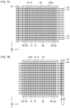
- FIG. 1 is a plan view showing a structure of a solar cell module according to the embodiment
- FIG. 2 is a cross-sectional view showing a structure of the solar cell module of FIG. 1 ;
- FIG. 3 is a perspective view showing a structure of a wire film used in the solar cell module of FIG. 2 ;
- FIGS. 4 A and 4 B are cross-sectional views showing a structure of the first film and the second film exhibited before they are attached to the solar cell of FIG. 2 ;
- FIG. 5 is a partial cross-sectional view showing a structure of the solar cell module of FIG. 2 ;
- FIGS. 6 A and 6 B are plan views showing a structure of the solar cell of FIG. 1 ;
- FIGS. 7 A and 7 B are partial plan views showing a structure of the solar cell module of FIG. 1 ;
- FIGS. 8 A, 8 B, 8 C, and 8 D show a structure of the second type solder layer in the solar cell module of FIG. 1 .
- An embodiment of the present disclosure relates to a solar cell module in which a plurality of solar cells are arranged in a matrix.
- An encapsulant is provided between the first protection member and the second protection member in the solar cell module.
- the encapsulant encapsulates a plurality of solar cell.
- two adjacent solar cells are connected by a wire film.
- a wire film is configured as two films connected by a plurality of wires, and the respective films are adhesively attached to adjacent solar cells, thereby connecting the finger electrodes of the respective solar cells by the plurality of wires. Since the wire plays the role of a wiring member, a string is formed by a plurality of solar cells arranged in a direction of extension of the wire. A wire film like this is used to make it easy to manufacture a solar cell module.
- first film is attached to the light receiving surface of one solar cell
- second film is attached to the back surface of the adjacent solar cell.
- each of the light receiving surface and the back surface of a solar cell is formed by a transparent electrode.
- a plurality of finger electrodes each formed by hard-soldered silver paste and extending in the first direction are arranged in the second direction.
- a plurality of such solar cells are arranged in the second direction and connected by a plurality of wires extending in the second direction, thereby forming a string extending in the second direction.
- a plurality of strings are arranged in the first direction.
- the solar cells provided at the respective ends of two adjacent strings are connected by a bridge wiring member extending in the first direction. As a result, a plurality of strings are connected.
- a solder having a low melting point is provided on the surface of a wire. As the solder is melted, the wire connects a plurality of solar cells or connects the solar cell and the bridge wiring member.
- the wettability of the finger electrode, in which hard-soldered silver paste is used, with a solder of a low melting point is higher than the wettability of the transparent electrode. Therefore, the solder of a low melting point on the transparent electrode is attracted to the finger electrode having a higher wettability as the solder of a low melting point is melted.
- a solder of a high melting point is provided on the surface of the bridge wiring member, and the interval between the bridge wiring member and the solar cell in the second direction is configured to be longer than the interval between finger electrodes adjacent on the solar cell in the second direction.
- the wettability of the bridge wiring member, in which the solder of a high melting point is used, with the solder of a low melting point is higher than the wettability of the finger electrode in which hard-soldered silver paste is used. For this reason, the solder of a low melting point is more attracted to the bridge wiring member than the finger electrode, as the solder of a low melting point is melted.
- the width of the solder of a low melting point in the first direction will be largest in the bridge wiring member, followed by the finger electrode and the transparent electrode in the stated order. This improves the bond strength of the wire in the bridge wiring member and in the finger electrode.
- parallel and perpendicular in the following description not only encompass completely parallel or perpendicular but also encompass off-parallel and off-perpendicular within the margin of error.
- substantially means identical within certain limits.
- FIG. 1 is a plan view showing a structure of a solar cell module 100 .
- an orthogonal coordinate system including an x axis, y axis, and a z axis is defined.
- the x axis and y axis are orthogonal to each other in the plane of the solar cell module 100 .
- the z axis is perpendicular to the x axis and y axis and extends in the direction of thickness of the solar cell module 100 .
- the positive directions of the x axis, y axis, and z axis are defined in the directions of arrows in FIG. 1 , and the negative directions are defined in the directions opposite to those of the arrows.
- FIG. 1 can be said to be a plan view of the solar cell module 100 as viewed from the light receiving surface side.
- the solar cell module 100 includes an 11th solar cell 10 aa , . . . , a 46th solar cell 10 df , which are generically referred to as solar cells 10 , wires 14 , bridge wiring members 16 , terminal wiring members 18 , a first frame 20 a , a second frame 20 b , a third frame 20 c , and a fourth frame 20 d , which are generically referred to as frames 20 .
- the first frame 20 a extends in the x axis direction
- the second frame 20 b extends in the negative direction along the y axis from the positive direction end of the first frame 20 a along the x axis
- the third frame 20 c extends in the negative direction along the x axis from the negative direction end of the second frame 20 b along the y axis
- the fourth frame 20 d connects the negative direction end of the third frame 20 c along the x axis and the negative direction end of the first frame 20 a along the x axis.
- the frames 20 bound the outer circumference of the solar cell module 100 and are made of a metal such as aluminum.
- the first frame 20 a and the third frame 20 c are longer than the second frame 20 b and the fourth frame 20 d , respectively, so that the solar cell module 100 has a rectangular shape longer in the x axis direction than in the y axis direction.
- the shape of the solar cell module 100 is not limited to the illustrated shape.
- Each of the plurality of solar cells 10 absorbs incident light and generates photovoltaic power.
- the solar cell 10 generates an electromotive force from the light absorbed on the light receiving surface and also generates photovoltaic power from the light absorbed on the back surface.
- the solar cell 10 is formed by, for example, a semiconductor material such as crystalline silicon, gallium arsenide (GaAs), or indium phosphorus (InP).
- the structure of the solar cell 10 is not limited to any particular type. It is assumed here that crystalline silicon and amorphous silicon are stacked by way of example.
- the solar cell 10 is formed in a rectangular shape on the x-y plane but may have other shapes. For example, the solar cell 10 may have an octagonal shape.
- a plurality of finger electrodes (not shown in FIG. 1 ) extending in the y axis direction in a mutually parallel manner are disposed on the light receiving surface and the back surface of each solar cell 10 .
- the finger electrode is a collecting
- the plurality of solar cells 10 are arranged in a matrix on the x-y plane.
- six solar cells 10 are arranged in the x axis direction.
- the six solar cells 10 arranged and disposed in the x axis direction are connected in series by the wires 14 so as to form one string 12 .
- a first string 12 a is formed by connecting the 11th solar cell 10 aa , the 12th solar cell 10 ab , . . . , and the 16th solar cell 10 af .
- the second string 12 b through the fourth string 12 d are similarly formed.
- the four strings 12 are arranged in parallel in the y axis direction.
- the number of solar cells 10 arranged in the x axis direction is larger than the number of solar cells 10 arranged in the y axis direction.
- the number of solar cells 10 included in the string 12 is not limited to “6”, and the number of strings 12 is not limited to “4”.
- the wires 14 connect the finger electrodes on the light receiving surface side of one of the solar cells 10 adjacent to each other in the x axis direction to the finger electrodes on the back surface side of the other.
- the five wires 14 for connecting the 11th solar cell 10 aa and the 12th solar cell 10 ab adjacent to each other electrically connect the finger electrodes on the back surface side of the 11th solar cell 10 aa and the finger electrodes on the light receiving surface side of the 12th solar cell 10 ab .
- the number of wires 14 is not limited to “5”. Connection between the wires 14 and the solar cell 10 will be described below.
- the bridge wiring member 16 extends in the y axis direction and electrically connect the two adjacent strings 12 .
- the 16th solar cell 10 af located at the positive direction end of the first string 12 a along the x axis and the 26th solar cell 10 bf located at the positive direction end of the second string 12 b along the x axis are electrically connected by the bridge wiring member 16 .
- the second string 12 b and the third string 12 c are electrically connected by the bridge wiring member 16 at the negative direction end along the x axis
- the third string 12 c and the fourth string 12 d are electrically connected by the bridge wiring member 16 at the positive direction end along the x axis.
- the plurality of strings 12 are connected in series by the bridge wiring member 16 .
- the bridge wiring member 16 is not connected to the 11th solar cell 10 aa at the negative direction end of the first string 12 a along the x axis. Instead the terminal wiring member 18 is connected. The terminal wiring member 18 is also connected to the 41st solar cell 10 da at the negative direction end of the fourth string 12 d along the x axis. A lead wiring member (not shown) is connected to the terminal wiring member 18 . The lead wiring member is a wiring member for retrieving the electric power generated in the plurality of solar cells 10 outside the solar cell module 100 . Given that the bridge wiring member 16 and the terminal wiring member 18 are referred to as “first type wiring member”, the wire 14 is referred to as “second type wiring member”.
- FIG. 2 is a cross sectional view showing a structure of the solar cell module 100 along the x axis and is an A-A cross sectional view of FIG. 1 .
- the solar cell module 100 includes a 12th solar cell 10 ab , a 13th solar cell 10 ac , the wires 14 , a first protection member 30 , a first encapsulant 32 , a second encapsulant 34 , a second protection member 36 , a first film 40 , a second film 42 , a first adhesive agent 44 , and a second adhesive agent 46 .
- the top of FIG. 2 corresponds to the light receiving surface side, and the bottom corresponds to the back surface side.
- the first protection member 30 is disposed on the light receiving surface side of the solar cell module 100 and protects the surface of the solar cell module 100 . Further, the solar cell module 100 is shaped in a rectangle bounded by the frames 20 on the x-y plane. The first protection member 30 is formed by using a translucent and water shielding glass, translucent plastic, etc. The first protection member 30 increases the mechanical strength of the solar cell module 100 .
- the first encapsulant 32 is stacked on the back surface side of the first protection member 30 .
- the first encapsulant 32 is disposed between the first protection member 30 and the solar cell 10 and adhesively bonds the first protection member 30 and the solar cell 10 .
- a thermoplastic resin film of polyolefin, ethylene-vinyl acetate copolymer (EVA), polyvinyl butyral (PVB), polyimide, or the like may be used as the first encapsulant 32 .
- a thermosetting resin may alternatively be used.
- the first encapsulant 32 is formed by a translucent sheet member having a surface of substantially the same dimension as the x-y plane in the first protection member 30 .
- the 12th solar cell 10 ab and the 13th solar cell 10 ac are stacked on the back surface side of the first protection member 30 .
- the solar cells 10 are provided such that the light receiving surface 22 faces the positive direction side along the z axis and the back surface 24 faces the negative direction side along the z axis. Given that the light receiving surface 22 is referred to as the “first surface”, the back surface 24 is referred to as the “second surface”.
- the wires 14 , the first adhesive agent 44 , and the first film 40 are provided on the light receiving surface 22 of the solar cell 10 , and the wires 14 , the second adhesive agent 46 , and the second film 42 are provided on the back surface 24 of the solar cell 10 .
- FIG. 3 will be used to describe the arrangement of the wires 14 , the first film 40 , and the second film 42 in the solar cell 10 .
- FIG. 3 is a perspective view showing a structure of a wire film 90 used in the solar cell module 100 .
- the wire film 90 includes the wires 14 , the first film 40 , the second film 42 , the first adhesive agent 44 , and the second adhesive agent 46 .
- the first film 40 is provided on the side of the light receiving surface 22 of one of the two adjacent solar cells 10 (for example, the 13th solar cell 10 ac ).
- the first adhesive agent 44 is provided on the surface of the first film 40 toward the 13th solar cell 10 ac , and a plurality of wires 14 are provided on the first adhesive agent 44 .
- the first adhesive agent 44 can adhesively bond the first film 40 to the light receiving surface 22 of the 13th solar cell 10 ac.
- the second film 42 is provided on the side of the back surface 24 of the other of the two adjacent solar cells 10 (for example, the 12th solar cell 10 ab ).
- the second adhesive agent 46 is provided on the surface of the second film 42 toward the 12th solar cell 10 ab , and a plurality of wires 14 are provided on the second adhesive agent 46 .
- the second adhesive agent 46 can adhesively bond the second film 42 to the back surface 24 of the 12th solar cell 10 ab.
- the wire film 90 configured as described above and the solar cell module 100 are manufactured separately.
- the first adhesive agent 44 is adhesively bonded to the light receiving surface 22 of the 13th solar cell 10 ac
- the second adhesive agent 46 is adhesively bonded to the back surface 24 of the 12th solar cell 10 ab .
- the wires 14 electrically connect the finger electrodes (not shown) on the light receiving surface 22 of the 13th solar cell 10 ac to the finger electrodes (not shown) on the back surface 24 of the 12th solar cell 10 ab.
- FIGS. 4 A- 4 B are cross-sectional views showing a structure of the first film 40 and the second film 42 exhibited before they are attached to the solar cell 10 .
- FIG. 4 A is a cross-sectional view exhibited when the neighborhood of the 12th solar cell 10 ab of FIG. 2 is severed along the y axis and is a cross-sectional view exhibited before the first film 40 and the second film 42 are attached to the 12th solar cell 10 ab .
- the first film 40 and the second film 42 shown in FIG. 4 A are included in mutually different wire films 90 .
- the first film 40 is formed by a transparent resin film of, for example, polyethylene terephthalate (PET).
- PET polyethylene terephthalate
- the first film 40 has rectangular shape of a size equal to or smaller than the size of the solar cell 10 on the x-y plane.
- polyolefin is used for the first adhesive agent 44 provided on the back surface side of the first film 40 , but EVA may be used.
- the first adhesive agent 44 has a shape similar to that of the first film 40 on the x-y plane.
- a plurality of wires 14 are provided on the back surface side of the first adhesive agent 44 .
- FIG. 4 B is a cross-sectional view of the wire 14 in the same direction as that of FIG. 4 A .
- the wire 14 extends in a cylindrical shape and has a circular cross section.
- the wire 14 has a diameter of 100-500 ⁇ m, and, preferably, 300 ⁇ m, and so is thinner in width of 1-2 mm of a tab line commonly used in a solar cell module.
- the outer circumference of the wire 14 is coated with a second type solder layer 50 having a thickness of 5 ⁇ m to 30 ⁇ m.
- the second type solder layer 50 is formed by a solder having a low melting point.
- the solder has a tin-silver-bismuth composition.
- the melting point of the second type solder layer 50 would be about 140° C.
- FIG. 4 A The figure shows five wires 14 by way of example, but, generally, the number of wires 14 is 10-20, which is larger than the number of tab lines commonly used in a solar cell module.
- the second film 42 is configured in a manner similar to that of the first film 40 .
- polyolefin or EVA is used for the second adhesive agent 46 provided on the light receiving side of the second film 42 .
- the second adhesive agent 46 has a shape similar to that of the second film 42 on the x-y plane.
- a plurality of wires 14 are provided on the light receiving surface side of the second adhesive agent 46 .
- the structure of the wire 14 is as shown in FIG. 4 B . Reference is mad back to FIG. 2 .
- the second encapsulant 34 is stacked on the back surface side of the first encapsulant 32 .
- the second encapsulant 34 encapsulates the plurality of solar cells 10 , the wires 14 , the bridge wiring members 16 , the terminal wiring members 18 , the first films 40 , the second films 42 , etc., sandwiching the cells, the wires, the members, and the films between the first encapsulant 32 and the second encapsulant 34 .
- the same member as used for the first encapsulant 32 may be used for the second encapsulant 34 .
- the second encapsulant 34 is integrated with the first encapsulant 32 by heating the encapsulants in a laminate cure process.
- the second protection member 36 is stacked on the back surface side of the second encapsulant 34 so as to face the first protection member 30 .
- the second protection member 36 protects the back surface side of the solar cell module 100 as a back sheet.
- a resin film of, for example, PET, polytetrafluoroethylene (PTFE), etc., a stack film having a structure in which an Al foil is sandwiched by resin films of, for example, polyolefin, or the like is used as the second protection member 36 .
- FIG. 5 is a partial cross-sectional view showing a structure of the solar cell module 100 viewed in the same direction as FIG. 4 A .
- the first protection member 30 is provided on the side of the light receiving surface 22 of the 12th solar cell 10 ab
- the second protection member 36 is provided on the side of the back surface 24 of the 12th solar cell 10 ab .
- the first encapsulant 32 and the second encapsulant 34 are integrated in a laminate cure process.
- the integrated encapsulant is provided between the first protection member 30 and the second protection member 36 to encapsulate a plurality of solar cells 10 including the 12th solar cell 10 ab , the bridge wiring members 16 (not shown) or the terminal wiring members 18 (not shown).
- the first film 40 is attached to the light receiving surface 22 of the 12th solar cell 10 ab by being bonded by the first adhesive agent 44 of FIG. 4 A .
- the plurality of wires 14 are sandwiched between the first film 40 and the light receiving surface 22 , and the plurality of wires 14 are connected to the plurality of finger electrodes (not shown) on the light receiving surface 22 of the 12th solar cell 10 ab .
- the second film 42 is attached to the back surface 24 of the 12th solar cell 10 ab by being bonded by the second adhesive agent 46 of FIG. 4 A .
- the plurality of wires 14 are sandwiched between the second film 42 and the back surface 24 , and the plurality of wires 14 are connected to the plurality of finger electrodes (not shown) on the back surface 24 of the 12th solar cell 10 ab .
- the plurality of wires 14 and the plurality of finger electrodes on the light receiving surface 22 of the 12th solar cell 10 ab may not be connected by the melting of the second type solder layer 50 , and the second type solder layer 50 and the finger electrodes may be directly in contact.
- FIGS. 6 A- 6 B are plan views showing a structure of the solar cell 10 .
- FIG. 6 A is a plan view showing the 12th solar cell 10 ab of FIG. 5 A as viewed from the side of the light receiving surface 22 .
- a plurality of finger electrodes 60 extending in the y axis direction are arranged in the x axis direction on the light receiving surface 22 .
- the plurality of wires 14 extend on the light receiving surface 22 from the negative direction side along the x axis so as to intersect the plurality of finger electrodes 60 .
- the plurality of wires 14 are sandwiched between the first film 40 and the light receiving surface 22 .
- the first film 40 is configured to be smaller than the light receiving surface 22 .
- FIG. 6 B is a plan view of the 12th solar cell 10 ab of FIG. 5 A viewed from the side of the back surface 24 .
- a plurality of finger electrodes 60 extending in the y axis direction are arranged in the x axis direction on the back surface 24 .
- the number of finger electrodes 60 on the back surface 24 may be larger than the number of finger electrodes 60 on the light receiving surface 22 .
- the interval between adjacent finger electrodes 60 on the back surface 24 is configured to be smaller than the interval between adjacent finger electrodes 60 on the light receiving surface 22 .
- the plurality of wires 14 extend on the light receiving surface 22 from the positive direction side along the x axis so as to intersect the plurality of finger electrodes 60 .
- the plurality of wires 14 are sandwiched between the second film 42 and the back surface 24 .
- the second film 42 is configured to be smaller than the back surface 24 .
- FIGS. 7 A- 7 B are partial plan views showing a structure of the solar cell module 100 .
- FIG. 7 A shows the neighborhood of the 11-th solar cell 10 aa and the terminal wiring member 18 of FIG. 1 .
- a plurality of finger electrodes 60 each extending in the y axis direction are arranged in the x axis direction on the light receiving surface 22 of the 11-th solar cell 10 aa .
- a plurality of wires 14 each extending in the x axis direction are arranged in the y axis direction and are connected to the plurality of finger electrodes 60 , respectively.
- the number of wires 14 is configured to be larger than that described above.
- the plurality of wires 14 and the first film 40 extend from the light receiving surface 22 of the 11-th solar cell 10 aa in the negative direction along the x axis as far as a position overlapping the surface of the terminal wiring member 18 on the light receiving surface side.
- the plurality of wires 14 are connected there to the surface of the terminal wiring member 18 on the light receiving surface side, being sandwiched by the first film 40 and the terminal wiring member 18 .
- the connection of the 31-st solar cell 10 ca and the bridge wiring member 16 in FIG. 1 is of the same structure as that of FIG. 7 A .
- the connection of the 26-th solar cell 10 bf and the bridge wiring member 16 and the connection of the 46-th solar cell 10 df and the bridge wiring member 16 in FIG. 1 are a horizontally flipped image of the structure of FIG. 7 A .
- FIG. 7 B shows the neighborhood of the 16-th solar cell 10 af and the bridge wiring member 16 of FIG. 1 .
- the plurality of finger electrodes 60 , the plurality of wires 14 , and the first film 40 are arranged in a manner similar to that of FIG. 7 A .
- the plurality of first films 40 from the back surface 24 of the 16-th solar cell 10 af extend in the positive direction along the x axis as far as a position overlapping the surface of the bridge wiring member 16 on the light receiving surface side.
- the plurality of wires 14 are connected there to the surface of the bridge wiring member 16 on the light receiving surface side, being sandwiched by the film 48 and the bridge wiring member 16 .
- the film 48 has a structure similar to that of the first film 40 and has a size commensurate with the bridge wiring member 16 .
- the connection of the 36-th solar cell 10 cf and the bridge wiring member 16 in FIG. 1 is of the same structure as that of FIG. 7 B .
- the connection of the 21-th solar cell 10 ba and the bridge wiring member 16 and the connection of the 41-st solar cell 10 da and the terminal wiring member 18 in FIG. 1 are a horizontally flipped image of the structure of FIG. 7 B .
- FIGS. 8 A- 8 D show a structure of the second type solder layer 50 in the solar cell module 100 .
- FIG. 8 A shows the neighborhood of the 11-st solar cell 10 aa and the terminal wiring member 18 like that of FIG. 7 a but is an enlarged view of a portion of the 11-st solar cell 10 aa and the terminal wiring member 18 .
- the first film 40 is omitted from the illustration.
- the light receiving surface 22 of the solar cell 10 is formed by a transparent electrode, and the plurality of finger electrodes 60 provided on the light receiving surface 22 are formed by hard-soldered silver paste.
- the hard-soldered silver paste encompasses a resin hardened at 200-300° C.
- the first type solder layer 52 is provided on the surface of the terminal wiring member 18 on the light receiving surface side.
- the first type solder layer 52 is formed by a solder having a higher melting point than the second type solder layer 50 .
- the first type solder layer 52 has a tin-silver-copper composition. In that case, the melting point of the first type solder layer 52 is about 220° C.
- the minimal interval between the terminal wiring member 18 and the 11-st solar cell 10 aa in the x axis direction is denoted by a first interval D 1 .
- the interval between two adjacent finger electrodes 60 in the x axis direction is denoted by a second interval D 2 .
- the first interval D 1 is 3-5 mm by way of one example
- the second interval D 2 is 2 mm by way of one example. In other words, the first interval D 1 is configured to be larger than the second interval D 2 .
- the hard-soldered silver paste used in the plurality of finger electrodes 60 contains an additive such as a conductive filler, a binder resin, and a solvent.
- Metal particles of silver (Ag), copper (Cu), nickel (Ni), etc., or carbon, or a mixture thereof are/is used for the conductive filler. Of these, Ag particles are suitable.
- the binder resin be a thermosetting resin.
- the binder resin not hardened yet is in a solid state that is soluble in a solvent or in a liquid or paste state (semisolid state) at room temperature.
- Further conductive paste A, B contains, as necessary, a hardening agent adapted to the binder resin.
- the additive is exemplified by a rheology conditioner, a plasticizer, a dispersant, a defoamant, etc.
- FIG. 8 B is a cross-sectional view of a first portion P 1 of FIG. 8 A
- FIG. 8 C is a cross-sectional view of a second portion P 2 of FIG. 8 A
- FIG. 8 D is a cross-sectional view of a third portion P 3 of FIG. 8 A
- the left side corresponds to the light receiving surface side
- the right side corresponds to the back surface side.
- the first portion P 1 in FIG. 8 B is a portion where the wire 14 is connected to the terminal wiring member 18 .
- the first type solder layer 52 is provided on the light receiving surface side of the terminal wiring member 18
- the wire 14 is connected to the first type solder layer 52 by the second type solder layer 50 .
- the first film 40 is provided to cover the first type solder layer 52 , the second type solder layer 50 , and the wire 14 .
- the second portion P 2 in FIG. 8 C is a portion where the wire 14 is connected to the finger electrode 60 .
- the finger electrode 60 is provided on the light receiving surface 22 of the 11-st solar cell 10 aa , and the wire 14 is connected to the finger electrode 60 by the second type solder layer 50 .
- the first film 40 is provided to cover the finger electrode 60 , the second type solder layer 50 , and the wire 14 .
- the third portion P 3 in FIG. 8 D is a portion where the wire 14 is brought into contact with the light receiving surface 22 , i.e., the transparent electrode.
- the wire 14 is connected to the light receiving surface 22 of the 11-st solar cell 10 aa by the second type solder layer 50 .
- the first film 40 is provided to cover the light receiving surface 22 , the second type solder layer 50 , and the wire 14 .
- the wettability of the finger electrode 60 in which hard-soldered silver paste is used, with the second type solder layer 50 is higher than the wettability of the transparent electrode on the light receiving surface 22 .
- the second type solder layer 50 on the transparent electrode is attracted to the finger electrode 60 having a higher wettability as the second type solder layer 50 is melted.
- a second width W 2 of the second type solder layer 50 in the second portion P 2 shown in FIG. 8 C in the y axis direction is larger than a third width W 3 of the second type solder layer 50 in the third portion P 3 shown in FIG. 8 D in the y axis direction.
- the wettability of the terminal wiring member 18 , in which the first type solder layer 52 is used, with the second type solder layer 50 is higher than the wettability of the finger electrode 60 in which hard-soldered silver paste is used. Therefore, the second type solder layer 50 is more attracted to the terminal wiring member 18 than the finger electrode 60 as the second type solder layer 50 is melted. Further, as shown in FIG. 8 A , the first interval D 1 is configured to be longer than the second interval D 2 . For this reason, the amount of the second type solder layer 50 attracted by the terminal wiring member 18 is larger than the mount of the second type solder layer 50 attracted by the finger electrode 60 . As a result, a first width W 1 of the second type solder layer 50 in the first portion P 1 shown in FIG. 8 B in the y axis direction is larger than the second width W 2 shown in FIG. 8 C .
- the width of the second type solder layer 50 in the y axis direction is largest in the terminal wiring member 18 .
- the width of the second type solder layer 50 is next largest in the finger electrode 60 . Further, the width of the second type solder layer 50 is smallest in the transparent electrode. This improves the bond strength of the wire 14 in the terminal wiring member 18 and in the finger electrode 60 .
- the above description applies to the bridge wiring member 16 as well as to the terminal wiring member 18 .
- the wire film 90 shown in FIG. 3 is prepared to connect two adjacent solar cells 10 .
- the string 12 is produced by layering the first film 40 of the wire film 90 on one of the two adjacent solar cells 10 and layering the second film 42 of the wire film 90 on the other of the two adjacent solar cells 10 .
- Either the bridge wiring member 16 or the terminal wiring member 18 is attached to the end of the string 12 via the wire 14 .
- a stack is produced by layering the first protection member 30 , the first encapsulant 32 , the string 12 , the bridge wiring member 16 and the terminal wiring member 18 , the second encapsulant 34 , and the second protection member 36 in the stated order in the positive-to-negative direction along the z axis.
- a laminate cure process performed for the stack.
- air is drawn from the stack, and the stack is heated and pressurized so as to be integrated.
- the temperature is set to about 50-140°, as mentioned before. The temperature is higher than the melting point of the second type solder layer 50 and lower than the melting point of the first type solder layer 52 .
- a terminal box is attached to the second protection member 36 using an adhesive.
- the finger electrode 60 is formed by hard-soldered silver paste, and the melting point of the first type solder layer 52 is configured to be higher than the melting point of the second type solder layer 50 . Therefore, the second type solder layer 50 is more attracted to the bridge wiring member 16 or the terminal wiring member 18 than the finger electrode 60 . Further, since the second type solder layer 50 is more attracted to the bridge wiring member 16 or the terminal wiring member 18 than the finger electrode 60 , the first width W 1 of the second type solder layer 50 in the first portion P 1 is configured to be larger than the second width W 2 of the second type solder layer 50 in the second portion P 2 .
- the first interval D 1 between the solar cell 10 and the bridge wiring member 16 or the terminal wiring member 18 is configured to be wider than the second interval D 2 between two adjacent finger electrodes 60 , the amount of the second type solder layer 50 attracted to the bridge wiring member 16 or the terminal wiring member 18 is increased. Further, since the amount of the second type solder layer 50 attracted to the bridge wiring member 16 or the terminal wiring member 18 is increased, the first width W 1 of the second type solder layer 50 in the first portion P 1 is configured to be larger than the second width W 2 of the second type solder layer 50 in the second portion P 2 .
- first width W 1 of the second type solder layer 50 in the first portion P 1 is configured to be larger than the second width W 2 of the second type solder layer 50 in the second portion P 2 , the bond strength of the wire 14 in the bridge wiring member 16 or in the terminal wiring member 18 is improved. Since the bond strength of the wire 14 in the bridge wiring member 16 or in the terminal wiring member 18 is improved, the durability is inhibited from being lowered. Since the wire film 90 is used to connect a plurality of solar cells 10 , the manufacturing of the solar cell module 100 is made easy.
- the manufacturing of the solar cell module 100 is made easier.
- the first type solder layer 52 has a tin-silver-copper composition
- the second type solder layer 50 has a tin-silver-bismuth composition
- the melting point of the first type solder layer 52 is configured to be lower than the melting point of the second type solder layer 50 .
- the transparent electrode is provided on the light receiving surface 22 of the solar cell 10 , it is ensured that the second type solder layer 50 is more attracted to the finger electrode 60 than the transparent electrode. Further, since the second type solder layer 50 is more attracted to the finger electrode 60 than the transparent electrode, the second width W 2 is configured to be larger than the third width W 3 of the second type solder layer 50 in the third portion P 3 . Further, since the second width W 2 is configured to be larger than the third width W 3 of the second type solder layer 50 in the third portion P 3 , the bond strength of the wire 14 in the finger electrode 60 is improved. Since the bond strength of the wire 14 in the finger electrode 60 is improved, the durability is inhibited from being lowered.
- a solar cell module 100 includes: a solar cell 10 including a light receiving surface 22 and a back surface 24 that face in opposite directions, a plurality of finger electrodes 60 each extending in a first direction being arranged on the light receiving surface 22 in a second direction intersecting the first direction; a bridge wiring member 16 , a terminal wiring member 18 that extends in the first direction at a position more spaced apart from the solar cell 10 in the second direction than an interval between two adjacent finger electrodes 60 in the second direction; a first protection member 30 provided on a side of the light receiving surface 22 of the solar cell 10 ; a second protection member 36 provided on a side of the back surface 24 of the solar cell 10 ; a first encapsulant 32 , a second encapsulant 34 provided between the first protection member 30 and the second protection member 36 to encapsulate the solar cell 10 and the bridge wiring member 16 , the terminal wiring member 18 ; a first film 40 attached to the light receiving surface 22 of
- Each of the finger electrodes 60 is formed by hard-soldered silver paste, a melting point of a first type solder layer 52 provided on a surface of the bridge wiring member 16 , the terminal wiring member 18 is higher than a melting point of a second type solder layer 50 provided on a surface of the wire, and a first width W 1 , in the first direction, of the second type solder layer 50 in a first portion P 1 where the wire 14 is connected to the bridge wiring member 16 , the terminal wiring member 18 is larger than a second width W 2 , in the first direction, of the second type solder layer 50 in a second portion P 2 where the wire 14 is connected to the finger electrode 60 .
- the first film 40 may extend in the second direction, and the wire 14 may be connected to the bridge wiring member 16 , the terminal wiring member 18 such that the wire 14 is sandwiched by the first film 40 and the bridge wiring member 16 , the terminal wiring member 18 .
- the first type solder layer 52 may have a tin-silver-copper composition.
- the second type solder layer 50 may have a tin-silver-bismuth composition.
- a transparent electrode is provided on the light receiving surface 22 of the solar cell 10 , and the second width W 2 is larger than a third width W 3 , in the first direction, of the second type solder layer 50 in a third portion P 3 where the wire 14 is in contact with the transparent electrode.
Abstract
Description
Claims (22)
Applications Claiming Priority (3)
| Application Number | Priority Date | Filing Date | Title |
|---|---|---|---|
| JP2018-245939 | 2018-12-27 | ||
| JPJP2018-245939 | 2018-12-27 | ||
| JP2018245939A JP2020107758A (en) | 2018-12-27 | 2018-12-27 | Solar cell module |
Publications (2)
| Publication Number | Publication Date |
|---|---|
| US20200212233A1 US20200212233A1 (en) | 2020-07-02 |
| US11652178B2 true US11652178B2 (en) | 2023-05-16 |
Family
ID=68965779
Family Applications (1)
| Application Number | Title | Priority Date | Filing Date |
|---|---|---|---|
| US16/725,927 Active 2040-06-29 US11652178B2 (en) | 2018-12-27 | 2019-12-23 | Solar cell module including solar cells |
Country Status (4)
| Country | Link |
|---|---|
| US (1) | US11652178B2 (en) |
| EP (1) | EP3675180B1 (en) |
| JP (1) | JP2020107758A (en) |
| CN (1) | CN111403509B (en) |
Families Citing this family (1)
| Publication number | Priority date | Publication date | Assignee | Title |
|---|---|---|---|---|
| WO2023279167A1 (en) * | 2021-07-09 | 2023-01-12 | Newsouth Innovations Pty Limited | Solar cell structure |
Citations (16)
| Publication number | Priority date | Publication date | Assignee | Title |
|---|---|---|---|---|
| US20050241692A1 (en) | 2002-08-29 | 2005-11-03 | Rubin Leonid B | Electrode for photovoltaic cells, photovoltaic cell and photovoltaic module |
| US20070175509A1 (en) | 2006-02-01 | 2007-08-02 | Sanyo Electric Co., Ltd. | Solar battery module |
| JP2007235113A (en) | 2006-02-01 | 2007-09-13 | Sanyo Electric Co Ltd | Solar cell module |
| US20100146745A1 (en) * | 2008-12-12 | 2010-06-17 | Sen-Mei Cheng | Fastening assembly and cushion having fastening assembly |
| US20110146745A1 (en) * | 2007-08-09 | 2011-06-23 | Mitsubishi Electric Corporation | Solar battery panel |
| US20110277835A1 (en) * | 2010-07-23 | 2011-11-17 | Cyrium Technologies Incorporated | Solar cell with split gridline pattern |
| US20120305048A1 (en) * | 2011-05-31 | 2012-12-06 | Hitachi Chemical Company, Ltd. | Solar battery cell, solar battery module and method of making solar battery module |
| US20130125974A1 (en) * | 2010-05-14 | 2013-05-23 | Silevo, Inc. | Solar cell with metal grid fabricated by electroplating |
| US20150083187A1 (en) * | 2012-06-29 | 2015-03-26 | Sanyo Electric Co., Ltd. | Solar cell module and solar cell module manufacturing method |
| US20150372177A1 (en) | 2014-06-18 | 2015-12-24 | Lg Electronics Inc. | Solar cell module |
| US20160093752A1 (en) * | 2014-09-30 | 2016-03-31 | Lg Electronics Inc. | Solar cell and solar cell panel including the same |
| US20160172510A1 (en) * | 2014-12-10 | 2016-06-16 | Solarworld Innovations Gmbh | Photovoltaic module |
| US20160308082A1 (en) | 2013-12-27 | 2016-10-20 | Panasonic Intellectual Property Management Co., Ltd. | Solar cell module |
| US20170104114A1 (en) | 2015-10-08 | 2017-04-13 | Lg Electronics Inc. | Solar cell module |
| EP3244454A1 (en) | 2015-01-05 | 2017-11-15 | Jolywood(Suzhou) Sunwatt Co., Ltd | Main-gate-free high-efficiency back contact solar cell and assembly and preparation process thereof |
| WO2018051658A1 (en) | 2016-09-13 | 2018-03-22 | パナソニックIpマネジメント株式会社 | Solar cell module |
Family Cites Families (4)
| Publication number | Priority date | Publication date | Assignee | Title |
|---|---|---|---|---|
| JP2007201291A (en) * | 2006-01-27 | 2007-08-09 | Kyocera Corp | Solar battery module and method of reproducing same |
| DE112012001641T5 (en) * | 2011-04-11 | 2014-02-06 | Mitsubishi Electric Corp. | Solar battery module and manufacturing method for it |
| US9484479B2 (en) * | 2011-11-09 | 2016-11-01 | Mitsubishi Electric Corporation | Solar cell module and manufacturing method thereof |
| JP2018056490A (en) * | 2016-09-30 | 2018-04-05 | パナソニックIpマネジメント株式会社 | Solar cell module and solar cell |
-
2018
- 2018-12-27 JP JP2018245939A patent/JP2020107758A/en active Pending
-
2019
- 2019-12-19 EP EP19217829.1A patent/EP3675180B1/en active Active
- 2019-12-23 US US16/725,927 patent/US11652178B2/en active Active
- 2019-12-26 CN CN201911365186.XA patent/CN111403509B/en active Active
Patent Citations (22)
| Publication number | Priority date | Publication date | Assignee | Title |
|---|---|---|---|---|
| JP2010045402A (en) | 2002-08-29 | 2010-02-25 | Day4 Energy Inc | Electrode for photovoltaic cells, photovoltaic cell, and photovoltaic module |
| US20050241692A1 (en) | 2002-08-29 | 2005-11-03 | Rubin Leonid B | Electrode for photovoltaic cells, photovoltaic cell and photovoltaic module |
| US20070175509A1 (en) | 2006-02-01 | 2007-08-02 | Sanyo Electric Co., Ltd. | Solar battery module |
| JP2007235113A (en) | 2006-02-01 | 2007-09-13 | Sanyo Electric Co Ltd | Solar cell module |
| US20110146745A1 (en) * | 2007-08-09 | 2011-06-23 | Mitsubishi Electric Corporation | Solar battery panel |
| US20100146745A1 (en) * | 2008-12-12 | 2010-06-17 | Sen-Mei Cheng | Fastening assembly and cushion having fastening assembly |
| US20130125974A1 (en) * | 2010-05-14 | 2013-05-23 | Silevo, Inc. | Solar cell with metal grid fabricated by electroplating |
| US20110277835A1 (en) * | 2010-07-23 | 2011-11-17 | Cyrium Technologies Incorporated | Solar cell with split gridline pattern |
| US20120305048A1 (en) * | 2011-05-31 | 2012-12-06 | Hitachi Chemical Company, Ltd. | Solar battery cell, solar battery module and method of making solar battery module |
| US20150083187A1 (en) * | 2012-06-29 | 2015-03-26 | Sanyo Electric Co., Ltd. | Solar cell module and solar cell module manufacturing method |
| US20160308082A1 (en) | 2013-12-27 | 2016-10-20 | Panasonic Intellectual Property Management Co., Ltd. | Solar cell module |
| US20150372177A1 (en) | 2014-06-18 | 2015-12-24 | Lg Electronics Inc. | Solar cell module |
| JP2016005002A (en) | 2014-06-18 | 2016-01-12 | エルジー エレクトロニクス インコーポレイティド | Solar cell module |
| US20160093752A1 (en) * | 2014-09-30 | 2016-03-31 | Lg Electronics Inc. | Solar cell and solar cell panel including the same |
| US20160172510A1 (en) * | 2014-12-10 | 2016-06-16 | Solarworld Innovations Gmbh | Photovoltaic module |
| EP3244454A1 (en) | 2015-01-05 | 2017-11-15 | Jolywood(Suzhou) Sunwatt Co., Ltd | Main-gate-free high-efficiency back contact solar cell and assembly and preparation process thereof |
| US20170365731A1 (en) | 2015-01-05 | 2017-12-21 | Jolywood (Suzhou) Sunwatt Co., Ltd. | Main-gate-free and high-efficiency back-contact solar cell module, main-gate-free and high-efficiency back-contact assembly, and preparation process thereof |
| US20170104114A1 (en) | 2015-10-08 | 2017-04-13 | Lg Electronics Inc. | Solar cell module |
| EP3163630A1 (en) | 2015-10-08 | 2017-05-03 | LG Electronics Inc. | Solar cell module |
| US20190288135A1 (en) | 2015-10-08 | 2019-09-19 | Lg Electronics Inc. | Solar cell module |
| WO2018051658A1 (en) | 2016-09-13 | 2018-03-22 | パナソニックIpマネジメント株式会社 | Solar cell module |
| US20190207045A1 (en) | 2016-09-13 | 2019-07-04 | Panasonic Intellectual Property Management Co., Ltd. | Solar cell module including a plurality of solar cells |
Non-Patent Citations (1)
| Title |
|---|
| Extended European Search Report issued in European Patent Application No. 19217829.1, dated Feb. 28, 2020. |
Also Published As
| Publication number | Publication date |
|---|---|
| JP2020107758A (en) | 2020-07-09 |
| US20200212233A1 (en) | 2020-07-02 |
| EP3675180A1 (en) | 2020-07-01 |
| CN111403509B (en) | 2023-10-10 |
| EP3675180B1 (en) | 2024-02-07 |
| CN111403509A (en) | 2020-07-10 |
Similar Documents
| Publication | Publication Date | Title |
|---|---|---|
| US20190207045A1 (en) | Solar cell module including a plurality of solar cells | |
| EP2600419B1 (en) | Solar cell module | |
| US20200105954A1 (en) | Solar cell module including a plurality of solar cells connected and method of manufacturing a solar cell module | |
| US20100229918A1 (en) | SOLAR CELL MODULE and MANUFACTURING METHOD OF SOLAR CELL MODULE | |
| US11652178B2 (en) | Solar cell module including solar cells | |
| JP2018046112A (en) | Solar cell module | |
| JP2017174986A (en) | Solar battery cell and solar battery module | |
| US20180097135A1 (en) | Solar cell module and solar cell in which wiring member is connected to surface | |
| US11075312B2 (en) | Solar cell module and method for manufacturing solar cell module | |
| JP2014175520A (en) | Solar battery module and manufacturing method for the same | |
| US20200168755A1 (en) | Solar cell module including a plurality of solar cells | |
| US20190305145A1 (en) | Solar cell module and solar cell including collecting electrodes on both surfaces | |
| US20210066523A1 (en) | Solar cell module including solar cell | |
| US11522095B2 (en) | Solar cell module including solar cells, method of manufacturing solar cell module | |
| CN116053346A (en) | Double-sided light-receiving solar cell module | |
| EP3534409A1 (en) | Solar cell module | |
| US20190221680A1 (en) | Solar cell module including terminal box and method of manufacturing solar cell | |
| JP2002141535A (en) | Method of taking out power leads of solar cell module | |
| US20230146682A1 (en) | Conductive interconnection member of imbricate assembly, imbricate assembly, and manufacturing method | |
| US20200194606A1 (en) | Solar cell module | |
| US20170207359A1 (en) | Solar cell module including wiring layer overlappingly disposed on solar cell | |
| WO2020066395A1 (en) | Solar cell module manufacturing method and solar cell module | |
| JP2017183650A (en) | Solar cell, solar cell module, manufacturing method of solar cell | |
| JP2020098902A (en) | Solar cell module | |
| WO2017150372A1 (en) | Solar battery module and method for manufacturing solar battery module |
Legal Events
| Date | Code | Title | Description |
|---|---|---|---|
| FEPP | Fee payment procedure |
Free format text: ENTITY STATUS SET TO UNDISCOUNTED (ORIGINAL EVENT CODE: BIG.); ENTITY STATUS OF PATENT OWNER: LARGE ENTITY |
|
| STPP | Information on status: patent application and granting procedure in general |
Free format text: DOCKETED NEW CASE - READY FOR EXAMINATION |
|
| AS | Assignment |
Owner name: PANASONIC CORPORATION, JAPAN Free format text: ASSIGNMENT OF ASSIGNORS INTEREST;ASSIGNORS:HASHIMOTO, HARUHISA;MAKI, KENICHI;SIGNING DATES FROM 20191111 TO 20191112;REEL/FRAME:052018/0601 |
|
| STPP | Information on status: patent application and granting procedure in general |
Free format text: NON FINAL ACTION MAILED |
|
| STPP | Information on status: patent application and granting procedure in general |
Free format text: RESPONSE TO NON-FINAL OFFICE ACTION ENTERED AND FORWARDED TO EXAMINER |
|
| STPP | Information on status: patent application and granting procedure in general |
Free format text: FINAL REJECTION MAILED |
|
| STPP | Information on status: patent application and granting procedure in general |
Free format text: DOCKETED NEW CASE - READY FOR EXAMINATION |
|
| AS | Assignment |
Owner name: PANASONIC HOLDINGS CORPORATION, JAPAN Free format text: CHANGE OF NAME;ASSIGNOR:PANASONIC CORPORATION;REEL/FRAME:059909/0607 Effective date: 20220401 |
|
| STPP | Information on status: patent application and granting procedure in general |
Free format text: NON FINAL ACTION MAILED |
|
| STPP | Information on status: patent application and granting procedure in general |
Free format text: RESPONSE TO NON-FINAL OFFICE ACTION ENTERED AND FORWARDED TO EXAMINER |
|
| STCF | Information on status: patent grant |
Free format text: PATENTED CASE |